ECE2030 Introduction to Computer Engineering
Lecture 10: Building Blocks for Combinational Logic (1) Timing Diagram, Mux/DeMux
Prof. Hsien-Hsin Sean LeeProf. Hsien-Hsin Sean Lee
School of Electrical and Computer EngineeringSchool of Electrical and Computer Engineering
Georgia TechGeorgia Tech
2
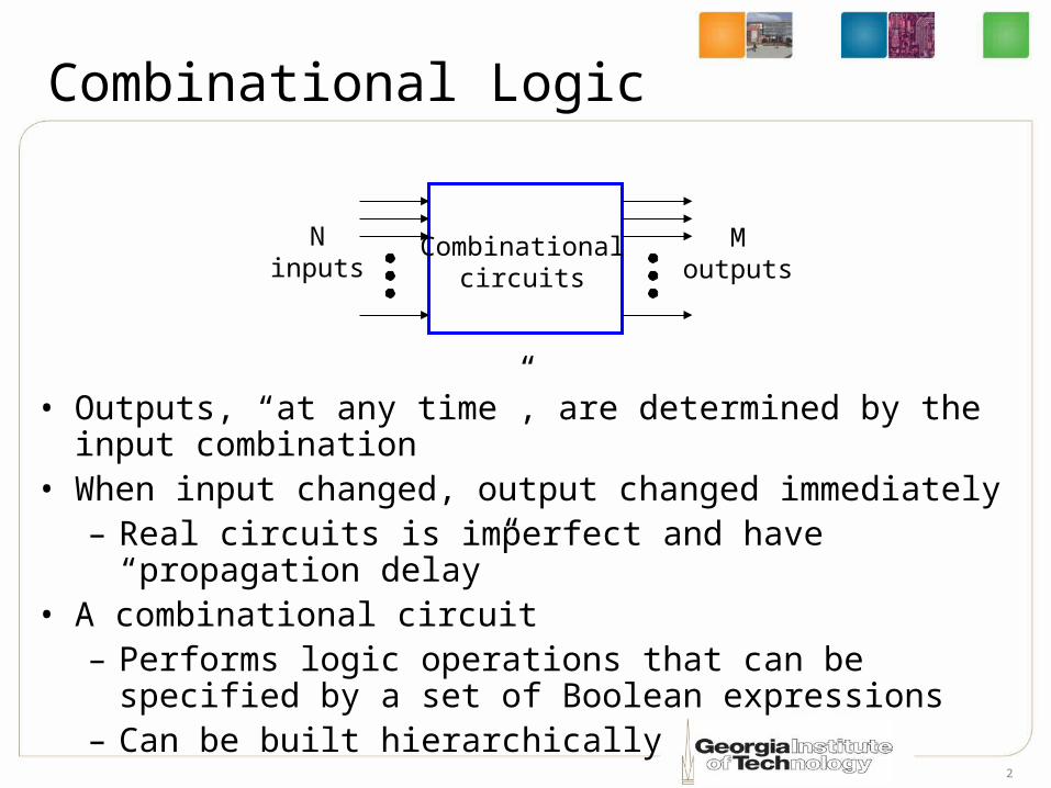
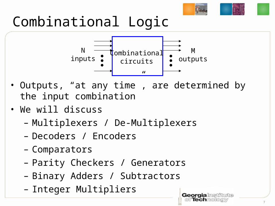
Combinational Logic
• Outputs, “at any time”, are determined by the input combination
• When input changed, output changed immediately– Real circuits is imperfect and have “propagation
delay”• A combinational circuit
– Performs logic operations that can be specified by a set of Boolean expressions
– Can be built hierarchically
Combinationalcircuits
Ninputs
Moutputs
3
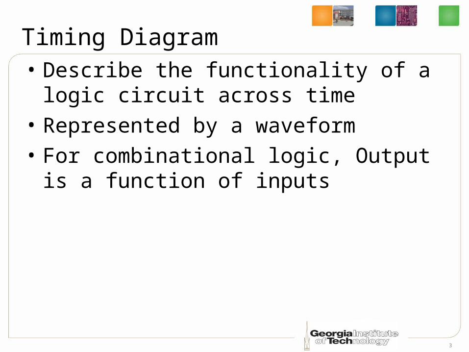
Timing Diagram• Describe the functionality of a logic
circuit across time• Represented by a waveform• For combinational logic, Output is a
function of inputs
4
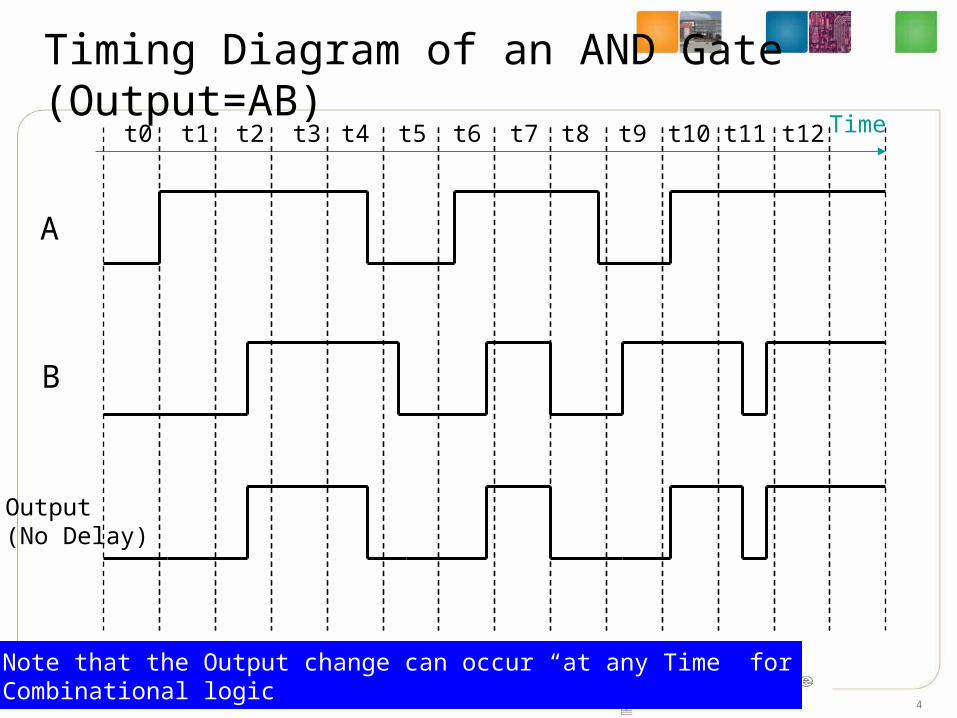
Timing Diagram of an AND Gate (Output=AB)
Time
A
B
Output(No Delay)
t0 t1 t2 t3 t4 t5 t6 t7 t8 t9 t10 t11 t12
Note that the Output change can occur “at any Time” forCombinational logic

5
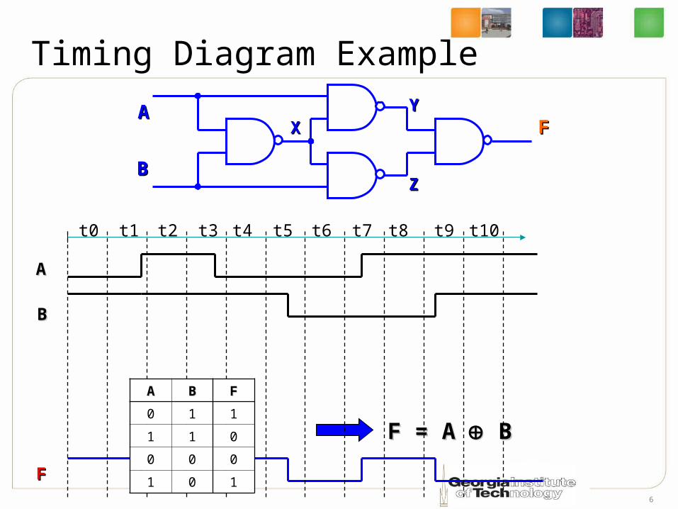
Timing Diagram Example
XXYY
ZZ
FFAA
BB
AA
BB
XX
YY
ZZ
FF
t0 t1 t2 t3 t4 t5 t6 t7 t8 t9 t10
6
Timing Diagram Example
XXYY
ZZ
FFAA
BB
AA
BB
FF
AA BB FF
0 1 1
1 1 0
0 0 0
1 0 1
F = AF = A B B
t0 t1 t2 t3 t4 t5 t6 t7 t8 t9 t10
7
Combinational Logic
• Outputs, “at any time”, are determined by the input combination
• We will discuss– Multiplexers / De-Multiplexers– Decoders / Encoders– Comparators– Parity Checkers / Generators– Binary Adders / Subtractors– Integer Multipliers
Combinationalcircuits
Ninputs
Moutputs
8
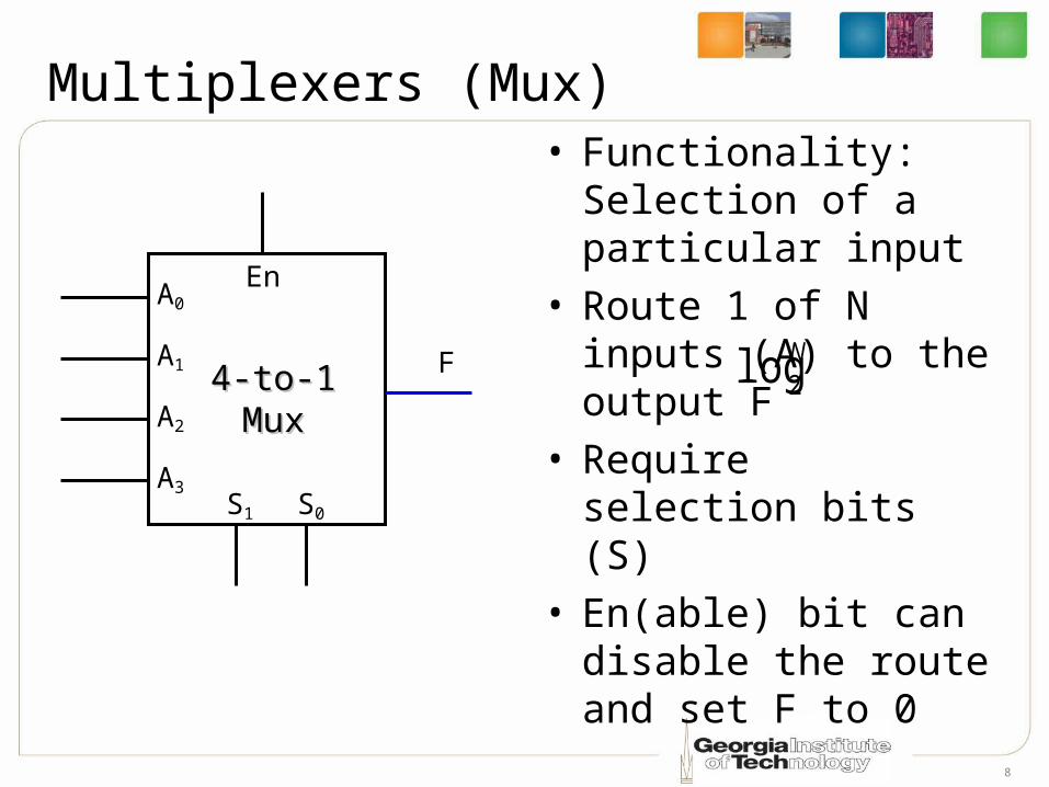
Multiplexers (Mux)• Functionality:
Selection of a particular input
• Route 1 of N inputs (A) to the output F
• Require selection bits (S)
• En(able) bit can disable the route and set F to 0
F
A0
A1
A2
A3S1 S0
En
4-to-14-to-1MuxMux
N2log
9
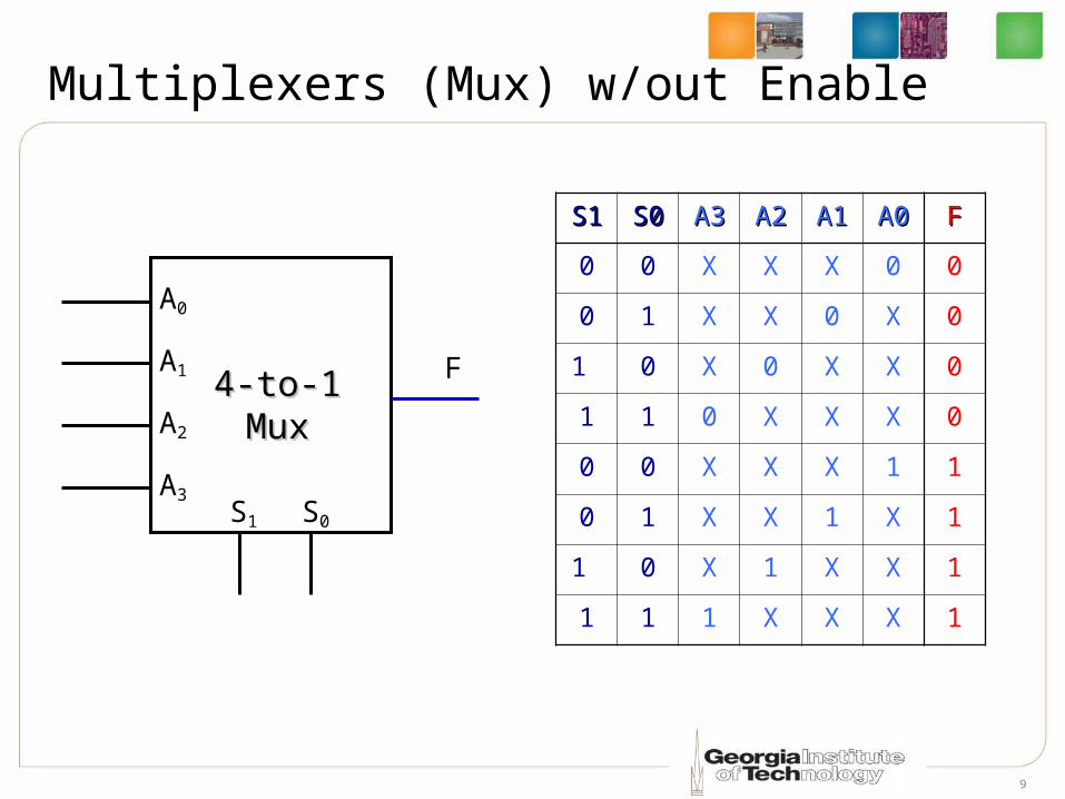
Multiplexers (Mux) w/out Enable
F
A0
A1
A2
A3S1 S0
4-to-14-to-1MuxMux
S1S1 S0S0 A3A3 A2A2 A1A1 A0A0 FF
0 0 X X X 0 0
0 1 X X 0 X 0
1 0 X 0 X X 0
1 1 0 X X X 0
0 0 X X X 1 1
0 1 X X 1 X 1
1 0 X 1 X X 1
1 1 1 X X X 1
10
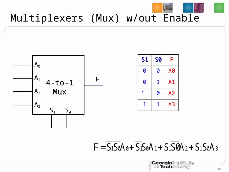
Multiplexers (Mux) w/out Enable
S1S1 S0S0 FF
0 0 A0
0 1 A1
1 0 A2
1 1 A3
F
A0
A1
A2
A3S1 S0
4-to-14-to-1MuxMux
30121101 001 ASSAS0SASSASSF
11
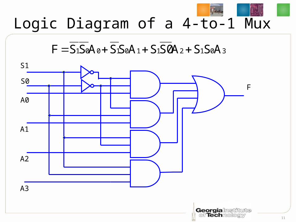
Logic Diagram of a 4-to-1 Mux
30121101 001 ASSAS0SASSASSF S1
S0
A0
A1
A2
A3
F
12
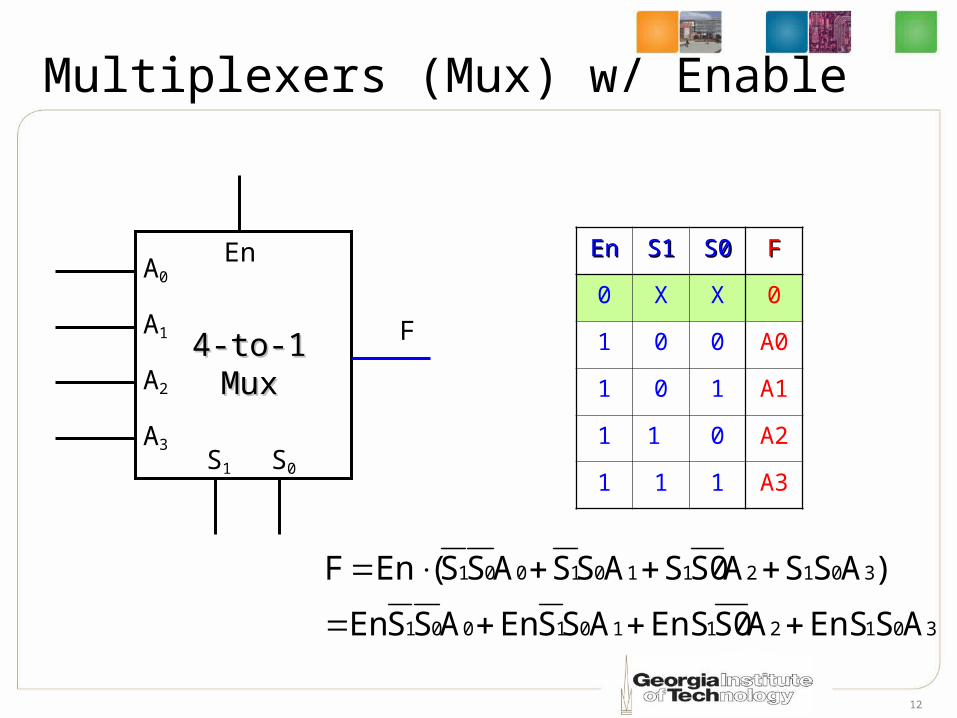
Multiplexers (Mux) w/ Enable
EnEn S1S1 S0S0 FF
0 X X 0
1 0 0 A0
1 0 1 A1
1 1 0 A2
1 1 1 A3
30121101 001
30121101 001
ASEnSAS0EnSASSEnASSEn
)ASSAS0SASSASS(EnF
F
A0
A1
A2
A3S1 S0
En
4-to-14-to-1MuxMux
13
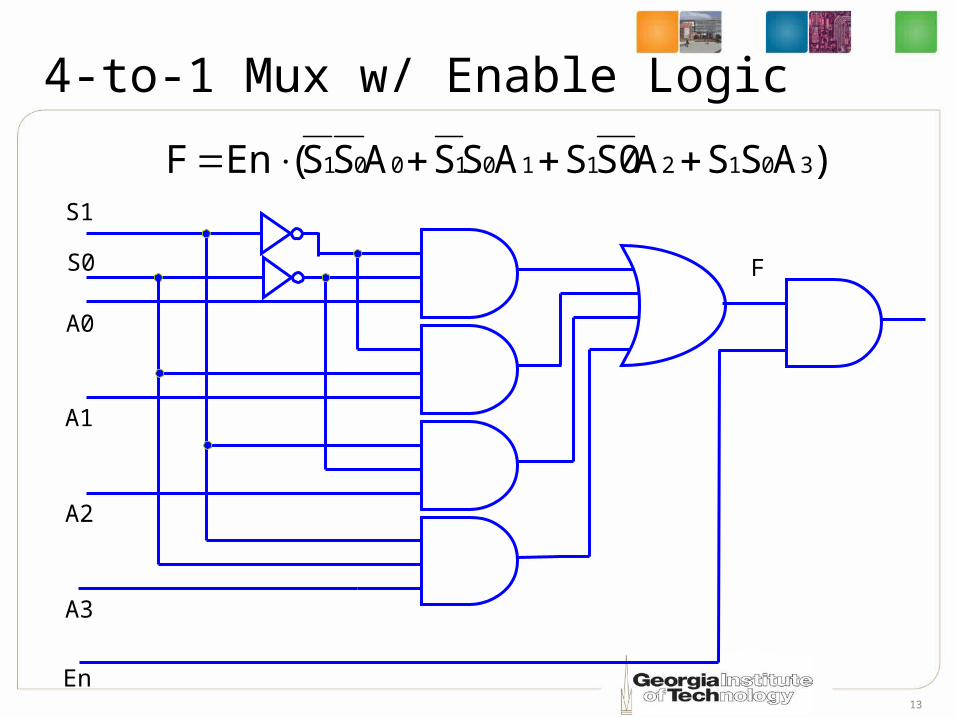
4-to-1 Mux w/ Enable Logic
)ASSAS0SASSASS(EnF 30121101 001 S1
S0
A0
A1
A2
A3
F
En
14
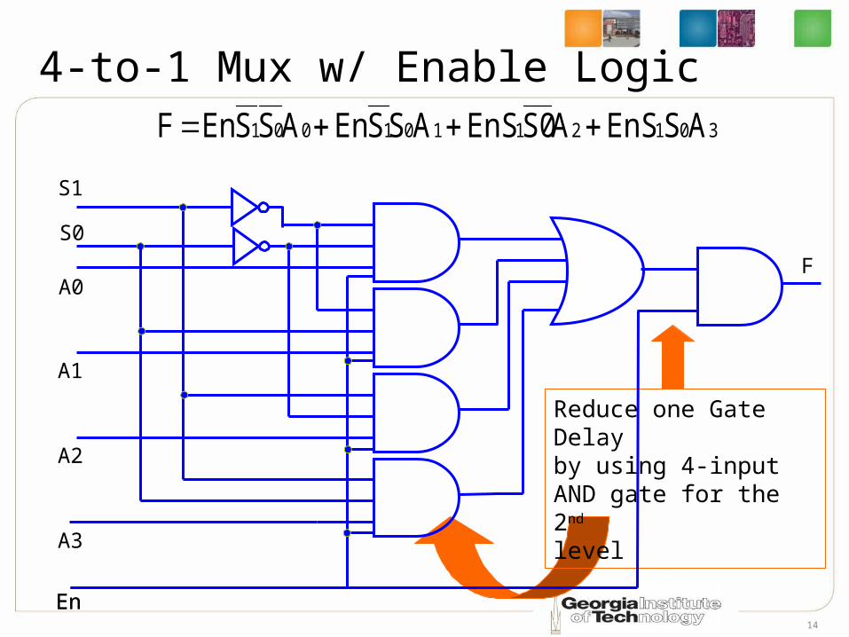
4-to-1 Mux w/ Enable Logic30121101 001 ASEnSAS0EnSASSEnASSEnF
S1
S0
A0
A1
A2
A3
F
En
Reduce one Gate Delayby using 4-input AND gate for the 2nd level
En
15
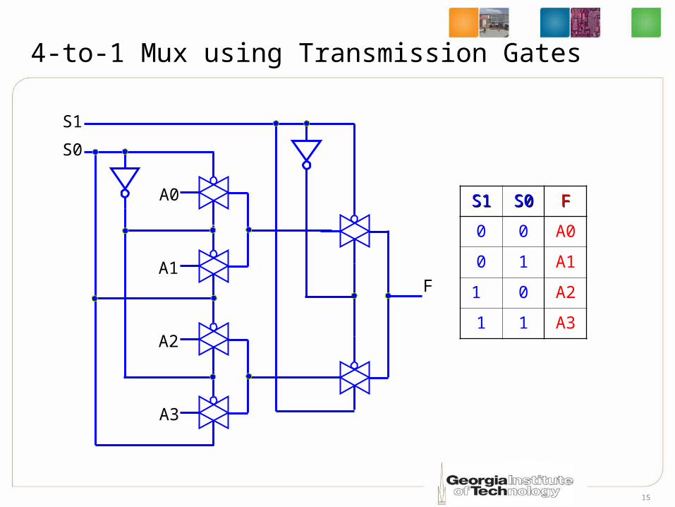
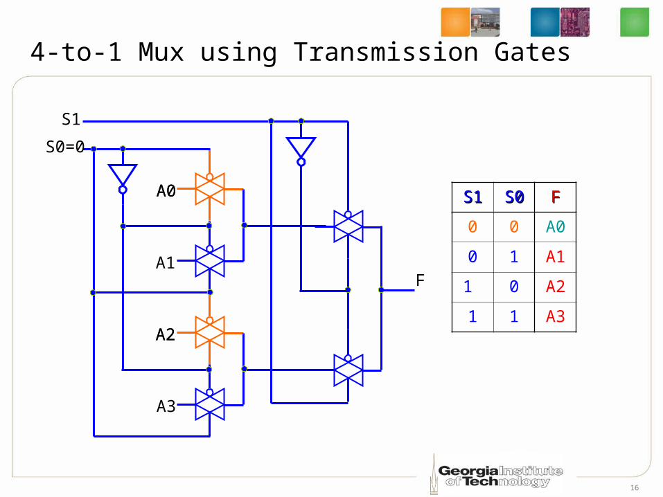
4-to-1 Mux using Transmission Gates
A0
A1
A2
A3
S0
S1
F
S1S1 S0S0 FF
0 0 A0
0 1 A1
1 0 A2
1 1 A3
16
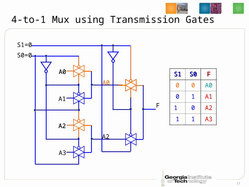
4-to-1 Mux using Transmission Gates
A0
A1
A2
A3
S0=0
S1
F
S1S1 S0S0 FF
0 0 A0
0 1 A1
1 0 A2
1 1 A3
A0
A2
17
4-to-1 Mux using Transmission Gates
A0
A1
A2
A3
F
S1S1 S0S0 FF
0 0 A0
0 1 A1
1 0 A2
1 1 A3
A0
A2
A0
A2
S0=0
S1=0
18
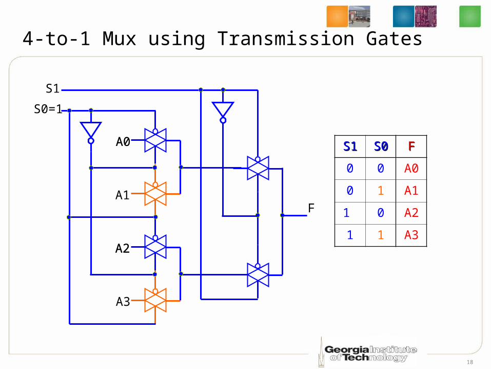
4-to-1 Mux using Transmission Gates
A0
A1
A2
A3
S0=1
S1
F
S1S1 S0S0 FF
0 0 A0
0 1 A1
1 0 A2
1 1 A3
A0
A2
19
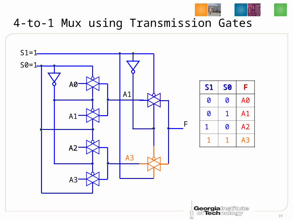
4-to-1 Mux using Transmission Gates
A0
A1
A2
A3
F
S1S1 S0S0 FF
0 0 A0
0 1 A1
1 0 A2
1 1 A3
A0
A2
A1
A3
S0=1
S1=1
20
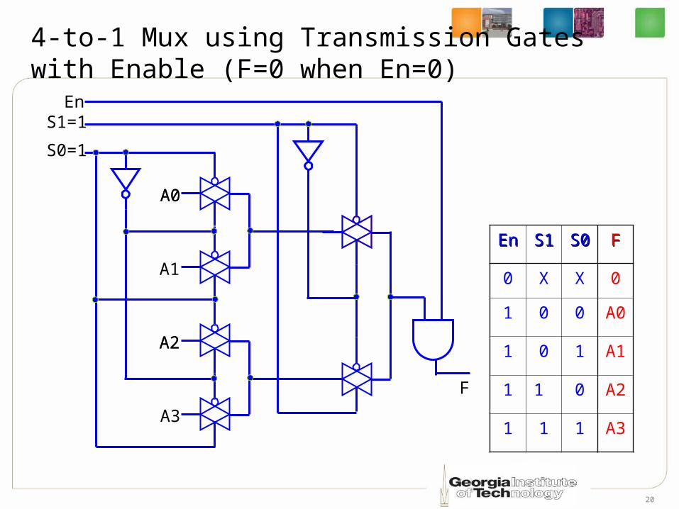
4-to-1 Mux using Transmission Gates with Enable (F=0 when En=0)
A0
A1
A2
A3
A0
A2
S0=1
S1=1
EnEn S1S1 S0S0 FF
0 X X 0
1 0 0 A0
1 0 1 A1
1 1 0 A2
1 1 1 A3
F
En
21
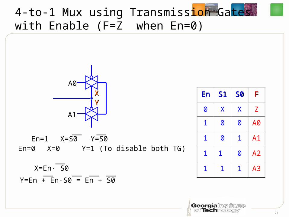
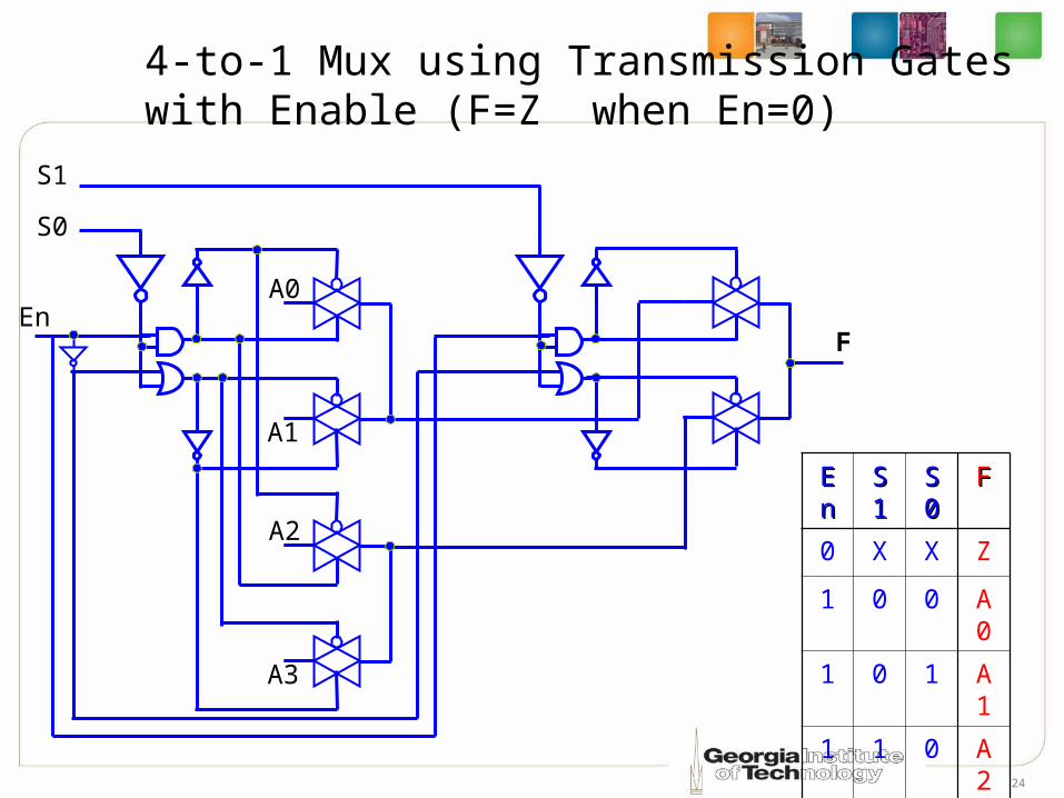
4-to-1 Mux using Transmission Gates with Enable (F=Z when En=0)
A0
A1
EnEn S1S1 S0S0 FF
0 X X Z
1 0 0 A0
1 0 1 A1
1 1 0 A2
1 1 1 A3
En=0 X=0 Y=1 (To disable both TG)
XXYY
X=En· S0
En=1 X=S0 Y=S0
Y=En + En·S0 = En + S0
22
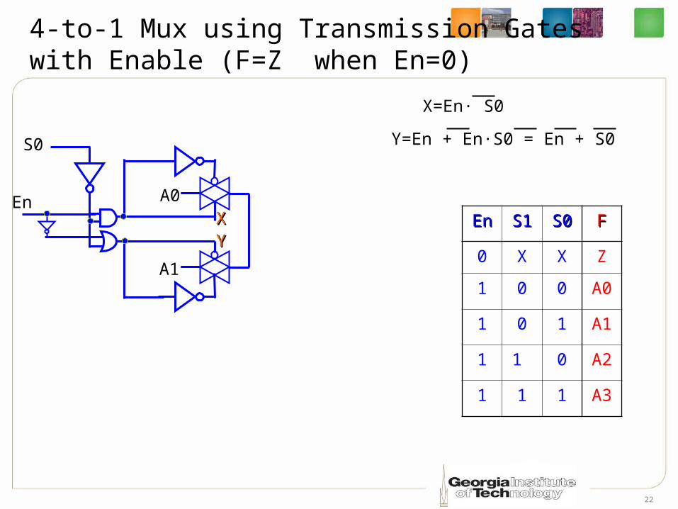
4-to-1 Mux using Transmission Gates with Enable (F=Z when En=0)
A0
A1
EnEn S1S1 S0S0 FF
0 X X Z
1 0 0 A0
1 0 1 A1
1 1 0 A2
1 1 1 A3
XXYY
X=En· S0
En
S0 Y=En + En·S0 = En + S0
XXYY
23
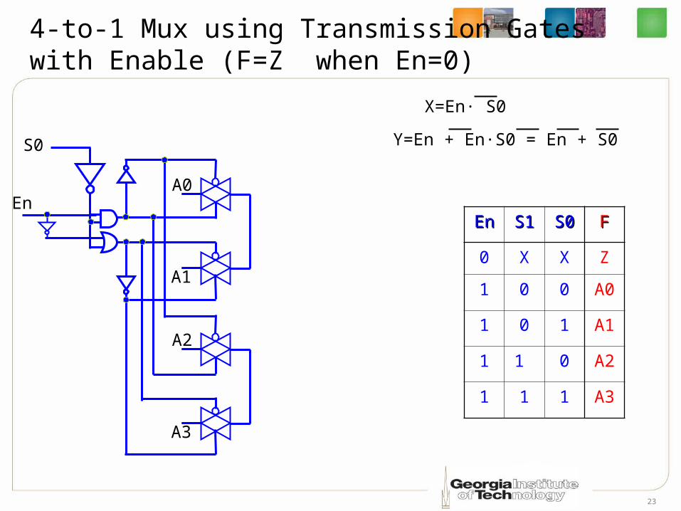
4-to-1 Mux using Transmission Gates with Enable (F=Z when En=0)
A0
A1
EnEn S1S1 S0S0 FF
0 X X Z
1 0 0 A0
1 0 1 A1
1 1 0 A2
1 1 1 A3
X=En· S0
En
S0
A2
A3
Y=En + En·S0 = En + S0
24
4-to-1 Mux using Transmission Gates with Enable (F=Z when En=0)
A0
A1
En
S0
A2
A3
F
EEnn
SS11
SS00
FF
0 X X Z
1 0 0 A0
1 0 1 A1
1 1 0 A2
1 1 1 A3
S1
25
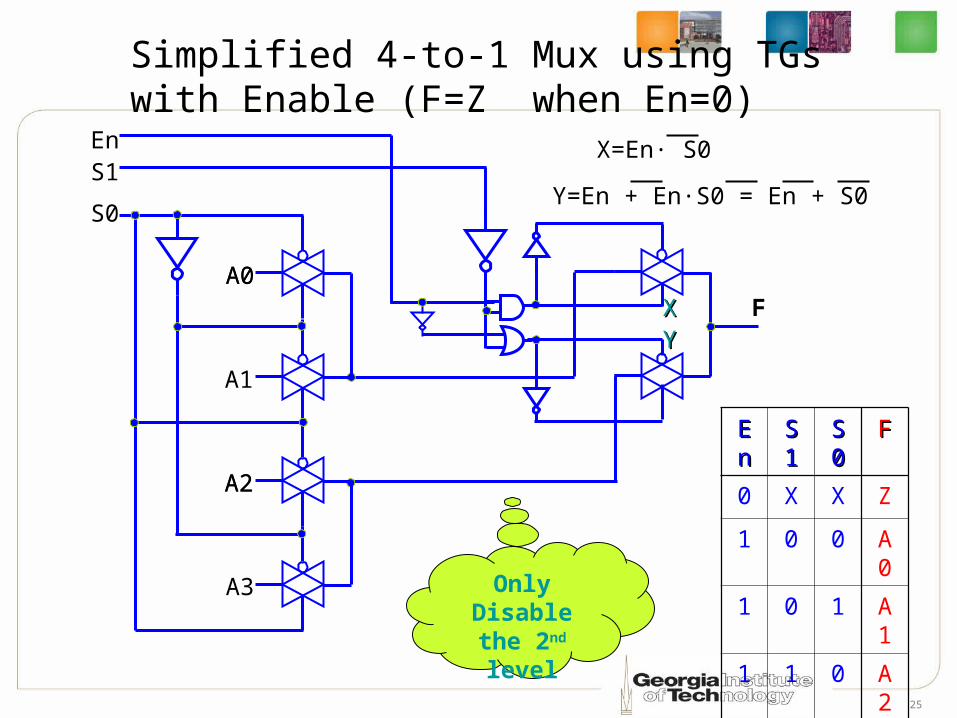
Simplified 4-to-1 Mux using TGs with Enable (F=Z when En=0)
S1
F
EEnn
SS11
SS00
FF
0 X X Z
1 0 0 A0
1 0 1 A1
1 1 0 A2
1 1 1 A3
A0
A1
A2
A3
A0
A2
S0
En
Only Disable the 2nd level
X=En· S0
XXYY
Y=En + En·S0 = En + S0
26
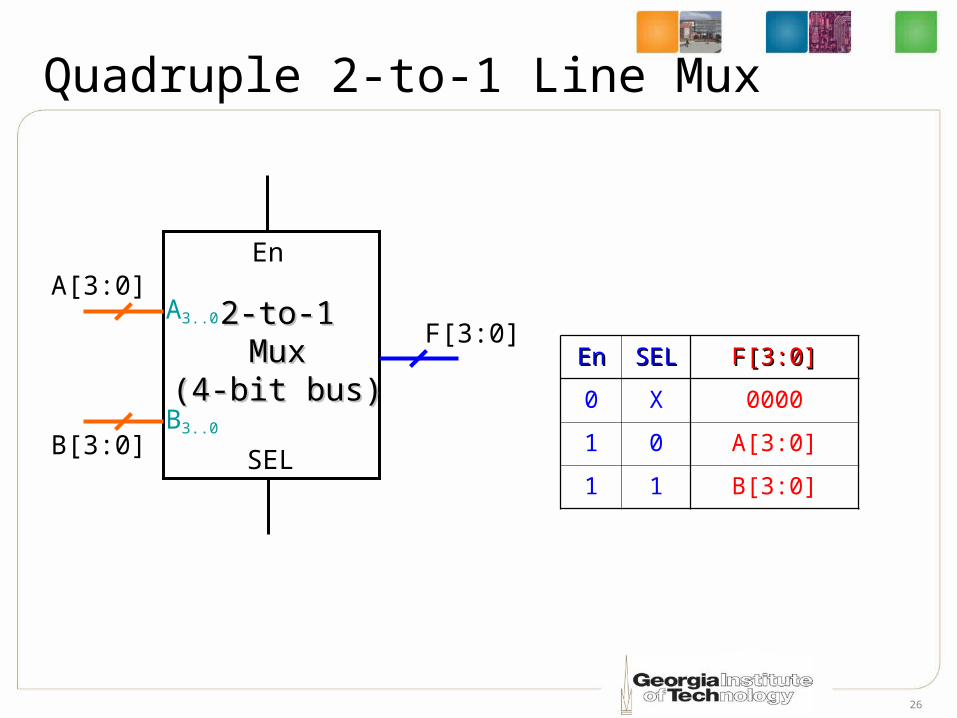
Quadruple 2-to-1 Line Mux
F[3:0]
SEL
En
2-to-12-to-1MuxMux
(4-bit bus)(4-bit bus)
A3..0
B3..0
A[3:0]
B[3:0]
EnEn SELSEL F[3:0]F[3:0]
0 X 0000
1 0 A[3:0]
1 1 B[3:0]
27
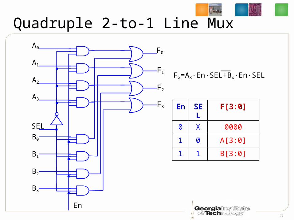
Quadruple 2-to-1 Line Mux
EnEn SESELL
F[3:0]F[3:0]
0 X 0000
1 0 A[3:0]
1 1 B[3:0]
SEL
B0
A0 F0
B3
A3
F3
B1
A1
F1
B2
A2
F2
En
Fx=Ax·En·SEL+Bx·En·SEL
28
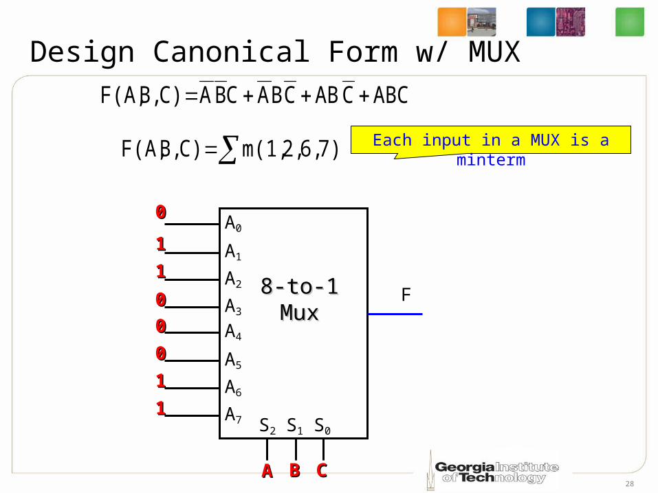
Design Canonical Form w/ MUX
7) 6, 2, m(1,C)B,F(A,
ABCCABCBACBAC)B,F(A,
F
A0
A1
A2
A3
S1 S0
8-to-18-to-1MuxMux
S2
A4
A5
A6
A7
00
00
00
00
11
11
11
11
Each input in a MUX is a minterm
AA BB CC
29
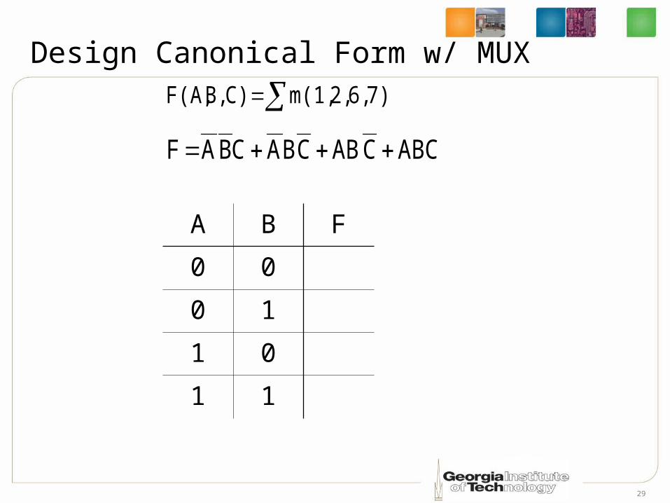
Design Canonical Form w/ MUX
7) 6, 2, m(1,C)B,F(A,
ABCCABCBACBAF
A B F
0 0
0 1
1 0
1 1
30
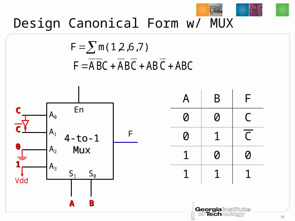
Design Canonical Form w/ MUX
7) 6, 2, m(1,F
ABCCABCBACBAF
A B F
0 0 C
0 1 C
1 0 0
1 1 1
F
A0
A1
A2
A3S1 S0
En
4-to-14-to-1MuxMux
AA BB
CC
CC
00
11
Vdd
31
Design Canonical Form w/ MUX
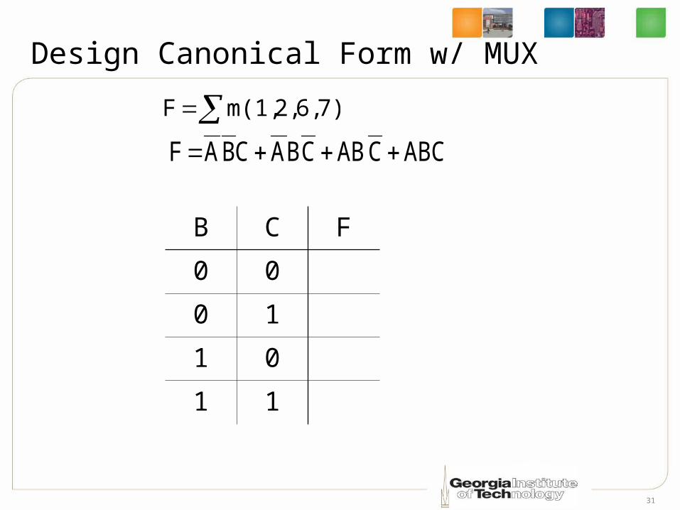
7) 6, 2, m(1,F
ABCCABCBACBAF
B C F
0 0
0 1
1 0
1 1
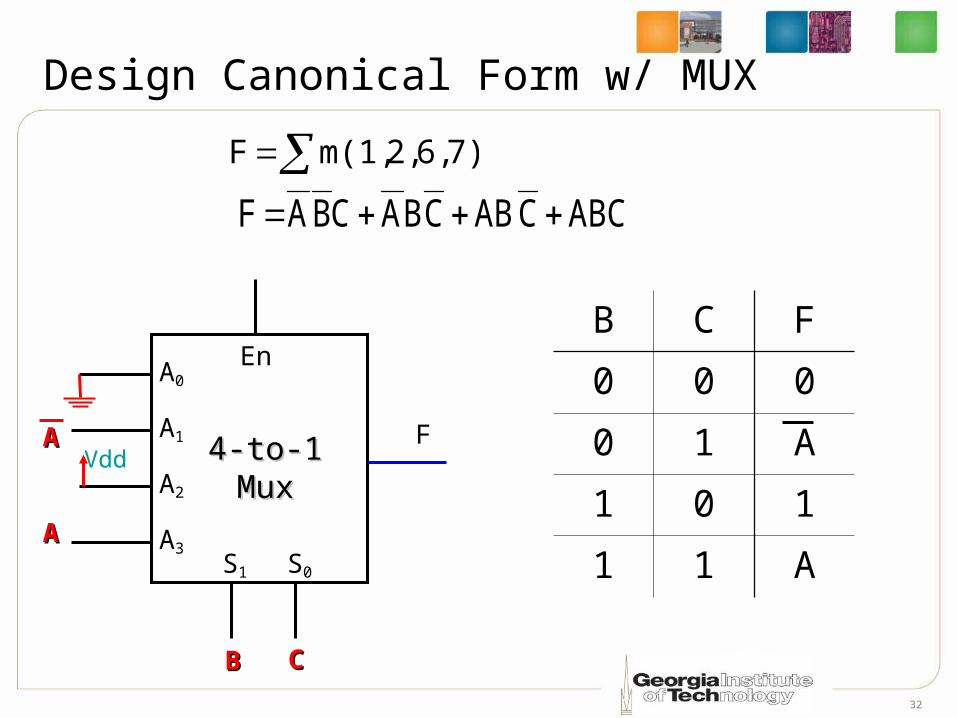
32
Design Canonical Form w/ MUX
7) 6, 2, m(1,F
ABCCABCBACBAF
B C F
0 0 0
0 1 A
1 0 1
1 1 A
F
A0
A1
A2
A3S1 S0
En
4-to-14-to-1MuxMux
BB CC
AA
AA
Vdd
33
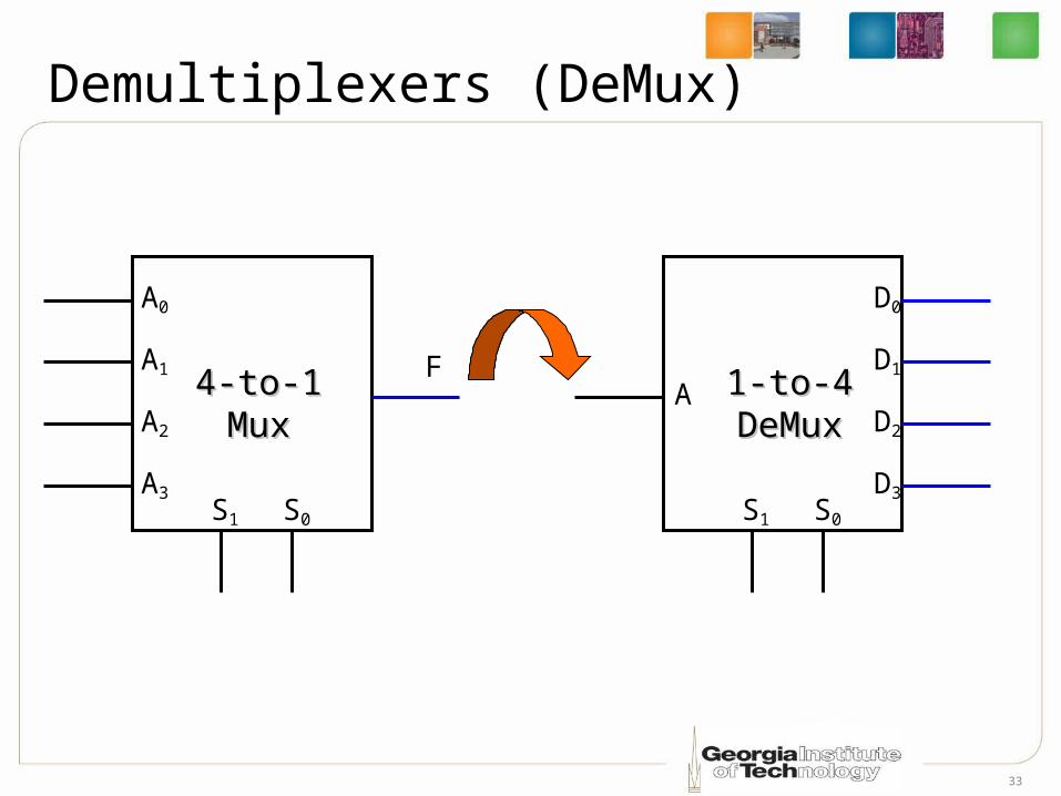
Demultiplexers (DeMux)
F
A0
A1
A2
A3S1 S0
4-to-14-to-1MuxMux
A
D0
D1
D2
D3S1 S0
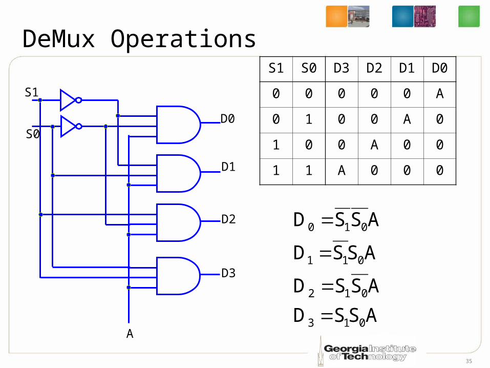
1-to-41-to-4DeMuxDeMux
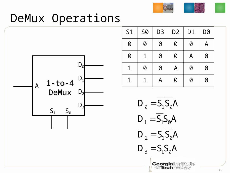
34
DeMux OperationsS1 S0 D3 D2 D1 D0
0 0 0 0 0 A
0 1 0 0 A 0
1 0 0 A 0 0
1 1 A 0 0 0A
D0
D1
D2
D3S1 S0
1-to-41-to-4DeMuxDeMux
ASSD
ASSD
ASSD
ASSD
013
012
011
010
35
DeMux OperationsS1 S0 D3 D2 D1 D0
0 0 0 0 0 A
0 1 0 0 A 0
1 0 0 A 0 0
1 1 A 0 0 0
ASSD
ASSD
ASSD
ASSD
013
012
011
010
D0
D1
D2
D3
A
S1
S0
36
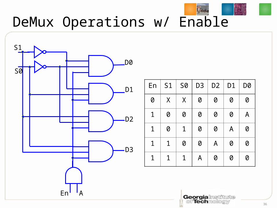
DeMux Operations w/ Enable
En S1 S0 D3 D2 D1 D0
0 X X 0 0 0 0
1 0 0 0 0 0 A
1 0 1 0 0 A 0
1 1 0 0 A 0 0
1 1 1 A 0 0 0
D0
D1
D2
D3
A
S1
S0
En
Recommended