Embed Size (px)
Citation preview

LOGO รหัสวิชา 353152 วงจรอิเล็กทรอนิกส์ 1
DIODES AND APPLICATIONS
1
บทท่ี 2
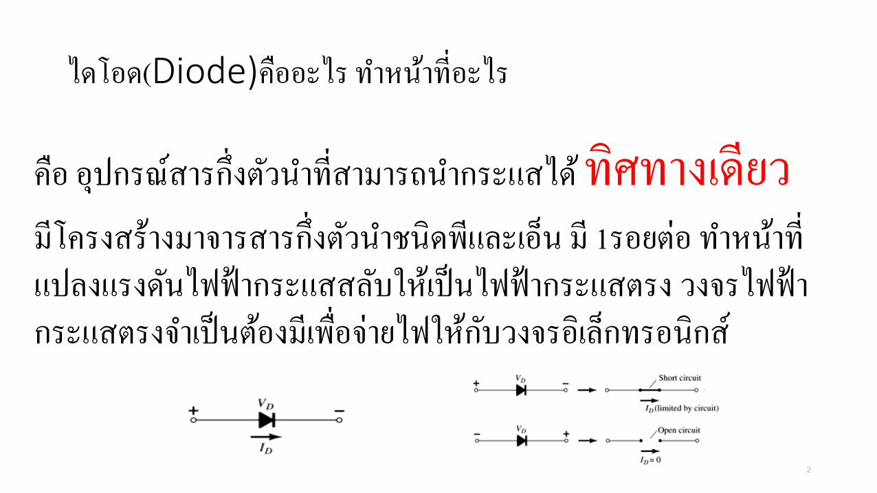
ไดโอด(Diode)คืออะไร ท ำหนำ้ท่ีอะไร
คือ อุปกรณ์สำรก่ึงตวัน ำท่ีสำมำรถน ำกระแสได ้ทิศทำงเดียวมีโครงสร้ำงมำจำรสำรก่ึงตวัน ำชนิดพแีละเอน็ มี 1รอยต่อ ท ำหนำ้ท่ีแปลงแรงดนัไฟฟ้ำกระแสสลบัใหเ้ป็นไฟฟ้ำกระแสตรง วงจรไฟฟ้ำกระแสตรงจ ำเป็นตอ้งมีเพือ่จ่ำยไฟใหก้บัวงจรอิเลก็ทรอนิกส์
2
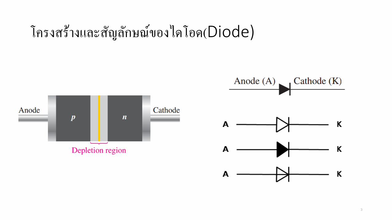
โครงสร้ำงและสัญลกัษณ์ของไดโอด(Diode)
3
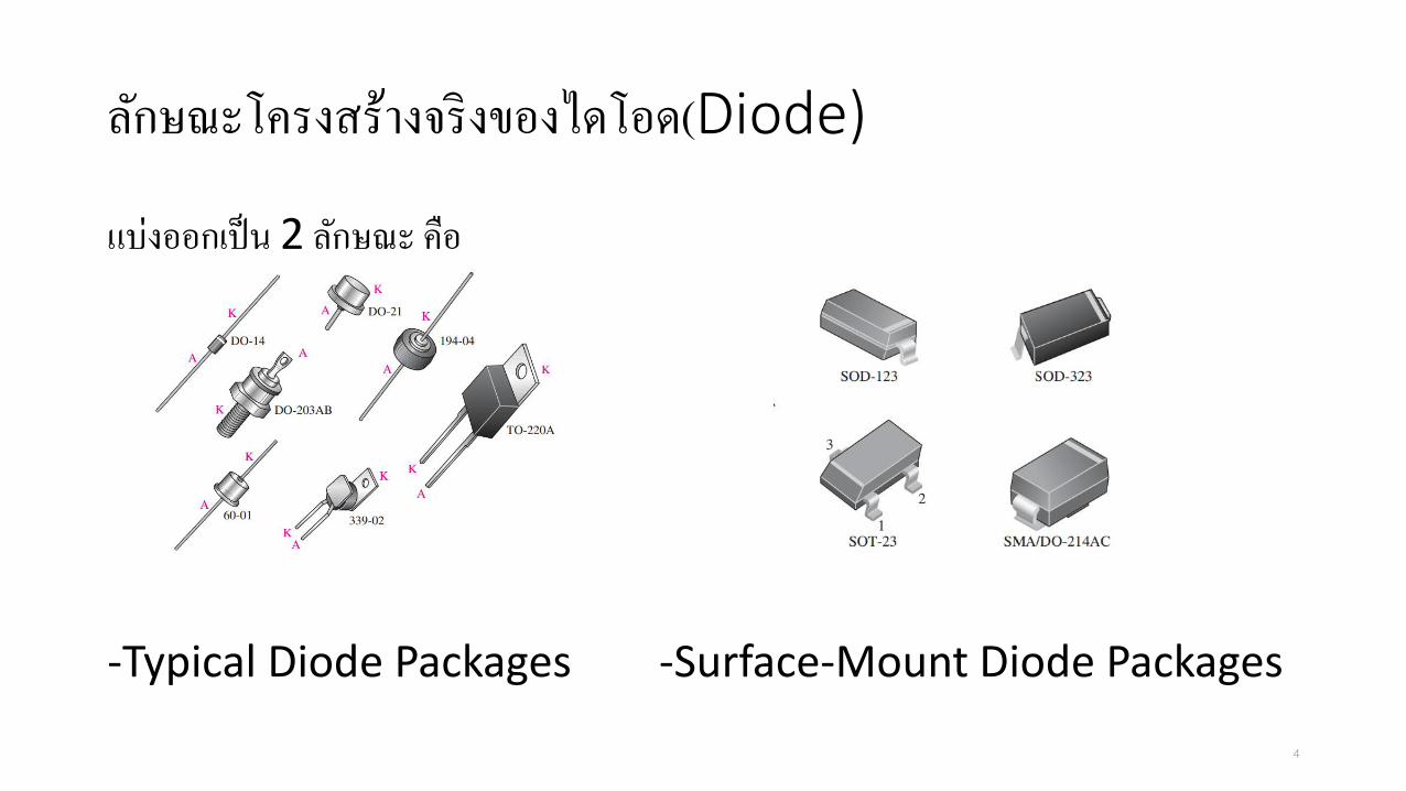
ลกัษณะโครงสร้ำงจริงของไดโอด(Diode)
แบ่งออกเป็น 2 ลกัษณะ คือ
-Typical Diode Packages -Surface-Mount Diode Packages
4
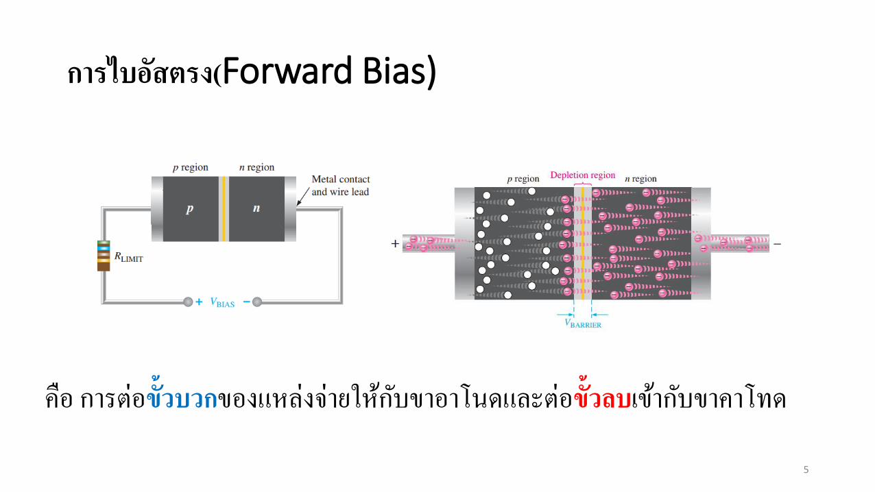
การไบอสัตรง(Forward Bias)
5
คือ กำรต่อขั้วบวกของแหล่งจ่ำยใหก้บัขำอำโนดและต่อขั้วลบเขำ้กบัขำคำโทด
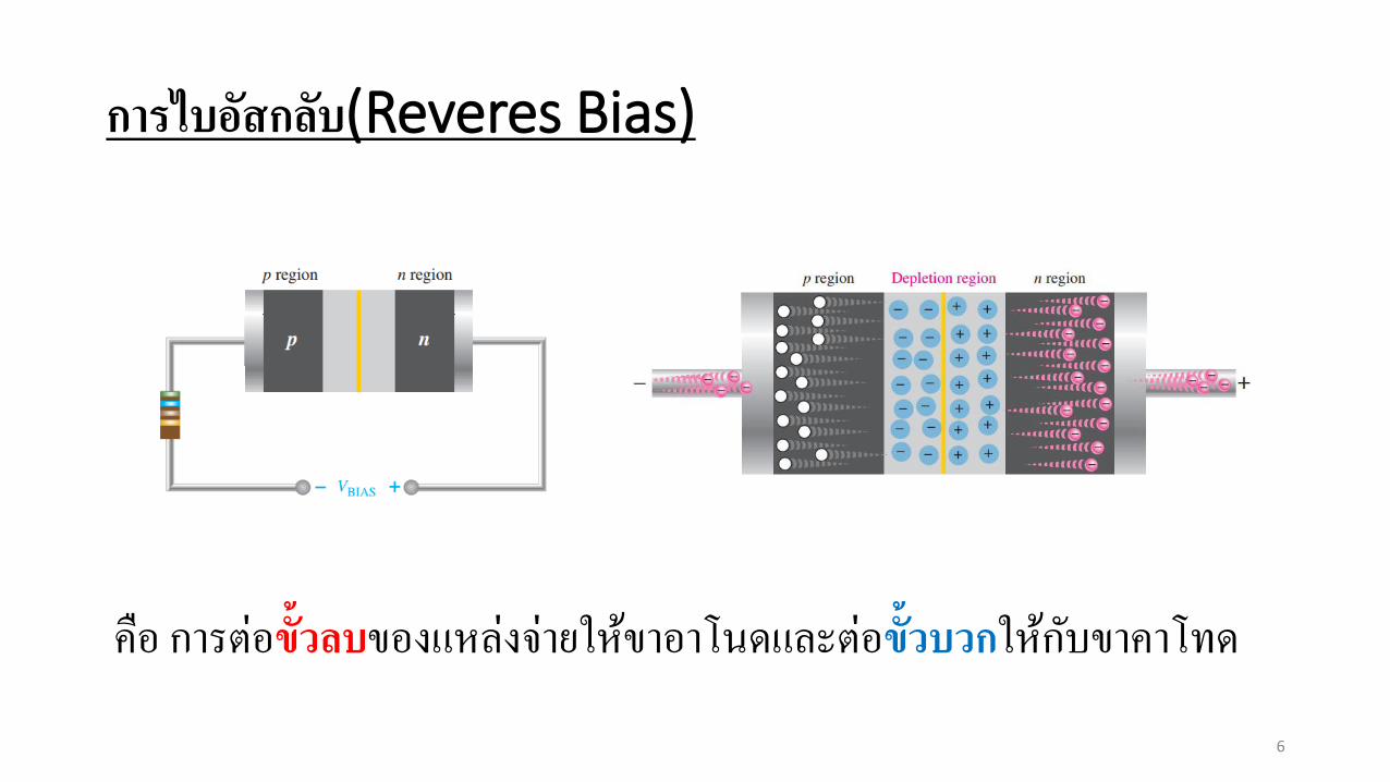
การไบอสักลบั(Reveres Bias)
6
คือ กำรต่อขั้วลบของแหล่งจ่ำยใหข้ำอำโนดและต่อขั้วบวกใหก้บัขำคำโทด
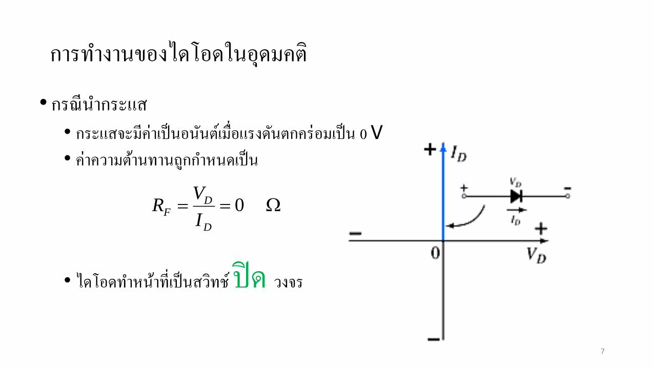
กำรท ำงำนของไดโอดในอุดมคติ
• กรณีน ำกระแส• กระแสจะมีค่ำเป็นอนนัตเ์ม่ือแรงดนัตกคร่อมเป็น 0 V• ค่ำควำมตำ้นทำนถกูก ำหนดเป็น
• ไดโอดท ำหนำ้ท่ีเป็นสวิทช ์ปิด วงจร
7
0D
DF
I
VR
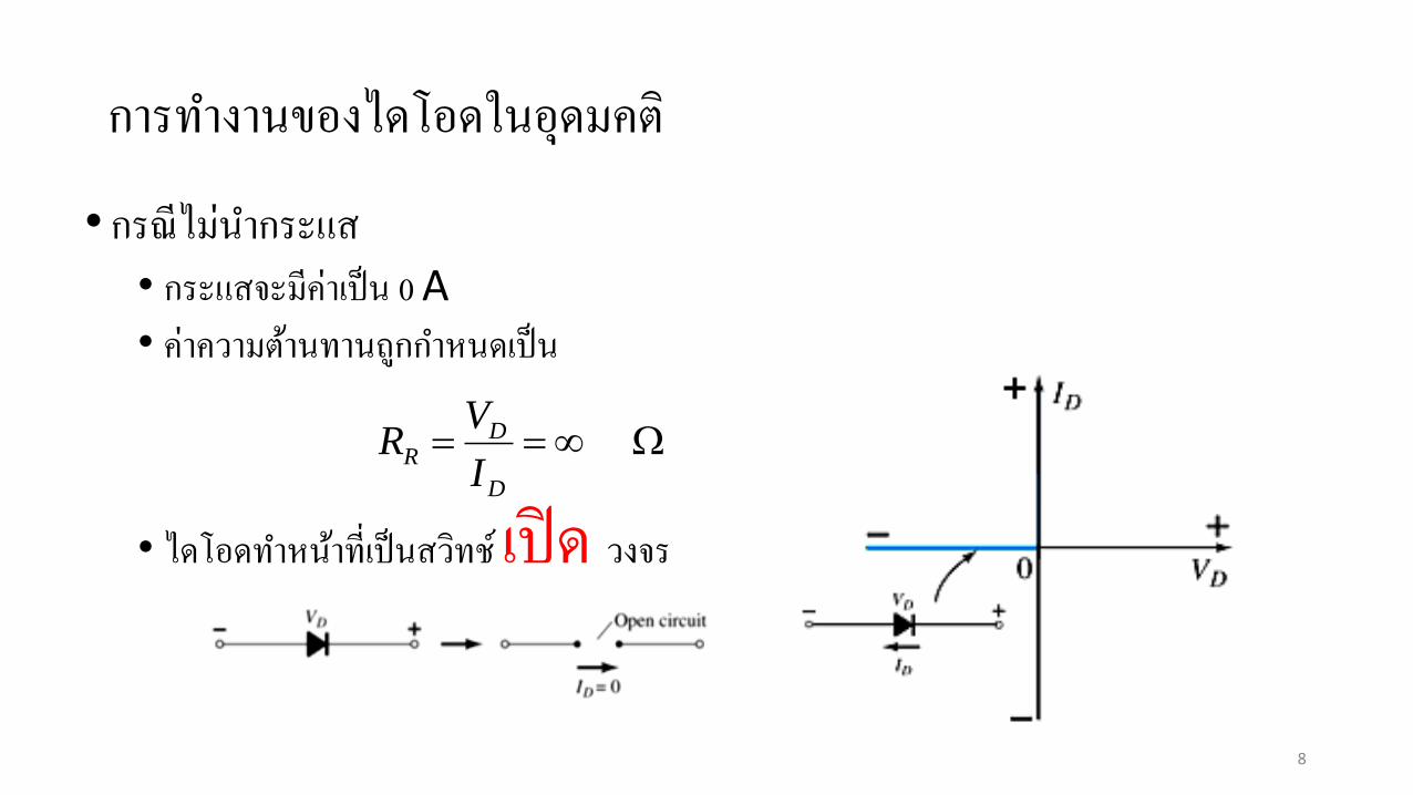
กำรท ำงำนของไดโอดในอุดมคติ
• กรณีไม่น ำกระแส• กระแสจะมีค่ำเป็น 0 A• ค่ำควำมตำ้นทำนถกูก ำหนดเป็น
• ไดโอดท ำหนำ้ท่ีเป็นสวิทช ์เปิด วงจร
8
D
DR
I
VR
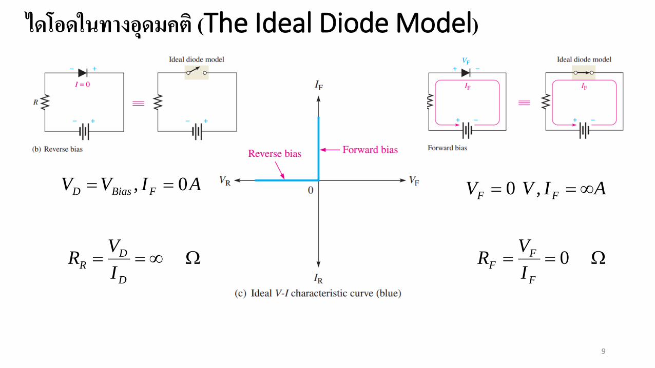
ไดโอดในทางอุดมคต ิ(The Ideal Diode Model)
9
0F
FF
I
VR
AIVV FF , 0
D
DR
I
VR
AIVV FBiasD 0,
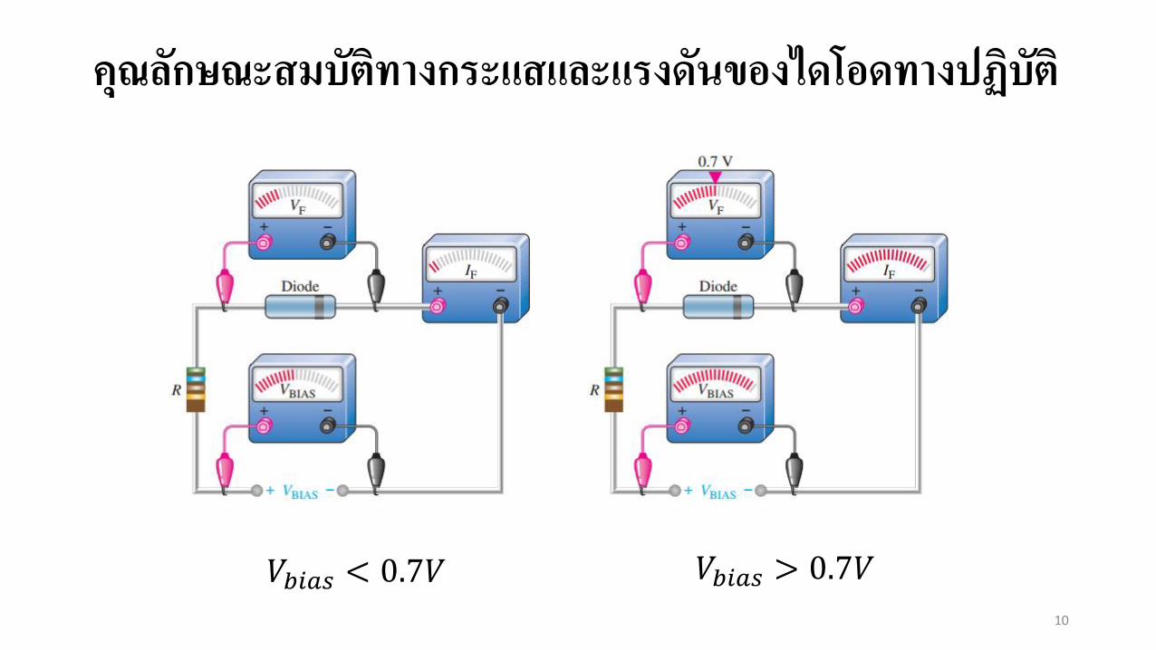
คุณลกัษณะสมบตัทิางกระแสและแรงดนัของไดโอดทางปฏิบตัิ
10
𝑉𝑏𝑖𝑎𝑠 < 0.7𝑉 𝑉𝑏𝑖𝑎𝑠 > 0.7𝑉
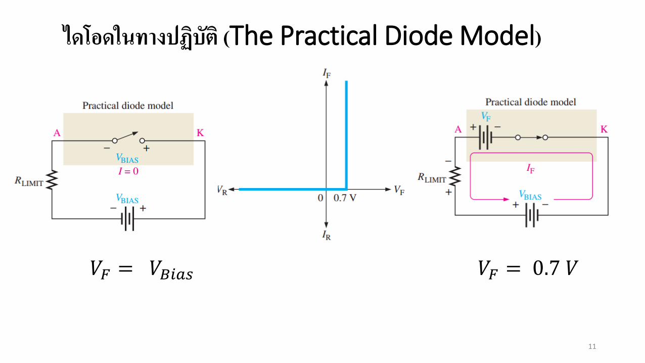
ไดโอดในทางปฏิบตั ิ(The Practical Diode Model)
11
𝑉𝐹 = 0.7 𝑉𝑉𝐹 = 𝑉𝐵𝑖𝑎𝑠
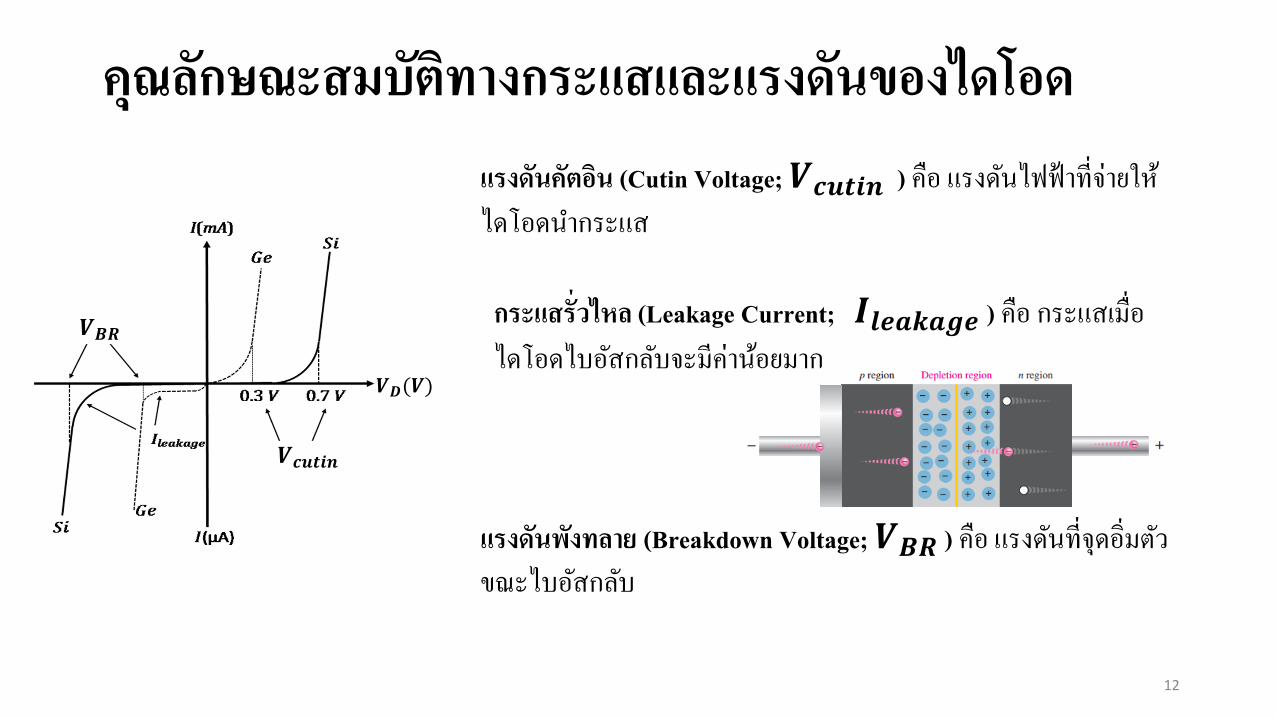
คุณลกัษณะสมบตัทิางกระแสและแรงดนัของไดโอด
12
แรงดันคัตอิน (Cutin Voltage; 𝑽𝒄𝒖𝒕𝒊𝒏 ) คือ แรงดนัไฟฟ้ำท่ีจ่ำยให้ไดโอดน ำกระแส
กระแสร่ัวไหล (Leakage Current; 𝑰𝒍𝒆𝒂𝒌𝒂𝒈𝒆 ) คือ กระแสเม่ือไดโอดไบอสักลบัจะมีค่ำนอ้ยมำก
แรงดันพงัทลาย (Breakdown Voltage; 𝑽𝑩𝑹 ) คือ แรงดนัท่ีจุดอ่ิมตวัขณะไบอสักลบั
𝑽𝒄𝒖𝒕𝒊𝒏
𝑽𝑩𝑹
𝑽𝑫(𝑽)
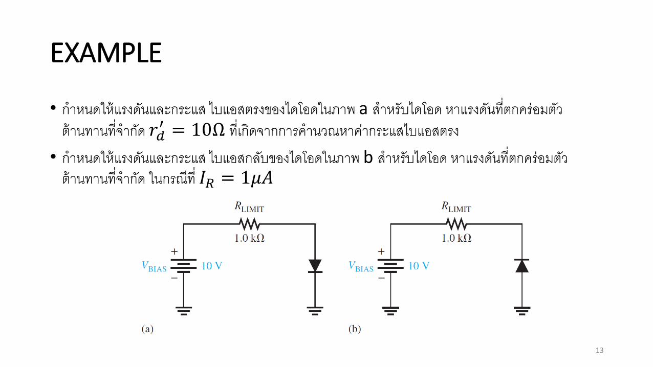
EXAMPLE
• ก ำหนดให้แรงดนัและกระแส ไบแอสตรงของไดโอดในภำพ a ส ำหรับไดโอด หำแรงดนัที่ตกคร่อมตวัต้ำนทำนที่จ ำกดั 𝑟𝑑
′ = 10Ω ที่เกิดจำกกำรค ำนวณหำคำ่กระแสไบแอสตรง• ก ำหนดให้แรงดนัและกระแส ไบแอสกลบัของไดโอดในภำพ b ส ำหรับไดโอด หำแรงดนัที่ตกคร่อมตวัต้ำนทำนที่จ ำกดั ในกรณีที่ 𝐼𝑅 = 1𝜇𝐴
13
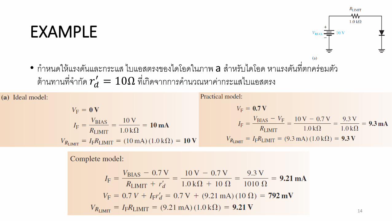
EXAMPLE
• ก ำหนดให้แรงดนัและกระแส ไบแอสตรงของไดโอดในภำพ a ส ำหรับไดโอด หำแรงดนัที่ตกคร่อมตวัต้ำนทำนที่จ ำกดั 𝑟𝑑
′ = 10Ω ที่เกิดจำกกำรค ำนวณหำคำ่กระแสไบแอสตรง
14
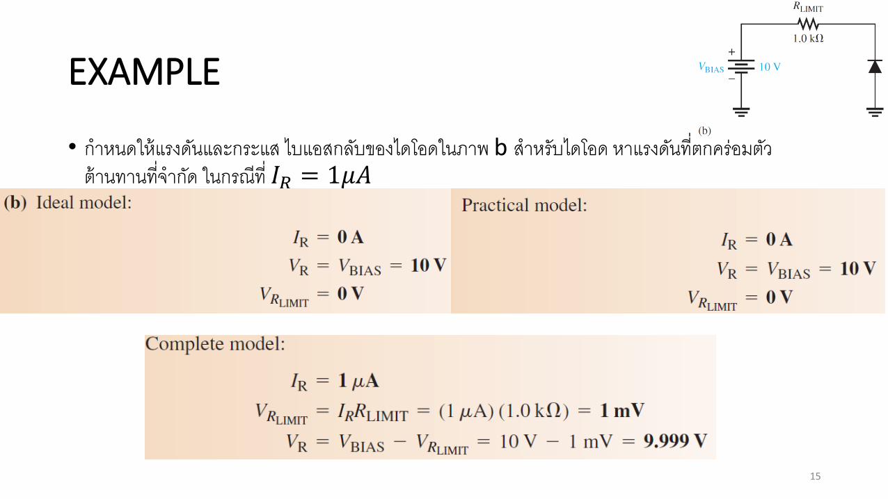
EXAMPLE
• ก ำหนดให้แรงดนัและกระแส ไบแอสกลบัของไดโอดในภำพ b ส ำหรับไดโอด หำแรงดนัที่ตกคร่อมตวัต้ำนทำนที่จ ำกดั ในกรณีที่ 𝐼𝑅 = 1𝜇𝐴
15
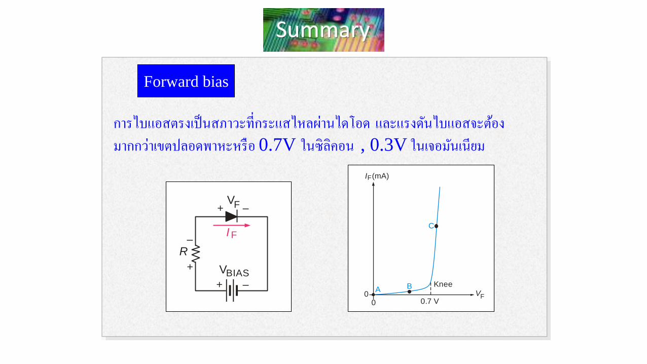
Summary
Forward bias
กำรไบแอสตรงเป็นสภำวะท่ีกระแสไหลผำ่นไดโอด และแรงดนัไบแอสจะตอ้งมำกกวำ่เขตปลอดพำหะหรือ 0.7V ในซิลิคอน , 0.3V ในเจอมนัเนียม
R
I F
BIAS
V–+
–+
+
–
F
V
B
0.7 V
C
A
00
Knee
VF
IF (mA)
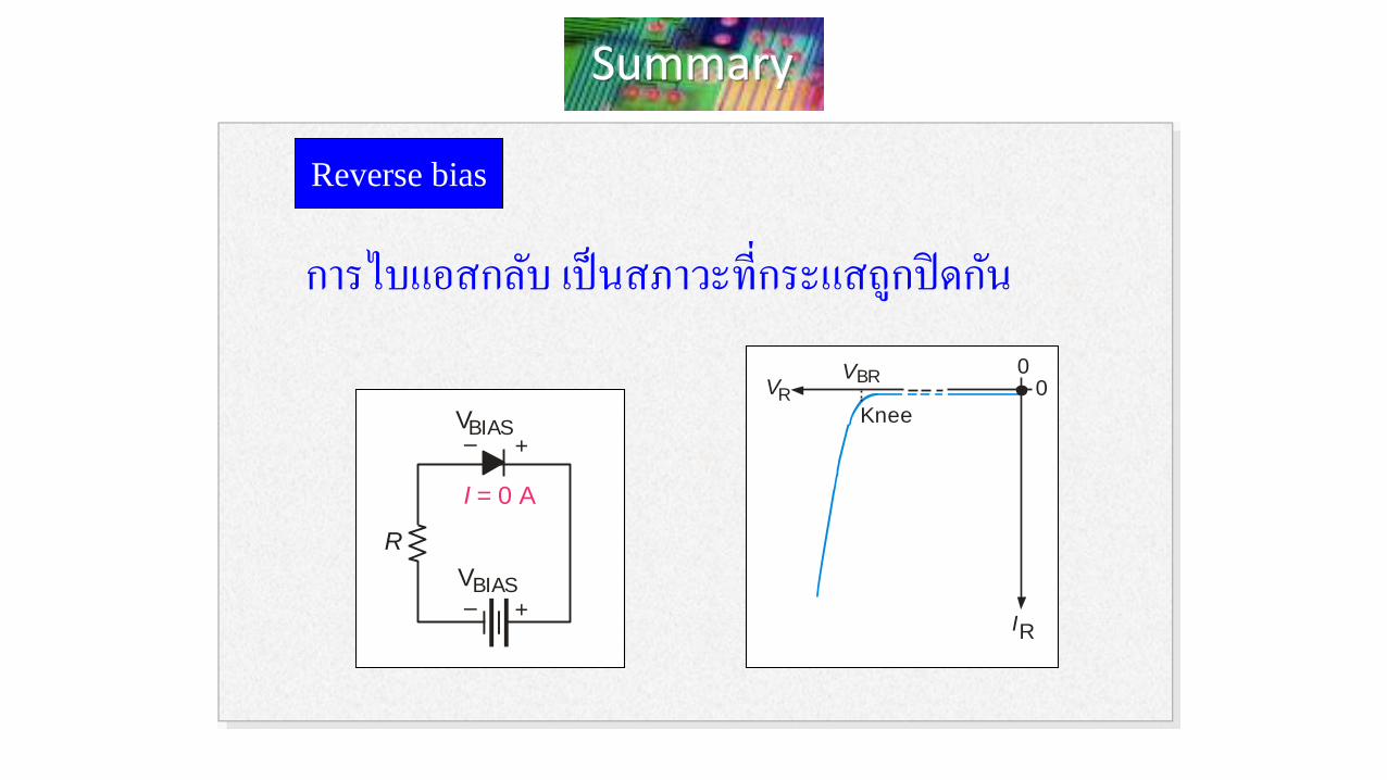
Summary
Reverse bias
กำรไบแอสกลบั เป็นสภำวะท่ีกระแสถูกปิดกนั
R
BIAS
BIAS
I = 0 A
– +
– +
V
V
00
Knee
VR
IR
VBR
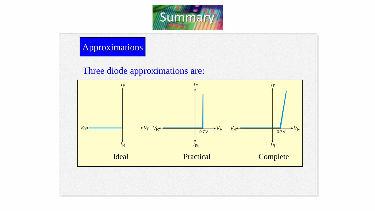
Summary
Approximations
Three diode approximations are:
VR
IR
VF
IF
0.7 VVR
IR
VF
IF
0.7 VVR
IR
VF
IF
Ideal Practical Complete
Summary
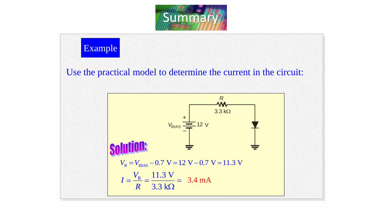
Example
Use the practical model to determine the current in the circuit:
12 V–
+
R
3.3 k
VBIAS
BIAS 0.7 V 12 V 0.7 V 11.3 VRV V
R 11.3 V
3.3 k
VI
R
3.4 mA
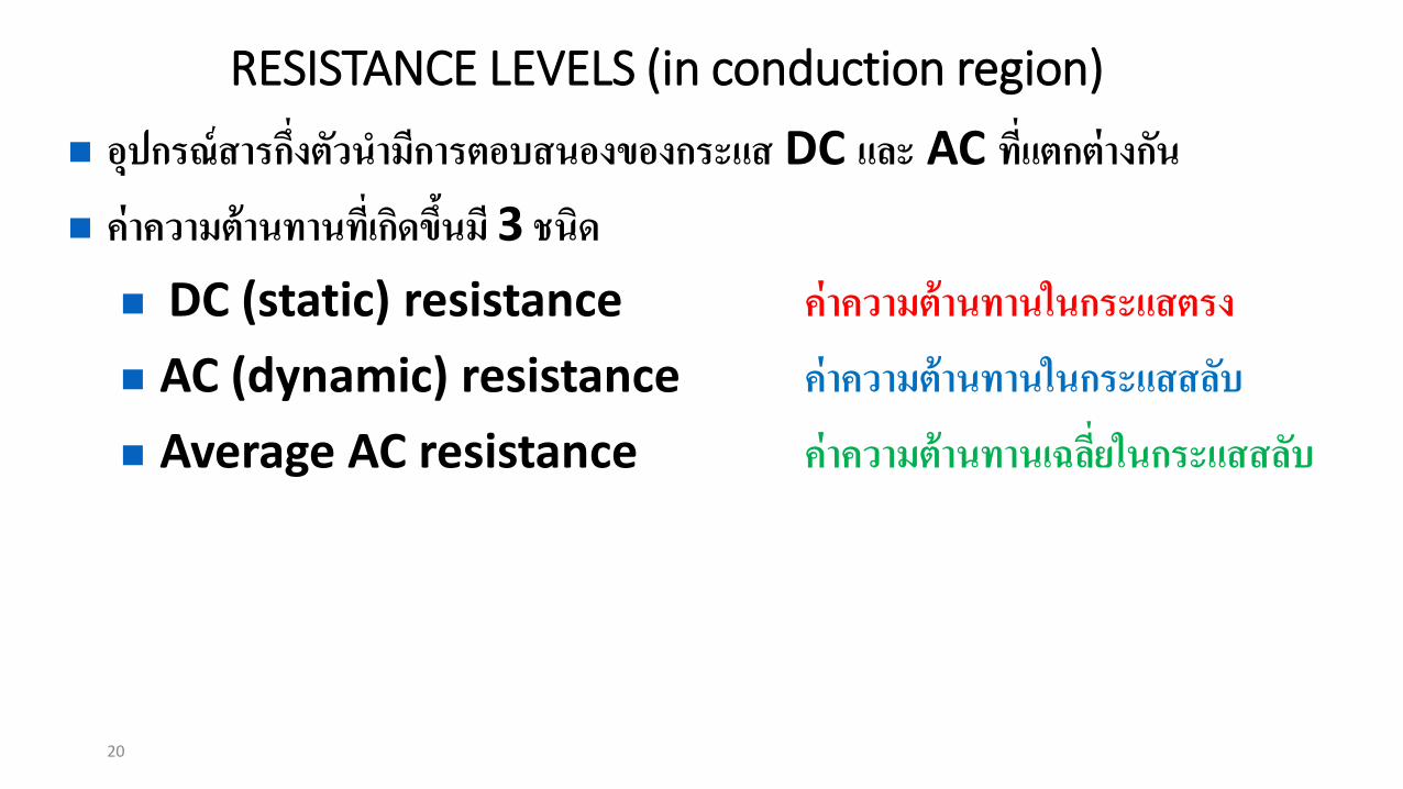
RESISTANCE LEVELS (in conduction region)
20
อุปกรณ์สารกึง่ตวัน ามกีารตอบสนองของกระแส DC และ AC ที่แตกต่างกนั
ค่าความต้านทานทีเ่กดิขึน้ม ี3 ชนิด
DC (static) resistance ค่าความต้านทานในกระแสตรง
AC (dynamic) resistance ค่าความต้านทานในกระแสสลบั
Average AC resistance ค่าความต้านทานเฉลีย่ในกระแสสลบั
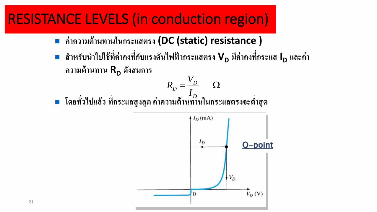
RESISTANCE LEVELS (in conduction region)
ค่าความต้านทานในกระแสตรง (DC (static) resistance )
ส าหรับน าไปใช้ท่ีค่าคงท่ีกับแรงดันไฟฟ้ากระแสตรง VD มีค่าคงท่ีกระแส ID และค่าความต้านทาน RD ดังสมการ
โดยท่ัวไปแล้ว ท่ีกระแสสูงสุด ค่าความต้านทานในกระแสตรงจะต ่าสุด
21
Q-point
D
DD
I
VR
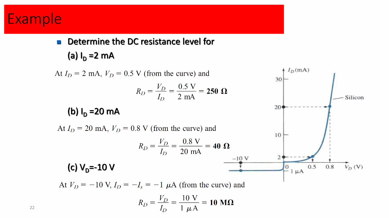
Example
Determine the DC resistance level for
(a) ID =2 mA
(b) ID =20 mA
(c) VD=-10 V
22
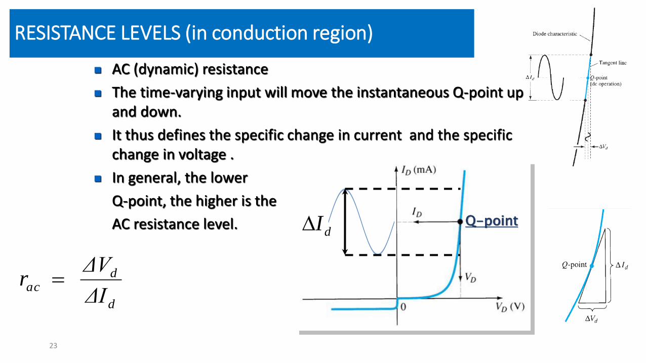
RESISTANCE LEVELS (in conduction region)
AC (dynamic) resistance
The time-varying input will move the instantaneous Q-point up and down.
It thus defines the specific change in current and the specific change in voltage .
In general, the lower
Q-point, the higher is the
AC resistance level.
23
Q-point
d
dac
ΔI
ΔV r
dI
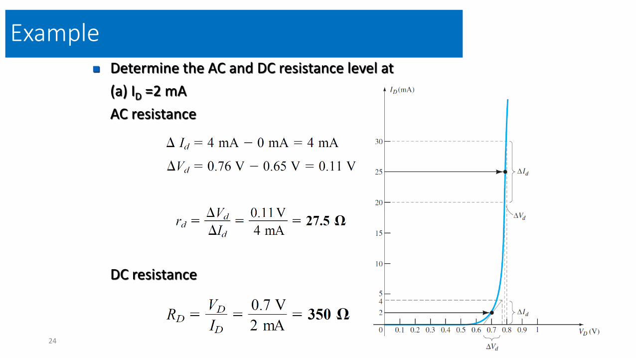
Example Determine the AC and DC resistance level at
(a) ID =2 mA
AC resistance
DC resistance
24
Example
25
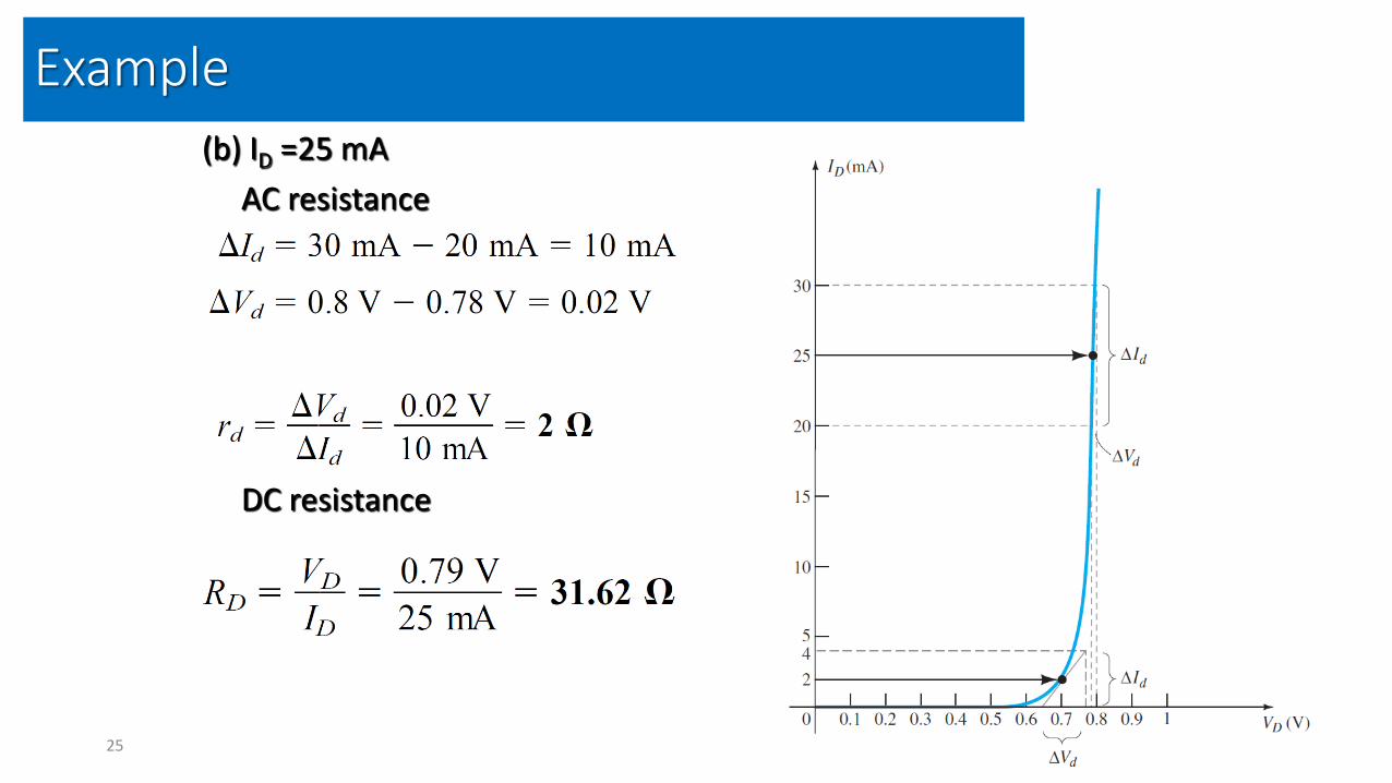
(b) ID =25 mA
AC resistance
DC resistance
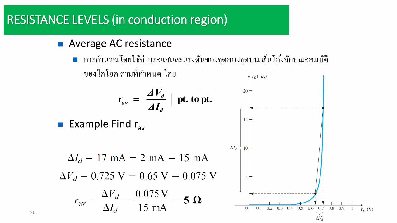
RESISTANCE LEVELS (in conduction region)
Average AC resistance
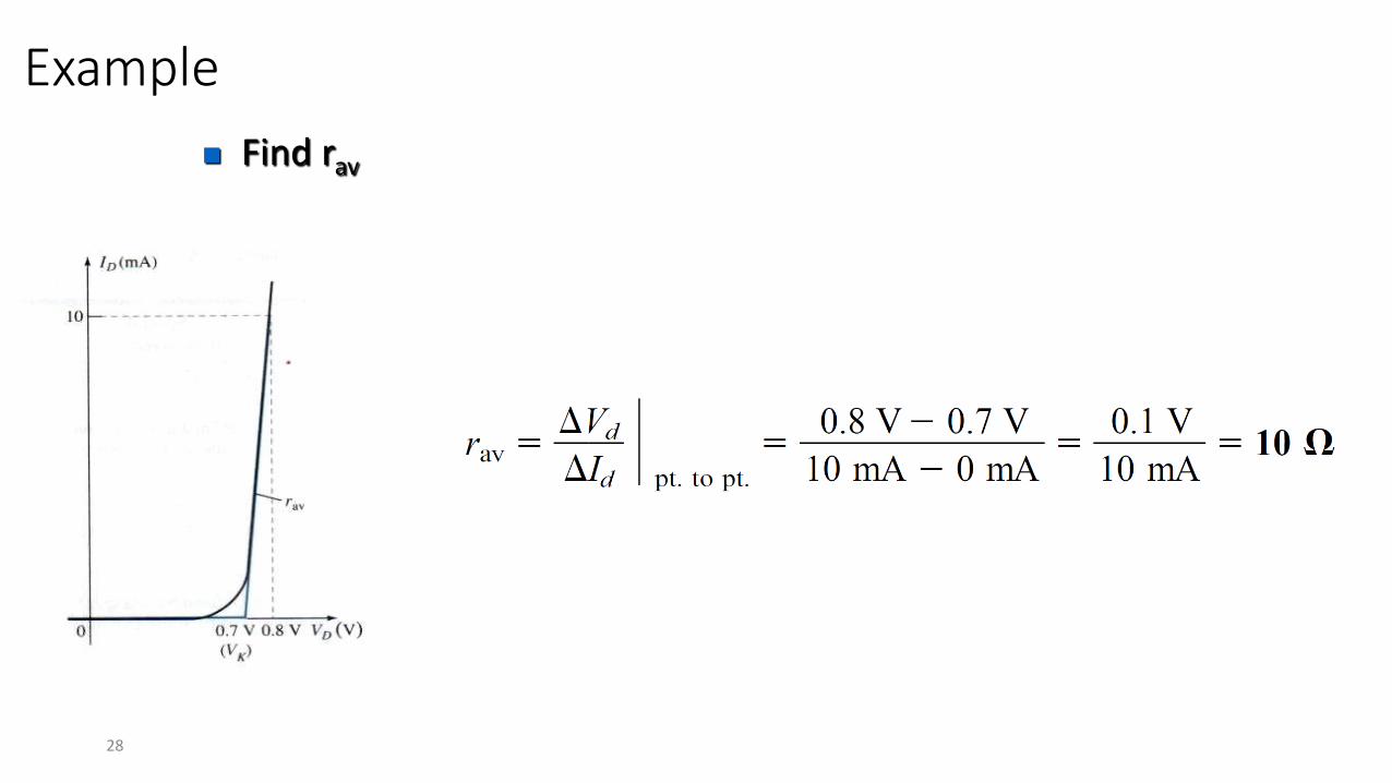
กำรค ำนวณโดยใชค้่ำกระแสและแรงดนัของจุดสองจุดบนเส้นโคง้ลกัษณะสมบติัของไดโอด ตำมท่ีก ำหนด โดย
Example Find rav
26
pt. to pt. d
dav
ΔI
ΔV r
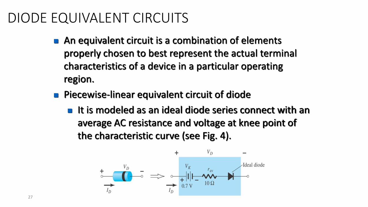
DIODE EQUIVALENT CIRCUITS
An equivalent circuit is a combination of elements properly chosen to best represent the actual terminal characteristics of a device in a particular operating region.
Piecewise-linear equivalent circuit of diode
It is modeled as an ideal diode series connect with an average AC resistance and voltage at knee point of the characteristic curve (see Fig. 4).
27
Example
Find rav
28
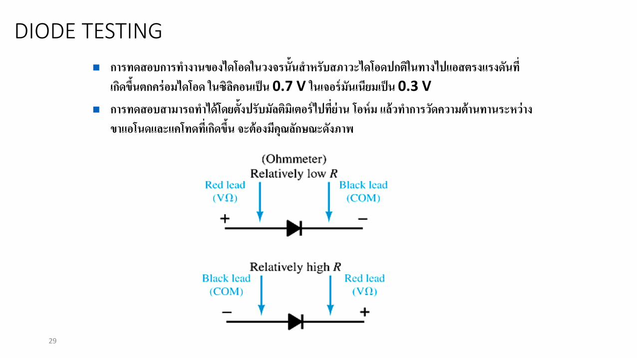
DIODE TESTING
การทดสอบการท างานของไดโอดในวงจรนั้นส าหรับสภาวะไดโอดปกตใินทางไปแอสตรงแรงดนัที่เกดิขึน้ตกคร่อมไดโอด ในซิลคิอนเป็น 0.7 V ในเจอร์มนัเนียมเป็น 0.3 V
การทดสอบสามารถท าได้โดยตั้งปรับมลัตมิเิตอร์ไปที่ย่าน โอห์ม แล้วท าการวดัความต้านทานระหว่างขาแอโนดและแคโทดที่เกดิขึน้ จะต้องมคุีณลกัษณะดงัภาพ
29
Quiz
1. A semiconductor is a crystalline material with
a. many free electrons held by the attraction of
positive ions
b. strong covalent bonds between neighboring atoms
c. only one electron in its outer shell
d. a filled valence shell

Quiz
2. A metallic conductor has
a. many free electrons held by the attraction of
positive ions
b. covalent bonds between neighboring atoms
c. four electrons in its outer shell
d. a filled valence shell
Quiz
3. In a semiconductor, the concept of an energy gap is
used to show the difference between the energies of the
a. nucleus and outer shell electrons
b. nucleus and the free electrons
c. conduction band electrons and valence electrons
d. core electrons and valence electrons

Quiz
4. An impurity such as Antimony (Sb) has five electrons
in its outer shell. When silicon has Sb impurities,
a. an n material is formed
b. the crystal will be negatively charged
c. both of the above
d. none of the above

Quiz
5. Compared to a p-material, the energy levels in an n-
material are
a. the same
b. greater
c. lower

Quiz
6. When a pn junction is formed, electrons move across
the junction and fill holes in the p-region. The filled hole
is a
a. neutral atom
b. minority carrier
c. positive ion
d. negative ion
Quiz
7. The forward biased knee voltage in a semiconductor
diode is approximately equal to the
a. bias supply voltage
b. breakdown voltage
c. output voltage
d. barrier potential
Quiz
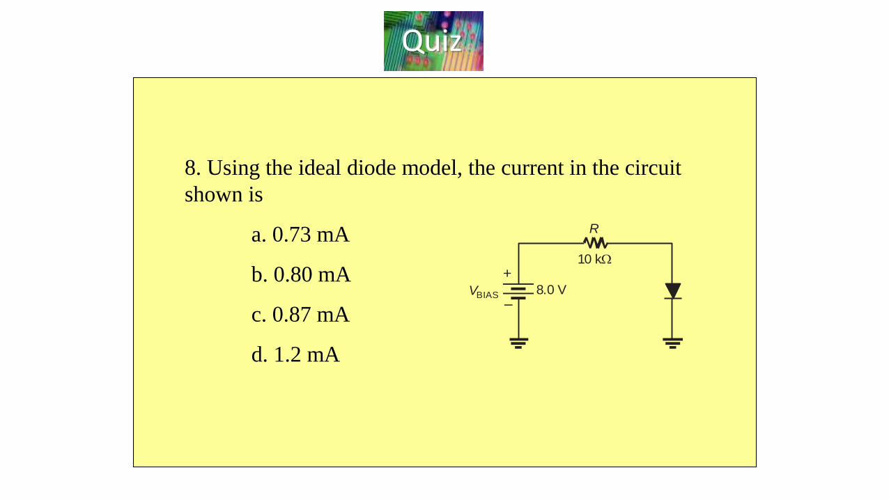
8. Using the ideal diode model, the current in the circuit
shown is
a. 0.73 mA
b. 0.80 mA
c. 0.87 mA
d. 1.2 mA
8.0 V –
+
R
10 k
VBIAS
Quiz
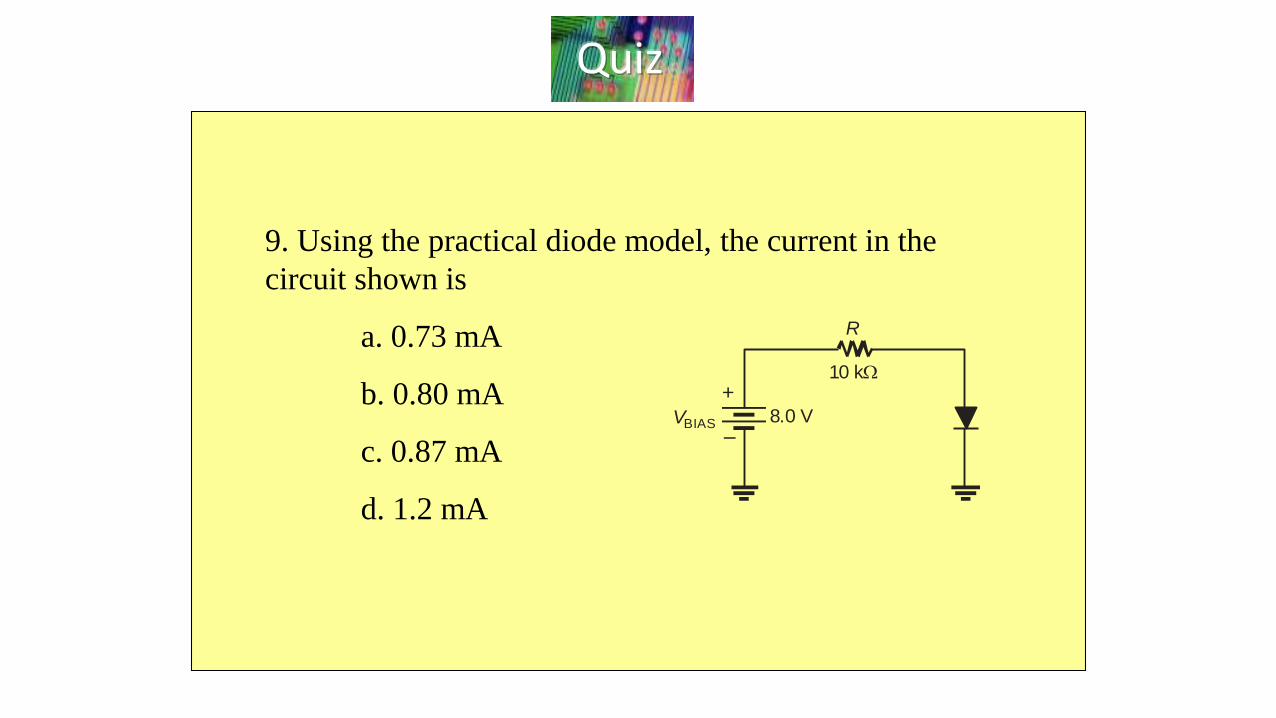
9. Using the practical diode model, the current in the
circuit shown is
a. 0.73 mA
b. 0.80 mA
c. 0.87 mA
d. 1.2 mA
8.0 V –
+
R
10 k
VBIAS
Quiz
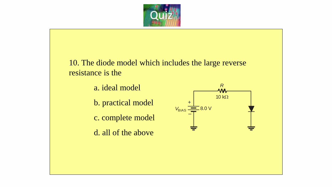
10. The diode model which includes the large reverse
resistance is the
a. ideal model
b. practical model
c. complete model
d. all of the above
8.0 V –
+
R
10 k
VBIAS
Quiz
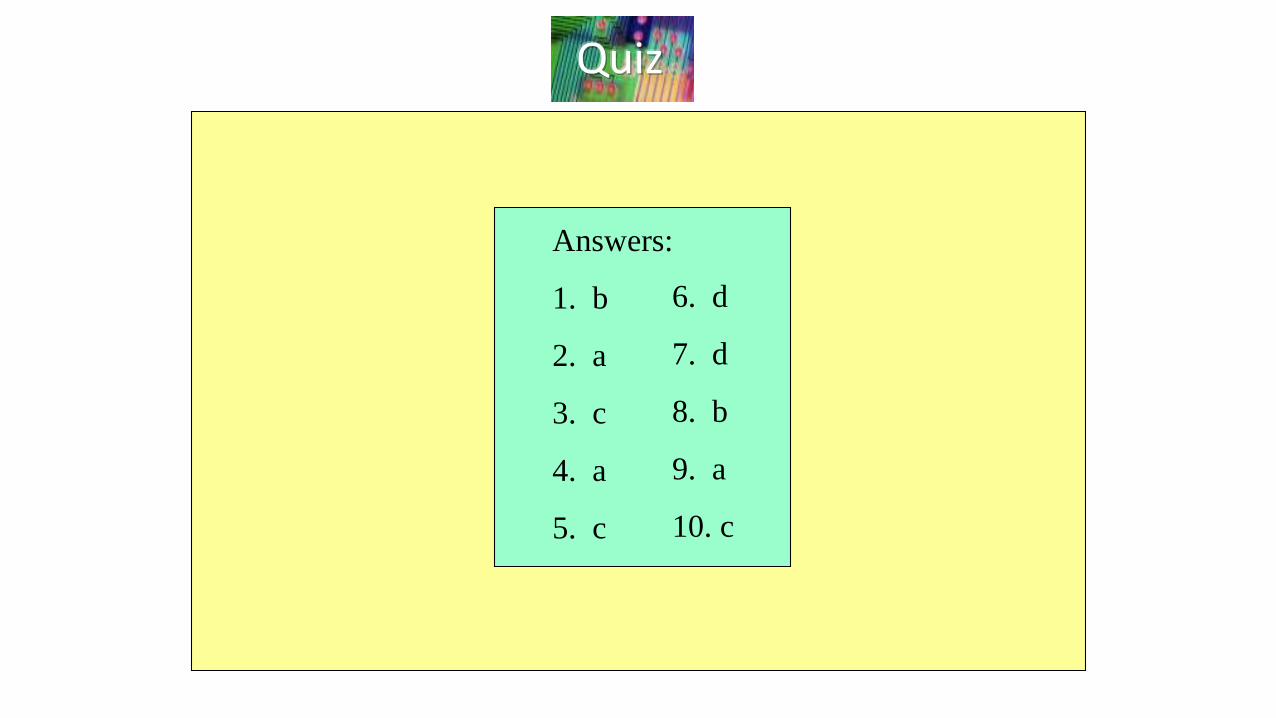
Answers:
1. b
2. a
3. c
4. a
5. c
6. d
7. d
8. b
9. a
10. c


![ch2[ M0RPHOLOGY]](https://img.pdfslide.tips/doc/110x75/577c828e1a28abe054b14569/ch2-m0rphology.jpg)