Embed Size (px)
Citation preview

BIFACIAL CELLS
EXISTING TECHNOLOGIES &
REQUIREMENTS
Y. Veschetti
Mail : [email protected] CEA/INES-RDI, 50 Av. Du Lac Léman, 73377 Le Bourget du Lac, FranceBIFI WORKSHOP
2ND EDITION
CELL SESSION

bifi PV workshop 2014.05.26 Chambéry
VESCHETTI Yannick
OUTLINE
TRENDS IN PV CELLS TECHNOLOGY
BIFACIAL CELL TECHNOLOGIES
- State of the art: lab & industrial scale
- Process characteristics
- Material sensitivity
REQUIREMENTS FOR BIFACIAL APPLICATION
CONCLUSION
2

bifi PV workshop 2014.05.26 Chambéry
VESCHETTI Yannick
Characteristics of the standard p-type industrial process
• Simple: Few fabrication steps, limited CAPEX• Most cell production lines are based on p-type standard technology• High experience from mass production• Continuous improvement in efficiency over the last years • Adapted to mono Cz and to mc-Si
3
A very competitive p-type process
p+ BSF & contact
ARC coating (SiN)
P-type substrate
N++ -emitter
Al contact
Wafer Eta (%)
mc-Si 17.5
Cz 19.0

bifi PV workshop 2014.05.26 Chambéry
VESCHETTI Yannick
P-TYPE PROCESS EVOLUTION
To keep improving the efficiency, the standard p-type technology will be more complex: --> end of Al-BSF
Development of PERC cell technology with additional process steps as:Al2O3, laser opening, advanced surface cleaning, …
Room for alternative technologies if cost/Wp remain competitive
International
Technology
Roadmap for
Photovoltaic
(ITRPV),
5th edition, March
2014, www.itrpv.net
4

bifi PV workshop 2014.05.26 Chambéry
VESCHETTI Yannick
Courtesy of CEA-INES
Bifacial technologiesPERT technology
Passivated Emitter Rear Totaly Diffused
Courtesy of Sanyo-PANASONIC
Heterojonction technology
5
IBC technologyInterdigitated Back Contact
Courtesy of ISC Konstanz

bifi PV workshop 2014.05.26 Chambéry
VESCHETTI Yannick
HIGH TEMPERATURE APPROACH : PERT *
• Mostly developed on n-type Cz Si
• Compatible with current production lines
• Efficiency improvement: From 18.5% in 2009 to
20.7% in 2014.
SiO2\SiN
Si(n)Phosphorous BSF
Boron Emitter
SiO2/SiN
Back grid
Front grid
PERT: Passivated Emitter Rear Totally diffused
6
PERT Voc (mV) Jsc
(mA/cm²)
FF (%) Eta (%)
N-type Cz 650.0 39.0 79.0 20.0
Current PERT cell parameters

bifi PV workshop 2014.05.26 Chambéry
VESCHETTI Yannick
PERT CELL: STATE OF THE ART
7- R. Kopecek & J. Libal, PV International, Sep 2013- Proceedings of SiliconPV & nPV workshop 2014, ‘Hertogenbosch |
Company/ institute Country Technology Metallization Status Efficiency Module
ECN Netherlands Diffused
Screen-printing Laboratory 20.0 +/- 0.5
ISC Germany Diffused CEA-INES France Diffused, Implanted
Suniva USA ImplantedIrysolar France DiffusedISFH Germany Diffused
Motech Taiwan DiffusedApplied Mat USA Implanted
Tetrasun USA Diffused? Copper-plating Pilot-line 20.5-21.0 Bifacial
Bosch-Solar Germany Hybrid/implanted Screen-printing Pilot-line 20.5 ?
bsolar Israel/Germany Implanted?Screen-printing
Production
19.0 Bifacial
YINGLI China Diffused 19.5 Monofacial
PVGS Japan Diffused 19.5-20 Bifacial
LG Electronics Korea Implanted 20.5 - 21 Monofacial
• More and more academic and industrial actors• Different process technology• All actors on n-type Si except bsolar• Efficiency potential towards 21% using screen-printing

bifi PV workshop 2014.05.26 Chambéry
VESCHETTI Yannick
PROCESS SPECIFICITY
BORON DIFFUSION:
• High temperature required for B-diffusion: 900°C-1050°C• Potential impact on bulk lifetime• Limited experience in production• Existing solutions : Gas diffusion: BBr3 (Tempress, CT), BCl3 (SEMCO) Solid-source: SOD or APCVD/PECVD doped layers Implantation (ion implantation/plasma immersion)
B-emitter passivation:
• Thermal oxidation (dry or wet)• Al2O3 (ALD/PECVD)• Chemical oxide (NAOS)
Contacts:
• Ag/Al on B doped layer• Ag on P doped layer• Sensitive co-firing
8

bifi PV workshop 2014.05.26 Chambéry
VESCHETTI Yannick
EFFICIENCY LIMITATION
B. Lim et al. | March 27, SiliconPV & nPV workshop 2014, ‘Hertogenbosch | 9
• Important gap between i-Voc (before metallization) and final cell Voc• Metal penetration into the diffused region and degrades the metal-Si
interface• B-emitter contact correspond to more than 40% of the entire cell J0.
A. Elder et al.Prog. Photovolt: Res. Appl. (2014)
9

bifi PV workshop 2014.05.26 Chambéry
VESCHETTI Yannick
IMPACT OF MATERIAL QUALITY
10
• Many studies showed thatefficiency remain stable overdifferent suppliers, ρ, positions• Eta: 19.9% - 20.4% fortaubulk: 500µs to 4ms
M. Forster, nPV workshop, Hertogenbosch 2014
• Process also compatiblefor alternatives materials- n-type Monolike Si: 19% [1]- mc-Si(n) EG: eta 16.2% [2]
Cz cells
Fraction available: 16% - 90%Average efficiency: 18.8%[1] Y. Veschetti et al. Proceedings PVSEC Paris, 2013
[2] T. Schutz-Kuchly et al. Prog. Photovolt: Res. Appl. 2013; 21:1214–1221
bifi PV workshop 2014.05.26 Chambéry
VESCHETTI Yannick
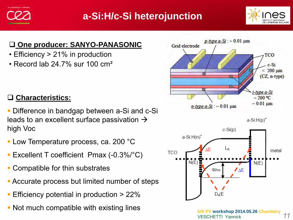
a-Si:H/c-Si heterojunction
One producer: SANYO-PANASONIC
• Efficiency > 21% in production• Record lab 24.7% sur 100 cm²
Source Sanyo Characteristics:
Difference in bandgap between a-Si and c-Si leads to an excellent surface passivation high Voc
Low Temperature process, ca. 200 °C
Excellent T coefficient Pmax (-0.3%/°C)
Compatible for thin substrates
Accurate process but limited number of steps
Efficiency potential in production > 22%
Not much compatible with existing lines11

HET CELL - STATE OF THE ART (R&D)
050
100150200250300350400450
USA+Canada
Europe
Japan
Rest of Asia
*Analyse from Scopus database
WR
21,5%
WR
23,7%
WR
20,1%WR
18,1%
WR
24,7%
Publications /year on « Silicon heterojunction solar cells »
• Japan leader in HET• Europe strong
expertise and many institutes involved
• Asia growing interest
12
Institute/company JSC (mA/cm²) VOC (mV) FF (%) Efficiency (%) area (cm²)
Panasonic 39.5 750 83.2 24.7 100Kaneka 40.0 738 81.9 24.2 171Choshu 37.3 733 81.8 22.3 240
R&R 38.1 734 79.9 22.3 240EPFL 39.1 728 78.6 22.4 4
CEA – INES 38.7 730 78.8 22.3 105AUO 37.5 724 81.9 22.3 240
P-J. Ribeyron et al. nPV workshop, Hertogenbosch 2014

STATE OF THE ART AT THE PILOT LINE/INDUSTRIAL LEVEL
• Several pilot lines running• BUT only one player at the
industrial level• Best cell efficiencies
reported > 22%• Mean efficiency ???
USA
KOREA
JAPAN900 MW
CHINAX pilot lines
EUROPE
• Difficulties to compete against mainstream technology • Hard times from 2011 due to PV crisis oversupply and price drop
• Since 2009: Growing interest at the industrial level
13

Higher sensitivity of the Wafer quality on the HET efficiency Voc is the leading parameter for HET
More than 1 % efficiency difference for the same cell process FlowStrong effect of Interstitial oxygen content and related defect distributionEffect of thermal donors to be adressed
IMPACT OF MATERIAL QUALITY
P-J. Ribeyron et al. nPV workshop, Hertogenbosch 2014
Results on INES
HET pilot line
14
bifi PV workshop 2014.05.26 Chambéry
VESCHETTI Yannick
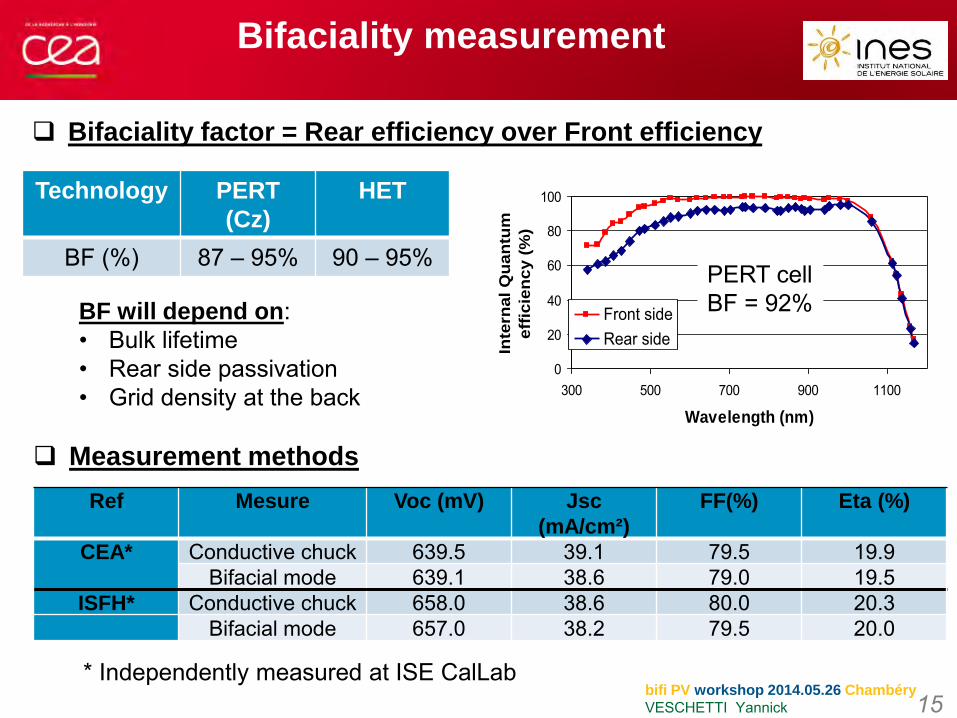
Bifaciality measurement
Bifaciality factor = Rear efficiency over Front efficiency
15
Technology PERT
(Cz)
HET
BF (%) 87 – 95% 90 – 95%
0
20
40
60
80
100
300 500 700 900 1100
Wavelength (nm)
Inte
rnal Q
uan
tum
eff
icie
ncy (
%)
Front sideRear side
BF will depend on:• Bulk lifetime• Rear side passivation• Grid density at the back
PERT cellBF = 92%
Ref Mesure Voc (mV) Jsc
(mA/cm²)
FF(%) Eta (%)
CEA* Conductive chuck 639.5 39.1 79.5 19.9Bifacial mode 639.1 38.6 79.0 19.5
ISFH* Conductive chuck 658.0 38.6 80.0 20.3Bifacial mode 657.0 38.2 79.5 20.0
* Independently measured at ISE CalLab
Measurement methods

bifi PV workshop 2014.05.26 Chambéry
VESCHETTI Yannick
REQUIREMENTS IN
BIFACIAL CONFIGURATION
No conductive/reflective chuck
Illumination at the front and at the back
Increase of current in the cell 5 (up to 15A for 6 ‘’ cell) Additional resistive losses The cell will not be optimized Need to consider Vbd
A I-V measurement system with
simultaneous front & back illumination
Is necessary
Alternative:
If back Jsc ≈ front Jsc Evaluate resistive losses with higher front illumination (1.5 Sun)
0 to 1000 W/m²
0 to x W/m²
16

CONCLUSION
17
Remaining challenges:
• Cell efficiency is not enough should be confirmed at module level• Cell processing cost should not be too far from std technology Process simplicity, low consumables, high efficiency, …• Process qualification is necessary (Stability, low illumination, Vbd, …)• Cost of n-type wafer (+15% versus p-type) and access to high quality Alternatives material: mc-Si /monolike Si• Need more data on cell performances in bifacial configuration
Two technologies well suited for bifacial application
More & more actors, starting of pilot-lines, production lines
Technology Front eta Process
simplicity
Material
compatibily
Line
compatibility
T° coef
PERT + - ++ + -HET ++ + - - +

Commissariat à l’énergie atomique et aux énergies alternativesINES RDI | Savoie Technolac – BP332 – 50 avenue du Lac Léman73377 Le Bourget-du-LacT. +33 (0)4 79 79 29 38 Email : [email protected]
Etablissement public à caractère industriel et commercial | RCS Paris B 775 685 019
Direction de la Recherche TechnologiqueLaboratoire d’innovation pour les technologies des énergies nouvelles et les nanomatériauxDépartement des Technologies SolairesLaboratoire des Matériaux et Procédé pour le Solaire
Thank You!