Embed Size (px)
Citation preview

Mand Labs presents
Diode

Types of materials
• Conductors: Metals
• Insulators: Non metals
• Semiconductors: Behavior between conductors and insulators

Semiconductor
• Electrical properties between that of conductor and insulator
• Examples: Silicon (Si), Germanium (Ge), Phosphorous (P), Gallium Arsenide (GaS), GaP (Gallium Phosphide)
• Few number of free electrons
• Electrons tightly packed in crystal lattice
Silicon Crystal

Pure Silicon
• Without Si, this would have been a Dark World
• Found in sand, 27.7% of earth crust
• Si Atom has 4 electrons in its outermost shell
• Si atoms share electrons and form crystal
• Pure Si is rare, Impure Si is dark grey in color
Silicon Atomic Structure

Si crystal

Cooking
• We are doping
• Doped Si has useful electrical properties
• Here, doping will create deficiency of electrons

Cooking Result : P-type Dish
Hole: Deficiency of Electron

N-type Dish
Silicon + Phosphorous

Doping
• Make semiconductors conducting in nature by adding impurities
• Impurities can either can either add free electrons or create deficiency of electrons
• Ideal for making electronic components
• Control the flow of current on your will
• Why not metals: They always conduct

Combine P-type and N-type
• P-Type and N-Type Silicon can conduct in both directions
• P-type contains free holes and N-type contains free electrons
• We combine P-type and N-type such that current can only flow from P to N

Diode
• A One way valve
• Door that opens up only in one direction
• To open up door, apply a minimum electrical force of 0.6-0.7 V in the right direction
• Right Direction of push: P to N
• Current passes the P-N Junction

P and N Identification
• Silver stripe represents N side
• Opposite to silver stripe (black portion) represents P side

Minimum Electrical Force
Electrons will flow from P to N if a forward force or voltage of 0.6 V is applied

Forward Biasing
• Positive terminal of battery repels holes and they cross the p-n junction
• Negative terminal of battery repels electrons and they cross the p-n junction

Precautions
Always use a resistor in series with diode
Chip may melt or crackCurrent flow in both directions
Current flow in wrong directionSudden current may zap diode
Never allow too much forward current through diode
Never allow too much reverse voltage across diode

Various types of diodes
Power Rectifier

Applications
• Mobile Chargers: AC to DC conversion; Rectification
• Detect radio signals, multiply voltage, perform logic
• Protection against voltage spikes
• Detect presence of light
• Voltage Regulation
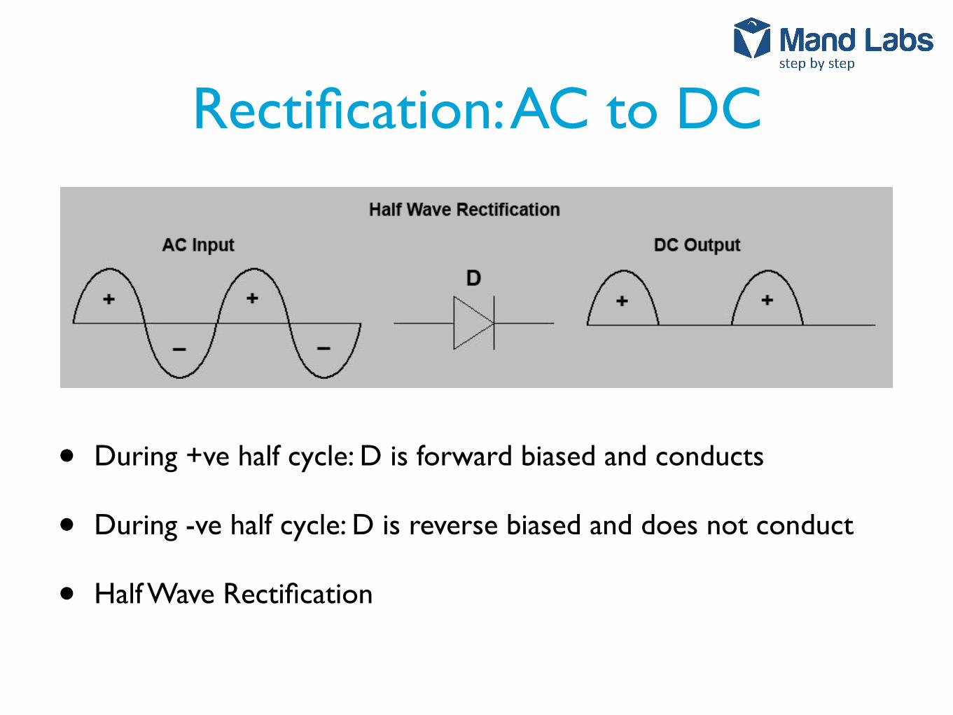
Rectification: AC to DC
• During +ve half cycle: D is forward biased and conducts
• During -ve half cycle: D is reverse biased and does not conduct
• Half Wave Rectification
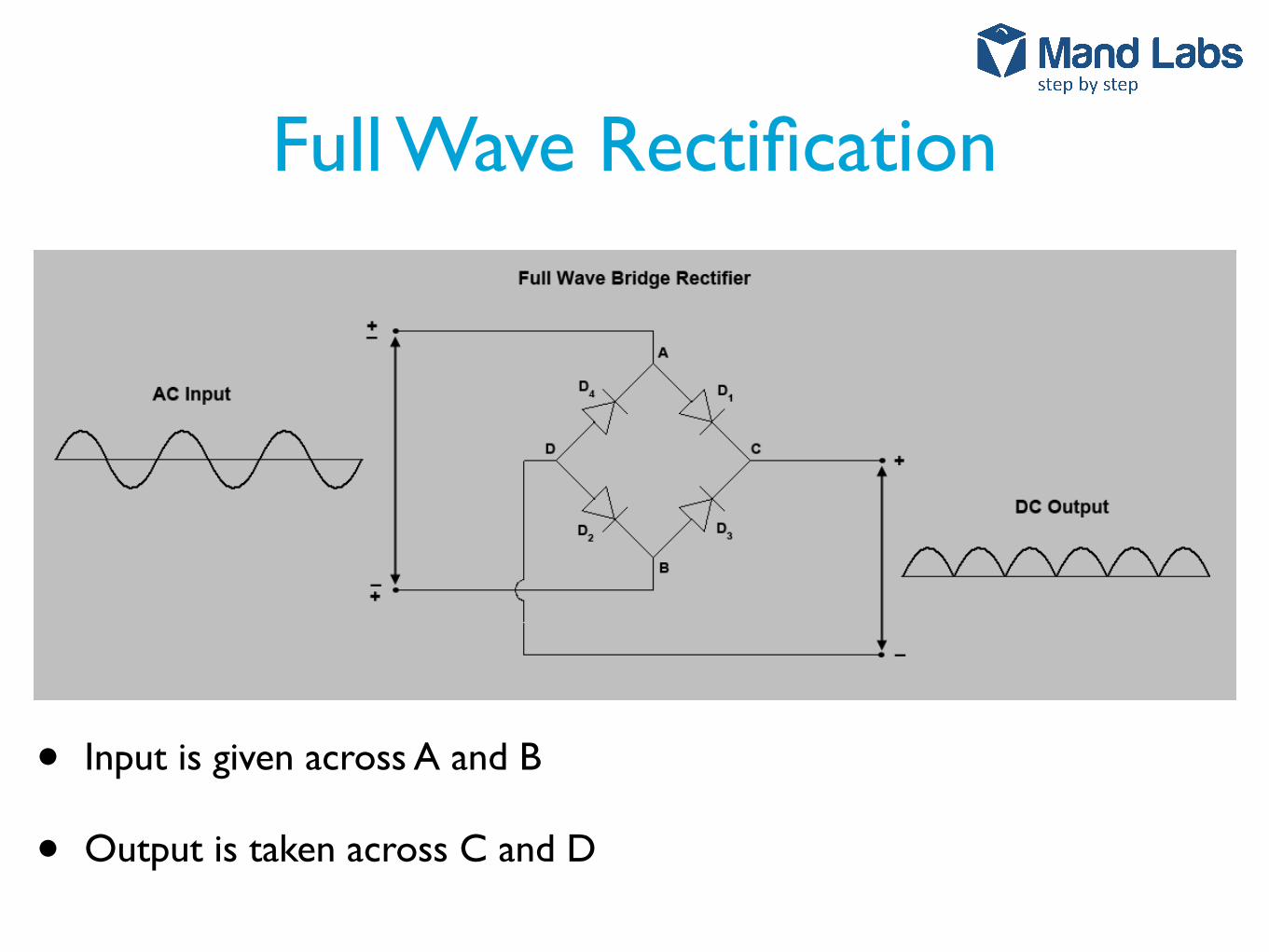
Full Wave Rectification
• Input is given across A and B
• Output is taken across C and D

Digital Logic Gates
Make Electronic Devices
Think, Analyze and Act
Building Blocks of Digital Devices

A Logic Gate
• Electronically Controlled Switch
• Provides output based on the inputs
• In digital: 2 kinds of input and output, 1 and 0
• 1 stands for high (any input voltage ≥ 3.5 Volts)
• 0 stands for low (any input voltage ≤ 1 Volts)
• There can be multiple inputs, but there is only output

NOT Gate
Input A Output Q1 00 1
Inverter: Inverts the inputInput OutputFail PassPass Fail
• You are writing history exam and there are only two outcomes- pass or fail
• We pass your result through an inverter

OR Gate
Input A Input B Output Q0 0 0
0 1 11 0 1
1 1 1
Either A or B or both
• You have to pass in any one of the subjects to get overall pass
• There can be multiple inputs
Q = A + B

AND Gate
Input A Input B Output Q0 0 0
0 1 01 0 0
1 1 1
• You have to pass in all the subjects to get overall pass
• There can be multiple inputs
Q = A.B

NOR Gate
Input A Input B Output Q0 0 1
0 1 01 0 0
1 1 0
OR Gate + NOT Gate
• You have to fail in all the subjects to get overall pass
• There can be multiple inputs
Q = (A + B)′
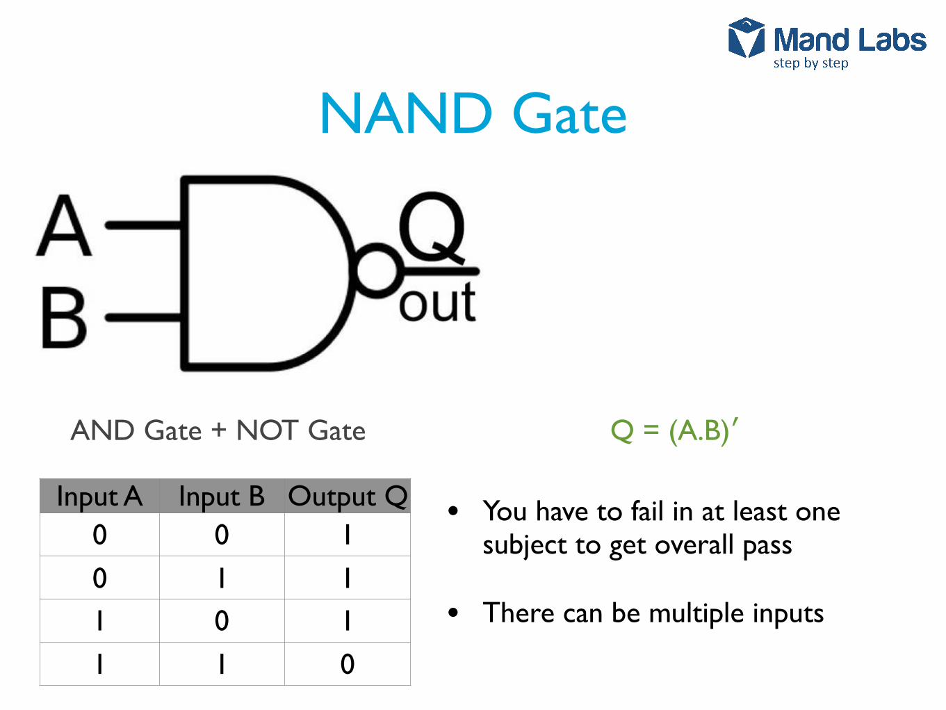
NAND Gate
Input A Input B Output Q0 0 1
0 1 11 0 1
1 1 0
AND Gate + NOT Gate
• You have to fail in at least one subject to get overall pass
• There can be multiple inputs
Q = (A.B)′

Credits
• Getting Started in Electronics by Forest M Mims (published by Radio Shack)