Embed Size (px)
Citation preview
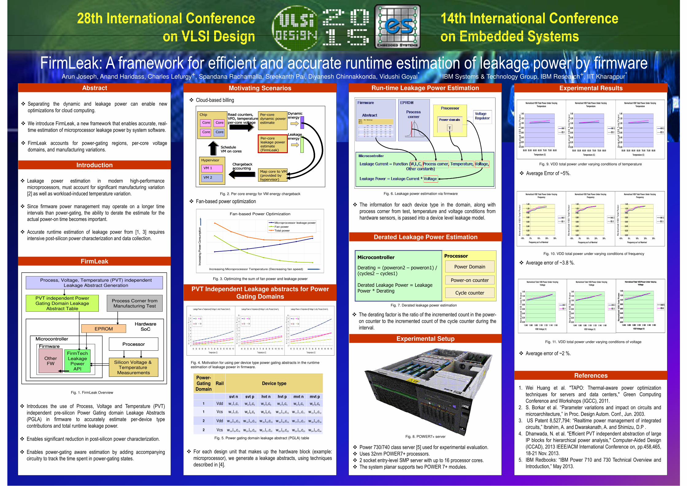
FirmLeak: A framework for efficient and accurate runtime estimation of leakage power by firmware
Abstract Run-time Leakage Power Estimation Experimental Results
FirmLeak
Introduction
References
PVT Independent Leakage abstracts for Power
Gating Domains
Arun Joseph, Anand Haridass, Charles Lefurgy+, Spandana Rachamalla, Sreekanth Pai, Diyanesh Chinnakkonda, Vidushi Goyal* IBM Systems & Technology Group, IBM Research+, IIT Kharagpur*
� Separating the dynamic and leakage power can enable new
optimizations for cloud computing.
� We introduce FirmLeak, a new framework that enables accurate, real-
time estimation of microprocessor leakage power by system software.
� FirmLeak accounts for power-gating regions, per-core voltage
domains, and manufacturing variations.
Normalized VDD Total Power Under Varying
Temperature
0.00
0.20
0.40
0.60
0.80
1.00
1.20
1.40
50.00 55.00 60.00 65.00 70.00 75.00 80.00
Temperature (C)
No
rma
liz
ed
VD
D T
ota
l P
ow
er
HW 3
ES 3
Normalized VDD Total Power Under Varying
Temperature
0.00
0.20
0.40
0.60
0.80
1.00
1.20
1.40
50.00 55.00 60.00 65.00 70.00 75.00 80.00
Temperature (C)
No
rma
liz
ed
VD
D T
ota
l P
ow
er
HW 1
ES 1
Normalized VDD Total Power Under Varying
Temperature
0.00
0.20
0.40
0.60
0.80
1.00
1.20
1.40
50.00 55.00 60.00 65.00 70.00 75.00 80.00
Temperature (C)
No
rma
liz
ed
VD
D T
ota
l P
ow
er
HW 2
ES 2
Normalized VDD Total Power Under Varying
Temperature
0.00
0.20
0.40
0.60
0.80
1.00
1.20
1.40
50.00 55.00 60.00 65.00 70.00 75.00 80.00
Temperature (C)
No
rma
liz
ed
VD
D T
ota
l P
ow
er
HW 3
ES 3
Normalized VDD Total Power Under Varying
Temperature
0.00
0.20
0.40
0.60
0.80
1.00
1.20
1.40
50.00 55.00 60.00 65.00 70.00 75.00 80.00
Temperature (C)
No
rma
liz
ed
VD
D T
ota
l P
ow
er
HW 1
ES 1
Normalized VDD Total Power Under Varying
Temperature
0.00
0.20
0.40
0.60
0.80
1.00
1.20
1.40
50.00 55.00 60.00 65.00 70.00 75.00 80.00
Temperature (C)
No
rma
liz
ed
VD
D T
ota
l P
ow
er
HW 2
ES 2
Normalized VDD Total Power Under Varying
Frequency
0.00
0.20
0.40
0.60
0.80
1.00
1.20
1.40
-10% 0% 10% 20% 30%
Frequency as % of Nominal
No
rma
liz
ed
VD
D T
ota
l P
ow
er
HW 3
ES 3
Normalized VDD Total Power Under Varying
Frequency
0.00
0.20
0.40
0.60
0.80
1.00
1.20
1.40
-10% 0% 10% 20% 30%
Frequency as % of Nominal
No
rma
liz
ed
VD
D T
ota
l P
ow
er
HW 1
ES 1
Normalized VDD Total Power Under Varying
Frequency
0.00
0.20
0.40
0.60
0.80
1.00
1.20
1.40
-10% 0% 10% 20% 30%
Frequency as % of Nominal
No
rma
liz
ed
VD
D T
ota
l P
ow
er
HW 2
ES 2
Normalized Total VDD Power Under Varying
Voltage
0.00
0.20
0.40
0.60
0.80
1.00
1.20
1.40
1.040 1.060 1.080 1.100 1.120 1.140 1.160
VDD Voltage (V)
No
rmali
zed
VD
D T
ota
l P
ow
er
HW 3
ES 3
Normalized Total VDD Power Under Varying
Voltage
0.00
0.20
0.40
0.60
0.80
1.00
1.20
1.40
1.040 1.060 1.080 1.100 1.120 1.140 1.160
VDD Voltage (V)
No
rma
liz
ed
VD
D T
ota
l P
ow
er
HW 1
ES 1
Normalized Total VDD Power Under Varying
Voltage
0.00
0.20
0.40
0.60
0.80
1.00
1.20
1.40
1.040 1.060 1.080 1.100 1.120 1.140 1.160
VDD Voltage (V)
No
rma
liz
ed
VD
D T
ota
l P
ow
er
HW 2
ES 2
Fig. 9. VDD total power under varying conditions of temperature
Fig. 10. VDD total power under varying conditions of frequency
Fig. 11. VDD total power under varying conditions of voltage
1. Wei Huang et al. "TAPO: Thermal-aware power optimization
techniques for servers and data centers," Green Computing
Conference and Workshops (IGCC), 2011.
2. S. Borkar et al. ‘‘Parameter variations and impact on circuits and
microarchitecture,’’ in Proc. Design Autom. Conf., Jun. 2003.
3. US Patent 8,527,794: “Realtime power management of integrated
circuits,” Ibrahim, A. and Dwarakanath, A. and Shimizu, D.P .
4. Dhanwada, N. et al. "Efficient PVT independent abstraction of large
IP blocks for hierarchical power analysis," Computer-Aided Design
(ICCAD), 2013 IEEE/ACM International Conference on, pp.458,465,
18-21 Nov. 2013.
5. IBM Redbooks: “IBM Power 710 and 730 Technical Overview and
Introduction,” May 2013.
� The information for each device type in the domain, along with
process corner from test, temperature and voltage conditions from
hardware sensors, is passed into a device level leakage model.
Fig. 6. Leakage power estimation via firmware
� Leakage power estimation in modern high-performance
microprocessors, must account for significant manufacturing variation
[2] as well as workload-induced temperature variation.
� Since firmware power management may operate on a longer time
intervals than power-gating, the ability to derate the estimate for the
actual power-on time becomes important.
� Accurate runtime estimation of leakage power from [1, 3] requires
intensive post-silicon power characterization and data collection.
Process, Voltage, Temperature (PVT) independent Leakage Abstract Generation
PVT independent Power Gating Domain Leakage
Abstract Table
Process Corner from Manufacturing Test
EPROMHardware
SoC
Microcontroller
FirmTechLeakagePower
API
Firmware
Other FW Silicon Voltage &
Temperature
Measurements
Processor
Motivating Scenarios
� Introduces the use of Process, Voltage and Temperature (PVT)
independent pre-silicon Power Gating domain Leakage Abstracts
(PGLA) in firmware to accurately estimate per-device type
contributions and total runtime leakage power.
� Enables significant reduction in post-silicon power characterization.
� Enables power-gating aware estimation by adding accompanying
circuitry to track the time spent in power-gating states.
� Cloud-based billing
Chip
Core Core
CoreCore
Per-coredynamic powerestimate
Per-coreleakage power
estimate(FirmLeak)
Read counters,VPD, temperature per-core voltage
Hypervisor
VM 1
VM 2
ScheduleVM on cores
Map core to VM(provided by hypervisor)
Dynamicenergy
Leakage energy
Chargeback
accounting
Chip
Core Core
CoreCore
Chip
Core Core
CoreCore
Per-coredynamic powerestimate
Per-coreleakage power
estimate(FirmLeak)
Read counters,VPD, temperature per-core voltage
Hypervisor
VM 1
VM 2
Hypervisor
VM 1
VM 2
ScheduleVM on cores
Map core to VM(provided by hypervisor)
Dynamicenergy
Leakage energy
Chargeback
accounting
Fig. 2. Per core energy for VM energy chargeback
� Fan-based power optimization
Fan-based Power Optimization
Increasing Microprocessor Temperature (Decreasing fan speed)
Incre
asin
g P
ow
er C
onsum
ption
Microprocessor leakage power
Fan power
Total power
Fig. 3. Optimizing the sum of fan power and leakage power
� For each design unit that makes up the hardware block (example:
microprocessor), we generate a leakage abstracts, using techniques
described in [4].
Power-
Gating
Domain
Rail Device type
svt n svt p hvt n hvt p mvt n mvt p
1 Vdd w1,l1,c1 w2,l2,c2 w3,l3,c3 w4,l4,c4 w5,l5,c5 w6,l6,c6
1 Vcs w7,l7,c7 w8,l8,c8 w9,l9,c9 w10,l10,c10 w11,l11,c11 w12,l12,c12
2 Vdd w13,l13,c13 w14,l14,c14 w15,l15,c15 w16,l16,c16 w17,l17,c17 w18,l18,c18
2 Vcs w19,l19,c19 w20,l20,c20 w21,l21,c21 w22,l22,c22 w23,l23,c23 w24,l24,c24
Fig. 5. Power gating domain leakage abstract (PGLA) table
� The derating factor is the ratio of the incremented count in the power-
on counter to the incremented count of the cycle counter during the
interval.
Derating = (poweron2 – poweron1) / (cycles2 – cycles1)
Derated Leakage Power = Leakage Power * Derating
Microcontroller Processor
Cycle counter
Power-on counter
Power DomainDerating = (poweron2 – poweron1) / (cycles2 – cycles1)
Derated Leakage Power = Leakage Power * Derating
Microcontroller Processor
Cycle counter
Power-on counter
Power Domain
Fig. 7. Derated leakage power estimation
Fig. 1. FirmLeak Overview
Leakage Power vs Temperature @ Voltage V1 volts, Process Corner S1
0
1
2
3
4
5
6
7
8
9
10
45 50 55 60 65 70 75 80 85 90 95 100 105 110
Temperature (C)
No
rma
lize
d L
ea
ka
ge
Po
we
r
D1 D2
D3 D4
Leakage Power vs Temperature @ Voltage V1 volts, Process Corner S2
0
1
2
3
4
5
6
7
8
9
10
45 50 55 60 65 70 75 80 85 90 95 100 105 110
Temperature (C)
No
rma
lize
d L
ea
ka
ge
Po
we
r
D1 D2
D3 D4
Leakage Power vs Temperature @ Voltage V1 volts, Process Corner S3
0
1
2
3
4
5
6
7
8
9
10
45 50 55 60 65 70 75 80 85 90 95 100 105 110
Temperature (C)
No
rma
lize
d L
ea
ka
ge
Po
we
r
D1 D2
D3 D4
Fig. 4. Motivation for using per device type power gating abstracts in the runtime
estimation of leakage power in firmware.
Derated Leakage Power Estimation
Experimental Setup
� Power 730/740 class server [5] used for experimental evaluation.
� Uses 32nm POWER7+ processors.
� 2 socket entry-level SMP server with up to 16 processor cores.
� The system planar supports two POWER 7+ modules.
Fig. 8. POWER7+ server
� Average Error of ~5%.
� Average error of ~3.8 %.
� Average error of ~2 %.