Embed Size (px)
Citation preview
卒 業 研 究 報 告
題 目
8ビットマイクロプロセッサの設計・製作
指 導 教 員
矢野 政顕 教授
報 告 者 学籍番号: 1050288 氏名: 山本 慎也
平成 17年 2月 22日
高知工科大学 電子・光システム工学科
i
目 次 第1章 はじめに …1 第2章 KUE-CHIP2 プロセッサ
2.1 KUE-CHIP2 とは …2 2.2 KUE-CHIP2 の構造 …2 2.3 KUE-CHIP2 の命令仕様 …3
2.3.1 アドレスモード …5 2.3.2 Shift・Rotate 命令の機能 …6
2.4 命令の実行フェーズ …8 2.5 KUE-CHIP2 の外部ピン仕様 …10
2.5.1 入力信号機能 …12 2.5.2 出力・双方向信号機能 …13
第3章 プロセッサの設計
3.1 KUE-CHIP2 設計 …14 3.2 クロックジェネレータ設計 …15 3.3 命令レジスタ・命令デコーダ設計 …16 3.4 コントローラ設計 …17 3.5 ALU・ACC・IX 設計 …23
3.5.1 ALU 設計 …24 3.5.2 ACC・IX 設計 …25 3.5.3 FLAG 設計 …26 3.5.4 8bit セル設計 …27
3.6 プログラムカウンタ・メモリアドレスレジスタ設計 …27 3.7 シンクロナイザ設計 …28 3.8 内部メモリ設計 …29 3.9 その他機能部の設計 …29
3.9.1 AB_SET 設計 …29 3.9.2 DBI_SET 設計 …30 3.9.3 OB_SET 設計 …31
第4章 動作検証と製作
4.1 シミュレーションおよび考察 …32 4.2 FPGA への書き込み …40 4.3 FPGA のピン配置 …40
ii
4.4 基板の設計 …41 4.4.1 ライブラリの設計 …41 4.4.2 基板の設計と実装 …43
第5章 まとめ …45 謝辞 …46 参考文献 …47 付録 1 1-1 プログラムのフローチャート …48 1-2 16 進数表示を 10 進数表示に変換するプログラム …49 付録 2 2-1 KUE_CHIP2.Vhd の記述 …51 2-2 CLOCKGEN の記述 …63 2-3 IR_IDC の記述 …65 2-4 CONTROL の記述 …68 2-5 ALU_ACC_IX の記述 …75 2-6 PC_MAR の記述 …89 2-7 SYNCRONIZER の記述 …91
2-8 IMEM の記述 …93 2-9 DBI_SET の記述 …95
2-10 OB_SET の記述 …96
1
第1章 はじめに 今日、LSI(Large Scale Integration)設計手法は急速に変化しており、設計の効率、設計期間の短縮、LSI の小型化や省電力化の点から回路図による設計からハードウェア記述言語HDL(Hardware Description Language)による設計に変化してきている。本研究の目的は、教育用 8 ビットマイクロプロセッサであるKUE-CHIP2(Kyoto University Education CHIP2)プロセッサのアセンブリ(Assembly)命令とアーキテクチャ(Architecture)を理解し VHDL(Very high speed integrated circuit HDL)を用いて KUE-CHIP2 と同じ機能を有する 8ビットマイクロプロセッサを設計することである。また、設計したプロセッサ
を FPGA(Field Programmable Gate Array)に実装し、KUE-CHIP2ボードに搭載して正しく設計されているかどうか確認する。KUE-CHIP2ボードへの搭載に際してはプリント基板 CADを用いてアダプタボードを設計・試作し、アダプタボード上に FPGAを実装する。 本論文は 5 章構成になっており、第 2 章と第 3 章では卒業研究で取り上げた
KUE-CHIP2 のアーキテクチャの概要と各マクロの設計について述べ、第 4 章で設計したプロセッサの動作検証とアダプタボードの設計・試作について述べ、
第 5章で本研究により得られた成果をまとめる。
2
第2章 KUE-CHIP2 プロセッサ
2.1 KUE-CHIP2 とは
KUE-CHIP2(Kyoto University Education CHIP2)とは大学などでの計算機教育のための教材として開発された 8 ビットのマイクロプロセッサである。内部のバスやレジスタ、内部制御信号の内容を KUE-CHIP2のボード上にある LEDおよび7セグメント表示用 LEDから観測することが出来ることと、ボード上にあるデータスイッチを用いて内部のレジスタやメモリに直接書き込み
が出来ることが特徴である。第 2 章では KUE-CHIP2 のアーキテクチャの概要について説明する[1][2]。
2.2 KUE-CHIP2 の構造
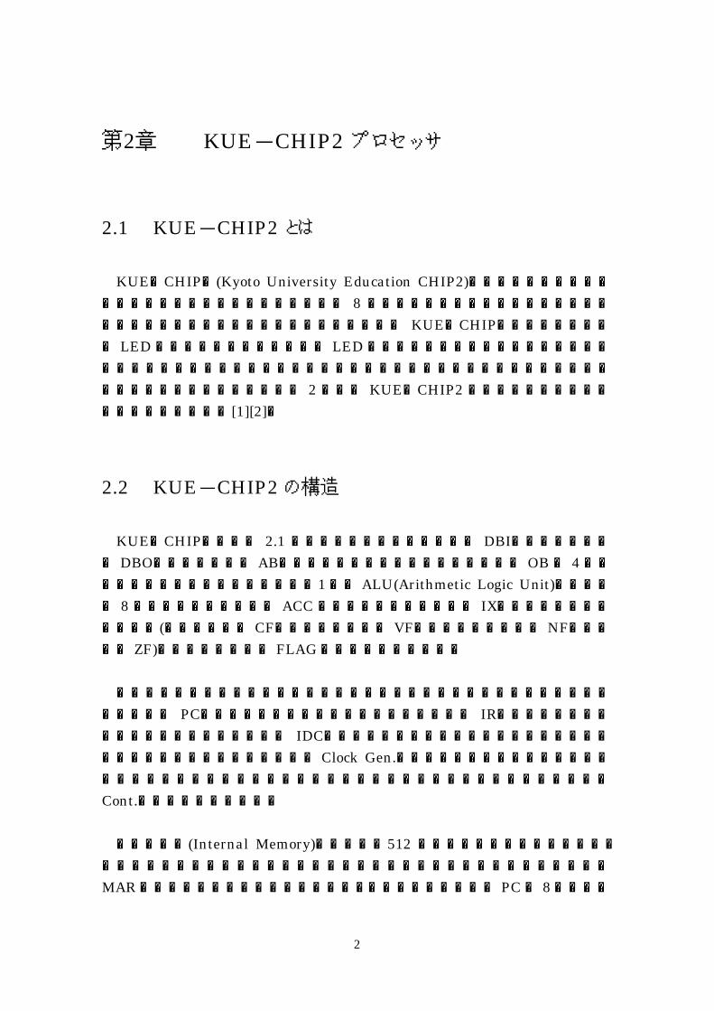
KUE-CHIP2は、図 2.1 に示すように入力データバス DBI、出力データバス DBO、アドレスバス AB、内部状態を観測するための観測バス OBの 4種類のバスを備えている。演算器は、1個の ALU(Arithmetic Logic Unit)、演算用の 8 ビットアキュムレータ ACC とインデックスレジスタ IX、演算結果に付随する情報(桁上げフラグ CF、桁あふれフラグ VF、ネガティブフラグ NF、零フラグ ZF)を設定するフラグ FLAGから構成されている。
制御部は、次に実行される命令のメモリ上でのアドレスを保持するプログラ
ムカウンタ PC、実行される命令を保持する命令レジスタ IR、命令レジスタの内容を解読する命令デコーダ IDC、外部から与えられるクロックからフェーズ信号を生成するクロック発生回路 Clock Gen.、クロック発生回路とともに順序回路を構成し、命令デコーダの出力をもとに各部に制御信号を送る制御回路
Cont.から構成されている。
内部メモリ(Internal Memory)としては、512 バイトのメモリを備えており、バイト単位で指定される。メモリアクセスの際にはメモリアドレスレジスタ
MARで保持したアドレスが用いられる。プログラムカウンタ PCが 8ビットで
3
あることから 0番地から 255番地はプログラム領域(program region)と呼ばれ、プログラムはこの範囲に書き込まなくてはならない。256 番地から 511 番地はデータ領域(data region)と呼ばれ、データを格納する領域として使用できる。
図 2.1 KUE-CHIP 2ブロックダイヤグラム
2.3 KUE-CHIP2 の命令仕様 マイクロプロセッサのアーキテクチャは大きく分けて RISC(Reduced
Instruction Set Computer)アーキテクチャと CISC( Complex Instruction Set Computer)アーキテクチャの2つに分かれる[3]。
KUE-CHIP2では CISCアーキテクチャを採用している。RISCアーキテクチャは1つの命令を単純にし、複数の命令を効率よく同時実行することで命令
処理能力を高めているのに対し、CISCアーキテクチャは、1つの命令で多くの処理が出来るように命令セットを高級言語に近づけ、複雑な処理を実行するこ
とで処理能力を向上させているのが特徴である。このために、CISCアーキテクチャを採用している KUE-CHIP 2の命令語は、表 2.1に示すように 1バイトあるいは 2バイトで構成されている。
FLAG ACC
IX ALU
SEL
IR
IDC
Syncro. Clock Gen.
Cont.
PC
SEL MAR
Inter.
MEM.
DBO
OB
DBI
AB
PANEL CLOCK
4
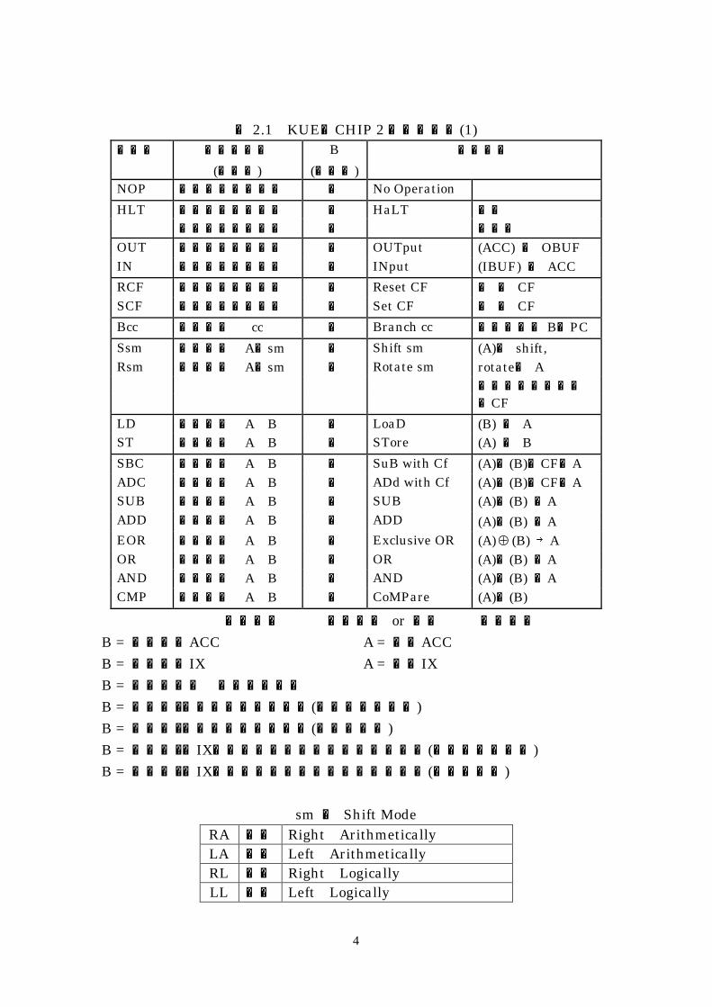
表 2.1 KUE-CHIP 2命令セット(1) 略記号 命令コード B 命令機能
(1語目) (2語目)
NOP 00000--- × No Operation 00001--- × 停止 HLT 0101---- ×
HaLT 未使用
OUT 00010--- × OUTput (ACC) → OBUF IN 00011--- × INput (IBUF) → ACC RCF 00100--- × Reset CF 0 → CF SCF 00101--- × Set CF 1 → CF Bcc 0011 cc ◎ Branch cc 条件成立で B→PC Ssm 0100 A0sm × Shift sm (A)→ shift, Rsm 0100 A1sm × Rotate sm rotate→ A はみ出したビット
→CF LD 0110 A B ○ LoaD (B) → A ST 0111 A B ◎ STore (A) → B SBC 1000 A B ○ SuB with Cf (A)-(B)-CF→A ADC 1001 A B ○ ADd with Cf (A)+(B)+CF→A SUB 1010 A B ○ SUB (A)-(B) →A ADD 1011 A B ○ ADD (A)+(B) →A
EOR 1100 A B ○ Exclusive OR (A) (B) →A OR 1101 A B ○ OR (A)∨(B) →A AND 1110 A B ○ AND (A)∧(B) →A CMP 1111 A B ○ CoMPare (A)-(B)
◎:必要 ○:必要 or 不要 ×:不要 B = 000:ACC A = 0:ACC B = 001:IX A = 1:IX B = 01-:d 即値アドレス B = 100:[d]絶対アドレス(プログラム領域) B = 101:(d)絶対アドレス(データ領域) B = 110:[IX+d]インデックス修飾アドレス(プログラム領域) B = 111:(IX+d)インデックス修飾アドレス(データ領域)
sm : Shift Mode
RA 00 Right Arithmetically LA 01 Left Arithmetically RL 10 Right Logically LL 11 Left Logically
5
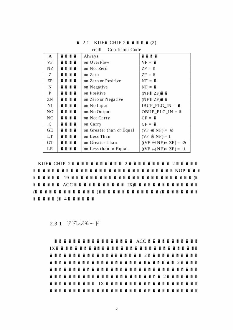
表 2.1 KUE-CHIP 2命令セット(2) cc : Condition Code
A 0000 Always 常に成立
VF 1000 on OverFlow VF = 1 NZ 0001 on Not Zero ZF = 0 Z 1001 on Zero ZF = 1
ZP 0010 on Zero or Positive NF = 0 N 1010 on Negative NF = 1 P 0011 on Positive (NF∨ZF)=0
ZN 1011 on Zero or Negative (NF∨ZF)=1 NI 0100 on No Input IBUF_FLG_IN = 0 NO 1100 on No Output OBUF_FLG_IN = 1 NC 0101 on Not Carry CF = 0 C 1101 on Carry CF = 1
GE 0110 on Greater than or Equal (VF NF) = 0
LT 1110 on Less Than (VF NF) = 1
GT 0111 on Greater Than ((VF NF)∨ZF) = 0
LE 1111 on Less than or Equal ((VF NF)∨ZF) = 1
KUE-CHIP 2の命令は、入出力命令が 2種類、シフト命令が 2種類、算術論理演算命令が8種類、ロード命令、ストア命令、ブランチ命令、NOP 命令、停止命令の全 19 種類から構成されている。アドレスの指定には、レジスタ(アキュムレータ ACCとインデックスレジスタ IX)と即値アドレス、絶対アドレス(プログラム領域とデータ領域)、インデックス修飾アドレス(プログラム領域とデータ領域)の 4種類がある。
2.3.1 アドレスモード
アドレスの指定のうちアキュムレータ ACC とインデックスレジスタ
IXを指定した場合は、各レジスタに格納されているデータを用いる。即値アドレスを指定した場合は、命令コードの 2語目をそのままデータとして用いる。絶対アドレスを指定した場合は、命令コードの 2語目を実効アドレスとし、実効アドレスに格納されているデータを用いる。イン
デックス修飾アドレスを指定した場合は命令コードの 2語目のデータとインデックスレジスタ IX に格納されているデータと加算を行った値を実効アドレスとして用い、実効アドレスに格納されているデータを用い
6
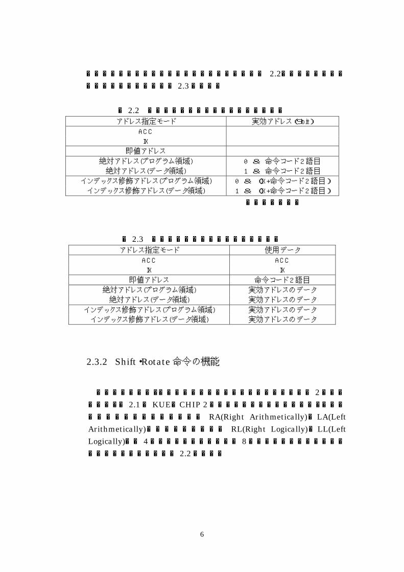
る。各アドレスモードにおける実効アドレスを表 2.2、アドレスモードにおける使用データを表 2.3に示す。
表 2.2 アドレスモードにおける実効アドレス アドレス指定モード 実効アドレス(9bit)
ACC
IX
即値アドレス
絶対アドレス(プログラム領域) 0 & 命令コード 2 語目
絶対アドレス(データ領域) 1 & 命令コード 2 語目
インデックス修飾アドレス(プログラム領域) 0 & (IX+命令コード 2 語目)
インデックス修飾アドレス(データ領域) 1 & (IX+命令コード 2 語目)
&は結合を表す
表 2.3 アドレスモードにおける使用データ アドレス指定モード 使用データ
ACC ACC
IX IX
即値アドレス 命令コード 2 語目
絶対アドレス(プログラム領域) 実効アドレスのデータ
絶対アドレス(データ領域) 実効アドレスのデータ
インデックス修飾アドレス(プログラム領域) 実効アドレスのデータ
インデックス修飾アドレス(データ領域) 実効アドレスのデータ
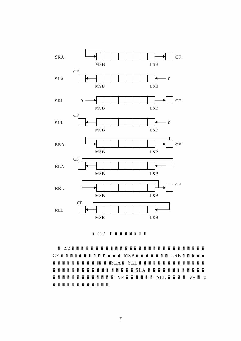
2.3.2 Shift・Rotate 命令の機能
シフト命令には、大きく分けて通常のシフトと巡回シフトの 2種類があるが、表 2.1の KUE-CHIP 2命令セットから分かるように、シフトモードには左右の算術シフト RA(Right Arithmetically)、LA(Left Arithmetically)、左右の論理シフト RL(Right Logically)、LL(Left Logically)の計 4種類があるため、全部で 8種類のシフト命令がある。各シフト命令の機能を図 2.2に示す。
7
図 2.2 シフト命令の機能
図 2.2から各シフト命令によって、はみ出したビットが桁上げフラグ
CFとなり、それは最上位ビットMSBか最下位ビット LSBのいずれかであることが分かる。また、SLAと SLLは動作が同じように見えるが、命令実行後のフラグの状態が異なり、SLA は実行後にオーバーフローが発生すれば桁あふれフラグ VF が変化するが SLL では常に VF は 0であるという違いがある。
SRA CF
SLA CF
SRL CF
SLL CF
RRA CF
RLA CF
RRL
RLL
MSB LSB
0
0
0
MSB LSB
MSB LSB
MSB LSB
CF
MSB LSB
MSB LSB
MSB LSB
MSB LSB
CF
8
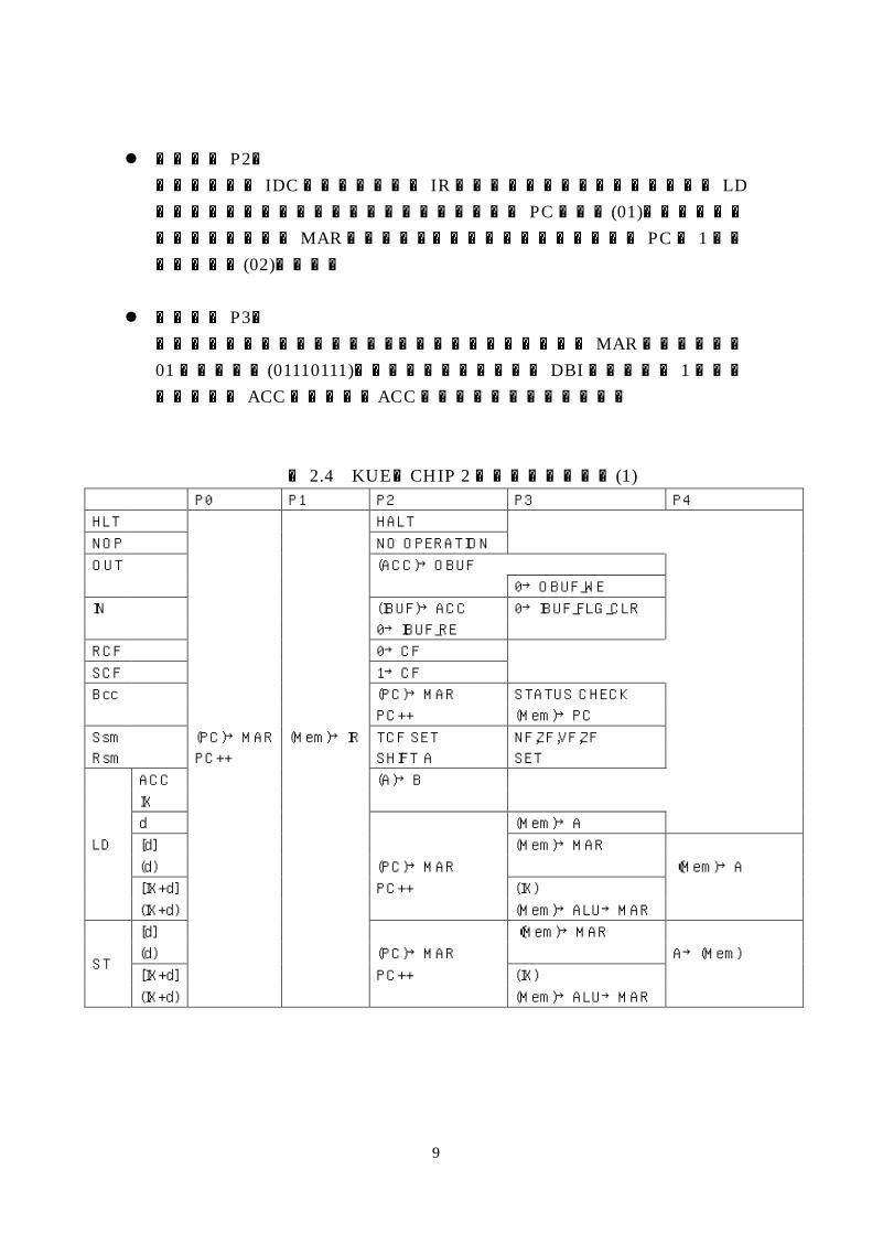
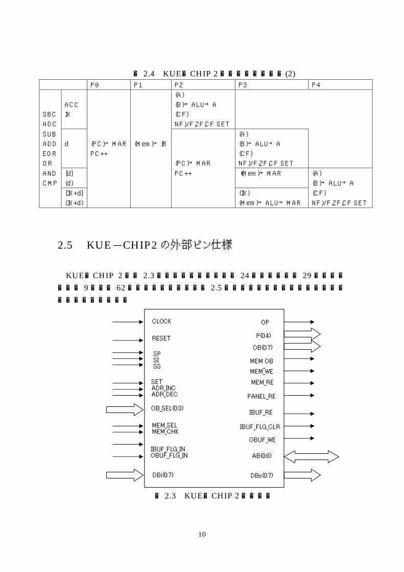
2.4 命令の実行フェーズ
KUE-CHIP 2は、前節(2.3節)で述べたように CISCアーキテクチャを採用しているので RISC アーキテクチャと異なり、命令を同時に行うことは出来ない。また、各命令を実行するのに必要な時間(フェーズ)も異なっており、最大で5 フェーズ(P0 から P4)で1つの命令を実行するようになっている。KUE-CHIP 2には、通常の動作モードである SS(Start / Stop)モードのほかに、1命令ごとに動作をとめる SI(Single Instruction)モードと1フェーズごとに動作をとめる SP(Single Phase)モードがある。これらのモードを利用して、各フェーズでどのように回路が動いているかが理解出来るようになっている。
フェーズ P0では、命令をフェッチするためにプログラムカウンタ PCに保持されているアドレスをメモリアドレスレジスタMARへ送る。この間にプログラムカウンタ PCは自動的に1増加する。
フェーズ P1 では、メモリに対して READ 動作が指示されメモリアドレスレジスタMARの内容を番地とするメモリのデータが、データバス DBIを通じて命令レジスタ IRへ送られてくる。送られてきたデータが命令レジスタ IRから命令デコーダ IDCへ移ることで命令を解読できるようになる。 以上の動作はどの命令でも共通であるが、フェーズ P2以降は命令によって異なる。KUE-CHIP 2の命令実行フェーズを表 2.4に示す。また、例としてプログラムカウンタ PCは 00番地を指していて、00番地に即値アドレスの LD命令(01100010)、01番地に(01110111)が格納されており、ACCに 01番地のデータをロードさせる命令の実行フェーズを次に示す。
フェーズ P0: プログラムカウンタ PCの内容をメモリアドレスレジスタMARに送り プログラムカウンタ PCを 1増加(01)する。
フェーズ P1: メモリアドレスレジスタMARの内容(00番地)をメモリに送り、データ (01100010)を入力バス DBIを通じて命令レジスタ IRへ送る。
9
フェーズ P2: 命令デコーダ IDCで命令レジスタ IRの内容を解読し、即値アドレスの LD命令であることが分かる。プログラムカウンタ PCの内容(01)を再びメモリアドレスレジスタMARに送られ、同時にプログラムカウンタ PCは 1増加されて内容(02)となる。
フェーズ P3: メモリの読み出しが行われる。メモリアドレスレジスタMARで指定された01番地の内容(01110111)が、読み出され入力バス DBIを通して第 1オペランドである ACCへ送られ、ACCはそのデータを保持する。
表 2.4 KUE-CHIP 2命令実行フェーズ(1) P0 P1 P2 P3 P4
HLT HALT
NOP NO OPERATION
OUT (ACC)→OBUF
0→OBUF_WE
IN (IBUF)→ACC 0→IBUF_FLG_CLR
0→IBUF_RE
RCF 0→CF
SCF 1→CF
Bcc (PC)→MAR STATUS CHECK
PC++ (Mem)→PC
Ssm (PC)→MAR (Mem)→IR TCF SET NF,ZF,VF,ZF
Rsm PC++ SHIFT A SET
ACC (A)→B
IX
d (Mem)→A
[d] (Mem)→MAR
(d) (PC)→MAR (Mem)→A
[IX+d] PC++ (IX)
LD
(IX+d) (Mem)→ALU→MAR
[d] (Mem)→MAR
(d) (PC)→MAR A→(Mem)
[IX+d] PC++ (IX) ST
(IX+d) (Mem)→ALU→MAR
10
表 2.4 KUE-CHIP 2命令実行フェーズ(2) P0 P1 P2 P3 P4
(A)
ACC (B)→ALU→A
SBC IX (CF)
ADC NF,VF,ZF,CF SET
SUB (A)
ADD d (PC)→MAR (Mem)→IR (B)→ALU→A
EOR PC++ (CF)
OR (PC)→MAR NF,VF,ZF,CF SET
AND [d] PC++ (Mem)→MAR (A)
CMP (d) (B)→ALU→A
[IX+d] (IX) (CF)
(IX+d) (Mem)→ALU→MAR NF,VF,ZF,CF SET
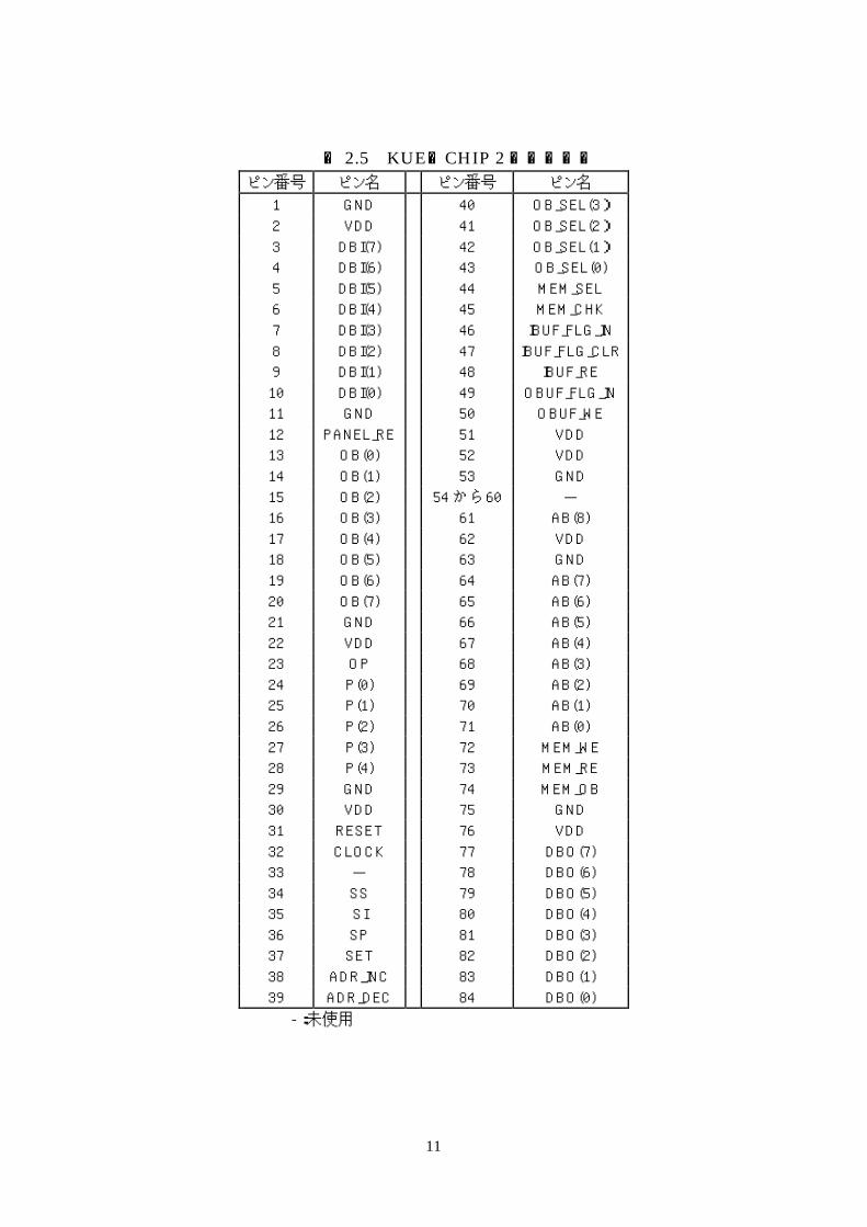
2.5 KUE-CHIP2 の外部ピン仕様
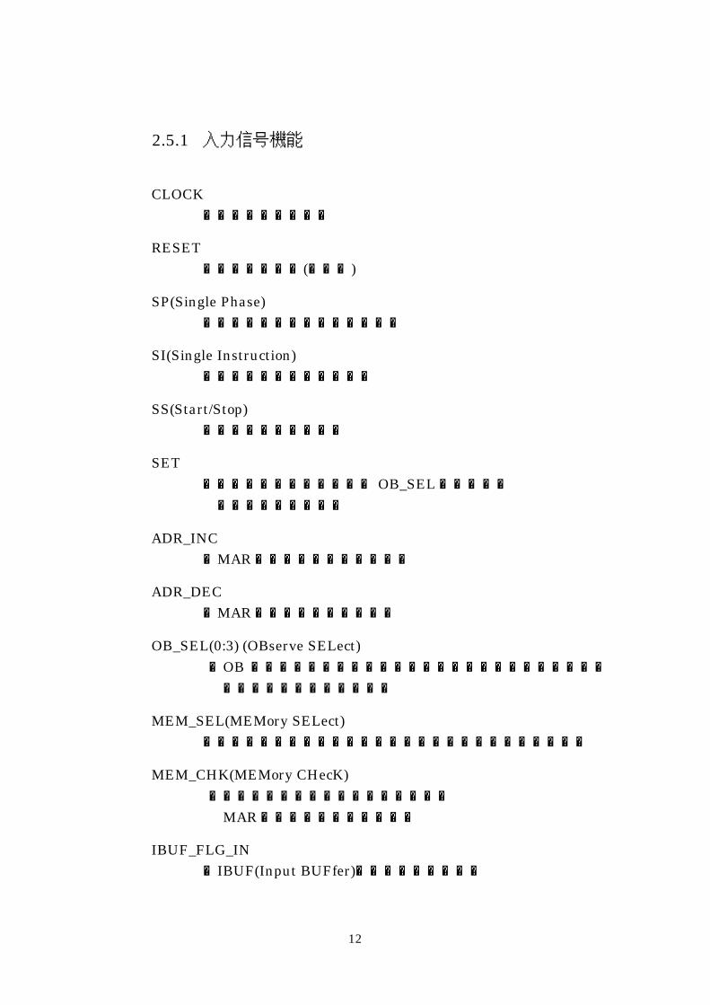
KUE-CHIP 2は図 2.3に示すように入力ピン 24本、出力ピン 29本、双方向ピン 9本、計 62ピンを備えている。表 2.5にピン配置を示すとともに各ピンの機能を説明する。
図 2.3 KUE-CHIP 2外部ピン
11
表 2.5 KUE-CHIP 2のピン配置 ピン番号 ピン名 ピン番号 ピン名
1 GND 40 OB_SEL(3)
2 VDD 41 OB_SEL(2)
3 DBI(7) 42 OB_SEL(1)
4 DBI(6) 43 OB_SEL(0)
5 DBI(5) 44 MEM_SEL
6 DBI(4) 45 MEM_CHK
7 DBI(3) 46 IBUF_FLG_IN
8 DBI(2) 47 IBUF_FLG_CLR
9 DBI(1) 48 IBUF_RE
10 DBI(0) 49 OBUF_FLG_IN
11 GND 50 OBUF_WE
12 PANEL_RE 51 VDD
13 OB(0) 52 VDD
14 OB(1) 53 GND
15 OB(2) 54 から 60 -
16 OB(3) 61 AB(8)
17 OB(4) 62 VDD
18 OB(5) 63 GND
19 OB(6) 64 AB(7)
20 OB(7) 65 AB(6)
21 GND 66 AB(5)
22 VDD 67 AB(4)
23 OP 68 AB(3)
24 P(0) 69 AB(2)
25 P(1) 70 AB(1)
26 P(2) 71 AB(0)
27 P(3) 72 MEM_WE
28 P(4) 73 MEM_RE
29 GND 74 MEM_OB
30 VDD 75 GND
31 RESET 76 VDD
32 CLOCK 77 DBO(7)
33 - 78 DBO(6)
34 SS 79 DBO(5)
35 SI 80 DBO(4)
36 SP 81 DBO(3)
37 SET 82 DBO(2)
38 ADR_INC 83 DBO(1)
39 ADR_DEC 84 DBO(0)
-:未使用
12
2.5.1 入力信号機能
CLOCK
:マスタークロック
RESET :リセット信号(非同期)
SP(Single Phase) :1フェーズだけ実行して停止
SI(Single Instruction) :1命令だけ実行して停止
SS(Start/Stop) :スタート/ストップ
SET :データスイッチの内容を OB_SELで指定した 記憶素子へ書き込む
ADR_INC :MARの値を1インクリメント
ADR_DEC :MARの値を1デクリメント
OB_SEL(0:3) (OBserve SELect) :OB を通じて観察する内部制御線、またはデータの書き込みを行う記憶素子を選択する
MEM_SEL(MEMory SELect) :内部メモリと外部メモリのどちらを使用するかを選択する
MEM_CHK(MEMory CHecK) :アドレスバスを外部から入力するか
MARが与えるのかを選択する
IBUF_FLG_IN :IBUF(Input BUFfer)のフラグを読み込む
13
OBUF_FLG_IN :OBUF(Output BUFfer)のフラグを読み込む
DBI(0:7) (Data Bus for Input) :入力データバス
2.5.2 出力・双方向信号機能
OP(OPeration)
:CPU(Central Processing Unit)が動作中か停止中かを示す
P(0:4) (Phase) :CPUが動作、停止している状態でのクロックフェーズを示す
OB(0:7) (OBserver bus) :観測用のバス
MEM_OB(external MEMory_OBserve enable) :外部メモリのデータを OBへ出力させるための信号
MEM_WE(external MEMory_Write Enable) :DBOのデータを外部メモリに書き込むための信号
MEM_RE(external MEMory_Read Enable) :外部メモリのデータを DBIに出力させるための信号
PANEL_RE(PANEL switch_Read Enable) :データスイッチの内容を DBIへ出力させるための信号
IBUF_RE(IBUF_Read Enable) :入力バッファのデータを DBIへ出力させるための信号
OBUF_WE(OBUF_Write Enable) :DBOのデータを出力バッファに書き込むための信号
DBO(0:7) (Data Bus for Output) :出力データバス
AB(0:8) (Address Bus) :双方向のアドレスバス。
MEM_CHKに従ってアドレスを入出力させる
14
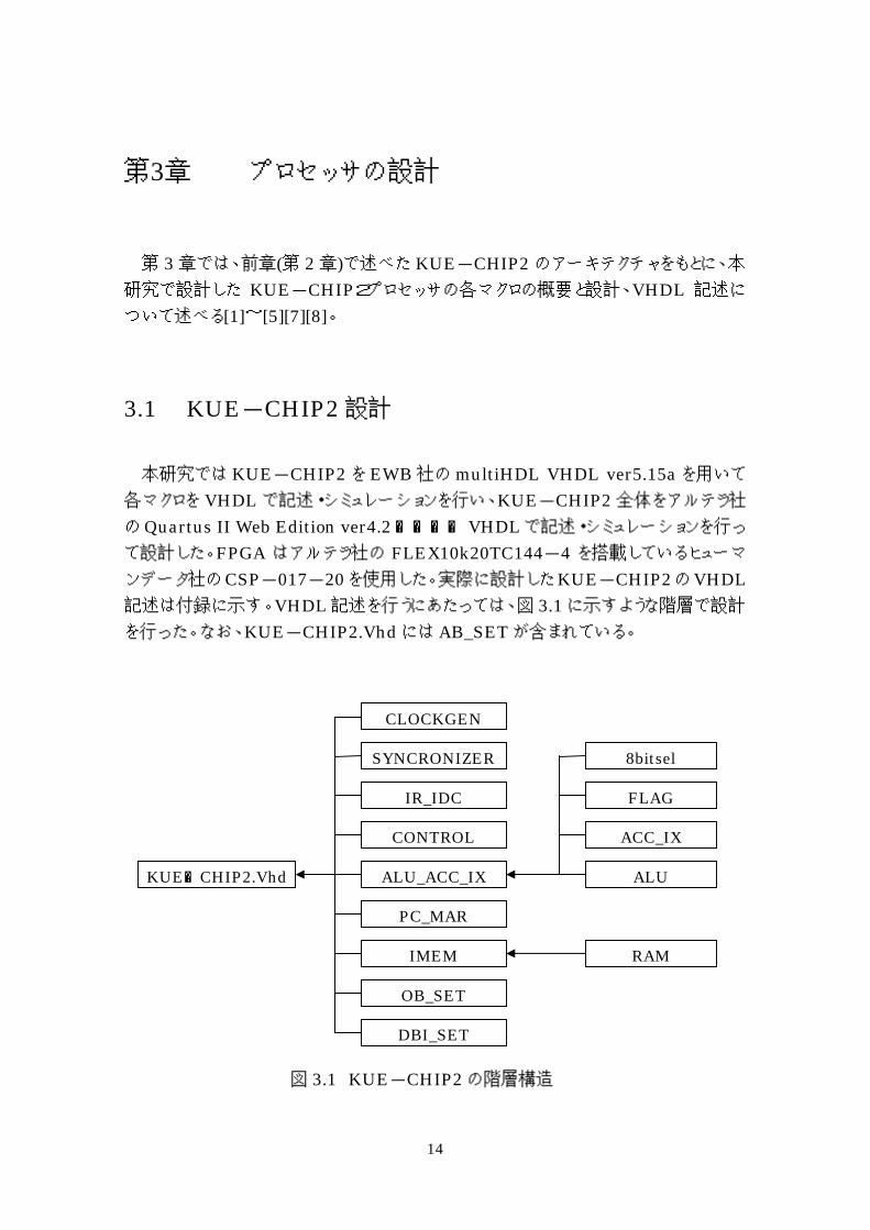
第3章 プロセッサの設計
第 3 章では、前章(第 2 章)で述べた KUE-CHIP2 のアーキテクチャをもとに、本
研究で設計した KUE-CHIP2プロセッサの各マクロの概要と設計、VHDL 記述に
ついて述べる[1]~[5][7][8]。
3.1 KUE-CHIP2 設計
本研究では KUE-CHIP2 を EWB 社の multiHDL VHDL ver5.15a を用いて
各マクロを VHDL で記述・シミュレーションを行い、KUE-CHIP2 全体をアルテラ社
の Quartus II Web Edition ver4.2を用いてVHDL で記述・シミュレーションを行っ
て設計した。FPGA はアルテラ社の FLEX10k20TC144-4 を搭載しているヒューマ
ンデータ社の CSP-017-20 を使用した。実際に設計した KUE-CHIP2 の VHDL記述は付録に示す。VHDL 記述を行うにあたっては、図 3.1 に示すような階層で設計
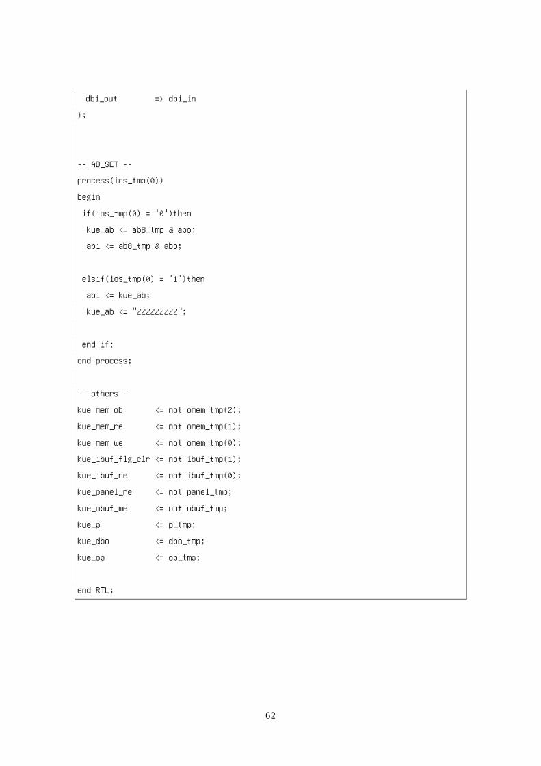
を行った。なお、KUE-CHIP2.Vhd には AB_SET が含まれている。
図 3.1 KUE-CHIP2 の階層構造
KUE-CHIP2.Vhd
CLOCKGEN
SYNCRONIZER
IR_IDC
CONTROL
ALU_ACC_IX
PC_MAR
IMEM
OB_SET
DBI_SET
ALU
ACC_IX
FLAG
8bitsel
RAM
15
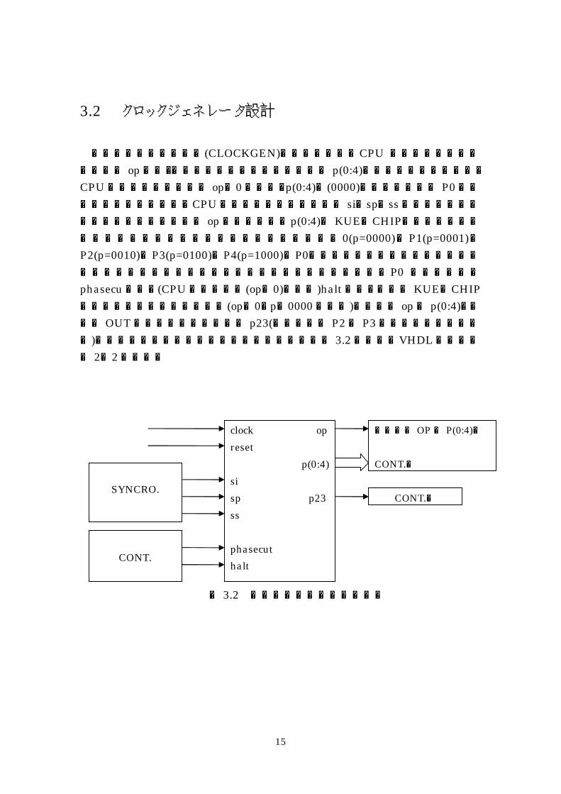
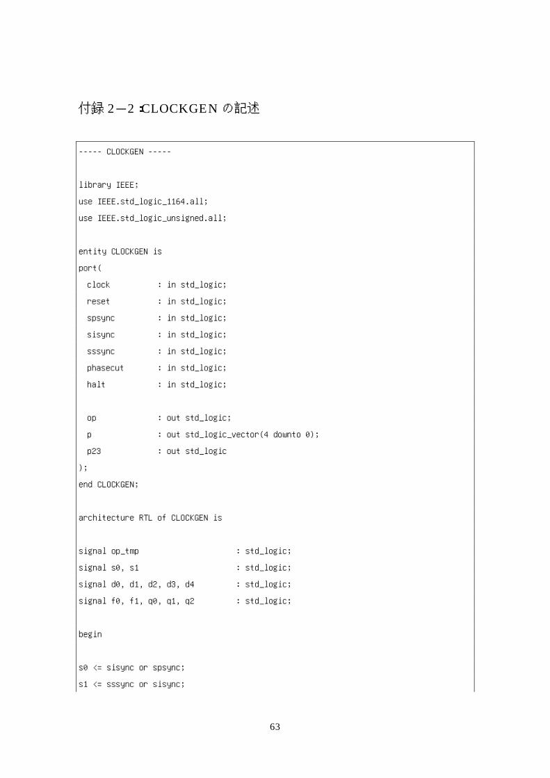
3.2 クロックジェネレータ設計 クロックジェネレータ(CLOCKGEN)の主な働きは、CPU が動作中か停止中
かを示す op信号、現在のクロックフェーズを示す p(0:4)を出力することである。CPUが停止状態のときは op=0を示し、p(0:4)は(0000)つまりフェーズ P0の状態であることを示す。CPUを動作させる命令である si・sp・ss信号がシンクロナイザから入力されると opは1を示し、p(0:4)は KUE-CHIP2ボードからのクロック信号が入力されるたびにフェーズをP0(p=0000)→P1(p=0001)→P2(p=0010)→P3(p=0100)→P4(p=1000)→P0→…と変化する。そして、コントローラより発せられる各命令によって決まるフェーズを、P0 の状態に戻すphasecu信号、(CPUを停止状態(op=0)にする)halt信号、または KUE-CHIP2ボードからのリセット信号(op=0、p=0000にする)をもとに opと p(0:4)、そして OUT命令の際に使用される p23(フェーズが P2か P3状態であることを示す)を出力する。クロックジェネレータの概要を図 3.2に示す。VHDL記述を付録 2-2に示す。
図 3.2 クロックジェネレータ概要
clock op reset p(0:4) si sp p23 ss phasecut halt
CONT.
SYNCRO.
本体出力 OPと P(0:4)へ CONT.へ
CONT.へ
16
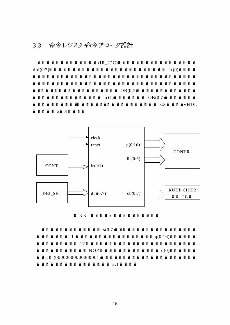
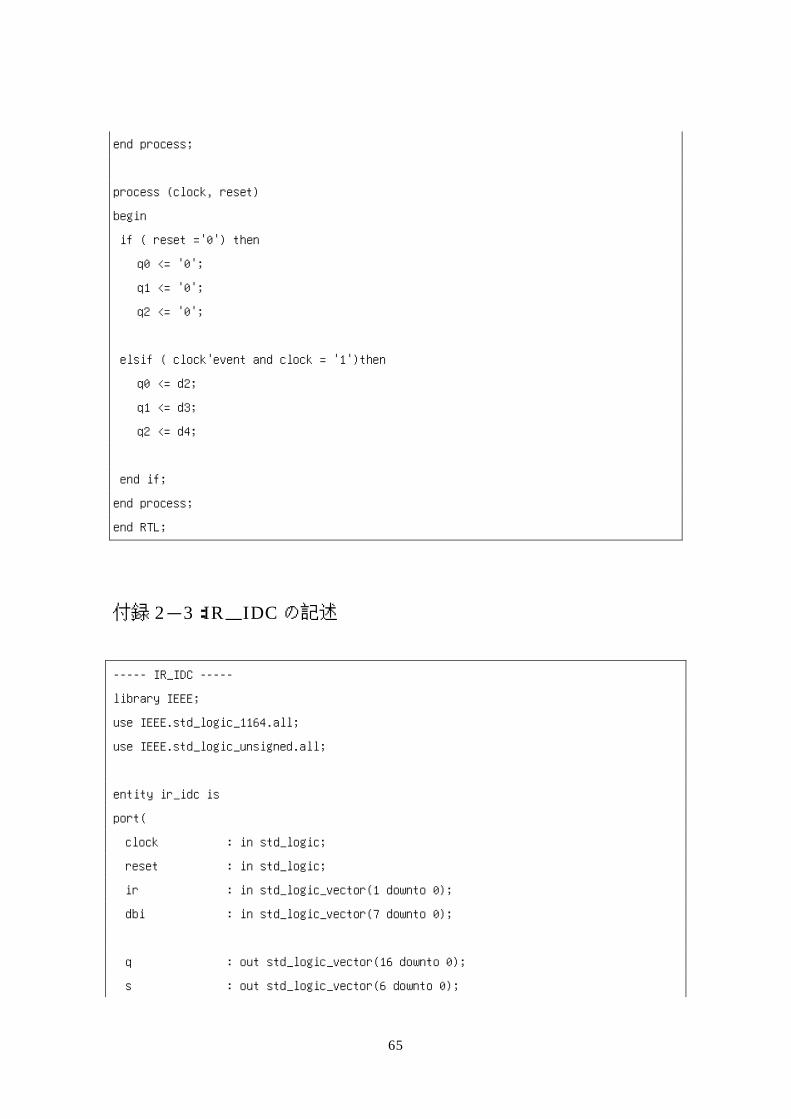
3.3 命令レジスタ・命令デコーダ設計 命令レジスタと命令デコーダ(IR_IDC)の動作は、命令レジスタでデータバス
dbi(0:7)を通過してきた命令データをコントローラから来た信号 ir(0)をもとに命令レジスタに保持するかしないかを判断し、保持する場合は命令デコーダで
データの解読を行い、どのような命令であるかをコントローラに送ることであ
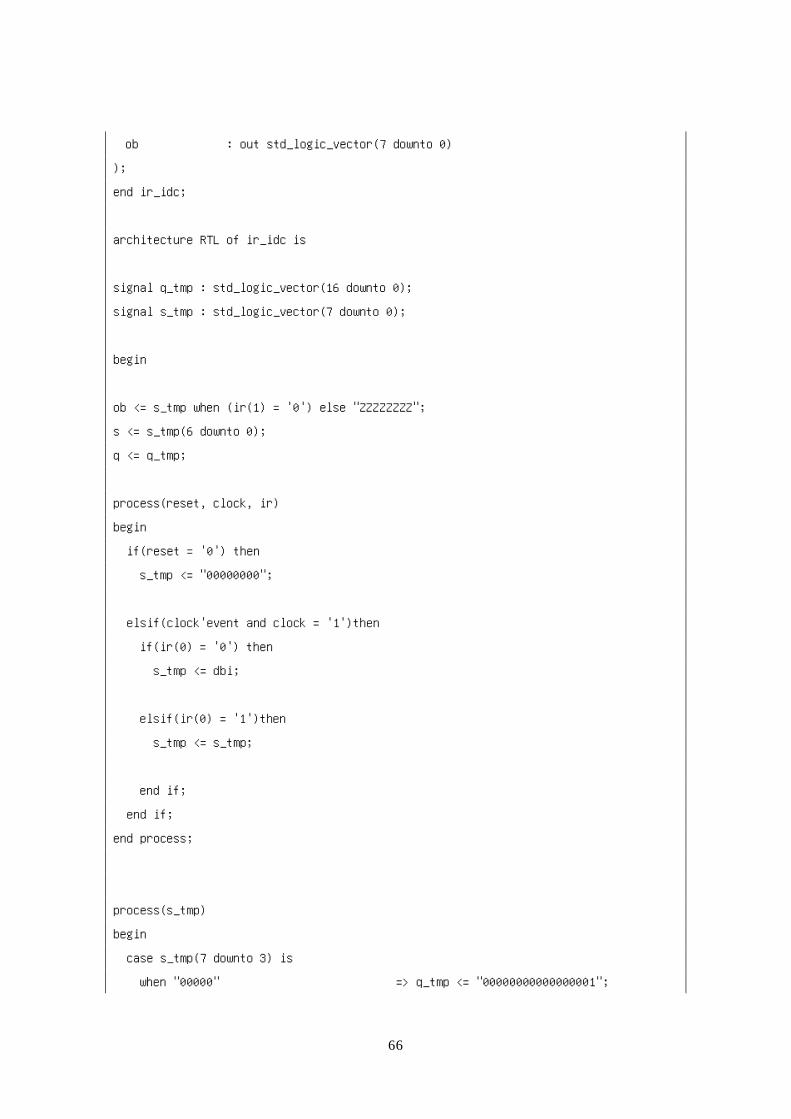
る。また、命令レジスタの内容は観測バス OB(0:7)で観測出来るようになっているので、コントローラからの信号 ir(1)に従い観測バス OB(0:7)に保持されているデータを出力する。命令レジスタ・命令デコーダの概要を図 3.3に示す。VHDL記述を付録 2-3に示す。
図 3.3 命令レジスタ・命令デコーダ概要
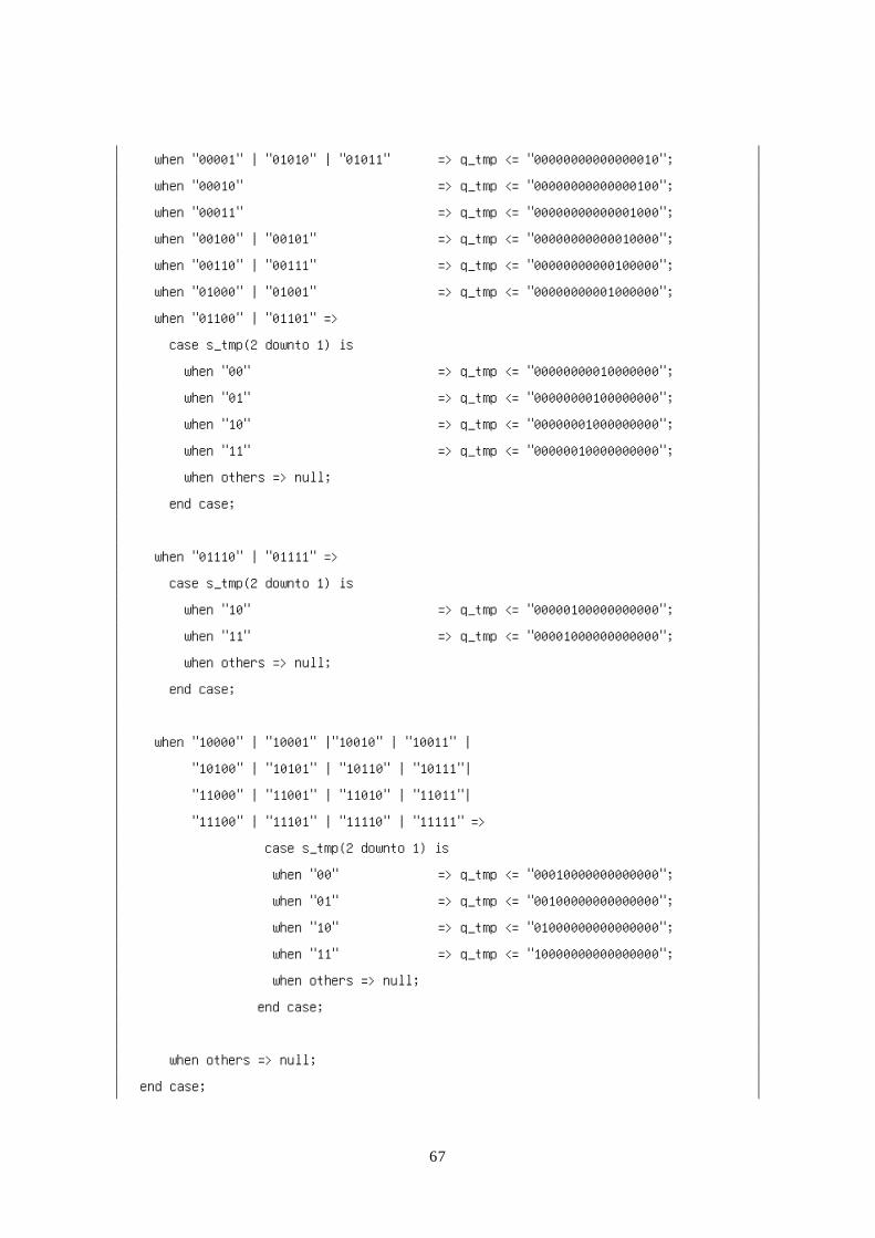
命令デコーダから出力される s(0:7)は、命令レジスタで保持されている命令コードの右から 1 ビット目から7ビット目を出力する。q(0:16)は命令コードを命令の種類ごとに 17種類に分けて出力する。例として命令レジスタに保持されている命令コードがNOP命令を表すものであったなら q(0)のみが1となり、qは(00000000000000001)となる。命令レジスタに保持された命令コードをどのように種類分けするのかを表 3.1に示す。
clock reset p(0:16)
s(0:6) ir(0:1) dbi(0:7) ob(0:7)
CONT.
CONT.へ
DBI_SET
KUE-CHIP2 出力 OBへ
17
表 3.1 命令デコーダの出力 q(0:16)の動作 q(0:16) 命令コード オペランド B
q(0) NOP
q(1) HLT
q(2) OUT
q(3) IN
q(4) RCF、 SCF
q(5) Bcc
q(6) SRA、SLA、SRL、SLL、RRA、RLA、RRL、RLL
q(7) LD ACC/IX
q(8) LD 即値アドレス
q(9) LD 絶対アドレス
q(10) LD インデックス修飾アドレス
q(11) ST 絶対アドレス
q(12) ST インデックス修飾アドレス
q(13) SBC、ADC、SUB、ADD、EOR、OR、AND、CMP ACC/IX
q(14) SBC、ADC、SUB、ADD、EOR、OR、AND、CMP 即値アドレス
q(15) SBC、ADC、SUB、ADD、EOR、OR、AND、CMP 絶対アドレス
q(16) SBC、ADC、SUB、ADD、EOR、OR、AND、CMP インデックス修飾アドレス
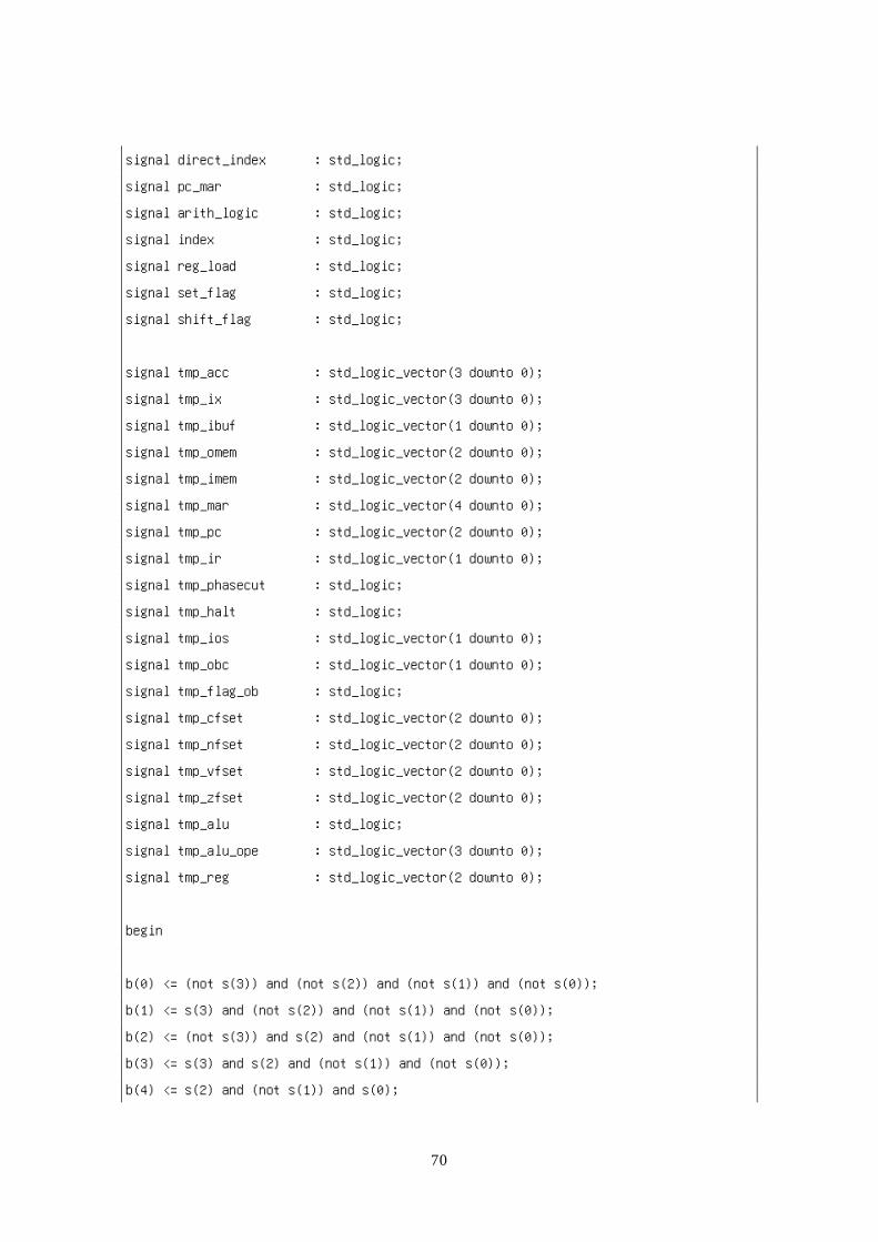
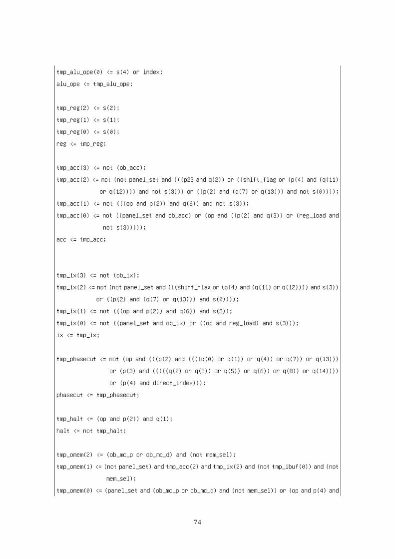
3.4 コントローラ設計
CISC アーキテクチャを採用している KUE-CHIP 2 では、コントローラからの制御信号をもとに各マクロが動作するので一番重要かつ、多くの入出力信
号が発生するため設計が困難な所である。コントローラの主な動作としては、
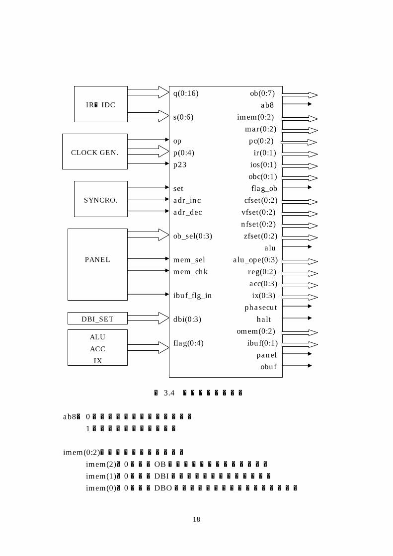
命令デコーダで解読された命令データである q(0:16)と s(0:6)、クロックジェネレータから発生する op信号とフェーズ信号 p(0:4)、KUE-CHIP 2のボード上からの入力信号、シンクロナイザからの信号、ALU・ACC・IXから発生したフラグ信号をもとに各マクロへの制御信号を発生させることである。図 3.4にコントローラの概要を示すとともに出力信号の機能を説明する。VHDL 記述を付録2-4に示す。
18
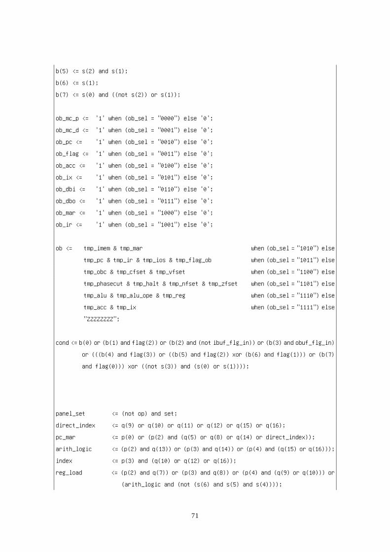
図 3.4 コントローラ概要
ab8: 0の時、プログラム領域を示す 1の時、データ領域を示す imem(0:2):内部メモリを制御する imem(2):0の時、OBに内部メモリのデータを出力 imem(1):0の時、DBIに内部メモリのデータを出力 imem(0):0の時、DBO上のデータを内部メモリに書き込む
q(0:16) ob(0:7) ab8 s(0:6) imem(0:2) mar(0:2) op pc(0:2) p(0:4) ir(0:1) p23 ios(0:1) obc(0:1) set flag_ob adr_inc cfset(0:2) adr_dec vfset(0:2) nfset(0:2) ob_sel(0:3) zfset(0:2) alu mem_sel alu_ope(0:3) mem_chk reg(0:2) acc(0:3) ibuf_flg_in ix(0:3) phasecut dbi(0:3) halt omem(0:2) flag(0:4) ibuf(0:1) panel obuf
IR・IDC
CLOCK GEN.
SYNCRO.
PANEL
ALU ACC IX
DBI_SET
19
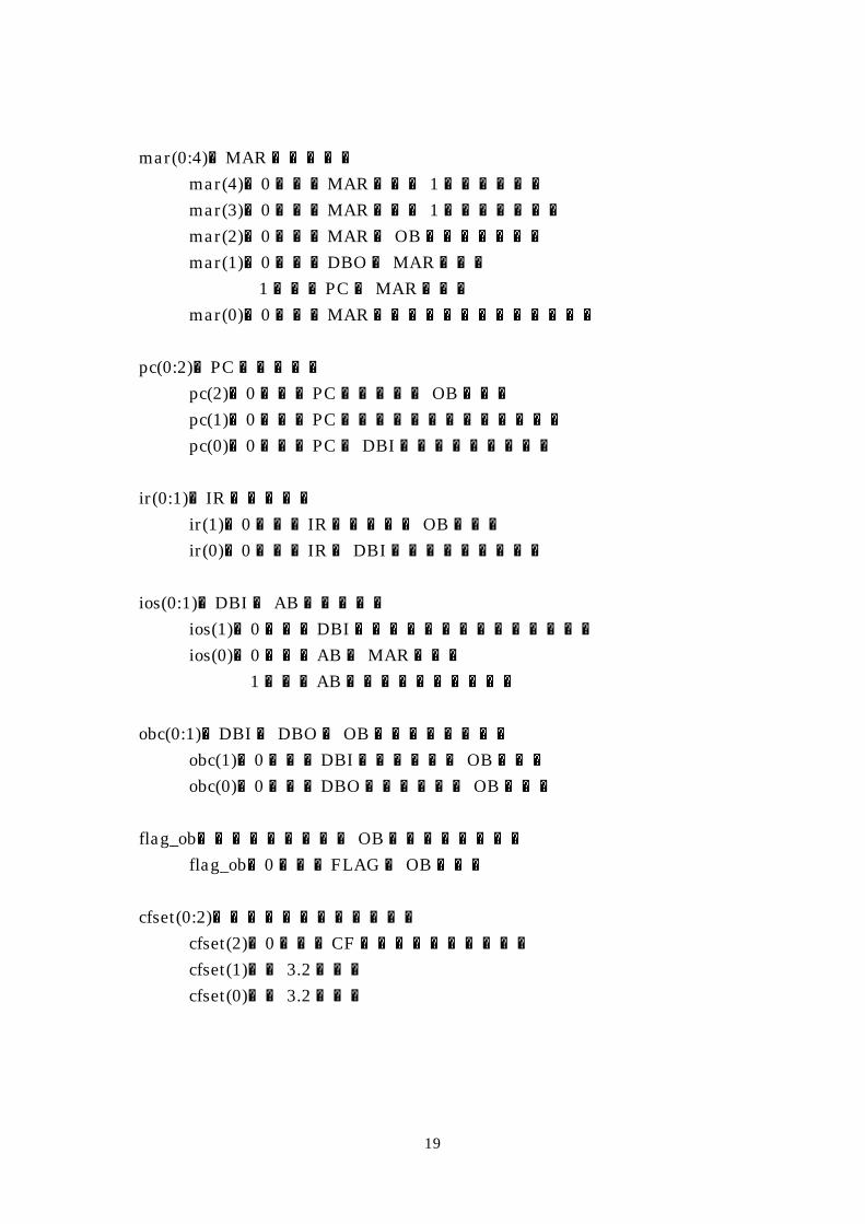
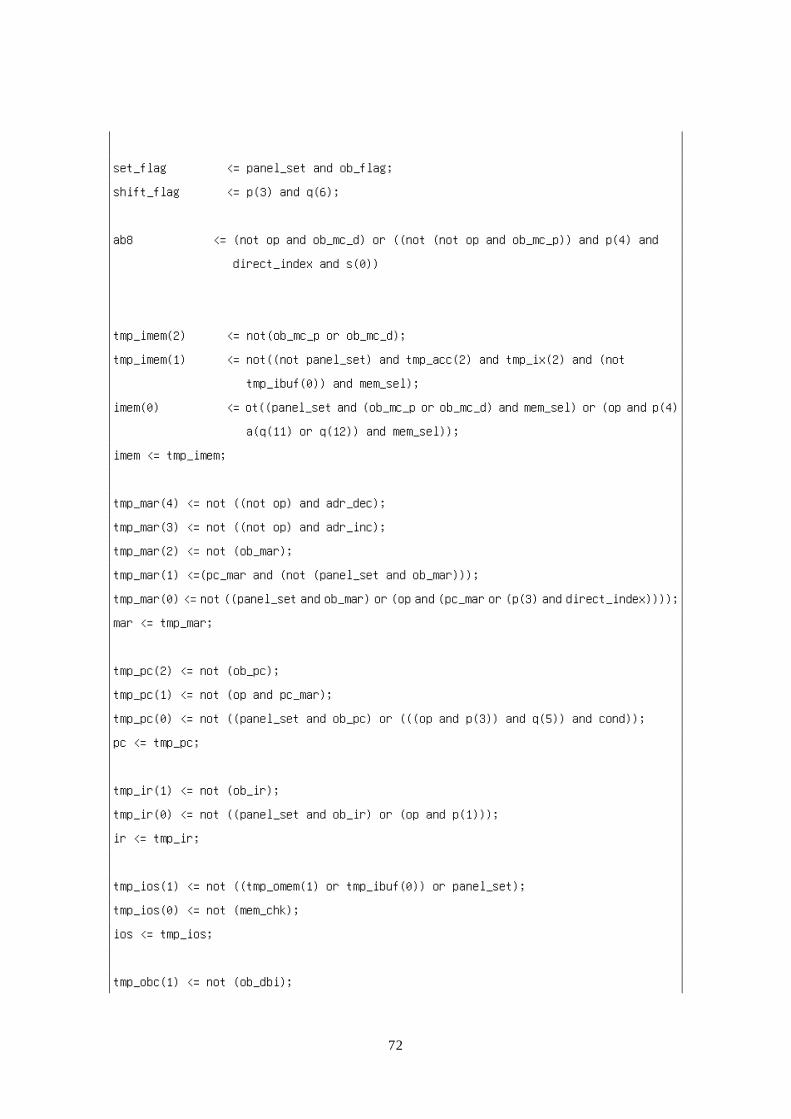
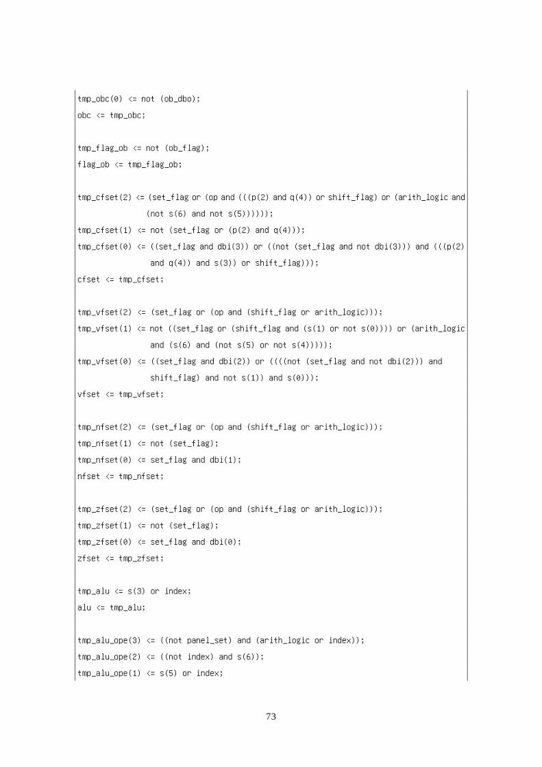
mar(0:4):MARを制御する mar(4):0の時、MARの値を 1デクリメント mar(3):0の時、MARの値を 1インクリメント mar(2):0の時、MARは OBにデータを出力 mar(1):0の時、DBOをMARに接続 1の時、PCをMARに接続 mar(0):0の時、MARは接続されたデータをラッチ pc(0:2):PCを制御する pc(2):0の時、PCはデータを OBに出力 pc(1):0の時、PCはデータを1インクリメント pc(0):0の時、PCは DBI上のデータをラッチ ir(0:1):IRを制御する ir(1):0の時、IRはデータを OBに出力 ir(0):0の時、IRは DBI上のデータをラッチ ios(0:1):DBIと ABを制御する ios(1):0の時、DBIはチップの外部から駆動される ios(0):0の時、ABはMARに接続 1の時、ABはチップ外部から駆動 obc(0:1):DBIと DBOを OBに出力させる信号 obc(1):0の時、DBI上のデータを OBへ出力 obc(0):0の時、DBO上のデータを OBへ出力 flag_ob:各フラグの状態を OBに出力させる信号 flag_ob:0の時、FLAGを OBへ出力 cfset(0:2):桁上げフラグを制御する cfset(2):0の時、CFはデータをラッチする cfset(1):表 3.2を参照 cfset(0):表 3.2を参照
20
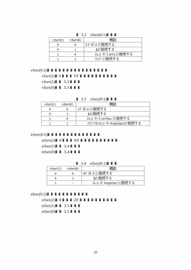
表 3.2 cfset(0:1)の機能 cfset(1) cfset(0) 機能
0 0 CF は 0 に接続する
0 1 1に接続する
1 0 ALU の Carry に接続する
1 1 TCF に接続する
vfset(0:2):オーバーフローフラグを制御する vfset(2):0の時、VFはデータをラッチする vfset(1):表 3.3を参照 vfset(0):表 3.3を参照
表 3.3 vfset(0:1)の機能 vfset(1) vfset(0) 機能
0 0 VF は 0 に接続する
0 1 1に接続する
1 0 ALU の Overflow に接続する
1 1 (TCF ALU の Negative)に接続する
nfset(0:2):ネガティブフラグを制御する nfset(2):0の時、NFはデータをラッチする nfset(1):表 3.4を参照 nfset(0):表 3.4を参照
表 3.4 nfset(0:1)の機能 nfset(1) nfset(0) 機能
0 0 NF は 0 に接続する
0 1 1に接続する
1 - ALU の Negative に接続する
zfset(0:2):ゼロフラグを制御する nfset(2):0の時、ZFはデータをラッチする nfset(1):表 3.5を参照 nfset(0):表 3.5を参照
21
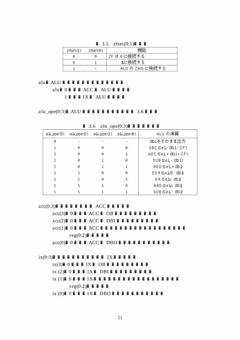
表 3.5 zfset(0:1)の機能 zfset(1) zfset(0) 機能
0 0 ZF は 0 に接続する
0 1 1に接続する
1 - ALU の Zero に接続する
alu:ALUにつなぐレジスタを選択する alu:0の時、ACCを ALUにつなぐ 1の時、IXを ALUにつなぐ alu_ope(0:3):ALUでの演算を指定する。表 3.6を参照
表 3.6 alu_ope(0:3)による演算指定 alu_ope(3) alu_ope(2) alu_ope(1) alu_ope(0) ALU の演算
0 - - - dbi をそのまま出力
1 0 0 0 SBC(Sel.- dbi - CF)
1 0 0 1 ADC(Sel. + dbi + CF)
1 0 1 0 SUB(Sel. - dbi )
1 0 1 1 ADD(Sel. + dbi)
1 1 0 0 EOR(Sel. dbi)
1 1 0 1 OR(Sel.∨dbi)
1 1 1 0 AND(Sel.∧dbi)
1 1 1 1 SUB(Sel. - dbi)
acc(0:3):アキュムレータ ACCを制御する acc(3):0の時、ACCは OBにデータを出力する acc(2):0の時、ACCは DBIにデータを出力する acc(1):0の時、ACCはデータをシフトする。シフトの種類は reg(0:2)で指定する acc(0):0の時、ACCは DBO上のデータをラッチする ix(0:3):インデックスレジスタ IXを制御する ix(3):0の時、IXは OBにデータを出力する ix (2):0の時、IXは DBIにデータを出力する ix (1):0の時、IXはデータをシフトする。シフトの種類は reg(0:2)で指定する ix (0):0の時、IXは DBO上のデータをラッチする
22
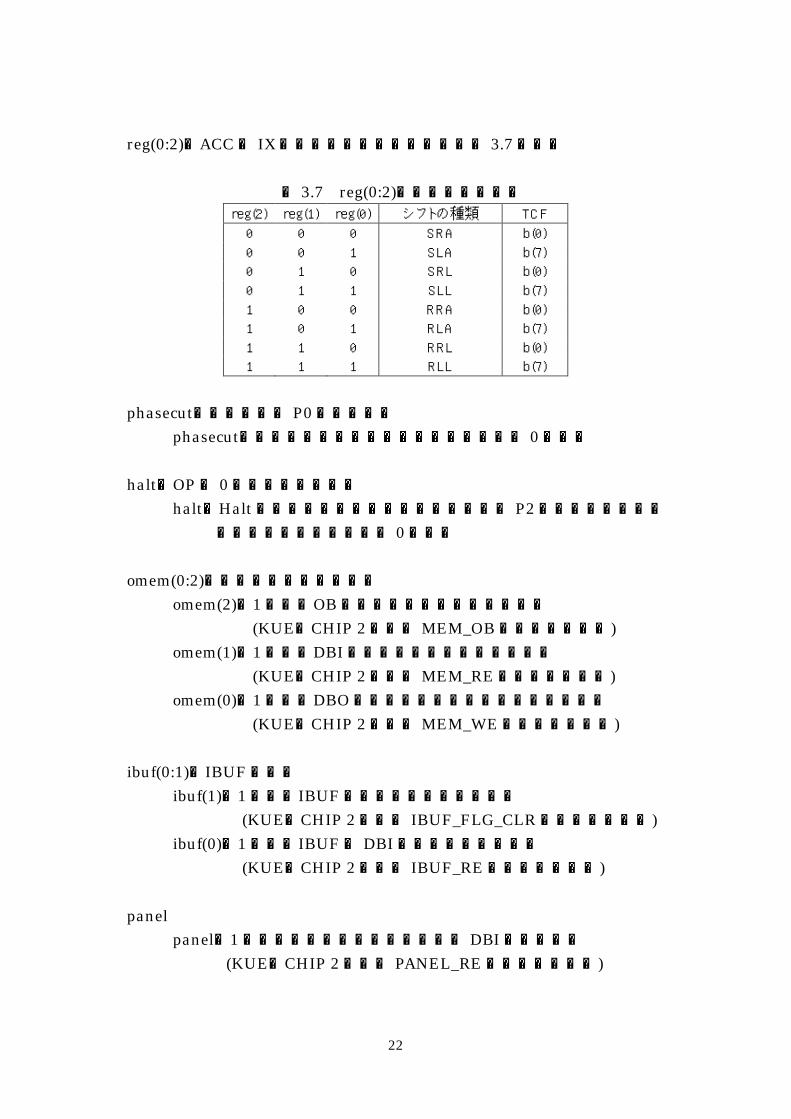
reg(0:2):ACCと IXで行うシフトを指定する。表 3.7を参照
表 3.7 reg(0:2)によるシフト指定 reg(2) reg(1) reg(0) シフトの種類 TCF
0 0 0 SRA b(0)
0 0 1 SLA b(7)
0 1 0 SRL b(0)
0 1 1 SLL b(7)
1 0 0 RRA b(0)
1 0 1 RLA b(7)
1 1 0 RRL b(0)
1 1 1 RLL b(7)
phasecut:フェーズを P0に戻す信号 phasecut:各命令実行最後のクロックフェーズで 0となる halt:OPを 0にセットする信号
halt:Halt命令実行の最後のクロックフェーズ P2もしくは各命令の 未定義フェーズのときに 0となる
omem(0:2):外部メモリを制御する omem(2):1の時、OBに外部メモリのデータを出力 (KUE-CHIP 2の出力MEM_OBに反転して接続) omem(1):1の時、DBIに外部メモリのデータを出力 (KUE-CHIP 2の出力MEM_REに反転して接続) omem(0):1の時、DBO上のデータを外部メモリに書き込む (KUE-CHIP 2の出力MEM_WEに反転して接続) ibuf(0:1):IBUFの制御 ibuf(1):1の時、IBUFのフラグをリセットする (KUE-CHIP 2の出力 IBUF_FLG_CLRに反転して接続) ibuf(0):1の時、IBUFは DBIにデータを出力する (KUE-CHIP 2の出力 IBUF_REに反転して接続) panel panel:1の時、データスイッチの内容を DBIに出力する (KUE-CHIP 2の出力 PANEL_REに反転して接続)
23
obuf obuf:0から 1に変化する際、DBOのデータを OBUFにセット (KUE-CHIP 2の出力 OBUF_WEに反転して接続)
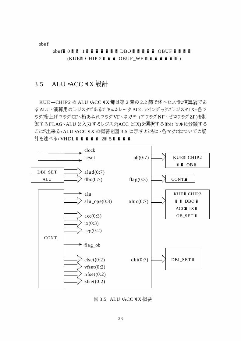
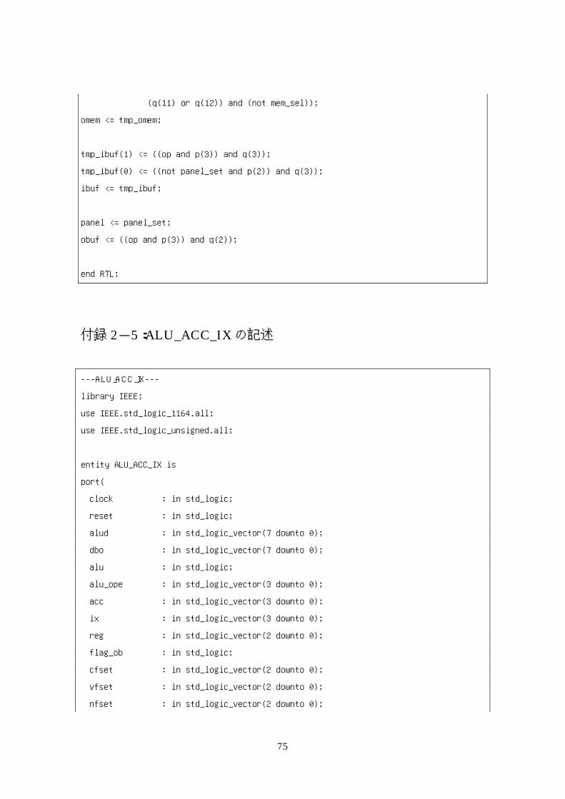
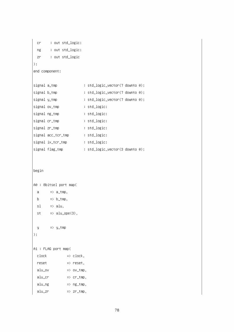
3.5 ALU・ACC・IX 設計
KUE-CHIP2 の ALU・ACC・IX 部は第 2 章の 2.2 節で述べたように演算器であ
る ALU、演算用のレジスタであるアキュムレータ ACC とインデックスレジスタ IX、各フ
ラグ(桁上げフラグ CF、桁あふれフラグ VF、ネガティブフラグ NF、ゼロフラグ ZF)を制
御する FLAG、ALU に入力するレジスタ(ACC と IX)を選択する 8bit セルに分類する
ことが出来る。ALU・ACC・IX の概要を図 3.5 に示すとともに、各マクロについての設
計を述べる。VHDL記述を付録 2-5に示す。
図 3.5 ALU・ACC・IX 概要
clock reset ob(0:7) alud(0:7) dbo(0:7) flag(0:3)
alu alu_ope(0:3) aluo(0:7) acc(0:3) ix(0:3) reg(0:2) flag_ob cfset(0:2) dbi(0:7) vfset(0:2) nfset(0:2) zfset(0:2)
CONT.
CONT.へ
KUE-CHIP2 出力 DBOへ ACC・IXへ OB_SETへ
DBI_SETへ
KUE-CHIP2 出力 OBへ
DBI_SET ALU
24
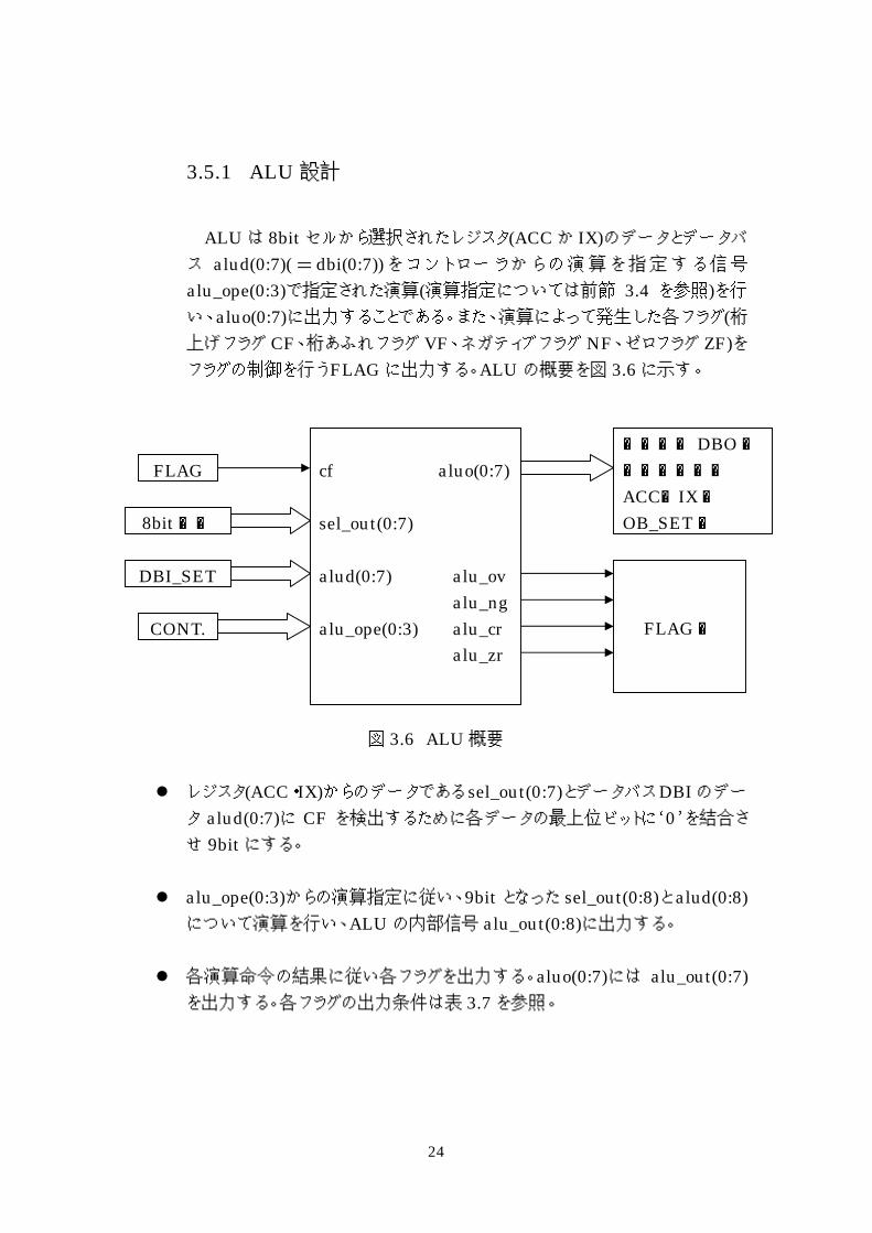
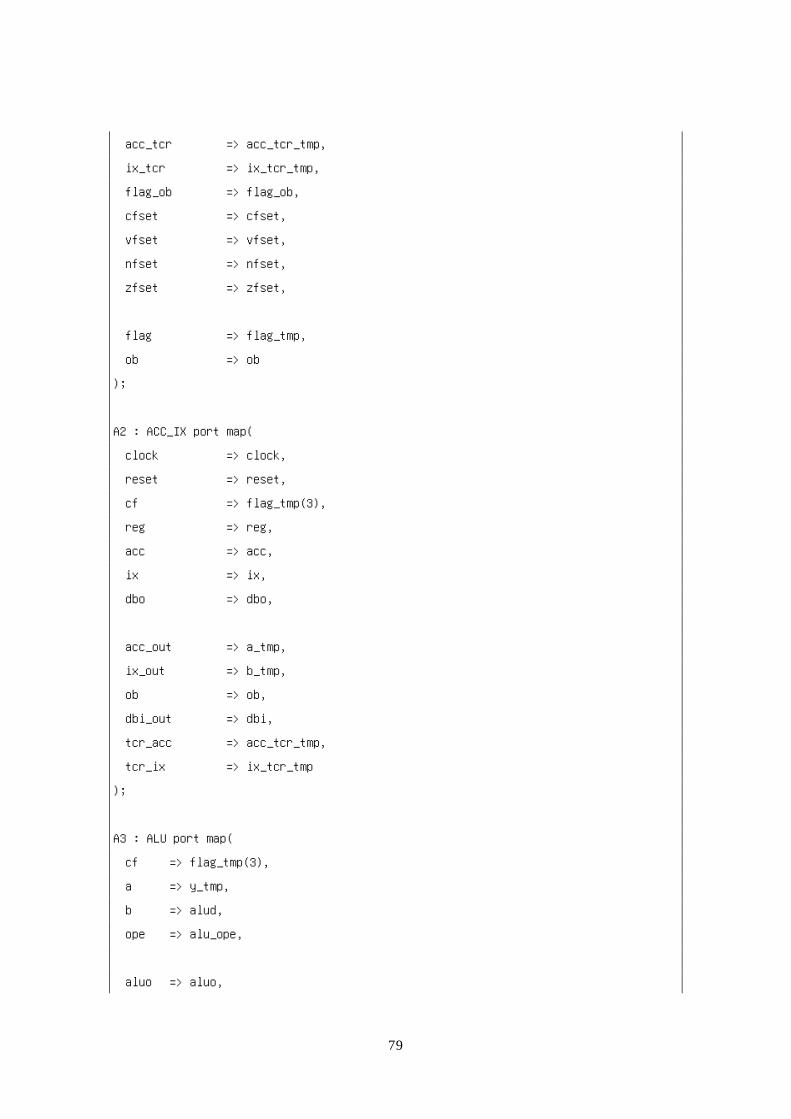
3.5.1 ALU 設計
ALU は 8bit セルから選択されたレジスタ(ACC か IX)のデータとデータバ
ス alud(0:7)( = dbi(0:7)) を コ ン ト ロ ー ラ か ら の 演 算 を 指 定 す る 信 号
alu_ope(0:3)で指定された演算(演算指定については前節 3.4 を参照)を行
い、aluo(0:7)に出力することである。また、演算によって発生した各フラグ(桁上げフラグ CF、桁あふれフラグ VF、ネガティブフラグ NF、ゼロフラグ ZF)をフラグの制御を行う FLAG に出力する。ALU の概要を図 3.6 に示す。
図 3.6 ALU 概要
レジスタ(ACC・IX)からのデータである sel_out(0:7)とデータバス DBI のデー
タ alud(0:7)に CF を検出するために各データの最上位ビットに‘0’を結合さ
せ 9bit にする。
alu_ope(0:3)からの演算指定に従い、9bit となった sel_out(0:8)と alud(0:8)について演算を行い、ALU の内部信号 alu_out(0:8)に出力する。
各演算命令の結果に従い各フラグを出力する。aluo(0:7)には alu_out(0:7)を出力する。各フラグの出力条件は表 3.7 を参照。
cf aluo(0:7) sel_out(0:7) alud(0:7) alu_ov alu_ng alu_ope(0:3) alu_cr alu_zr
8bitセル
DBI_SET
CONT.
FLAG 本体出力 DBOへ 内部メモリへ ACC・IXへ OB_SETへ
FLAGへ
25
表 3.7 フラグの機能 桁上げフラグ CF 桁あふれフラグ VF ネガティブフラグ NF ゼロフラグ ZF
SBC alu_out(8) V ※1 alu_out(7) Z ※3
ADC alu_out(8) V ※2 alu_out(7) Z ※3
SUB - V ※1 alu_out(7) Z ※3
ADD - V ※2 alu_out(7) Z ※3
EOR - 0 alu_out(7) Z ※3
OR - 0 alu_out(7) Z ※3
AND - 0 alu_out(7) Z ※3
CMP - V ※1 alu_out(7) Z ※3
- : 変化なし
※1 : sel_out(7) /= alud(7) かつ alud(7) = alu_out(7) の時 VF=’1’他の場合は VF=’0’
※2 : sel_out(7) = alud(7) かつ sel_data(7) /= alu_out(7)の時 VF=’1’他の場合は VF=’0’
※3 : alu_out(0:7)が”00000000”の時 ZF=’1’ 他の場合は ZF=’0’
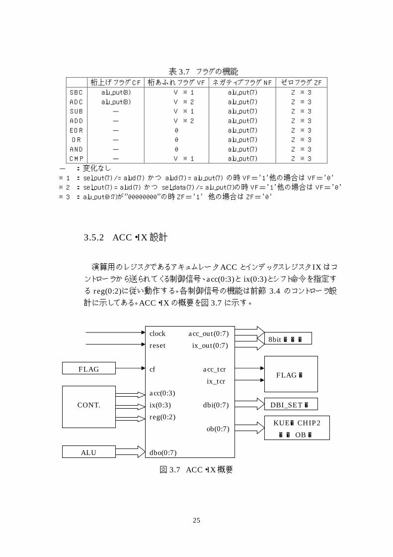
3.5.2 ACC・IX 設計
演算用のレジスタであるアキュムレータ ACC とインデックスレジスタ IX はコ
ントローラから送られてくる制御信号、acc(0:3)と ix(0:3)とシフト命令を指定す
る reg(0:2)に従い動作する。各制御信号の機能は前節 3.4 のコントローラ設
計に示してある。ACC・IX の概要を図 3.7 に示す。
図 3.7 ACC・IX 概要
clock acc_out(0:7) reset ix_out(0:7) cf acc_tcr ix_tcr acc(0:3) ix(0:3) dbi(0:7) reg(0:2)
ob(0:7) dbo(0:7)
FLAGへ
8bitセルへ
FLAG
CONT.
ALU
DBI_SETへ
KUE-CHIP2 出力 OBへ
26
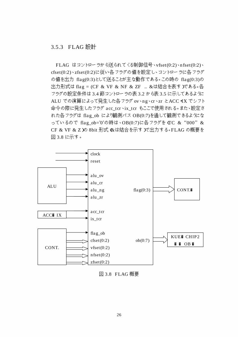
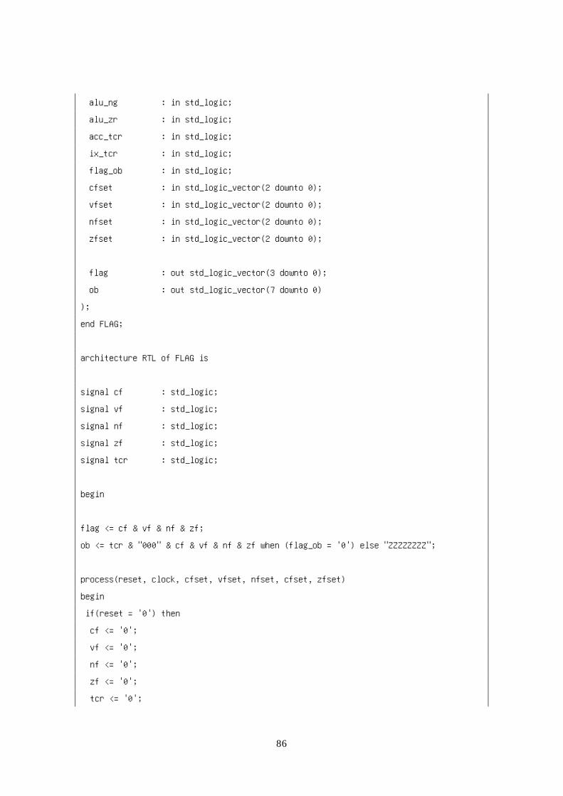
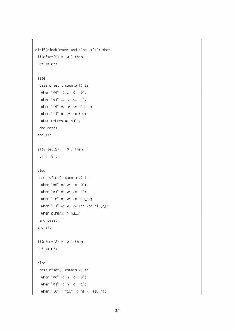
3.5.3 FLAG 設計
FLAG はコントローラから送られてくる制御信号、vfset(0:2)、nfset(0:2)、
cfset(0:2)、zfset(0:2)に従い各フラグの値を設定し、コントローラに各フラグ
の値を出力 flag(0:3)として送ることが主な動作である。この時の flag(0:3)の出力形式は flag = (CF & VF & NF & ZF …&は結合を表す)である。各
フラグの設定条件は 3.4 節コントローラの表 3.2 から表 3.5 に示してあるように
ALU での演算によって発生した各フラグ ov、ng、cr、zr と ACC・IX でシフト
命令の際に発生したフラグ acc_tcr、ix_tcr もここで使用される。また、設定さ
れた各フラグは flag_ob により観測バス OB(0:7)を通して観測できるようにな
っているので flag_ob=’0’の時は、OB(0:7)に各フラグを(TC & “000” & CF & VF & Z)の 8bit 形式(&は結合を示す)で出力する。FLAG の概要を
図 3.8 に示す。
図 3.8 FLAG 概要
clock reset alu_ov alu_cr alu_ng flag(0:3) alu_zr acc_tcr ix_tcr flag_ob cfset(0:2) ob(0:7) vfset(0:2) nfset(0:2) zfset(0:2)
ALU
ACC・IX
CONT.
CONT.へ
KUE-CHIP2 出力 OBへ
27
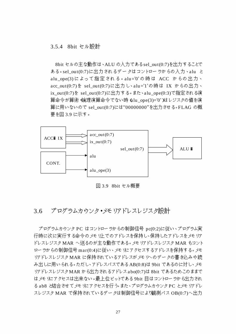
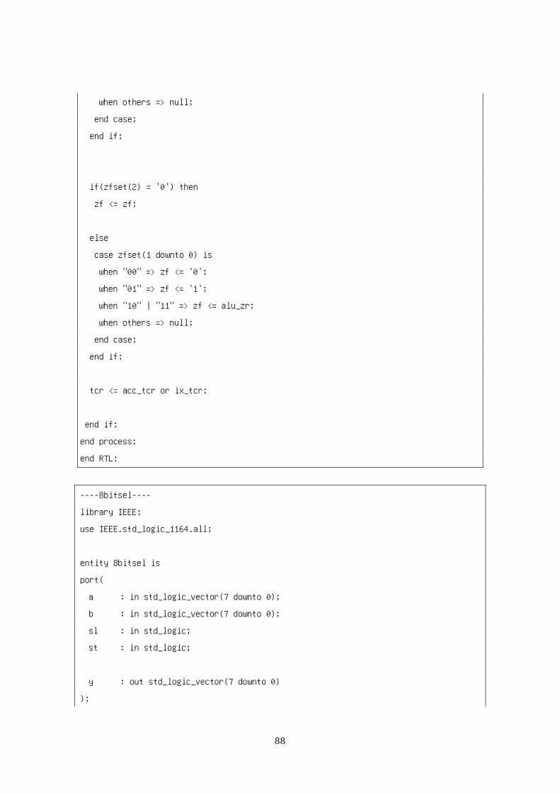
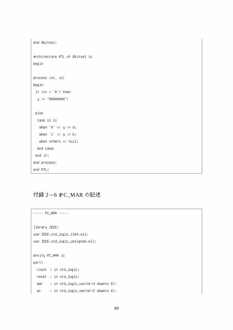
3.5.4 8bit セル設計
8bit セルの主な動作は、ALU の入力である sel_out(0:7)を出力することで
ある。sel_out(0:7)に出力されるデータはコントローラからの入力、alu と
alu_ope(3) に よ っ て 指 定 さ れ る 。 alu=’0’の 時 は ACC か ら の 出 力 、
acc_out(0:7)を sel_out(0:7)に出力し、alu=’1’の時は IX からの出力、
ix_out(0:7)を sel_out(0:7)に出力する。また、alu_ope(0:3)で指定される演
算命令が算術・論理演算命令でない時(alu_ope(3)=’0’)はレジスタの値を演
算に用いないので sel_out(0:7)には“00000000”を出力させる。FLAG の概
要を図 3.9 に示す。
図 3.9 8bit セル概要
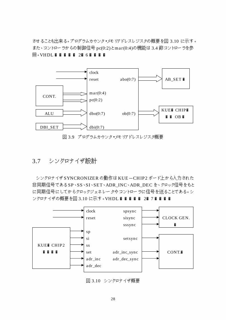
3.6 プログラムカウンタ・メモリアドレスレジスタ設計
プログラムカウンタ PC はコントローラからの制御信号 pc(0:2)に従い、プログラム実
行時に次に実行する命令のメモリ上でのアドレスを保持し、保持したアドレスをメモリア
ドレスレジスタ MAR へ送るのが主な動作である。メモリアドレスレジスタ MAR もコント
ローラからの制御信号 mar(0:4)に従い、メモリにアクセスするアドレスを保持する。メモ
リアドレスレジスタ MAR に保持されているアドレスがメモリへのデータの書き込みや読
み出しに用いられる。ただし、アドレスバスである AB(0:8)は 9bit であるのに対し、メモ
リアドレスレジスタ MAR から出力されるアドレス abo(0:7)は 8bit であるためこのままで
はメモリにアクセスは出来ない。最上位ビットである 9bit 目はコントローラから出力され
る ab8 と結合させてメモリにアクセスを行う。また、プログラムカウンタ PC とメモリアドレ
スレジスタ MAR で保持されているデータは制御信号により観測バス OB(0:7)へ出力
acc_out(0:7) ix_out(0:7) sel_out(0:7) alu alu_ope(3)
ACC・IX
CONT.
ALUへ
28
させることも出来る。プログラムカウンタ・メモリアドレスレジスタの概要を図 3.10 に示す。
また、コントローラからの制御信号 pc(0:2)と mar(0:4)の機能は 3.4 節コントローラを参
照。VHDL記述を付録 2-6に示す。
図 3.9 プログラムカウンタ・メモリアドレスレジスタ概要
3.7 シンクロナイザ設計
シンクロナイザ SYNCRONIZER の動作は KUE-CHIP2 ボード上から入力された
非同期信号である SP、SS、SI、SET、ADR_INC、ADR_DEC を、クロック信号をもと
に同期信号にしてからクロックジェネレータやコントローラに信号を送ることである。シ
ンクロナイザの概要を図 3.10 に示す。VHDL記述を付録 2-7に示す。
図 3.10 シンクロナイザ概要
clock reset abo(0:7) mar(0:4) pc(0:2) dbo(0:7) ob(0:7) dbi(0:7)
CONT.
ALU
AB_SETへ
DBI_SET
KUE-CHIP2 出力 OBへ
clock spsync reset sisync sssync sp si setsync ss set adr_inc_sync adr_inc adr_dec_sync adr_dec
CLOCK GEN.
へ
CONT.へ
KUE-CHIP2 ボード上
29
3.8 内部メモリ設計
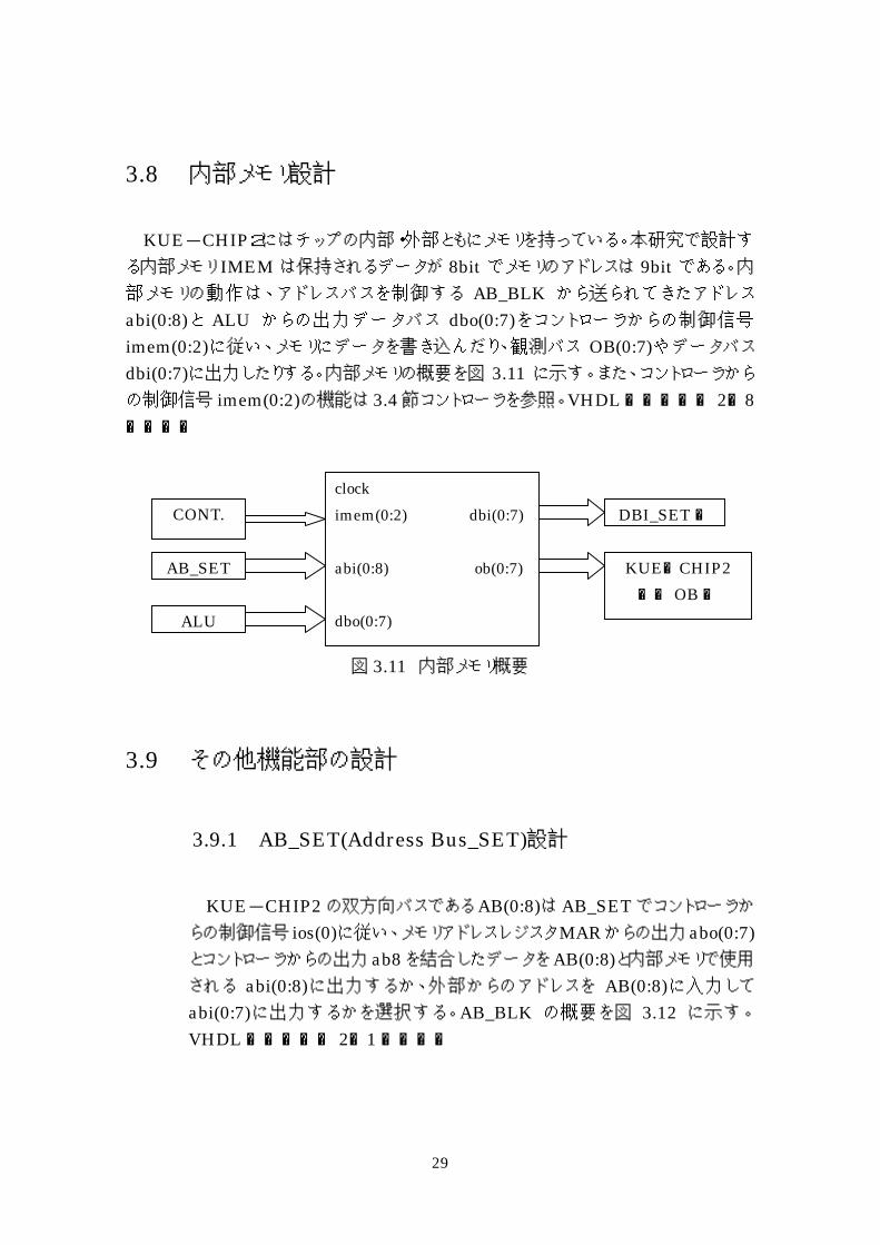
KUE-CHIP2にはチップの内部・外部ともにメモリを持っている。本研究で設計す
る内部メモリ IMEM は保持されるデータが 8bit でメモリのアドレスは 9bit である。内
部メモリの動作は、アドレスバスを制御する AB_BLK から送られてきたアドレス
abi(0:8)と ALU からの出力データバス dbo(0:7)をコントローラからの制御信号
imem(0:2)に従い、メモリにデータを書き込んだり、観測バス OB(0:7)やデータバス
dbi(0:7)に出力したりする。内部メモリの概要を図 3.11 に示す。また、コントローラから
の制御信号 imem(0:2)の機能は 3.4 節コントローラを参照。VHDL記述を付録 2-8に示す。
図 3.11 内部メモリ概要
3.9 その他機能部の設計
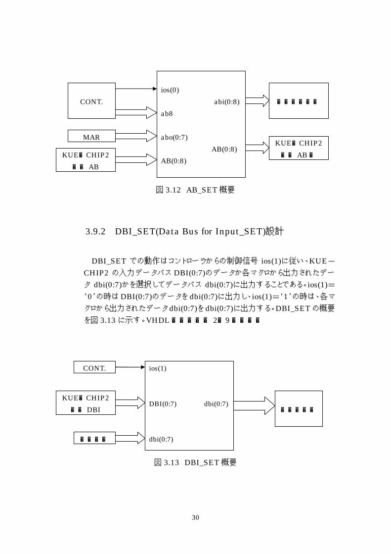
3.9.1 AB_SET(Address Bus_SET)設計
KUE-CHIP2 の双方向バスである AB(0:8)は AB_SET でコントローラか
らの制御信号 ios(0)に従い、メモリアドレスレジスタMARからの出力abo(0:7)とコントローラからの出力 ab8 を結合したデータを AB(0:8)と内部メモリで使用
される abi(0:8)に出力するか、外部からのアドレスを AB(0:8)に入力して
abi(0:7)に出力するかを選択する。AB_BLK の概要を図 3.12 に示す。
VHDL記述を付録 2-1に示す。
clock imem(0:2) dbi(0:7) abi(0:8) ob(0:7) dbo(0:7)
CONT.
AB_SET
ALU
DBI_SETへ
KUE-CHIP2 出力 OBへ
30
図 3.12 AB_SET 概要
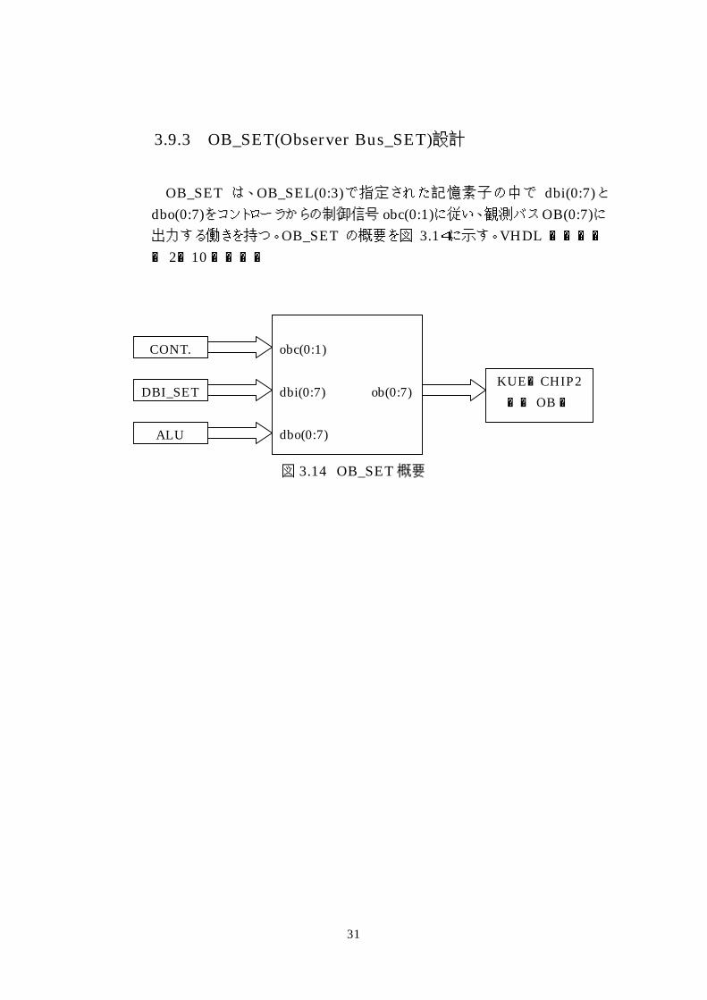
3.9.2 DBI_SET(Data Bus for Input_SET)設計
DBI_SET での動作はコントローラからの制御信号 ios(1)に従い、KUE-
CHIP2 の入力データバス DBI(0:7)のデータか各マクロから出力されたデー
タ dbi(0:7)かを選択してデータバス dbi(0:7)に出力することである。ios(1)=‘0’の時は DBI(0:7)のデータを dbi(0:7)に出力し、ios(1)=‘1’の時は、各マ
クロから出力されたデータ dbi(0:7)を dbi(0:7)に出力する。DBI_SET の概要
を図 3.13 に示す。VHDL記述を付録 2-9に示す。
図 3.13 DBI_SET 概要
ios(0) abi(0:8) ab8 abo(0:7)
AB(0:8) AB(0:8)
内部メモリへ
KUE-CHIP2 出力 ABへ
CONT.
MAR
KUE-CHIP2 入力 AB
ios(1) DBI(0:7) dbi(0:7) dbi(0:7)
各マクロへ
KUE-CHIP2 入力 DBI
CONT.
各マクロ
31
3.9.3 OB_SET(Observer Bus_SET)設計
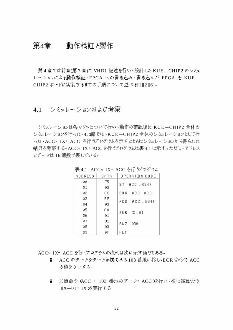
OB_SET は、OB_SEL(0:3)で指定された記憶素子の中で dbi(0:7)と
dbo(0:7)をコントローラからの制御信号 obc(0:1)に従い、観測バス OB(0:7)に出力する働きを持つ。OB_SET の概要を図 3.14に示す。VHDL 記述を付録 2-10に示す。
図 3.14 OB_SET 概要
obc(0:1) dbi(0:7) ob(0:7) dbo(0:7)
CONT.
DBI_SET
ALU
KUE-CHIP2 出力 OBへ
32
第4章 動作検証と製作
第 4 章では前章(第 3 章)で VHDL 記述を行い、設計した KUE-CHIP2 のシミュ
レーションによる動作検証、FPGA への書き込み、書き込んだ FPGA を KUE-
CHIP2 ボードに実装するまでの手順について述べる[1][2][6]。
4.1 シミュレーションおよび考察
シミュレーションは各マクロについて行い、動作の確認後に KUE-CHIP2 全体の
シミュレーションを行った。4.1節では、KUE-CHIP2 全体のシミュレーションとして行
った、ACC×IX→ACC を行うプログラムを示すとともにシミュレーションから得られた
結果を考察する。ACC×IX→ACCを行うプログラムは表4.1 に示す。ただし、アドレス
とデータは 16 進数で表している。
表 4.1 ACC×IX→ACC を行うプログラム ADDRESS DATA OPERATION CODE
00 75
01 03 ST ACC , (03H)
02 C0 EOR ACC , ACC
03 B5
04 03 ADD ACC , (03H)
05 AA
06 01 SUB IX , 01
07 31
08 03 BNZ 03H
09 0F HLT
ACC×IX→ACC を行うプログラムの流れは次に示す通りである。 ① ACC のデータをデータ領域である 103 番地に移し、EOR 命令で ACC
の値を 0 にする。 ② 加算命令(ACC + 103 番地のデータ→ACC)を行い、次に減算命令
(IX-01→IX)を実行する
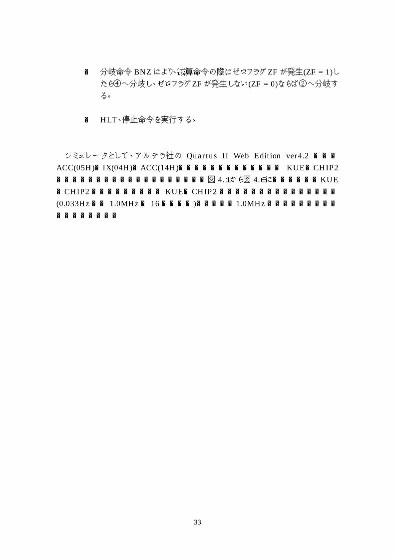
33
③ 分岐命令 BNZ により、減算命令の際にゼロフラグ ZF が発生(ZF = 1)したら④へ分岐し、ゼロフラグ ZF が発生しない(ZF = 0)ならば②へ分岐す
る。 ④ HLT、停止命令を実行する。
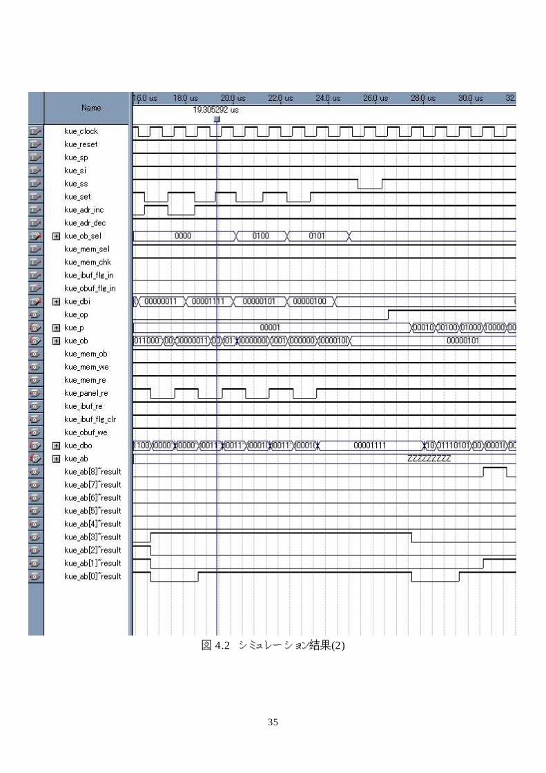
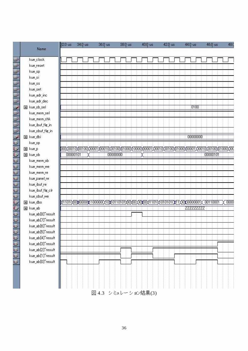
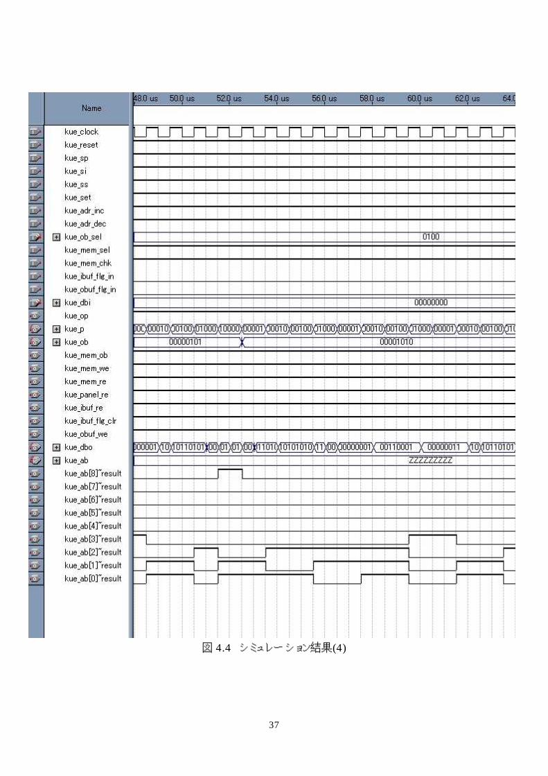
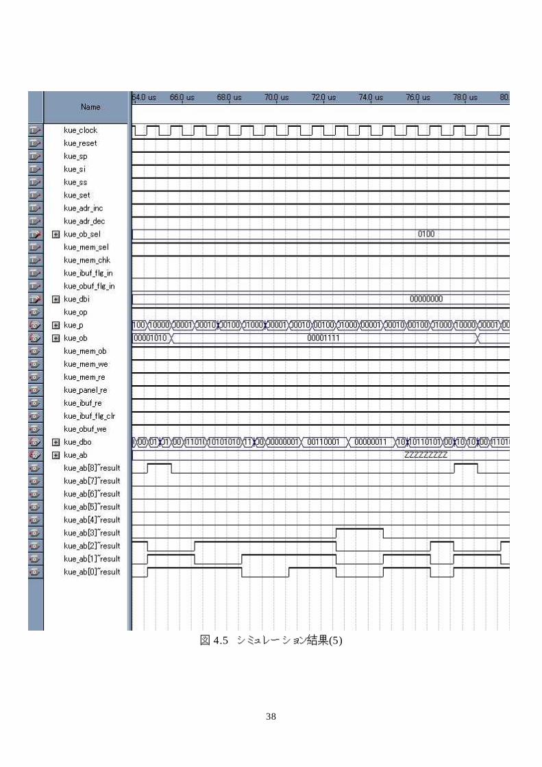
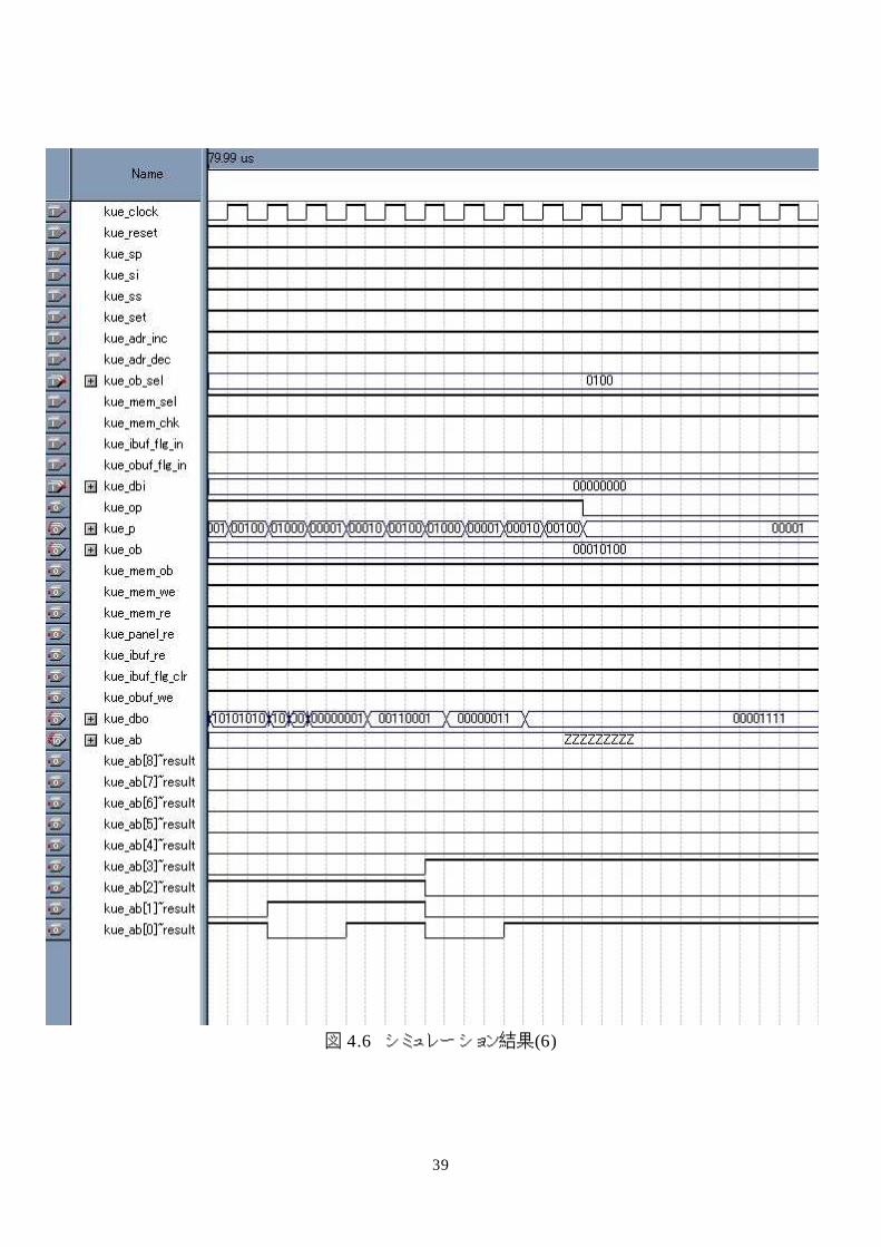
シミュレータとして、アルテラ社の Quartus II Web Edition ver4.2 を使いACC(05H)×IX(04H)→ACC(14H)を行うプログラムを設計した KUE-CHIP2に実行させた。シミュレーションの結果を図 4.1から図 4.6に示す。なお、KUE-CHIP2に与えたクロックは KUE-CHIP2ボードから送られてくるクロック(0.033Hzから 1.0MHzの 16段階可変)を考慮し、1.0MHzを与えてシミュレーションを行った。
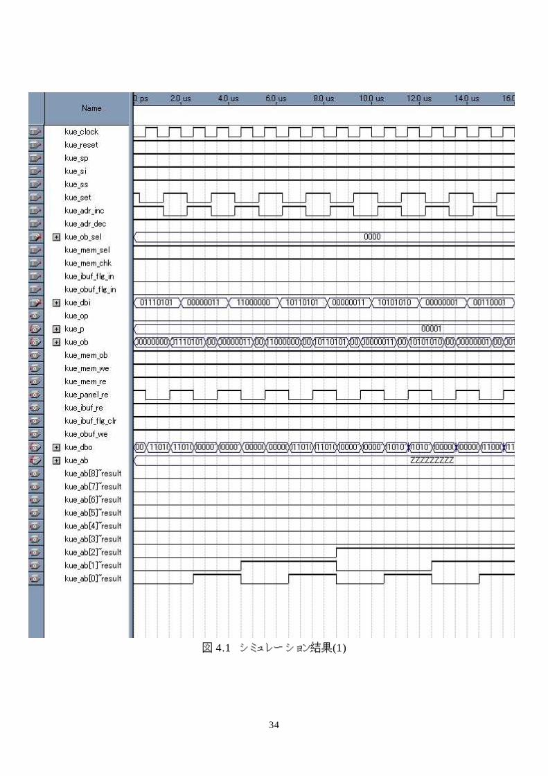
34
図 4.1 シミュレーション結果(1)
35
図 4.2 シミュレーション結果(2)
36
図 4.3 シミュレーション結果(3)
37
図 4.4 シミュレーション結果(4)
38
図 4.5 シミュレーション結果(5)
39
図 4.6 シミュレーション結果(6)
40
OB_SEL=“0100”とし、ACC の値を観測バス OB に出力するようにしてプログラム
を実行するとシ ミュレーショ ン結果 から 分か るように ACC は“00000101”→
“00000000”→“00000101”→“00001010”→“00001111”→“00010100”と変化し
動作は停止した。“00010100”は“20 = 14H”なので ACC(05H)×IX(04H)→ACC(14H)は正しく動作することを確認できた。
4.2 FPGA への書き込み
FPGA(CSP-017-20)への書き込みは、ダウンロードケーブルを用いて
FPGAに実装されている EPC2(コンフィグレーション用 ROM)に書き込むことで行った。コンパイラの際に確認した KUE-CHIP2の概要を表 4.2に示す。
表 4.2 設計した KUE-CHIP2 の概要 特徴 FLEX 10k20 144-Pin
設計した
KUE-CHIP2
I/O ピン数 102 62(60%)
ロジックセル 1,152 537(46%)
レジスタ 1,152 62(6%)
トータル RAM ビット数 12,288 4,096(33%)
4.3 FPGA のピン配置
設計した KUE-CHIP2 を書き込んだ FPGA、CSP-017-20 のピン配置を表
4.3 に示す。
表 4.3 CSP-017-20 のピン配置(1) ピン番号 ピン名 ピン番号 ピン名 ピン番号 ピン名
1~7 - 43 ADR_INC 86 AB(2)
8 DBI(1) 44 ADR_DEC 87 AB(1)
9 DBI(0) 45 - 88 AB(0)
10~11 - 46 OB_SEL(3) 89 -
12 PANEL_RE 47 OB_SEL(2) 90 MEM_WE
13 OB(0) 48 OB_SEL(1) 91 MEM_RE
14~16 - 49 OB_SEL(0) 92 MEM_OB
17 OB(1) 50 - 93~116 -
41
表 4.3 CSP-017-20 のピン配置(2) ピン番号 ピン名 ピン番号 ピン名 ピン番号 ピン名
18 OB(2) 51 MEM_SEL 117 DBO(6)
19 OB(3) 52~53 - 118 DBO(7)
20 OB(4) 54 RESET 119 DBO(5)
21 OB(5) 55 CLOCK 120 DBO(4)
22 OB(6) 56~58 - 121 DBO(3)
23 OB(7) 59 MEM_CHK 122~129 -
24~25 - 60 IBUF_FLG_IN 130 DBO(2)
26 OP 61 - 131 DBO(1)
27 P(0) 62 IBUF_FLG_CLR 132 DBO(0)
28 P(1) 63 IBUF_RE 133 DBI(7)
29 P(2) 64 OBUF_FLG_IN 134 -
30 P(3) 65 OBUF_WE 135 DBI(6)
31 P(4) 66~77 - 136 DBI(5)
32~36 - 78 AB(8) 137 DBI(4)
37 SS 79 AB(7) 138 DBI(3)
38 SI 80 AB(6) 139 -
39 SP 81 AB(5) 140 DBI(2)
40 - 82 AB(4) 141~144 -
41 SET 83 AB(3)
42 - 84~85 -
-:未使用
4.4 基板の設計
本研究で設計した KUE-CHIP2 を書き込んだ FPGA、CSP-017C(144ピン)と
KUE-CHIP2 のボード(84 ピン)を接続するためにアダプタボードを CadSoft 社の
プリント基板 CAD、EAGLE Light 版を使用して設計し、試作を行った。4.4 節では基
板の設計について述べる。
4.4.1 ライブラリの設計
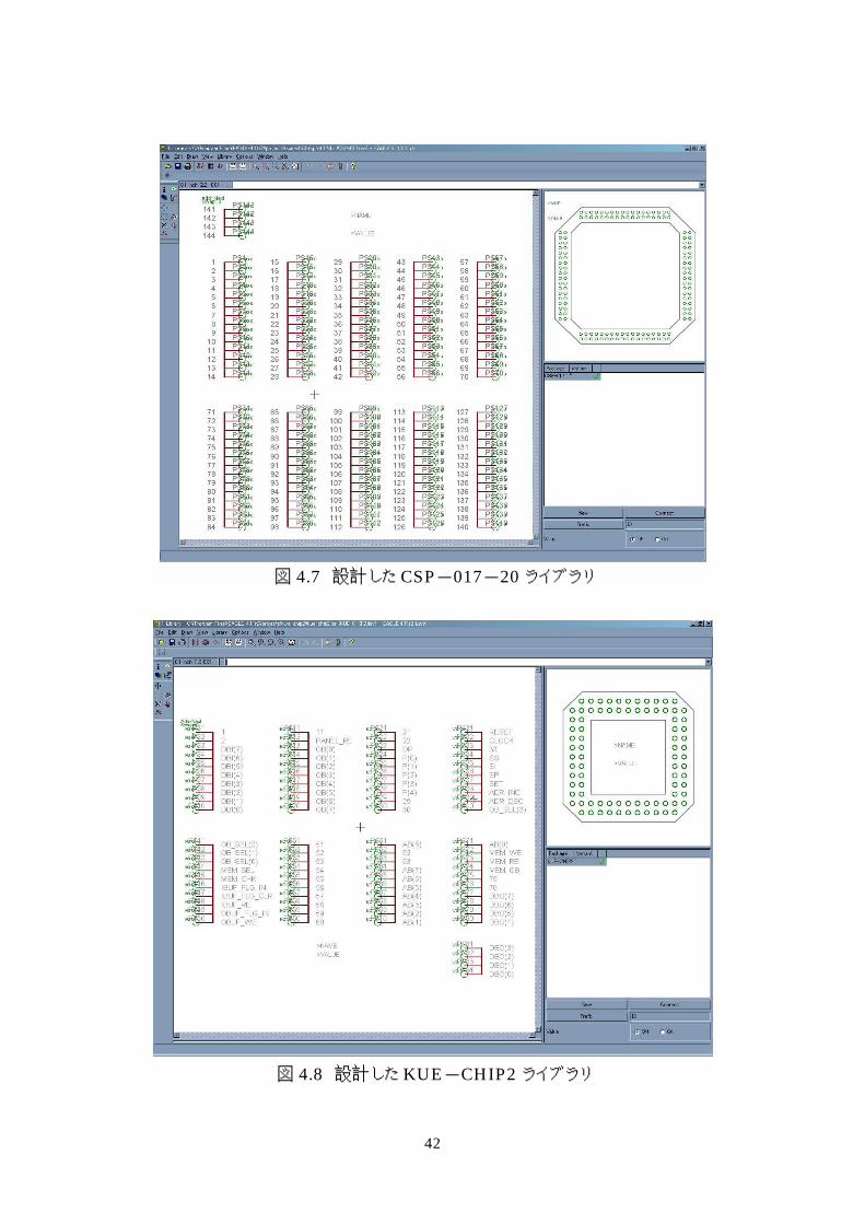
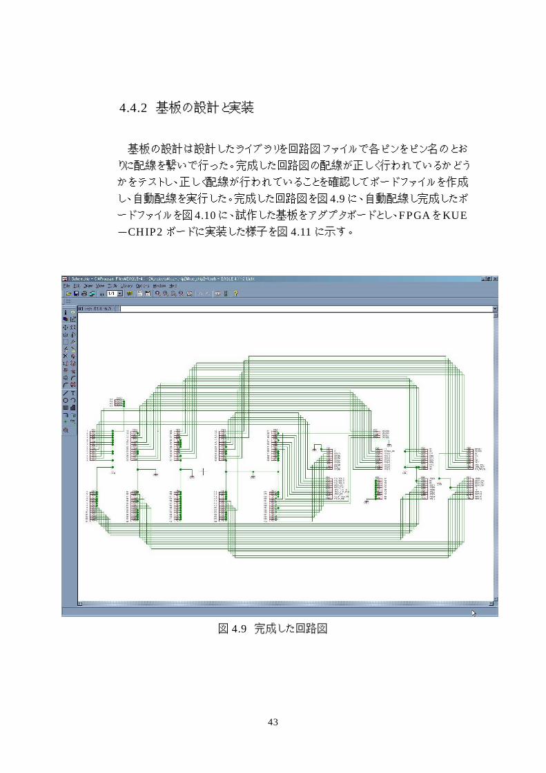
EAGLE Light 版には、144ピンと 84 ピンの IC ライブラリが見つからなか
ったので、144 ピンと 84 ピンのライブラリを第 2 章、表 2.5 の KUE-CHIP2のピン配置と表 5.1 の CSP-017-20 のピン配置をもとにして作成した。設
計した CSP-017-20 と KUE-CHIP2 のライブラリを図 4.7 と図 4.8 に示
す。
42
図 4.7 設計した CSP-017-20 ライブラリ
図 4.8 設計した KUE-CHIP2 ライブラリ
43
4.4.2 基板の設計と実装
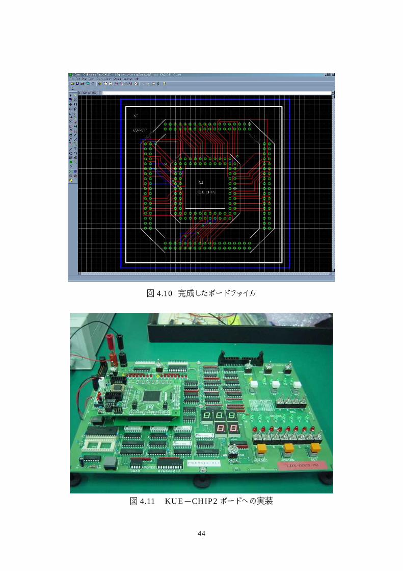
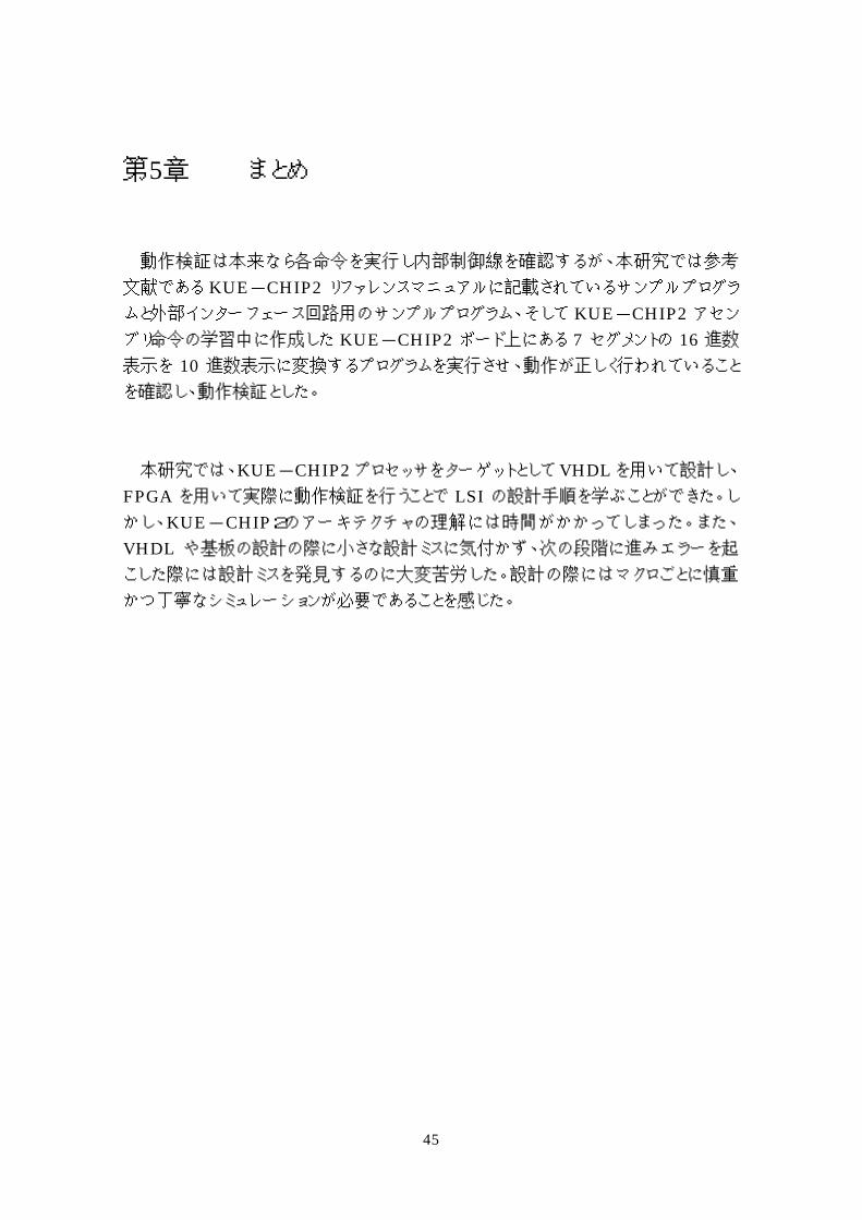
基板の設計は設計したライブラリを回路図ファイルで各ピンをピン名のとお
りに配線を繋いで行った。完成した回路図の配線が正しく行われているかどう
かをテストし、正しく配線が行われていることを確認してボードファイルを作成
し、自動配線を実行した。完成した回路図を図 4.9 に、自動配線し完成したボ
ードファイルを図4.10に、試作した基板をアダプタボードとし、FPGAをKUE-CHIP2 ボードに実装した様子を図 4.11 に示す。
図 4.9 完成した回路図
44
図 4.10 完成したボードファイル
図 4.11 KUE-CHIP2 ボードへの実装
45
第5章 まとめ
動作検証は本来なら各命令を実行し内部制御線を確認するが、本研究では参考
文献である KUE-CHIP2 リファレンスマニュアルに記載されているサンプルプログラ
ムと外部インターフェース回路用のサンプルプログラム、そして KUE-CHIP2 アセン
ブリ命令の学習中に作成した KUE-CHIP2 ボード上にある 7 セグメントの 16 進数
表示を 10 進数表示に変換するプログラムを実行させ、動作が正しく行われていること
を確認し、動作検証とした。 本研究では、KUE-CHIP2 プロセッサをターゲットとして VHDL を用いて設計し、
FPGA を用いて実際に動作検証を行うことで LSI の設計手順を学ぶことができた。し
かし、KUE-CHIP2のアーキテクチャの理解には時間がかかってしまった。また、
VHDL や基板の設計の際に小さな設計ミスに気付かず、次の段階に進みエラーを起
こした際には設計ミスを発見するのに大変苦労した。設計の際にはマクロごとに慎重
かつ丁寧なシミュレーションが必要であることを感じた。
46
謝辞 本研究を行うに際し、懇切丁寧な御指導、御鞭撻を賜りました高知工科大学
工学部電子・光システム工学科、矢野政顕教授に心から感謝致します。 研究中、懇切丁寧な御指導を賜りました高知工科大学工学部電子・光システ
ム工学科、原央教授ならびに橘昌良助教授、各先生方に厚く御礼申し上げます。 また、終始適切な助言、助力を頂きました谷脇史高氏、矢野研究室、原研究
室、橘研究室の同期生諸氏、他多くの方々に深く感謝するとともに心から御礼
申し上げます。
47
参考文献
[1] 神原弘之・越智裕之・澤田宏・浜口清治・岡田和久・上嶋明・安浦寛人 “KUE-CHIP 2設計ドキュメント” ASTEM RI/Kyoto (1994) [2] 神原弘之・越智裕之・澤田宏・浜口清治・岡田和久・上嶋明・安浦寛人
“KUE-CHIP 2リファレンスマニュアル” ASTEM RI/Kyoto (1994) [3] 柴山潔 “コンピュータアーキテクチャの基礎” 近代科学社 (2003) [4] 長谷川裕恭 “VHDLによるハードウェア設計入門” CQ出版社 (1995)
[5] 仲野巧 “VHDLによるマイクロプロセッサ設計入門” CQ出版社 (2002) [6] 今野邦彦 “プリント基板 CAD EAGLE活用入門” CQ出版社 (2004) [7] “KUE-CHIP2” http://www.metsa.astem.or.jp/kuechip2/ [8] “SYNOPSYSによる回路の合成手順”
http://www.vdec.u-tokyo.ac.jp/DesignLib/Kyushu/lecture/synopsys.html
48
付録 1
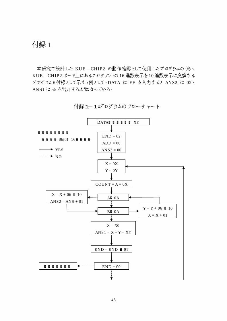
本研究で設計した KUE-CHIP2 の動作確認として使用したプログラムのうち、
KUE-CHIP2 ボード上にある 7 セグメントの 16 進数表示を 10 進数表示に変換する
プログラムを付録として示す。例として、DATA に FF を入力すると ANS2 に 02、
ANS1 に 55 を出力するようになっている。
付録1-1:プログラムのフローチャート
DATA=入力データ XY
X = 0X Y = 0Y
COUNT = A = 0X
A≧0A X = X + 06 -10
ANS2 = ANS + 01
B≧0A Y = Y + 06 -10
X = X + 01
X = X0 ANS1 = X + Y = XY
END = 02 ADD = 00 ANS2 = 00
END = END -01
END = 00 プログラム終了
※表示されている データは8bitの16進数表示
YES NO
49
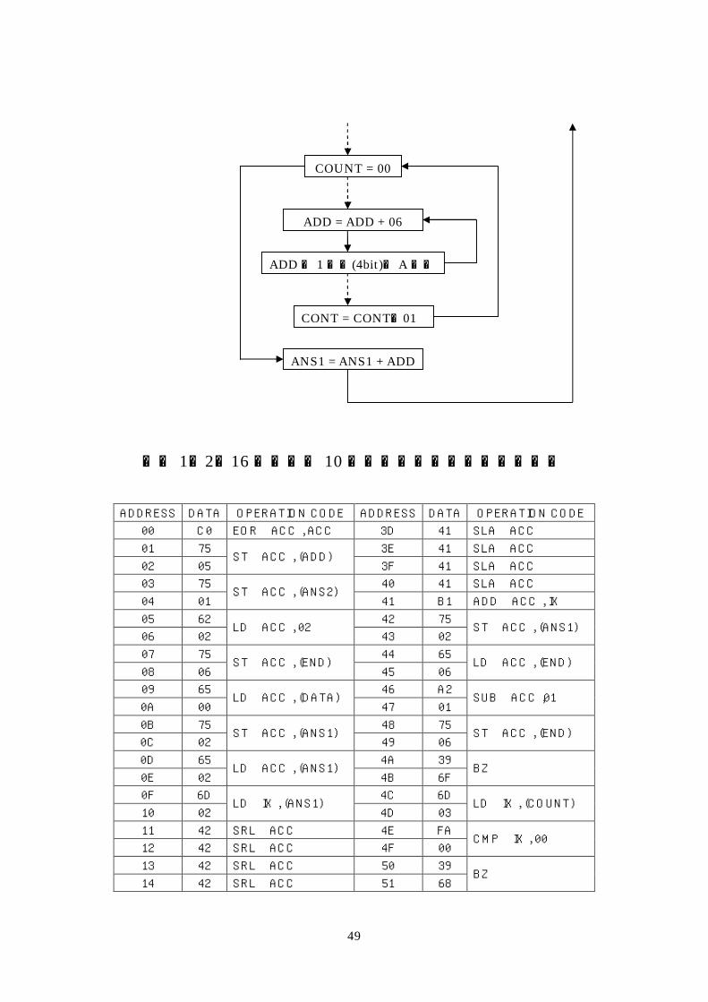
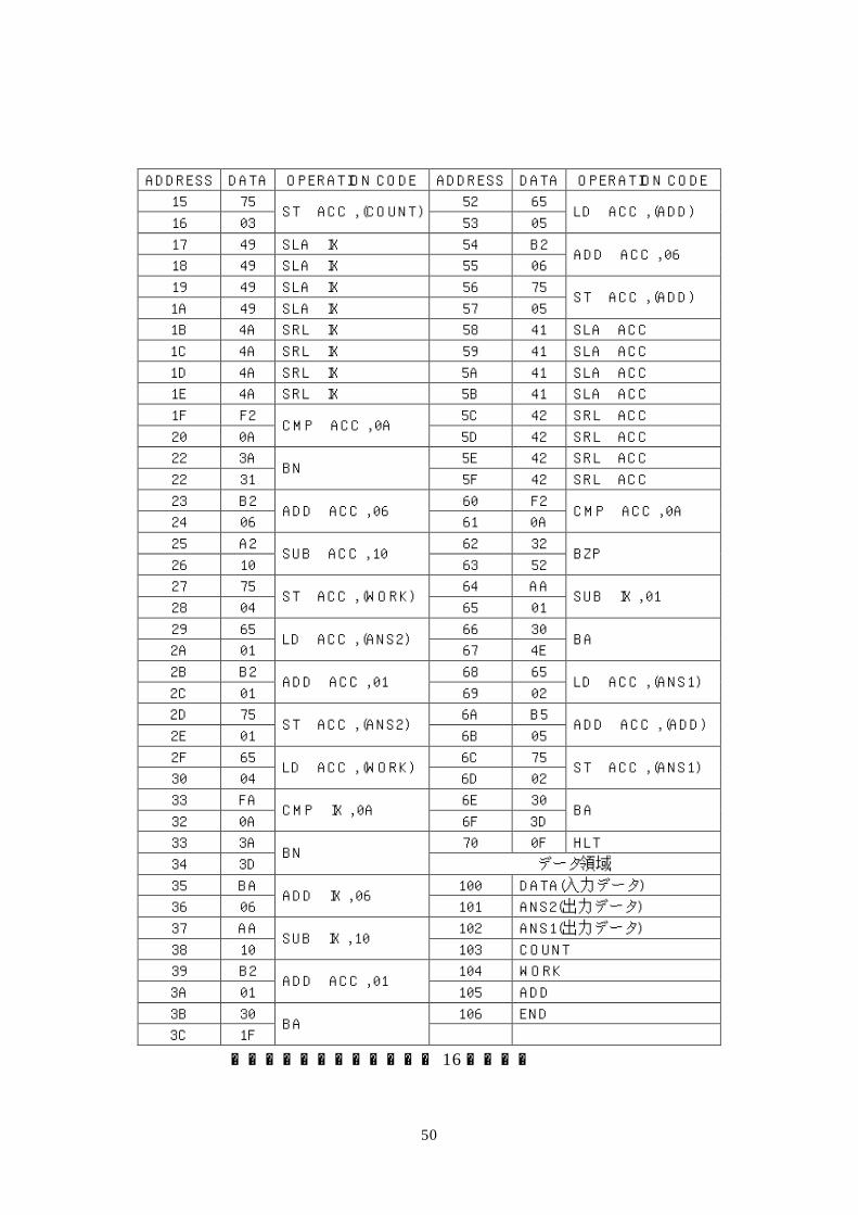
付録 1-2:16進表示を 10進表示に変換するプログラム
ADDRESS DATA OPERATION CODE ADDRESS DATA OPERATION CODE
00 C0 EOR ACC , ACC 3D 41 SLA ACC
01 75 3E 41 SLA ACC
02 05 ST ACC , (ADD)
3F 41 SLA ACC
03 75 40 41 SLA ACC
04 01 ST ACC , (ANS2)
41 B1 ADD ACC , IX
05 62 42 75
06 02 LD ACC , 02
43 02 ST ACC , (ANS1)
07 75 44 65
08 06 ST ACC , (END)
45 06 LD ACC , (END)
09 65 46 A2
0A 00 LD ACC , (DATA)
47 01 SUB ACC ,01
0B 75 48 75
0C 02 ST ACC , (ANS1)
49 06 ST ACC , (END)
0D 65 4A 39
0E 02 LD ACC , (ANS1)
4B 6F BZ
0F 6D 4C 6D
10 02 LD IX , (ANS1)
4D 03 LD IX , (COUNT)
11 42 SRL ACC 4E FA
12 42 SRL ACC 4F 00 CMP IX , 00
13 42 SRL ACC 50 39
14 42 SRL ACC 51 68 BZ
COUNT = 00
ADD = ADD + 06
ANS1 = ANS1 + ADD
ADDの 1桁目(4bit)が A以上
CONT = CONT-01
50
ADDRESS DATA OPERATION CODE ADDRESS DATA OPERATION CODE
15 75 52 65
16 03 ST ACC , (COUNT)
53 05 LD ACC , (ADD)
17 49 SLA IX 54 B2
18 49 SLA IX 55 06 ADD ACC , 06
19 49 SLA IX 56 75
1A 49 SLA IX 57 05 ST ACC , (ADD)
1B 4A SRL IX 58 41 SLA ACC
1C 4A SRL IX 59 41 SLA ACC
1D 4A SRL IX 5A 41 SLA ACC
1E 4A SRL IX 5B 41 SLA ACC
1F F2 5C 42 SRL ACC
20 0A CMP ACC , 0A
5D 42 SRL ACC
22 3A 5E 42 SRL ACC
22 31 BN
5F 42 SRL ACC
23 B2 60 F2
24 06 ADD ACC , 06
61 0A CMP ACC , 0A
25 A2 62 32
26 10 SUB ACC , 10
63 52 BZP
27 75 64 AA
28 04 ST ACC , (WORK)
65 01 SUB IX , 01
29 65 66 30
2A 01 LD ACC , (ANS2)
67 4E BA
2B B2 68 65
2C 01 ADD ACC , 01
69 02 LD ACC , (ANS1)
2D 75 6A B5
2E 01 ST ACC , (ANS2)
6B 05 ADD ACC , (ADD)
2F 65 6C 75
30 04 LD ACC , (WORK)
6D 02 ST ACC , (ANS1)
33 FA 6E 30
32 0A CMP IX , 0A
6F 3D BA
33 3A 70 0F HLT
34 3D BN
データ領域
35 BA 100 DATA(入力データ)
36 06 ADD IX , 06
101 ANS2(出力データ)
37 AA 102 ANS1(出力データ)
38 10 SUB IX , 10
103 COUNT
39 B2 104 WORK
3A 01 ADD ACC , 01
105 ADD
3B 30 106 END
3C 1F BA
※アドレス・データともに 16進数表示
51
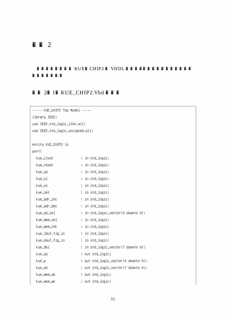
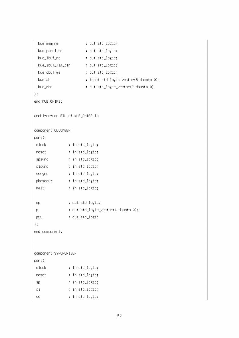
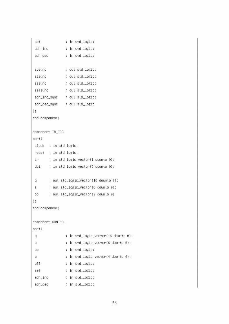
付録 2 本研究で設計した KUE-CHIP2の VHDL記述を、階層構造に従い以下に付録として示す。
付録 2-1:KUE_CHIP2.Vhdの記述
----- KUE_CHIP2 Top Model -----
library IEEE;
use IEEE.std_logic_1164.all;
use IEEE.std_logic_unsigned.all;
entity KUE_CHIP2 is
port(
kue_clock : in std_logic;
kue_reset : in std_logic;
kue_sp : in std_logic;
kue_si : in std_logic;
kue_ss : in std_logic;
kue_set : in std_logic;
kue_adr_inc : in std_logic;
kue_adr_dec : in std_logic;
kue_ob_sel : in std_logic_vector(3 downto 0);
kue_mem_sel : in std_logic;
kue_mem_chk : in std_logic;
kue_ibuf_flg_in : in std_logic;
kue_obuf_flg_in : in std_logic;
kue_dbi : in std_logic_vector(7 downto 0);
kue_op : out std_logic;
kue_p : out std_logic_vector(4 downto 0);
kue_ob : out std_logic_vector(7 downto 0);
kue_mem_ob : out std_logic;
kue_mem_we : out std_logic;
52
kue_mem_re : out std_logic;
kue_panel_re : out std_logic;
kue_ibuf_re : out std_logic;
kue_ibuf_flg_clr : out std_logic;
kue_obuf_we : out std_logic;
kue_ab : inout std_logic_vector(8 downto 0);
kue_dbo : out std_logic_vector(7 downto 0)
);
end KUE_CHIP2;
architecture RTL of KUE_CHIP2 is
component CLOCKGEN
port(
clock : in std_logic;
reset : in std_logic;
spsync : in std_logic;
sisync : in std_logic;
sssync : in std_logic;
phasecut : in std_logic;
halt : in std_logic;
op : out std_logic;
p : out std_logic_vector(4 downto 0);
p23 : out std_logic
);
end component;
component SYNCRONIZER
port(
clock : in std_logic;
reset : in std_logic;
sp : in std_logic;
si : in std_logic;
ss : in std_logic;
53
set : in std_logic;
adr_inc : in std_logic;
adr_dec : in std_logic;
spsync : out std_logic;
sisync : out std_logic;
sssync : out std_logic;
setsync : out std_logic;
adr_inc_sync : out std_logic;
adr_dec_sync : out std_logic
);
end component;
component IR_IDC
port(
clock : in std_logic;
reset : in std_logic;
ir : in std_logic_vector(1 downto 0);
dbi : in std_logic_vector(7 downto 0);
q : out std_logic_vector(16 downto 0);
s : out std_logic_vector(6 downto 0);
ob : out std_logic_vector(7 downto 0)
);
end component;
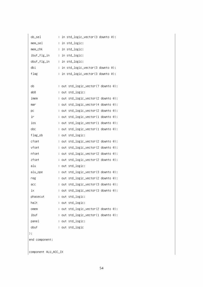
component CONTROL
port(
q : in std_logic_vector(16 downto 0);
s : in std_logic_vector(6 downto 0);
op : in std_logic;
p : in std_logic_vector(4 downto 0);
p23 : in std_logic;
set : in std_logic;
adr_inc : in std_logic;
adr_dec : in std_logic;
54
ob_sel : in std_logic_vector(3 downto 0);
mem_sel : in std_logic;
mem_chk : in std_logic;
ibuf_flg_in : in std_logic;
obuf_flg_in : in std_logic;
dbi : in std_logic_vector(3 downto 0);
flag : in std_logic_vector(3 downto 0);
ob : out std_logic_vector(7 downto 0);
ab8 : out std_logic;
imem : out std_logic_vector(2 downto 0);
mar : out std_logic_vector(4 downto 0);
pc : out std_logic_vector(2 downto 0);
ir : out std_logic_vector(1 downto 0);
ios : out std_logic_vector(1 downto 0);
obc : out std_logic_vector(1 downto 0);
flag_ob : out std_logic;
cfset : out std_logic_vector(2 downto 0);
vfset : out std_logic_vector(2 downto 0);
nfset : out std_logic_vector(2 downto 0);
zfset : out std_logic_vector(2 downto 0);
alu : out std_logic;
alu_ope : out std_logic_vector(3 downto 0);
reg : out std_logic_vector(2 downto 0);
acc : out std_logic_vector(3 downto 0);
ix : out std_logic_vector(3 downto 0);
phasecut : out std_logic;
halt : out std_logic;
omem : out std_logic_vector(2 downto 0);
ibuf : out std_logic_vector(1 downto 0);
panel : out std_logic;
obuf : out std_logic
);
end component;
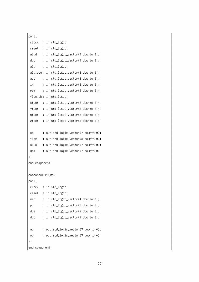
component ALU_ACC_IX
55
port(
clock : in std_logic;
reset : in std_logic;
alud : in std_logic_vector(7 downto 0);
dbo : in std_logic_vector(7 downto 0);
alu : in std_logic;
alu_ope : in std_logic_vector(3 downto 0);
acc : in std_logic_vector(3 downto 0);
ix : in std_logic_vector(3 downto 0);
reg : in std_logic_vector(2 downto 0);
flag_ob : in std_logic;
cfset : in std_logic_vector(2 downto 0);
vfset : in std_logic_vector(2 downto 0);
nfset : in std_logic_vector(2 downto 0);
zfset : in std_logic_vector(2 downto 0);
ob : out std_logic_vector(7 downto 0);
flag : out std_logic_vector(3 downto 0);
aluo : out std_logic_vector(7 downto 0);
dbi : out std_logic_vector(7 downto 0)
);
end component;
component PC_MAR
port(
clock : in std_logic;
reset : in std_logic;
mar : in std_logic_vector(4 downto 0);
pc : in std_logic_vector(2 downto 0);
dbi : in std_logic_vector(7 downto 0);
dbo : in std_logic_vector(7 downto 0);
ab : out std_logic_vector(7 downto 0);
ob : out std_logic_vector(7 downto 0)
);
end component;
56
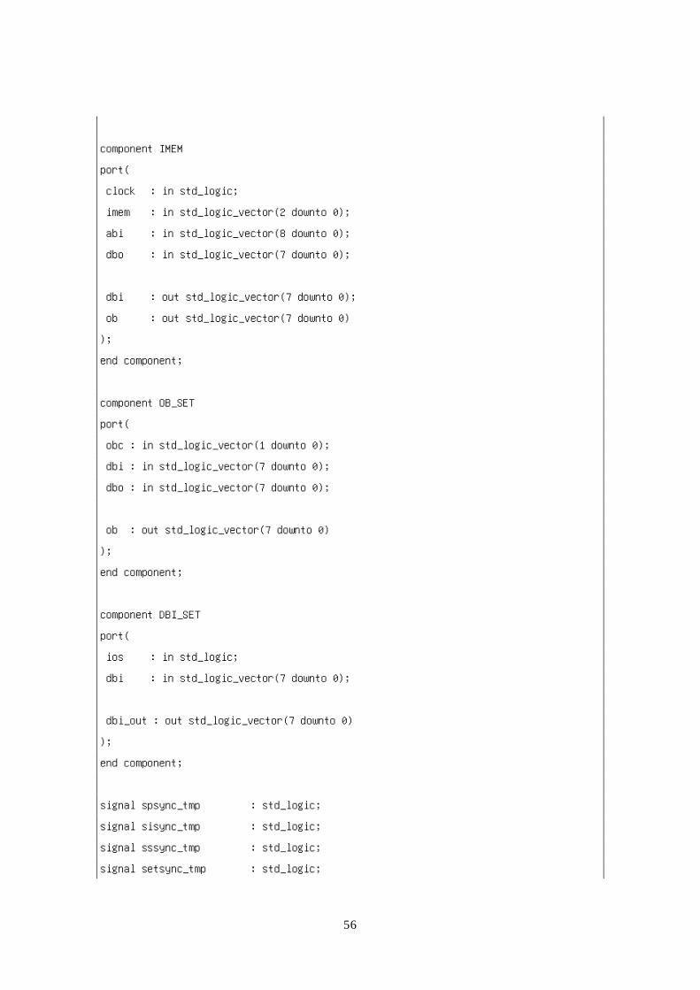
component IMEM
port(
clock : in std_logic;
imem : in std_logic_vector(2 downto 0);
abi : in std_logic_vector(8 downto 0);
dbo : in std_logic_vector(7 downto 0);
dbi : out std_logic_vector(7 downto 0);
ob : out std_logic_vector(7 downto 0)
);
end component;
component OB_SET
port(
obc : in std_logic_vector(1 downto 0);
dbi : in std_logic_vector(7 downto 0);
dbo : in std_logic_vector(7 downto 0);
ob : out std_logic_vector(7 downto 0)
);
end component;
component DBI_SET
port(
ios : in std_logic;
dbi : in std_logic_vector(7 downto 0);
dbi_out : out std_logic_vector(7 downto 0)
);
end component;
signal spsync_tmp : std_logic;
signal sisync_tmp : std_logic;
signal sssync_tmp : std_logic;
signal setsync_tmp : std_logic;
57
signal adr_inc_sync_tmp : std_logic;
signal adr_dec_sync_tmp : std_logic;
signal phasecut_tmp : std_logic;
signal halt_tmp : std_logic;
signal p23_tmp : std_logic;
signal p_tmp : std_logic_vector(4 downto 0);
signal op_tmp : std_logic;
signal ir_tmp : std_logic_vector(1 downto 0);
signal dbi_tmp : std_logic_vector(7 downto 0);
signal q_tmp : std_logic_vector(16 downto 0);
signal s_tmp : std_logic_vector(6 downto 0);
signal flag_tmp : std_logic_vector(3 downto 0);
signal ab8_tmp : std_logic;
signal imem_tmp : std_logic_vector(2 downto 0);
signal mar_tmp : std_logic_vector(4 downto 0);
signal pc_tmp : std_logic_vector(2 downto 0);
signal ios_tmp : std_logic_vector(1 downto 0);
signal obc_tmp : std_logic_vector(1 downto 0);
signal flag_ob_tmp : std_logic;
signal cfset_tmp : std_logic_vector(2 downto 0);
signal vfset_tmp : std_logic_vector(2 downto 0);
signal nfset_tmp : std_logic_vector(2 downto 0);
signal zfset_tmp : std_logic_vector(2 downto 0);
signal alu_tmp : std_logic;
signal alu_ope_tmp : std_logic_vector(3 downto 0);
signal reg_tmp : std_logic_vector(2 downto 0);
signal acc_tmp : std_logic_vector(3 downto 0);
signal ix_tmp : std_logic_vector(3 downto 0);
signal dbo_tmp : std_logic_vector(7 downto 0);
signal dbi_in : std_logic_vector(7 downto 0);
signal abo : std_logic_vector(7 downto 0);
signal abi : std_logic_vector(8 downto 0);
signal omem_tmp : std_logic_vector(2 downto 0);
signal ibuf_tmp : std_logic_vector(1 downto 0);
signal panel_tmp : std_logic;
signal obuf_tmp : std_logic;
58
begin
U0 : CLOCKGEN port map(
clock => kue_clock,
reset => kue_reset,
spsync => spsync_tmp,
sisync => sisync_tmp,
sssync => sssync_tmp,
phasecut => phasecut_tmp,
halt => halt_tmp,
op => op_tmp,
p => p_tmp,
p23 => p23_tmp
);
U1 : SYNCRONIZER port map(
clock => kue_clock,
reset => kue_reset,
sp => kue_sp,
si => kue_si,
ss => kue_ss,
set => kue_set,
adr_inc => kue_adr_inc,
adr_dec => kue_adr_dec,
spsync => spsync_tmp,
sisync => sisync_tmp,
sssync => sssync_tmp,
setsync => setsync_tmp,
adr_inc_sync => adr_inc_sync_tmp,
adr_dec_sync => adr_dec_sync_tmp
);
U2 : IR_IDC port map(
clock => kue_clock,
59
reset => kue_reset,
ir => ir_tmp,
dbi => dbi_in,
q => q_tmp,
s => s_tmp,
ob => kue_ob
);
U3 : CONTROL port map(
q => q_tmp,
s => s_tmp,
op => op_tmp,
p => p_tmp,
p23 => p23_tmp,
set => setsync_tmp,
adr_inc => adr_inc_sync_tmp,
adr_dec => adr_dec_sync_tmp,
ob_sel => kue_ob_sel,
mem_sel => kue_mem_sel,
mem_chk => kue_mem_chk,
ibuf_flg_in => kue_ibuf_flg_in,
obuf_flg_in => kue_obuf_flg_in,
dbi => dbi_in(3 downto 0),
flag => flag_tmp,
ob => kue_ob,
ab8 => ab8_tmp,
imem => imem_tmp,
mar => mar_tmp,
pc => pc_tmp,
ir => ir_tmp,
ios => ios_tmp,
obc => obc_tmp,
flag_ob => flag_ob_tmp,
cfset => cfset_tmp,
60
vfset => vfset_tmp,
nfset => nfset_tmp,
zfset => zfset_tmp,
alu => alu_tmp,
alu_ope => alu_ope_tmp,
reg => reg_tmp,
acc => acc_tmp,
ix => ix_tmp,
phasecut => phasecut_tmp,
halt => halt_tmp,
omem => omem_tmp,
ibuf => ibuf_tmp,
panel => panel_tmp,
obuf => obuf_tmp
);
U4 : ALU_ACC_IX port map(
clock => kue_clock,
reset => kue_reset,
alud => dbi_in,
dbo => dbo_tmp,
alu => alu_tmp,
alu_ope => alu_ope_tmp,
acc => acc_tmp,
ix => ix_tmp,
reg => reg_tmp,
flag_ob => flag_ob_tmp,
cfset => cfset_tmp,
vfset => vfset_tmp,
nfset => nfset_tmp,
zfset => zfset_tmp,
ob => kue_ob,
flag => flag_tmp,
aluo => dbo_tmp,
dbi => dbi_in
61
);
U5 : PC_MAR port map(
clock => kue_clock,
reset => kue_reset,
mar => mar_tmp,
pc => pc_tmp,
dbi => dbi_in,
dbo => dbo_tmp,
ab => abo,
ob => kue_ob
);
U6 : IMEM port map(
clock => kue_clock,
imem => imem_tmp,
abi => abi,
dbo => dbo_tmp,
dbi => dbi_in,
ob => kue_ob
);
U7 : OB_SET port map(
obc => obc_tmp,
dbi => dbi_in,
dbo => dbo_tmp,
ob => kue_ob
);
U8 : DBI_SET port map(
ios => ios_tmp(1),
dbi => kue_dbi,
62
dbi_out => dbi_in
);
-- AB_SET --
process(ios_tmp(0))
begin
if(ios_tmp(0) = '0')then
kue_ab <= ab8_tmp & abo;
abi <= ab8_tmp & abo;
elsif(ios_tmp(0) = '1')then
abi <= kue_ab;
kue_ab <= "ZZZZZZZZZ";
end if;
end process;
-- others --
kue_mem_ob <= not omem_tmp(2);
kue_mem_re <= not omem_tmp(1);
kue_mem_we <= not omem_tmp(0);
kue_ibuf_flg_clr <= not ibuf_tmp(1);
kue_ibuf_re <= not ibuf_tmp(0);
kue_panel_re <= not panel_tmp;
kue_obuf_we <= not obuf_tmp;
kue_p <= p_tmp;
kue_dbo <= dbo_tmp;
kue_op <= op_tmp;
end RTL;
63
付録 2-2:CLOCKGEN の記述
----- CLOCKGEN -----
library IEEE;
use IEEE.std_logic_1164.all;
use IEEE.std_logic_unsigned.all;
entity CLOCKGEN is
port(
clock : in std_logic;
reset : in std_logic;
spsync : in std_logic;
sisync : in std_logic;
sssync : in std_logic;
phasecut : in std_logic;
halt : in std_logic;
op : out std_logic;
p : out std_logic_vector(4 downto 0);
p23 : out std_logic
);
end CLOCKGEN;
architecture RTL of CLOCKGEN is
signal op_tmp : std_logic;
signal s0, s1 : std_logic;
signal d0, d1, d2, d3, d4 : std_logic;
signal f0, f1, q0, q1, q2 : std_logic;
begin
s0 <= sisync or spsync;
s1 <= sssync or sisync;
64
d0 <= halt and ((( ((f0 and f1) and phasecut) or (((not(f0) and not(f1)) and s0) and
phasecut) ) or (((not(f0) and f1) and not(s0)) and s1) ) or (((f0 and not(f1)) and
s0) and not(s1)) );
d1 <= halt and (( (not(f0) and f1) or (f1 and phasecut) ) or ((not(f0) and phasecut) and
s1) );
d2 <= (((op_tmp and phasecut) and (not(q2) or not(q1))) or ((not(op_tmp) and q0) and
(not(q2) or q1)));
d3 <= (((op_tmp and phasecut) and q0) and (not(q2) or q1)) or ((not(op_tmp) and q1) and
(q2 or q0));
d4 <= (((op_tmp and phasecut) and q1) and q0) or ((not(op_tmp) and q2) and q1);
p(0) <= (q2 and not(q1)) or (not(q2) and not(q0));
p(1) <= (not(q2) and not(q1)) and q0;
p(2) <= (not(q2) and q1) and q0;
p(3) <= (q2 and q1) and q0;
p(4) <= (q2 and q1) and (not(q0));
p23 <= q1 and q0;
op_tmp <= f0 or f1;
op <= op_tmp;
process (clock,reset)
begin
if ( reset = '0') then
f0 <= '0';
f1 <= '0';
elsif( clock'event and clock = '1')then
f0 <= d0;
f1 <= d1;
end if;
65
end process;
process (clock, reset)
begin
if ( reset ='0') then
q0 <= '0';
q1 <= '0';
q2 <= '0';
elsif ( clock'event and clock = '1')then
q0 <= d2;
q1 <= d3;
q2 <= d4;
end if;
end process;
end RTL;
付録 2-3:IR_IDC の記述
----- IR_IDC -----
library IEEE;
use IEEE.std_logic_1164.all;
use IEEE.std_logic_unsigned.all;
entity ir_idc is
port(
clock : in std_logic;
reset : in std_logic;
ir : in std_logic_vector(1 downto 0);
dbi : in std_logic_vector(7 downto 0);
q : out std_logic_vector(16 downto 0);
s : out std_logic_vector(6 downto 0);
66
ob : out std_logic_vector(7 downto 0)
);
end ir_idc;
architecture RTL of ir_idc is
signal q_tmp : std_logic_vector(16 downto 0);
signal s_tmp : std_logic_vector(7 downto 0);
begin
ob <= s_tmp when (ir(1) = '0') else "ZZZZZZZZ";
s <= s_tmp(6 downto 0);
q <= q_tmp;
process(reset, clock, ir)
begin
if(reset = '0') then
s_tmp <= "00000000";
elsif(clock'event and clock = '1')then
if(ir(0) = '0') then
s_tmp <= dbi;
elsif(ir(0) = '1')then
s_tmp <= s_tmp;
end if;
end if;
end process;
process(s_tmp)
begin
case s_tmp(7 downto 3) is
when "00000" => q_tmp <= "00000000000000001";
67
when "00001" ¦ "01010" ¦ "01011" => q_tmp <= "00000000000000010";
when "00010" => q_tmp <= "00000000000000100";
when "00011" => q_tmp <= "00000000000001000";
when "00100" ¦ "00101" => q_tmp <= "00000000000010000";
when "00110" ¦ "00111" => q_tmp <= "00000000000100000";
when "01000" ¦ "01001" => q_tmp <= "00000000001000000";
when "01100" ¦ "01101" =>
case s_tmp(2 downto 1) is
when "00" => q_tmp <= "00000000010000000";
when "01" => q_tmp <= "00000000100000000";
when "10" => q_tmp <= "00000001000000000";
when "11" => q_tmp <= "00000010000000000";
when others => null;
end case;
when "01110" ¦ "01111" =>
case s_tmp(2 downto 1) is
when "10" => q_tmp <= "00000100000000000";
when "11" => q_tmp <= "00001000000000000";
when others => null;
end case;
when "10000" ¦ "10001" ¦"10010" ¦ "10011" ¦
"10100" ¦ "10101" ¦ "10110" ¦ "10111"¦
"11000" ¦ "11001" ¦ "11010" ¦ "11011"¦
"11100" ¦ "11101" ¦ "11110" ¦ "11111" =>
case s_tmp(2 downto 1) is
when "00" => q_tmp <= "00010000000000000";
when "01" => q_tmp <= "00100000000000000";
when "10" => q_tmp <= "01000000000000000";
when "11" => q_tmp <= "10000000000000000";
when others => null;
end case;
when others => null;
end case;
68
end process;
end RTL;
付録 2-4:CONTROL の記述
----- CONTROL -----
library IEEE;
use IEEE.std_logic_1164.all;
use IEEE.std_logic_unsigned.all;
entity CONTROL is
port(
q : in std_logic_vector(16 downto 0);
s : in std_logic_vector(6 downto 0);
op : in std_logic;
p : in std_logic_vector(4 downto 0);
p23 : in std_logic;
set : in std_logic;
adr_inc : in std_logic;
adr_dec : in std_logic;
ob_sel : in std_logic_vector(3 downto 0);
mem_sel : in std_logic;
mem_chk : in std_logic;
ibuf_flg_in : in std_logic;
obuf_flg_in : in std_logic;
dbi : in std_logic_vector(3 downto 0);
flag : in std_logic_vector(3 downto 0);
ob : out std_logic_vector(7 downto 0);
ab8 : out std_logic;
imem : out std_logic_vector(2 downto 0);
mar : out std_logic_vector(4 downto 0);
pc : out std_logic_vector(2 downto 0);
ir : out std_logic_vector(1 downto 0);
69
ios : out std_logic_vector(1 downto 0);
obc : out std_logic_vector(1 downto 0);
flag_ob : out std_logic;
cfset : out std_logic_vector(2 downto 0);
vfset : out std_logic_vector(2 downto 0);
nfset : out std_logic_vector(2 downto 0);
zfset : out std_logic_vector(2 downto 0);
alu : out std_logic;
alu_ope : out std_logic_vector(3 downto 0);
reg : out std_logic_vector(2 downto 0);
acc : out std_logic_vector(3 downto 0);
ix : out std_logic_vector(3 downto 0);
phasecut : out std_logic;
halt : out std_logic;
omem : out std_logic_vector(2 downto 0);
ibuf : out std_logic_vector(1 downto 0);
panel : out std_logic;
obuf : out std_logic
);
end CONTROL;
architecture RTL of CONTROL is
signal b : std_logic_vector(7 downto 0);
signal cond : std_logic;
signal ob_mc_p : std_logic;
signal ob_mc_d : std_logic;
signal ob_pc : std_logic;
signal ob_flag : std_logic;
signal ob_acc : std_logic;
signal ob_ix : std_logic;
signal ob_dbi : std_logic;
signal ob_dbo : std_logic;
signal ob_mar : std_logic;
signal ob_ir : std_logic;
signal panel_set : std_logic;
70
signal direct_index : std_logic;
signal pc_mar : std_logic;
signal arith_logic : std_logic;
signal index : std_logic;
signal reg_load : std_logic;
signal set_flag : std_logic;
signal shift_flag : std_logic;
signal tmp_acc : std_logic_vector(3 downto 0);
signal tmp_ix : std_logic_vector(3 downto 0);
signal tmp_ibuf : std_logic_vector(1 downto 0);
signal tmp_omem : std_logic_vector(2 downto 0);
signal tmp_imem : std_logic_vector(2 downto 0);
signal tmp_mar : std_logic_vector(4 downto 0);
signal tmp_pc : std_logic_vector(2 downto 0);
signal tmp_ir : std_logic_vector(1 downto 0);
signal tmp_phasecut : std_logic;
signal tmp_halt : std_logic;
signal tmp_ios : std_logic_vector(1 downto 0);
signal tmp_obc : std_logic_vector(1 downto 0);
signal tmp_flag_ob : std_logic;
signal tmp_cfset : std_logic_vector(2 downto 0);
signal tmp_nfset : std_logic_vector(2 downto 0);
signal tmp_vfset : std_logic_vector(2 downto 0);
signal tmp_zfset : std_logic_vector(2 downto 0);
signal tmp_alu : std_logic;
signal tmp_alu_ope : std_logic_vector(3 downto 0);
signal tmp_reg : std_logic_vector(2 downto 0);
begin
b(0) <= (not s(3)) and (not s(2)) and (not s(1)) and (not s(0));
b(1) <= s(3) and (not s(2)) and (not s(1)) and (not s(0));
b(2) <= (not s(3)) and s(2) and (not s(1)) and (not s(0));
b(3) <= s(3) and s(2) and (not s(1)) and (not s(0));
b(4) <= s(2) and (not s(1)) and s(0);
71
b(5) <= s(2) and s(1);
b(6) <= s(1);
b(7) <= s(0) and ((not s(2)) or s(1));
ob_mc_p <= '1' when (ob_sel = "0000") else '0';
ob_mc_d <= '1' when (ob_sel = "0001") else '0';
ob_pc <= '1' when (ob_sel = "0010") else '0';
ob_flag <= '1' when (ob_sel = "0011") else '0';
ob_acc <= '1' when (ob_sel = "0100") else '0';
ob_ix <= '1' when (ob_sel = "0101") else '0';
ob_dbi <= '1' when (ob_sel = "0110") else '0';
ob_dbo <= '1' when (ob_sel = "0111") else '0';
ob_mar <= '1' when (ob_sel = "1000") else '0';
ob_ir <= '1' when (ob_sel = "1001") else '0';
ob <= tmp_imem & tmp_mar when (ob_sel = "1010") else
tmp_pc & tmp_ir & tmp_ios & tmp_flag_ob when (ob_sel = "1011") else
tmp_obc & tmp_cfset & tmp_vfset when (ob_sel = "1100") else
tmp_phasecut & tmp_halt & tmp_nfset & tmp_zfset when (ob_sel = "1101") else
tmp_alu & tmp_alu_ope & tmp_reg when (ob_sel = "1110") else
tmp_acc & tmp_ix when (ob_sel = "1111") else
"ZZZZZZZZ";
cond <= b(0) or (b(1) and flag(2)) or (b(2) and (not ibuf_flg_in)) or (b(3) and obuf_flg_in)
or (((b(4) and flag(3)) or ((b(5) and flag(2)) xor (b(6) and flag(1))) or (b(7)
and flag(0))) xor ((not s(3)) and (s(0) or s(1))));
panel_set <= (not op) and set;
direct_index <= q(9) or q(10) or q(11) or q(12) or q(15) or q(16);
pc_mar <= p(0) or (p(2) and (q(5) or q(8) or q(14) or direct_index));
arith_logic <= (p(2) and q(13)) or (p(3) and q(14)) or (p(4) and (q(15) or q(16)));
index <= p(3) and (q(10) or q(12) or q(16));
reg_load <= (p(2) and q(7)) or (p(3) and q(8)) or (p(4) and (q(9) or q(10))) or
(arith_logic and (not (s(6) and s(5) and s(4))));
72
set_flag <= panel_set and ob_flag;
shift_flag <= p(3) and q(6);
ab8 <= (not op and ob_mc_d) or ((not (not op and ob_mc_p)) and p(4) and
direct_index and s(0))
tmp_imem(2) <= not(ob_mc_p or ob_mc_d);
tmp_imem(1) <= not((not panel_set) and tmp_acc(2) and tmp_ix(2) and (not
tmp_ibuf(0)) and mem_sel);
imem(0) <= ot((panel_set and (ob_mc_p or ob_mc_d) and mem_sel) or (op and p(4)
a(q(11) or q(12)) and mem_sel));
imem <= tmp_imem;
tmp_mar(4) <= not ((not op) and adr_dec);
tmp_mar(3) <= not ((not op) and adr_inc);
tmp_mar(2) <= not (ob_mar);
tmp_mar(1) <=(pc_mar and (not (panel_set and ob_mar)));
tmp_mar(0) <= not ((panel_set and ob_mar) or (op and (pc_mar or (p(3) and direct_index))));
mar <= tmp_mar;
tmp_pc(2) <= not (ob_pc);
tmp_pc(1) <= not (op and pc_mar);
tmp_pc(0) <= not ((panel_set and ob_pc) or (((op and p(3)) and q(5)) and cond));
pc <= tmp_pc;
tmp_ir(1) <= not (ob_ir);
tmp_ir(0) <= not ((panel_set and ob_ir) or (op and p(1)));
ir <= tmp_ir;
tmp_ios(1) <= not ((tmp_omem(1) or tmp_ibuf(0)) or panel_set);
tmp_ios(0) <= not (mem_chk);
ios <= tmp_ios;
tmp_obc(1) <= not (ob_dbi);
73
tmp_obc(0) <= not (ob_dbo);
obc <= tmp_obc;
tmp_flag_ob <= not (ob_flag);
flag_ob <= tmp_flag_ob;
tmp_cfset(2) <= (set_flag or (op and (((p(2) and q(4)) or shift_flag) or (arith_logic and
(not s(6) and not s(5))))));
tmp_cfset(1) <= not (set_flag or (p(2) and q(4)));
tmp_cfset(0) <= ((set_flag and dbi(3)) or ((not (set_flag and not dbi(3))) and (((p(2)
and q(4)) and s(3)) or shift_flag)));
cfset <= tmp_cfset;
tmp_vfset(2) <= (set_flag or (op and (shift_flag or arith_logic)));
tmp_vfset(1) <= not ((set_flag or (shift_flag and (s(1) or not s(0)))) or (arith_logic
and (s(6) and (not s(5) or not s(4)))));
tmp_vfset(0) <= ((set_flag and dbi(2)) or ((((not (set_flag and not dbi(2))) and
shift_flag) and not s(1)) and s(0)));
vfset <= tmp_vfset;
tmp_nfset(2) <= (set_flag or (op and (shift_flag or arith_logic)));
tmp_nfset(1) <= not (set_flag);
tmp_nfset(0) <= set_flag and dbi(1);
nfset <= tmp_nfset;
tmp_zfset(2) <= (set_flag or (op and (shift_flag or arith_logic)));
tmp_zfset(1) <= not (set_flag);
tmp_zfset(0) <= set_flag and dbi(0);
zfset <= tmp_zfset;
tmp_alu <= s(3) or index;
alu <= tmp_alu;
tmp_alu_ope(3) <= ((not panel_set) and (arith_logic or index));
tmp_alu_ope(2) <= ((not index) and s(6));
tmp_alu_ope(1) <= s(5) or index;
74
tmp_alu_ope(0) <= s(4) or index;
alu_ope <= tmp_alu_ope;
tmp_reg(2) <= s(2);
tmp_reg(1) <= s(1);
tmp_reg(0) <= s(0);
reg <= tmp_reg;
tmp_acc(3) <= not (ob_acc);
tmp_acc(2) <= not (not panel_set and (((p23 and q(2)) or ((shift_flag or (p(4) and (q(11)
or q(12)))) and not s(3))) or ((p(2) and (q(7) or q(13))) and not s(0))));
tmp_acc(1) <= not (((op and p(2)) and q(6)) and not s(3));
tmp_acc(0) <= not ((panel_set and ob_acc) or (op and ((p(2) and q(3)) or (reg_load and
not s(3)))));
acc <= tmp_acc;
tmp_ix(3) <= not (ob_ix);
tmp_ix(2) <= not (not panel_set and (((shift_flag or (p(4) and (q(11) or q(12)))) and s(3))
or ((p(2) and (q(7) or q(13))) and s(0))));
tmp_ix(1) <= not (((op and p(2)) and q(6)) and s(3));
tmp_ix(0) <= not ((panel_set and ob_ix) or ((op and reg_load) and s(3)));
ix <= tmp_ix;
tmp_phasecut <= not (op and (((p(2) and ((((q(0) or q(1)) or q(4)) or q(7)) or q(13)))
or (p(3) and (((((q(2) or q(3)) or q(5)) or q(6)) or q(8)) or q(14))))
or (p(4) and direct_index)));
phasecut <= tmp_phasecut;
tmp_halt <= (op and p(2)) and q(1);
halt <= not tmp_halt;
tmp_omem(2) <= (ob_mc_p or ob_mc_d) and (not mem_sel);
tmp_omem(1) <= (not panel_set) and tmp_acc(2) and tmp_ix(2) and (not tmp_ibuf(0)) and (not
mem_sel);
tmp_omem(0) <= (panel_set and (ob_mc_p or ob_mc_d) and (not mem_sel)) or (op and p(4) and
75
(q(11) or q(12)) and (not mem_sel));
omem <= tmp_omem;
tmp_ibuf(1) <= ((op and p(3)) and q(3));
tmp_ibuf(0) <= ((not panel_set and p(2)) and q(3));
ibuf <= tmp_ibuf;
panel <= panel_set;
obuf <= ((op and p(3)) and q(2));
end RTL;
付録 2-5:ALU_ACC_IX の記述
---ALU_ACC_IX---
library IEEE;
use IEEE.std_logic_1164.all;
use IEEE.std_logic_unsigned.all;
entity ALU_ACC_IX is
port(
clock : in std_logic;
reset : in std_logic;
alud : in std_logic_vector(7 downto 0);
dbo : in std_logic_vector(7 downto 0);
alu : in std_logic;
alu_ope : in std_logic_vector(3 downto 0);
acc : in std_logic_vector(3 downto 0);
ix : in std_logic_vector(3 downto 0);
reg : in std_logic_vector(2 downto 0);
flag_ob : in std_logic;
cfset : in std_logic_vector(2 downto 0);
vfset : in std_logic_vector(2 downto 0);
nfset : in std_logic_vector(2 downto 0);
76
zfset : in std_logic_vector(2 downto 0);
ob : out std_logic_vector(7 downto 0);
flag : out std_logic_vector(3 downto 0);
aluo : out std_logic_vector(7 downto 0);
dbi : out std_logic_vector(7 downto 0)
);
end ALU_ACC_IX;
architecture RTL of ALU_ACC_IX is
component 8bitsel
port(
a : in std_logic_vector(7 downto 0);
b : in std_logic_vector(7 downto 0);
sl : in std_logic;
st : in std_logic;
y : out std_logic_vector(7 downto 0)
);
end component;
component FLAG
port(
clock : in std_logic;
reset : in std_logic;
alu_ov : in std_logic;
alu_cr : in std_logic;
alu_ng : in std_logic;
alu_zr : in std_logic;
acc_tcr : in std_logic;
ix_tcr : in std_logic;
flag_ob : in std_logic;
cfset : in std_logic_vector(2 downto 0);
vfset : in std_logic_vector(2 downto 0);
77
nfset : in std_logic_vector(2 downto 0);
zfset : in std_logic_vector(2 downto 0);
flag : out std_logic_vector(3 downto 0);
ob : out std_logic_vector(7 downto 0)
);
end component;
component ACC_IX
port(
clock : in std_logic;
reset : in std_logic;
cf : in std_logic;
reg : in std_logic_vector(2 downto 0);
acc : in std_logic_vector(3 downto 0);
ix : in std_logic_vector(3 downto 0);
dbo : in std_logic_vector(7 downto 0);
acc_out : out std_logic_vector(7 downto 0);
ix_out : out std_logic_vector(7 downto 0);
ob : out std_logic_vector(7 downto 0);
dbi_out : out std_logic_vector(7 downto 0);
tcr_acc : out std_logic;
tcr_ix : out std_logic
);
end component;
component ALU
port(
cf : in std_logic;
a : in std_logic_vector(7 downto 0);--sel
b : in std_logic_vector(7 downto 0);--alud
ope : in std_logic_vector(3 downto 0);--alu_ope
aluo : out std_logic_vector(7 downto 0);
ov : out std_logic;
78
cr : out std_logic;
ng : out std_logic;
zr : out std_logic
);
end component;
signal a_tmp : std_logic_vector(7 downto 0);
signal b_tmp : std_logic_vector(7 downto 0);
signal y_tmp : std_logic_vector(7 downto 0);
signal ov_tmp : std_logic;
signal ng_tmp : std_logic;
signal cr_tmp : std_logic;
signal zr_tmp : std_logic;
signal acc_tcr_tmp : std_logic;
signal ix_tcr_tmp : std_logic;
signal flag_tmp : std_logic_vector(3 downto 0);
begin
A0 : 8bitsel port map(
a => a_tmp,
b => b_tmp,
sl => alu,
st => alu_ope(3),
y => y_tmp
);
A1 : FLAG port map(
clock => clock,
reset => reset,
alu_ov => ov_tmp,
alu_cr => cr_tmp,
alu_ng => ng_tmp,
alu_zr => zr_tmp,
79
acc_tcr => acc_tcr_tmp,
ix_tcr => ix_tcr_tmp,
flag_ob => flag_ob,
cfset => cfset,
vfset => vfset,
nfset => nfset,
zfset => zfset,
flag => flag_tmp,
ob => ob
);
A2 : ACC_IX port map(
clock => clock,
reset => reset,
cf => flag_tmp(3),
reg => reg,
acc => acc,
ix => ix,
dbo => dbo,
acc_out => a_tmp,
ix_out => b_tmp,
ob => ob,
dbi_out => dbi,
tcr_acc => acc_tcr_tmp,
tcr_ix => ix_tcr_tmp
);
A3 : ALU port map(
cf => flag_tmp(3),
a => y_tmp,
b => alud,
ope => alu_ope,
aluo => aluo,
80
ov => ov_tmp,
cr => cr_tmp,
ng => ng_tmp,
zr => zr_tmp
);
flag <= flag_tmp;
end RTL;
----ALU----
library IEEE;
use IEEE.std_logic_1164.all;
use IEEE.std_logic_unsigned.all;
entity ALU is
port(
cf : in std_logic;
a : in std_logic_vector(7 downto 0);--sel
b : in std_logic_vector(7 downto 0);--alud
ope : in std_logic_vector(3 downto 0);--alu_ope
aluo : out std_logic_vector(7 downto 0);
ov : out std_logic;
cr : out std_logic;
ng : out std_logic;
zr : out std_logic
);
end ALU;
architecture RTL of ALU is
signal alu_out : std_logic_vector(8 downto 0);
begin
ng <= alu_out(7);
aluo <= alu_out(7 downto 0);
81
process(ope)
begin
if(ope(3) = '0') then
alu_out <= '0' & b;
elsif(ope(3) = '1')then
case ope(2 downto 0) is
when "000" => alu_out<= ('0' & a) - ('0' & b) - ("0000000" & cf);
when "001" => alu_out<= ('0' & a) + ('0' & b) + ("0000000" & cf);
when "010" => alu_out <= ('0' & a) - ('0' & b);
when "011" => alu_out <= ('0' & a) + ('0' & b);
when "100" => alu_out <= ('0' & a) xor ('0' & b);
when "101" => alu_out <= ('0' & a) or ('0' & b);
when "110" => alu_out <= ('0' & a) and ('0' & b);
when "111" => alu_out <= ('0' & a) - ('0' & b);
when others => null;
end case;
end if;
end process;
process(ope, a, b, alu_out)
begin
case ope is
when "1001" ¦ "1011" =>
if((a(7) = b(7)) and (a(7) /= alu_out(7))) then
ov <= '1';
else
ov <= '0';
end if;
when "1000" ¦ "1010" ¦ "1111" =>
if((a(7) /= b(7)) and (b(7) = alu_out(7))) then
ov <= '1';
else
ov <= '0';
82
end if;
when others => ov <= '0';
end case;
end process;
process(alu_out)
begin
if(alu_out(7 downto 0) = "00000000") then
zr <= '1';
else
zr <= '0';
end if;
end process;
process(ope)
begin
case ope is
when "1000" ¦ "1001" => cr <= alu_out(8);
when others => null;
end case;
end process;
end RTL;
----ACC_IX----
library IEEE;
use IEEE.std_logic_1164.all;
entity ACC_IX is
port(
clock : in std_logic;
reset : in std_logic;
cf : in std_logic;
reg : in std_logic_vector(2 downto 0);
acc : in std_logic_vector(3 downto 0);
ix : in std_logic_vector(3 downto 0);
83
dbo : in std_logic_vector(7 downto 0);
acc_out : out std_logic_vector(7 downto 0);
ix_out : out std_logic_vector(7 downto 0);
ob : out std_logic_vector(7 downto 0);
dbi_out : out std_logic_vector(7 downto 0);
tcr_acc : out std_logic;
tcr_ix : out std_logic
);
end ACC_IX;
architecture RTL of ACC_IX is
signal acc_reg : std_logic_vector(7 downto 0);
signal ix_reg : std_logic_vector(7 downto 0);
begin
ob <= acc_reg when (acc(3) = '0') else
ix_reg when (ix(3) = '0') else "ZZZZZZZZ";
dbi_out <= acc_reg when (acc(2) = '0') else
ix_reg when (ix(2) = '0') else "ZZZZZZZZ";
acc_out <= acc_reg;
ix_out <= ix_reg;
process (clock, reset, acc, ix, reg)
begin
if ( reset = '0') then
acc_reg <= "00000000";
ix_reg <= "00000000";
elsif (clock'event and clock = '1') then
case acc(1 downto 0) is
when "10" => acc_reg <= dbo;
84
when "01" =>
case reg is
when "000" => acc_reg <= (acc_reg(7) & acc_reg(7 downto 1));
when "001" => acc_reg <= (acc_reg(6 downto 0) & '0');
when "010" => acc_reg <= ('0' & acc_reg(7 downto 1));
when "011" => acc_reg <= (acc_reg(6 downto 0) & '0');
when "100" => acc_reg <= (cf & acc_reg(7 downto 1));
when "101" => acc_reg <= (acc_reg(6 downto 0) & cf);
when "110" => acc_reg <= (acc_reg(0) & acc_reg(7 downto 1));
when "111" => acc_reg <= (acc_reg(6 downto 0) & acc_reg(7));
when others => null;
end case;
when others => null;
end case;
case ix(1 downto 0) is
when "10" => ix_reg <= dbo;
when "01" =>
case reg is
when "000" => ix_reg <= (ix_reg(7) & ix_reg(7 downto 1));
when "001" => ix_reg <= (ix_reg(6 downto 0) & '0');
when "010" => ix_reg <= ('0' & ix_reg(7 downto 1));
when "011" => ix_reg <= (ix_reg(6 downto 0) & '0');
when "100" => ix_reg <= (cf & ix_reg(7 downto 1));
when "101" => ix_reg <= (ix_reg(6 downto 0) & cf);
when "110" => ix_reg <= (ix_reg(0) & ix_reg(7 downto 1));
when "111" => ix_reg <= (ix_reg(6 downto 0) & ix_reg(7));
when others => null;
end case;
when others => null;
end case;
end if;
end process;
process(acc, reg, acc_reg)
85
begin
if(acc(1) = '0') then
case reg is
when "000" ¦ "010" ¦ "100" ¦ "110"=> tcr_acc <= acc_reg(0);
when others => tcr_acc <= acc_reg(7);
end case;
else
tcr_acc <= '0';
end if;
end process;
process(ix, reg, ix_reg)
begin
if(ix(1) = '0') then
case reg is
when "000" ¦ "010" ¦ "100" ¦ "110" => tcr_ix <= ix_reg(0);
when others => tcr_ix <= ix_reg(7);
end case;
else
tcr_ix <= '0';
end if;
end process;
end RTL;
----FLAG----
library IEEE;
use IEEE.std_logic_1164.all;
entity FLAG is
port(
clock : in std_logic;
reset : in std_logic;
alu_ov : in std_logic;
alu_cr : in std_logic;
86
alu_ng : in std_logic;
alu_zr : in std_logic;
acc_tcr : in std_logic;
ix_tcr : in std_logic;
flag_ob : in std_logic;
cfset : in std_logic_vector(2 downto 0);
vfset : in std_logic_vector(2 downto 0);
nfset : in std_logic_vector(2 downto 0);
zfset : in std_logic_vector(2 downto 0);
flag : out std_logic_vector(3 downto 0);
ob : out std_logic_vector(7 downto 0)
);
end FLAG;
architecture RTL of FLAG is
signal cf : std_logic;
signal vf : std_logic;
signal nf : std_logic;
signal zf : std_logic;
signal tcr : std_logic;
begin
flag <= cf & vf & nf & zf;
ob <= tcr & "000" & cf & vf & nf & zf when (flag_ob = '0') else "ZZZZZZZZ";
process(reset, clock, cfset, vfset, nfset, cfset, zfset)
begin
if(reset = '0') then
cf <= '0';
vf <= '0';
nf <= '0';
zf <= '0';
tcr <= '0';
87
elsif(clock'event and clock ='1') then
if(cfset(2) = '0') then
cf <= cf;
else
case cfset(1 downto 0) is
when "00" => cf <= '0';
when "01" => cf <= '1';
when "10" => cf <= alu_cr;
when "11" => cf <= tcr;
when others => null;
end case;
end if;
if(vfset(2) = '0') then
vf <= vf;
else
case vfset(1 downto 0) is
when "00" => vf <= '0';
when "01" => vf <= '1';
when "10" => vf <= alu_ov;
when "11" => vf <= tcr xor alu_ng;
when others => null;
end case;
end if;
if(nfset(2) = '0') then
nf <= nf;
else
case nfset(1 downto 0) is
when "00" => nf <= '0';
when "01" => nf <= '1';
when "10" ¦ "11" => nf <= alu_ng;
88
when others => null;
end case;
end if;
if(zfset(2) = '0') then
zf <= zf;
else
case zfset(1 downto 0) is
when "00" => zf <= '0';
when "01" => zf <= '1';
when "10" ¦ "11" => zf <= alu_zr;
when others => null;
end case;
end if;
tcr <= acc_tcr or ix_tcr;
end if;
end process;
end RTL;
----8bitsel----
library IEEE;
use IEEE.std_logic_1164.all;
entity 8bitsel is
port(
a : in std_logic_vector(7 downto 0);
b : in std_logic_vector(7 downto 0);
sl : in std_logic;
st : in std_logic;
y : out std_logic_vector(7 downto 0)
);
89
end 8bitsel;
architecture RTL of 8bitsel is
begin
process (st, sl)
begin
if (st = '0') then
y <= "00000000";
else
case sl is
when '0' => y <= a;
when '1' => y <= b;
when others => null;
end case;
end if;
end process;
end RTL;
付録 2-6:PC_MAR の記述
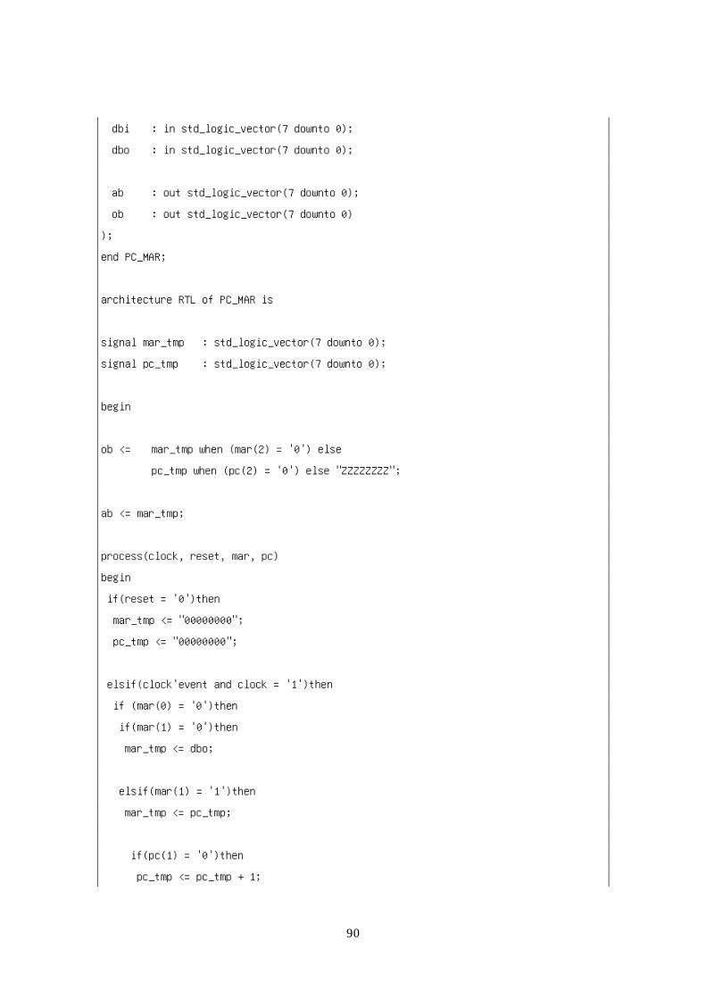
----- PC_MAR -----
library IEEE;
use IEEE.std_logic_1164.all;
use IEEE.std_logic_unsigned.all;
entity PC_MAR is
port(
clock : in std_logic;
reset : in std_logic;
mar : in std_logic_vector(4 downto 0);
pc : in std_logic_vector(2 downto 0);
90
dbi : in std_logic_vector(7 downto 0);
dbo : in std_logic_vector(7 downto 0);
ab : out std_logic_vector(7 downto 0);
ob : out std_logic_vector(7 downto 0)
);
end PC_MAR;
architecture RTL of PC_MAR is
signal mar_tmp : std_logic_vector(7 downto 0);
signal pc_tmp : std_logic_vector(7 downto 0);
begin
ob <= mar_tmp when (mar(2) = '0') else
pc_tmp when (pc(2) = '0') else "ZZZZZZZZ";
ab <= mar_tmp;
process(clock, reset, mar, pc)
begin
if(reset = '0')then
mar_tmp <= "00000000";
pc_tmp <= "00000000";
elsif(clock'event and clock = '1')then
if (mar(0) = '0')then
if(mar(1) = '0')then
mar_tmp <= dbo;
elsif(mar(1) = '1')then
mar_tmp <= pc_tmp;
if(pc(1) = '0')then
pc_tmp <= pc_tmp + 1;
91
end if;
end if;
elsif (mar(3) = '0') then
mar_tmp <= (mar_tmp) + 1;
elsif (mar(4) = '0') then
mar_tmp <= (mar_tmp) - 1;
elsif(pc(0) = '0')then
pc_tmp <= dbi;
end if;
end if;
end process;
end RTL;
付録 2-7:SYNCRONIZER の記述
----- SYNCRONIZER -----
library IEEE;
use IEEE.std_logic_1164.all;
use IEEE.std_logic_unsigned.all;
entity SYNCRONIZER is
port(
clock : in std_logic;
reset : in std_logic;
sp : in std_logic;
si : in std_logic;
ss : in std_logic;
set : in std_logic;
adr_inc : in std_logic;
92
adr_dec : in std_logic;
spsync : out std_logic;
sisync : out std_logic;
sssync : out std_logic;
setsync : out std_logic;
adr_inc_sync : out std_logic;
adr_dec_sync : out std_logic
);
end SYNCRONIZER;
architecture RTL of SYNCRONIZER is
signal sp_tmp1, si_tmp1, ss_tmp1, set_tmp1, adr_inc_tmp1, adr_dec_tmp1 : std_logic;
begin
process(clock,reset)
begin
if(reset = '0')then
sp_tmp1 <= '0';
si_tmp1 <= '0';
ss_tmp1 <= '0';
set_tmp1 <= '0';
adr_inc_tmp1 <= '0';
adr_dec_tmp1 <= '0';
spsync <= '0';
sisync <= '0';
sssync <= '0';
setsync <= '0';
adr_inc_sync <= '0';
adr_dec_sync <= '0';
elsif(clock'event and clock = '1')then
sp_tmp1 <= not(sp);
93
spsync <= not(sp) and (not(sp_tmp1));
si_tmp1 <= not(si);
sisync <= not(si) and (not(si_tmp1));
ss_tmp1 <= not(ss);
sssync <= not(ss) and (not(ss_tmp1));
set_tmp1 <= not(set);
setsync <= not(set) and (not(set_tmp1));
adr_inc_tmp1 <= not(adr_inc);
adr_inc_sync <= not(adr_inc) and (not(adr_inc_tmp1));
adr_dec_tmp1 <= not(adr_dec);
adr_dec_sync <= not(adr_dec) and (not(adr_dec_tmp1)
end if;
end process;
end RTL;
付録 2-8:IMEM の記述
RAM の記述はアルテラ社の Quartus II Web Edition ver4.2のウィザードに従って設計したので、VHDLの記述は割愛する。 ----IMEM----
library IEEE;
use IEEE.std_logic_1164.all;
entity IMEM is
port(
clock : in std_logic;
imem : in std_logic_vector(2 downto 0);
abi : in std_logic_vector(8 downto 0);
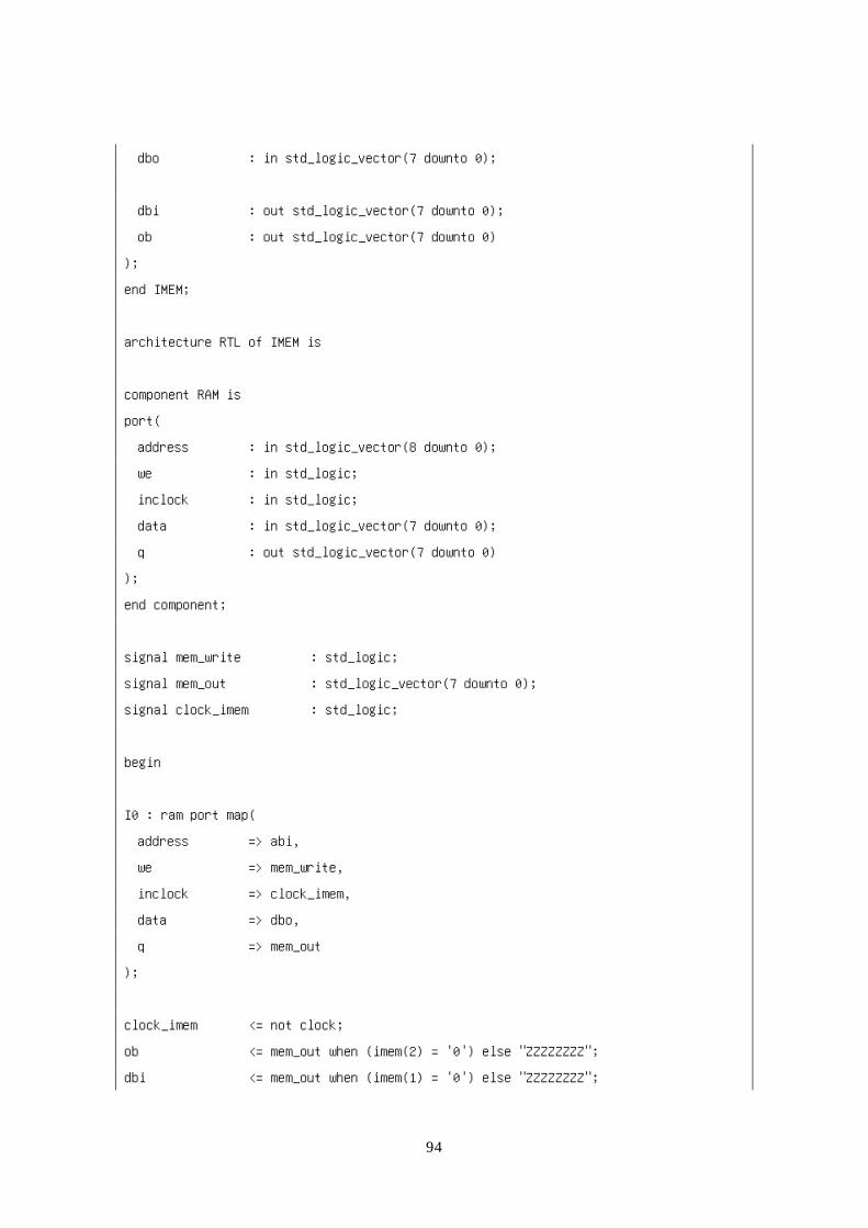
94
dbo : in std_logic_vector(7 downto 0);
dbi : out std_logic_vector(7 downto 0);
ob : out std_logic_vector(7 downto 0)
);
end IMEM;
architecture RTL of IMEM is
component RAM is
port(
address : in std_logic_vector(8 downto 0);
we : in std_logic;
inclock : in std_logic;
data : in std_logic_vector(7 downto 0);
q : out std_logic_vector(7 downto 0)
);
end component;
signal mem_write : std_logic;
signal mem_out : std_logic_vector(7 downto 0);
signal clock_imem : std_logic;
begin
I0 : ram port map(
address => abi,
we => mem_write,
inclock => clock_imem,
data => dbo,
q => mem_out
);
clock_imem <= not clock;
ob <= mem_out when (imem(2) = '0') else "ZZZZZZZZ";
dbi <= mem_out when (imem(1) = '0') else "ZZZZZZZZ";
95
mem_write <= not imem(0);
end RTL;
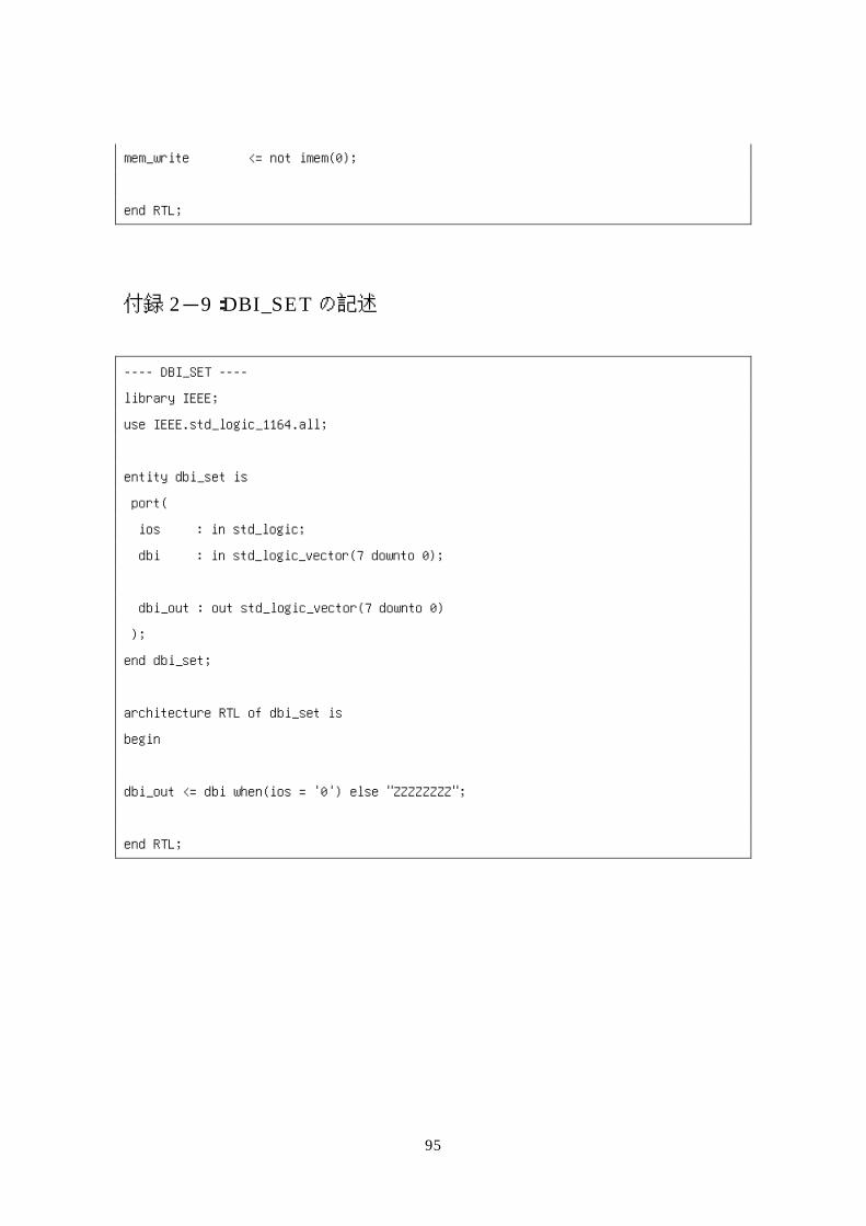
付録 2-9:DBI_SET の記述
---- DBI_SET ----
library IEEE;
use IEEE.std_logic_1164.all;
entity dbi_set is
port(
ios : in std_logic;
dbi : in std_logic_vector(7 downto 0);
dbi_out : out std_logic_vector(7 downto 0)
);
end dbi_set;
architecture RTL of dbi_set is
begin
dbi_out <= dbi when(ios = '0') else "ZZZZZZZZ";
end RTL;
96
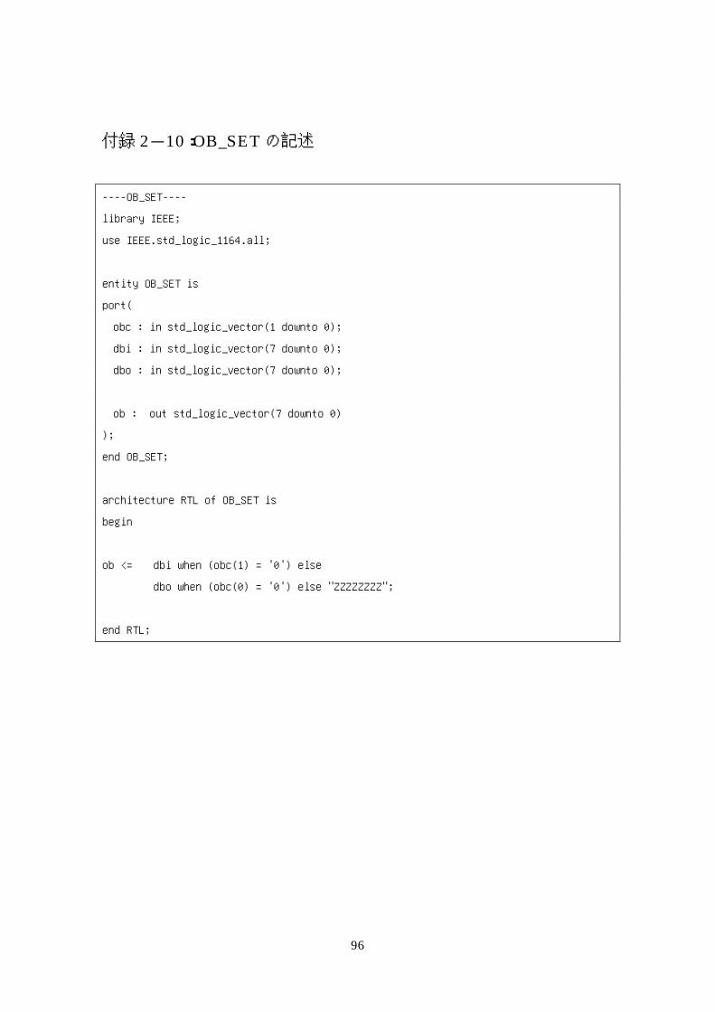
付録 2-10:OB_SET の記述
----OB_SET----
library IEEE;
use IEEE.std_logic_1164.all;
entity OB_SET is
port(
obc : in std_logic_vector(1 downto 0);
dbi : in std_logic_vector(7 downto 0);
dbo : in std_logic_vector(7 downto 0);
ob : out std_logic_vector(7 downto 0)
);
end OB_SET;
architecture RTL of OB_SET is
begin
ob <= dbi when (obc(1) = '0') else
dbo when (obc(0) = '0') else "ZZZZZZZZ";
end RTL;
![KL5C80A12命令説明書userweb.alles.or.jp/chunichidenko/nd80kl86setumeisyo/kl5...1 [KL5C8012の命令について] KL5C8012はZ80の命令を全く同じように実行するのですが、命令を実行するキルチキ数が異なっています。たとえば](https://img.pdfslide.tips/doc/110x75/5e4894425e9daf363f4aee0a/kl5c80a12e-1-kl5c8012-kl5c8012z80oeeoeoeeoeffoec.jpg)


![Z80命令説明書Z80命令説明書userweb.alles.or.jp/chunichidenko/nd3setumeisyo/nd3_z80...1 Z80命令説明書 [はじめに] Z80はザイログ社が開発した8ビットCPUで、8080(インテル社)の命令の全てを含み、さらにその上全く新しい多くの命令を実行](https://img.pdfslide.tips/doc/110x75/5e2a926c08e1b36d51021776/z80ez80e-1-z80e-z80fcoeec8ffffcpu8080ifffcieoe.jpg)

![まえがき - TIJ.co.jp[label] BLDD src, dst BLDD命命令は令は令は、、srcとdstでで示示示されされされるる2つのパつのパのパラララメーメーメータをタをタをもももってってっていいいますますます。。BLDD命命令を令を令を](https://img.pdfslide.tips/doc/110x75/60dc52e49aa2ff531e05490f/oe-tijcojp-label-bldd-src-dst-blddsrcdstcccoeoeoe2ffffffffffffbldd.jpg)