Embed Size (px)
Citation preview

SEOUL | Oct.7, 2016
안철오 박사 (메타리버테크놀러지), Oct. 7, 2016
디스플레이 및 반도체 산업에서 CUDA기술의 응용

2
AGENDA
Company overview
Semiconductor and Display
Thin film deposition process
Electro-Magnetic analysis
Particle-based plasma simulation

3
Linux Cluster (2002~2006)

4
Supercomputer (2007~2008)

5
GPU computing (2008~)
We met Dr. David Kirk
Mar. 11, 2008
at Yonsei University.

6
METARIVER TECHNOLOGY
company Metariver Technology Co., Ltd.
http://www.metariver.kr
address B-801, Garden 5 Works, 52, Chungmin-ro,
Songpa-gu, Seoul, 138-961, Korea
establishment 07/08/2009
business area GPU application software
Particle based multi-physics solver
product
samadii/dem (Discrete Element Method)
samadii/sciv (DSMC, Direct Simulation Monte Carlo)
samadii/em (Electro-Magnetic Simulation)
samadii/plasma (Particle-based plasma simulation)
samadii/lbm (CFD, Lattice Boltzmann Method)

7
TECHNOLOGY MAP
GPU Computing CUDA Technology
Fast Algorithm S/W Acceleration
HPC Technology Supercomputing
samadii/dem Discrete Element Method
samadii/sciv Direct Simulation Monte Carlo
samadii/plasma
Particle-based Plasma simulation
samadii/lbm CFD, Lattice Boltzmann Method
samadii/em Electro-Magnetic Solver

8

9

10
PARTICLE-BASED SIMULATION
• Lagrangian
• Explicit
• Very small time step
• Lots of iterations
• Length scale of particle
• The number of particles (N)
• Sufficient computing performance
• Rendering load

11
SEMICONDUCTOR AND DISPLAY

12
SEMICONDUCTOR Semiconductor production process
10/11/2016
ⒸIntel
Ion implantation (이온주입)
Lithography (노광)
Deposition (증착)
Ashing (애슁)
Etching (식각)

13
DISPLAY PANEL TFT(Thin Film Transistor) production process
10/11/2016
Lithography (노광)
Deposition (증착)
Cleasning (세정)
Etching (식각)
Develop (현상)
TFT processing Glass formation Color filter
processing
Cell and Module
assembly
ⒸCambridge Univ. Press Fabrication steps for TOS TFTs

14
SEMICONDUCTOR VS. DISPLAY PANEL Comparison of the structures
Ⓒsamsung
Schematic structure of (a) semiconductor (b) TFT(display panel)
(a) (b)
Ion implantation Lithography Deposition Ashing Etching
Lithography Deposition Cleansning Etching Develop

15
DEPOSITION
• 물질을 gas형태로 만들어 원하는 표면에 일정 두께로 막을 성형하는 과정 • PVD(Physical Vapor Deposition), APCVD(Atmospheric Pressure Chemical Vapor Deposition),
LPCVD(Low-Pressure CVD), PECVD(Plasma-Enhanced CVD), Sputtering(DC, RF, Magnetron etc.)
crucible
nozzles
target

16
ION IMPLANTATION
www2.austin.cc.tx.us/HongXiao/Book.htm
Introduction to Semiconductor
Manufacturing Technology, HongXiao,Ph.D.
Ion
Source Vacuum
Pump
Analyzer Magnet
Beam Line
End Analyzer
Wafers
Plasma Flooding System
Post Acceleration
Electrode
Extraction
Electrode
Suppression Electrode
Ion beam in
Ion beam out
B-field
Analyzer Magnet
• 이온을 다른 고체 물질에 주입 • 물리화학적 특성을 개질하거나 결정 구조를 변경하기 위한 목적

17
ETCHING AND ASHING Plasma applications
• Plasma Etching 회로패턴을 형성하기 위해 특정부분의 막을 선택적으로 제거
• Plasma Ashing 경화층 제거 및 유기물/오염물질 제거 (화공약품을 사용하는 습식 세정방식 대체)
Gabriel I. Font-Rodriguez, Cornell University
Plasma Etch Reactor Plasma Etching
http://www.plasmaetch.com/
Oxygen plasma (Asher)

18
THIN FILM DEPOSITION PROCESS
19
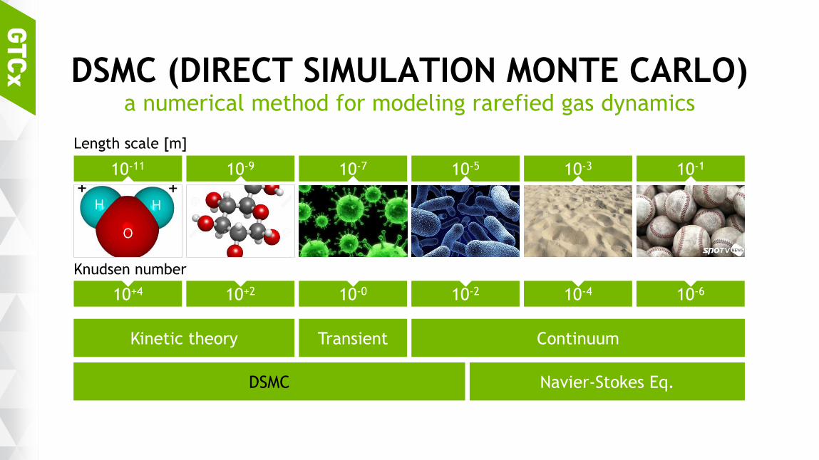
DSMC (DIRECT SIMULATION MONTE CARLO)
Length scale [m]
a numerical method for modeling rarefied gas dynamics
10-11 10-9 10-7 10-5 10-3 10-1
Continuum Transient Kinetic theory
10+4 10+2 10-0 10-2 10-4 10-6
Knudsen number
DSMC Navier-Stokes Eq.

20
RAREFIED GAS
ATMOSPHERE RAREFIED GAS

21
DSMC PARTICLE
The DSMC method models fluid flows using particles which represent a large number of real
molecules.
maximum collision number :
FN : 1011~1015
FN

22
CELL LINKED-LIST Thrust::sort_by_key
10/11/2016
3
6
7
8
9
10
11
12 13
14 16
17 0 6 7 8
3 5
0 1 2
4
2 5
15 4
1
Cell-id
(Hash value)
Particle-id
Thrust::sort_by_key
7 4 4 5 5 4 0 3 2 1 1 6 7 8 2 4 0 6
1 0 2 3 4 5 6 7 8 9 10 11 12 13 14 15 16 17
Cell-id
(Hash value)
Particle-id
7 4 4 5 5 4 0 3 2 1 1 6 7 8 2 4 0 6
16 6 9 10 8 14 7 1 2 5 15 3 4 11 17 12 0 13

23
SAMPLE CODE
/// 각 입자의 소속 cell주소 pAddrCllp[i].x=floor(( px[i].x - cllpmin.x)* _1cllpsz); pAddrCllp[i].y=floor(( px[i].y - cllpmin.y)* _1cllpsz); pAddrCllp[i].z=floor(( px[i].z - cllpmin.z)* _1cllpsz); /// 각 입자의 hash value phash[i]= pAddrCllp[i].z * cllpN.x * cllpN.y + pAddrCllp[i].y * cllpN.x + pAddrCllp[i].x;

24
SAMPLE CODE
thrust::device_ptr<uint> th_phash(phash); thrust::device_ptr<uint> th_pid(pid); /// phash를 기준으로 particle을 sorting thrust::sort_by_key(th_phash, th_phash+Nb, th_pid, thrust::less<int>()); pid=thrust::raw_pointer_cast(th_pid); phash=thrust::raw_pointer_cast(th_phash);

25
COLLISION
• HS(Hard Sphere)
• VHS(Variable Hard Sphere) Model
Collision cross-section
• Dissociation reaction
• Recombination reaction
• Exchange reaction
AB + T → A + B + T
AB + T ← A + B + T
AB + CD ↔ AC + BD
Chemical reaction
• Elastic collision
• In-elastic collision
- Translation–Rotational Exchange model
- Translation–Vibration Exchange model
Collision
A’ A

26
BOUNDARY CONDITIONS
• Evaporation inlet
: Maxwell-Boltzmann distribution
: cosine distribution
: evaporation temperature
• Particle inlet
• Pressure inlet
Inlet boundary conditions
• Wall
: diffusion rate
: adsorption rate
: wall temperature effect
• Particle outlet
• Pressure outlet
• TMP-outlet
Outlet boundary conditions

27
Maxwell-Boltzmann distribution Cosine distribution
PARTICLE DISTRIBUTIONS
1000 2000 3000 4000
Pro
babilit
y d
ensi
ty
: 500K
: 700K
: 1800K
0 0
0.0005
0.001
0.005
0.2
0.4
0.6
0.8
1.0
1.2
Probability density
: N=0
: N=1
: N=2

28
DEPOSITION RATE TEST #1 Cosine distribution (N)
N=5 N=3 N=1
Single point source

29
DEPOSITION RATE TEST #2 Nozzle length
L=10mm
L=20mm
L=30mm
L=40mm
depth
nozzle length
nozzle length
depth

30
DEPOSITION RATE TEST #3 Nozzle angle
60º 45º 30º 10º 0º -10º -30º -45º
Rate of deposition according to angle
angle
Linear source

31

32

33
ELECTRO-MAGNETIC ANALYSIS

34
.
Magnetic field induced current of coil Electric field induced current of coil Electric wave propagation
Generalized Electro-Magnetic Solver

35
GOVERNING EQUATIONS Maxwell’s Equations
( Faraday’s law )
( Ampere’s law )
( Gauss’s law )
( Gauss’s law-magnetic )
tE
Et
EH
t
BE
B
Er
0
0
( Current conservation )
Magnetostatics Electrostatics Quasi-statics Electric current
Electric wave Electric current (Frequency) Electrodynamics Magnetic wave

36
PARTICLE-BASED PLASMA SIMULATION

37
PARTICLE-BASED PLASMA SIMULATION samadii/plasma
이온과 전자의 충돌에 의한
plasma 반응해석*
전자기장에서
전자와 이온의 거동 해석
Plasma chamber내부
전자기장 해석 이온과 전자 수밀도에 의한
국부적 전자기장 해석

38
PARTICLE-BASED PLASMA SIMULATION

39
PIC (PARTICLE-IN-CELL)
1
0
43
2
0Q 1Q
2Q3Q
4Q
5Q
1
2
3 4
00E
1E
2E
3E
4E
i
j
iV
q
d
j
iN
Q
VE
QV
2
BVEqF ii

40

41
PARTICLE-BASED PLASMA SIMULATION samadii/sciv + samadii/em
Number density Electric potential Electric field
-300V 0V
-2.00e+13
0.00e+0
2.00e+13
4.00e+13
6.00e+13
0 0.06 0.12 0.18 0.24 0.3
Z [m]
Number density
-300V 0V -300V 0V -300V 0V
electron 9.11e-30 [kg]
ion 6.63e-26 [kg] (1:7300)

42
www2.austin.cc.tx.us/HongXiao/Book.htm
Introduction to Semiconductor
Manufacturing Technology, HongXiao,Ph.D.
Ion
Source Vacuum
Pump
Analyzer Magnet
Beam Line
End Analyzer
Wafers
Plasma Flooding System
Post Acceleration
Electrode
Extraction
Electrode
Suppression Electrode
Ion beam in
Ion beam out
B-field
Analyzer Magnet
• 이온을 다른 고체 물질에 주입 • 물리화학적 특성을 개질하거나 결정 구조를 변경하기 위한 목적
Ion Implantation

43
source head
(high voltage)
manipulator
repeller plate
(**kV)
filament
(**kV+600V)
slit1 Slit3
(0V) slit2
(low voltage)
(-**kV)
slit1 Slit2
(low voltage)
(-**kV)
slit3
(0V)
FN : 1.00E+7[#] 이온(BFx+) 생성률 : 3.04E+17 [#/s]
전자 생성률 : 2.72E+17 [#/s]
(약 0.05 [A])
Time step : 2.02E-11[sec.]
N~7,845,600[EA]
Ion Implantation
ion
electron

44

45
RIE (Reactive Ion Etching) Chamber
f=13.56[MHz]
Time step : 0.292[ns] (2.92E-10)
pump-out
(4-side)
chamber
(ground)
wafer
shower head
V0=30[V], V=V0cos(ωt)
H~150
ion electron

46

SEOUL | Oct.7, 2016
THANK YOU


![반도체 디스플레이 - imgstock.naver.comimgstock.naver.com/upload/research/industry/1421020659640.pdf · ... TCL UHD TV [그림 2] Hisense UHD TV ... 과거 LCD와 PDP의 경합](https://img.pdfslide.tips/doc/110x75/5ab67ecd7f8b9ab7638dbc9e/-tcl-uhd-tv-2-hisense-uhd-tv-.jpg)