Embed Size (px)
Citation preview

hm90560-cm44-10107-4e-corr-x1-05.doc 1 / 25
Corrections of Hardware Manual
MB90560/5 -
hm90560-cm44-10107-4e-corr-x1-05
© Fujitsu Microelectronics Europe GmbH
Addendum, MB90560/5 Hardware Manual (CM42-10107-4E) This is the Addendum for the Hardware Manual CM42-10107-4E of the MB90560/5 microcontroller series. It describes all known discrepancies of the MB90560/5 microcontroller series Hardware Manual.
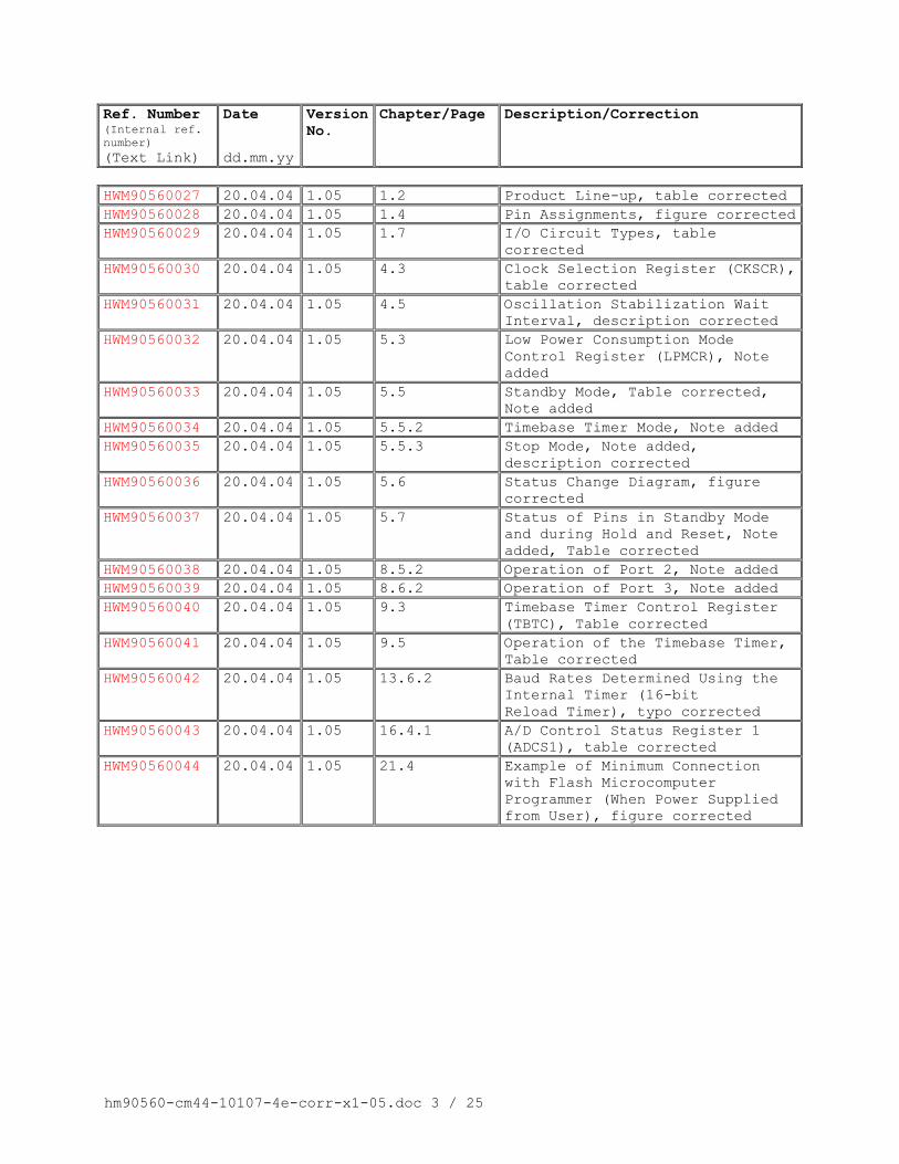
Ref. Number (Internal ref. number)
Date Version No.
Chapter/Page Description/Correction
(Text Link) dd.mm.yy

hm90560-cm44-10107-4e-corr-x1-05.doc 2 / 25
Ref. Number (Internal ref. number)
Date Version No.
Chapter/Page Description/Correction
(Text Link) dd.mm.yy
HWM90560001
11.06.01 1.00 6.4.5 Interrupt Processing time
HWM90560002
11.06.01 1.00 1.8 Power On Reset
HWM90560003
20.08.01 1.02 19 Flash Security Feature, Description updated
HWM90560004
11.06.01 1.00 1.8 Handling the Device, Information about reserved memory area
HWM90560005
28.06.01 1.01 1.8 RTO Port behaviour during Reset
HWM90560006 28.01.02 1.03 1.2 Product Lineup, typos corrected HWM90560007 28.01.02 1.03 1.4 Pin Assignment, description addedHWM90560008 28.01.02 1.03 1.7 I/O circuit types, description
added HWM90560009 28.01.02 1.03 1.8 Handling the devices, description
of PLL operation added HWM90560010 28.01.02 1.03 2.3 Memory Maps, address range
corrected HWM90560011 28.01.02 1.03 4.4 Clock mode, description added HWM90560012 28.01.02 1.03 5.1 Low Power Consumption Mode,
typo corrected HWM90560013 28.01.02 1.03 5.5.1 Sleep mode, description removed HWM90560014 28.01.02 1.03 5.8 Usage Notes on Low Power
Consumption Mode, description added
HWM90560015 28.01.02 1.03 12.3.2 Output Compare Registers, Note added
HWM90560016 28.01.02 1.03 12.4.2 Output Compare, Note added HWM90560017 28.01.02 1.03 13.1 Overview of UART, baud rate
description corrected HWM90560018 28.01.02 1.03 13.2 Configuration of UART,
description corrected (Reload Timer)
HWM90560019 28.01.02 1.03 13.4.2 Mode Register (SMR0/SMR1), description corrected (Reload Timer)
HWM90560020 28.01.02 1.03 13.6 UART Baud Rates, description corrected (Reload Timer)
HWM90560021 28.01.02 1.03 13.7.1 UART, start bit detection description added
HWM90560022 28.01.02 1.03 14.4 DTP/External interrupt circuit, Typo corrected
HWM90560023 28.01.02 1.03 19 512K-Bit (64 KB) Flash Memory, Typo corrected
HWM90560024 28.01.02 1.03 19.3 Flash Control Status Register (FMCS), Bit setting corrected
HWM90560025 30.08.02 1.04 1.8 Pin output state in standby mode HWM90560026 30.08.02 1.04 4.5 PLL clock oscillation
stabilization wait time
hm90560-cm44-10107-4e-corr-x1-05.doc 3 / 25
Ref. Number (Internal ref. number)
Date Version No.
Chapter/Page Description/Correction
(Text Link) dd.mm.yy
HWM90560027 20.04.04 1.05 1.2 Product Line-up, table corrected HWM90560028 20.04.04 1.05 1.4 Pin Assignments, figure correctedHWM90560029 20.04.04 1.05 1.7 I/O Circuit Types, table
corrected HWM90560030 20.04.04 1.05 4.3 Clock Selection Register (CKSCR),
table corrected HWM90560031 20.04.04 1.05 4.5 Oscillation Stabilization Wait
Interval, description corrected HWM90560032 20.04.04 1.05 5.3 Low Power Consumption Mode
Control Register (LPMCR), Note added
HWM90560033 20.04.04 1.05 5.5 Standby Mode, Table corrected, Note added
HWM90560034 20.04.04 1.05 5.5.2 Timebase Timer Mode, Note added HWM90560035 20.04.04 1.05 5.5.3 Stop Mode, Note added,
description corrected HWM90560036 20.04.04 1.05 5.6 Status Change Diagram, figure
corrected HWM90560037 20.04.04 1.05 5.7 Status of Pins in Standby Mode
and during Hold and Reset, Note added, Table corrected
HWM90560038 20.04.04 1.05 8.5.2 Operation of Port 2, Note added HWM90560039 20.04.04 1.05 8.6.2 Operation of Port 3, Note added HWM90560040 20.04.04 1.05 9.3 Timebase Timer Control Register
(TBTC), Table corrected HWM90560041 20.04.04 1.05 9.5 Operation of the Timebase Timer,
Table corrected HWM90560042 20.04.04 1.05 13.6.2 Baud Rates Determined Using the
Internal Timer (16-bit Reload Timer), typo corrected
HWM90560043 20.04.04 1.05 16.4.1 A/D Control Status Register 1 (ADCS1), table corrected
HWM90560044 20.04.04 1.05 21.4 Example of Minimum Connection with Flash Microcomputer Programmer (When Power Supplied from User), figure corrected

hm90560-cm44-10107-4e-corr-x1-05.doc 4 / 25
HWM90560001
Chapter 6.4.5 Interrupt processing Time The correct interrupt processing time is calculated with: When returning from an interrupt : o = 15 + 6 * z machine cycles
HWM90560002
Power-On Reset ===================================
Output “unknown value” , when the power supply Is turned on If F2MC-16LX is used. (Note)
1.Device covered MB90V560, MB90F562, MB90F568, MB90561, MB90562, MB90567, MB90568
2. Note: During testing it has been found that some port pins may enter an undefined state during power on. By asserting RSTx during the power on reset (217 cycles of main clock) port pins can be forced to high impedance. The following Ports will output a High Impedance (Hi-z) at the terminal when the power supply is turned on when PONR and RSTX = 1:
P40 – P67 The following ports will output High Impedance (High-Z) on RSTX or with the End of PONR and Start of internal clocks:
P00 – P17 The following Ports will output High Impedance (high-Z) with the End of PONR and Start of the internal Clock. RSTX does not force the pins to high-Z during power on.
P20 – P37
Note: This workaround will work for Mode pin setting 011 (Single chip, Internal ROM external bus), 110 (Burn_In ROM), 111 (EPROM mode)

hm90560-cm44-10107-4e-corr-x1-05.doc 5 / 25
The following diagram shows the timing chart in detail.
Under “power-on reset” 217 x oscillation clock frequency (8.192ms in case of oscillation clock frequency = 16MHz)
Waiting time to be stabilized oscillation 218 x oscillation clock frequency (16.384ms in case of oscillation clock frequency = 16MHz).
Vcc (power supply i
“power-on ”i
RSTX (external h )sign
lRST (
Internal
MCLK (main clock) i l
Internal operation
Output port 0 1
How to “Hi-”d
“power-on ”
RSTX (external h )sign
lOutput port 0 1
Timing h
Under “power-on ”Oscillation
outpu“unknown l
”Hi-
PrograExecuti
Hi-
Input external 2 x oscillation clock f

hm90560-cm44-10107-4e-corr-x1-05.doc 6 / 25
HWM90560003
CHAPTER 19 512K-BIT (64 KB) FLASH MEMORY
Flash Security Feature ==================== Correction: The Flash Security Feature is not inside MB90F562 Series, these Feature is only inside MB90F562B Series!
Chapter 19.8 Flash Security Feature
The Flash security Controller provides possibilities to protect the content of the flash memory from being read from external pins.
• Flash Security Feature One predefined address of the flash memory is assigned to the Flash Security Controller (512K-bit flash memory: FF0001). If the protection code of "01H" is written is this address, access to the flash memory is restricted. Once the flash memory is protected, performing the chip erase operation only can unlock the function otherwise read/write access to the flash memory from any external pins is not generally possible. This function is suitable for applications requiring security of self-containing and data stored in the flash memory. If the target application requires any part of program to locate outside the microcontroller, the Flash Security Controller can not offer the intended features. For this reason, the External Vector Fetch mode should not be used when the protection code is set. Programming of the flash microcontroller by standard parallel programmer may require unique set-up. For example, with the programmer from Minato Electronics the device checking should be turned off. Writing the protection code is generally recommended to take place at the end of the flash programming. This is to avoid unnecessary protection during the programming. In order to re-program the once protected flash memory, the chip erase operation should be performed. For further information, please contact Fujitsu.
HWM90560004
Chapter 1.8 Handling the Device Reserved Area ================================= Last Word of Memory (FFFFFE – FFFFFF) is reserved AREA. Do not use this last WORD.

hm90560-cm44-10107-4e-corr-x1-05.doc 7 / 25
HWM90560005
Chapter 1.8 Handling the device RTO Port pin (P30-P35) behaviour during Reset When using RTO port Function or the port pins P30-P35, the following behaviour occurs if the external RST Reset pin is asserted: When asserting RST low, the RTO Ports (P30-P35) will drive active ‘High’ Level about 400 ns, starting with the falling edge of the RST signal. This might cause problems in some kind of applications. Especially in case of IGBT drivers, a workaround could be used to disable the output drivers during reset. This could be done e.g by using an additional I/O port, which is tristate during RST. With a corresonding pull-up/down resistance at this port, the level on this pin can be hold high/low during reset in order to keep the driver disabled. After the reset the drivers could be enabled by initialising the port pin correspondingly by software.
HWM90560006
Chapter 1.2 Product Lineup Typo in the table title: Old: Table 1.2-1 Product Lineup of the MB90560/565 Series New: Table 1.2-1 Product Lineup of the MB90560 Series Typo in the Table: MODEL DESCRIPTION: Old:
Model MB90V560 MB90F562/B MB90562/A MB90561/A
Package QFP-64 (FPT-64P-M09: 0.65 mm pin pitch) QFP-64 (FPT-64P-M06: 1.00 mm pin pitch) SH-DIP (DIP-64P-M01: 1.778 mm pin pitch)
Correction:
Model MB90V560 MB90F562/B MB90562/A MB90561/A
Package QFP-64 (FPT-64P-M09: 0.65 mm pin pitch) QFP-64 (FPT-64P-M06: 1.00 mm pin pitch) SH-DIP-64 (DIP-64P-M01: 1.778 mm pin pitch)

hm90560-cm44-10107-4e-corr-x1-05.doc 8 / 25
HWM90560007
Chapter 1.4 Pin Assignments Missing Note added Figure 1.4-3 Pin Assignment of DIP-64P-M01 *1: Neither MB90568, MB90567 nor MB90F568 are supported.
HWM90560008
Chapter 1.7 I/O Circuit Types Table 1.7-1: Description added Classification Circuit type Remarks
A • Oscillation circuit Oscillation feedback resistor: 1 MΩ approx.
E • CMOS I/O pin • :• :• IOL = 12mA
HWM90560009
Chapter 1.8 Notes on Handling Devices Following Note is added: o Notes on during operation of PLL clock mode
If the PLL clock mode is selected, the microcontroller attempt to be working with the self-oscillating circuit even when there is no external oscillator or external clock input is stopped. Performance of this operation, however, cannot be guaranteed.
HWM90560010
Chapter 2.3 Memory Maps Incorrect Address range for MB90V560 mentioned Correction:
Model Address #1 Address #2 Address #3 MB90V560 FE0000H * 004000H * 001100H

hm90560-cm44-10107-4e-corr-x1-05.doc 9 / 25
HWM90560011
Chapter 4.4 Clock Mode Clock Mode Transition Description added Note:
…In attempting to switch the clock mode, do not attempt to switch to another clock mode or low-power consumption mode until the first switching is completed. The MCM bit of the clock selection register (CKSCR) indicates that switching is completed.
HWM90560012
Chapter 5.1 Low Power Consumption Mode Correction of Description Standby mode Old: Note: Because stop mode and hardware standby mode turn the oscillation clock off, these modes save the most power while data is being retained. Because the MB90560/565 series does not have a pin for the hardware standby function, the stop mode cannot be used. New: Note: Because stop mode and hardware standby mode turn the oscillation clock off, these modes save the most power while data is being retained. In attempting to switch the clock mode, do not attempt to switch to another clock mode or low-power consumption mode until the first switching is completed. The MCM bit of the clock selection register (CKSCR) indicates that switching is completed.
HWM90560013
Chapter 5.5.1 Sleep Mode Description of ‘Hold Function’ is invalid. The entry will be removed with next version. Hold function In sleep mode, the hold function is enabled. A hold request sets the hold status.

hm90560-cm44-10107-4e-corr-x1-05.doc 10 / 25
HWM90560014
Chapter 5.8 Usage Notes on Low Power Consumption Mode Description added at the end of the text. Switching the clock mode In attempting to switch the clock mode, do not attempt to switch to another clock mode or low-power consumption mode until the first switching is completed. The MCM bit of the clock selection register (CKSCR) indicates that switching is completed. The following description was added below the " Switching to Standby Mode and Interrupts": Notes on the transition to standby mode To set a pin to high impedance when the pin is shared by a peripheral function and a port in stop mode or time-base timer mode, use the following procedure: 1. Disable the output of peripheral functions. 2. Set the SPL bit of the low-power consumption mode control register (LPMCR) to 1, and set the STP bit to 1 or set the TMD bit to 0.
The description of " PLL clock oscillation stabilization wait interval" was corrected as follows: In main clock mode, the PLL multiplication circuit stops. When changing to PLL clock mode, it is necessary to reserve the PLL clock oscillation stabilization wait interval. While waiting for PLL clock oscillation stabilization, the CPU operates on the main clock. The PLL clock oscillation stabilization wait interval is fixed at 214/HCLK (HCLK: clock oscillation frequency). In PLL stop mode, the main clock and PLL multiplication circuit stop. At return from PLL stop mode, it is necessary to allot the main clock oscillation stabilization wait interval and PLL clock oscillation stabilization wait interval. The oscillation stabilization wait intervals for the main clock and PLL clock are counted simultaneously according to the value specified in the oscillation stabilization wait interval selection bits (CKSCR: WS1, WS0) in the clock selection register. The oscillation stabilization wait interval selection bits (CKSCR: WS1, WS0) in the clock selection register must be selected accordingly to account for the longer of main clock and PLL clock oscillation stabilization wait interval. The PLL clock oscillation stabilization wait interval, however, requires 214/HCLK or more. Set the oscillation stabilization wait interval selection bits (CKSCR: WS1, WS0) in the clock selection register to "10B" or "11B".
HWM90560015
Chapter 12.3.2 Output Compare Registers Following note is added after the text: Note: To rewriting the compare register, within the compare interrupt routine or compare operation is disabled.

hm90560-cm44-10107-4e-corr-x1-05.doc 11 / 25
Be sure not to occur simultaneously a compare match and writing the compare register.
HWM90560016
Chapter 12.4.2 Output Compare Output Compare Timing: Following sentence is invalid and will be removed with next version: No compare operation with the counter value is performed when setting the compare register. Figure 12.4-7 ‘Compare Operation during Replacement of Compare Register’ is invalid and will be removed with next version. Following Note is added after Figure 12.4-9: Note: To rewriting the compare register, within the compare interrupt routine or compare operation is disabled. Be sure not to occur simultaneously a compare match and writing the compare register.
HWM90560017
Chapter 13.1 Overview of UART Table 13.1-1 UART Functions Correction of Baud Rate description
Function
Baud rate • Up to 2MHz (when the machine clock is operated at 16MHz) • A dedicated baud rate generator is provided. • Baud rate by an external clock (clock input through the
SCK0/SCK1 pins) • Internal clock (internal clocks supplied from 16-bit reload
timer 0 and 1 can be used.) • The baud rate can be selected from a total of eight types
hm90560-cm44-10107-4e-corr-x1-05.doc 12 / 25
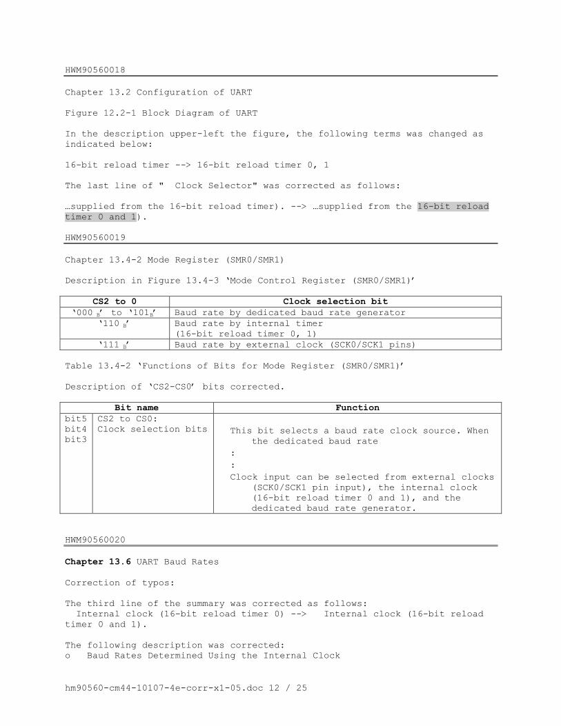
HWM90560018
Chapter 13.2 Configuration of UART Figure 12.2-1 Block Diagram of UART In the description upper-left the figure, the following terms was changed as indicated below: 16-bit reload timer --> 16-bit reload timer 0, 1 The last line of " Clock Selector" was corrected as follows: …supplied from the 16-bit reload timer). --> …supplied from the 16-bit reload timer 0 and 1). HWM90560019
Chapter 13.4-2 Mode Register (SMR0/SMR1) Description in Figure 13.4-3 ‘Mode Control Register (SMR0/SMR1)’
CS2 to 0 Clock selection bit ‘000 B’ to ‘101B’ Baud rate by dedicated baud rate generator
‘110 B’ Baud rate by internal timer (16-bit reload timer 0, 1)
‘111 B’ Baud rate by external clock (SCK0/SCK1 pins)
Table 13.4-2 ‘Functions of Bits for Mode Register (SMR0/SMR1)’ Description of ‘CS2-CS0’ bits corrected.
Bit name Function bit5bit4bit3
CS2 to CS0: Clock selection bits
• This bit selects a baud rate clock source. When
the dedicated baud rate • :• :• Clock input can be selected from external clocks
(SCK0/SCK1 pin input), the internal clock (16-bit reload timer 0 and 1), and the dedicated baud rate generator.
HWM90560020
Chapter 13.6 UART Baud Rates Correction of typos: The third line of the summary was corrected as follows: Internal clock (16-bit reload timer 0) --> Internal clock (16-bit reload timer 0 and 1). The following description was corrected: o Baud Rates Determined Using the Internal Clock
hm90560-cm44-10107-4e-corr-x1-05.doc 13 / 25
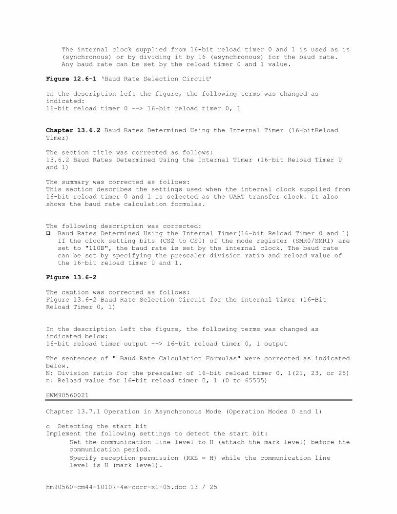
The internal clock supplied from 16-bit reload timer 0 and 1 is used as is (synchronous) or by dividing it by 16 (asynchronous) for the baud rate. Any baud rate can be set by the reload timer 0 and 1 value.
Figure 12.6-1 ‘Baud Rate Selection Circuit’ In the description left the figure, the following terms was changed as indicated: 16-bit reload timer 0 --> 16-bit reload timer 0, 1
Chapter 13.6.2 Baud Rates Determined Using the Internal Timer (16-bitReload Timer) The section title was corrected as follows: 13.6.2 Baud Rates Determined Using the Internal Timer (16-bit Reload Timer 0 and 1) The summary was corrected as follows: This section describes the settings used when the internal clock supplied from 16-bit reload timer 0 and 1 is selected as the UART transfer clock. It also shows the baud rate calculation formulas.
The following description was corrected: Baud Rates Determined Using the Internal Timer(16-bit Reload Timer 0 and 1)
If the clock setting bits (CS2 to CS0) of the mode register (SMR0/SMR1) are set to "110B", the baud rate is set by the internal clock. The baud rate can be set by specifying the prescaler division ratio and reload value of the 16-bit reload timer 0 and 1.
Figure 13.6-2 The caption was corrected as follows: Figure 13.6-2 Baud Rate Selection Circuit for the Internal Timer (16-Bit Reload Timer 0, 1)
In the description left the figure, the following terms was changed as indicated below: 16-bit reload timer output --> 16-bit reload timer 0, 1 output The sentences of " Baud Rate Calculation Formulas" were corrected as indicated below. N: Division ratio for the prescaler of 16-bit reload timer 0, 1(21, 23, or 25) n: Reload value for 16-bit reload timer 0, 1 (0 to 65535) HWM90560021
Chapter 13.7.1 Operation in Asynchronous Mode (Operation Modes 0 and 1) o Detecting the start bit Implement the following settings to detect the start bit:
• Set the communication line level to H (attach the mark level) before the communication period.
• Specify reception permission (RXE = H) while the communication line level is H (mark level).

hm90560-cm44-10107-4e-corr-x1-05.doc 14 / 25
• Do not specify reception permission (RXE = H) for periods other than the communication period (without mark level). Otherwise, data is not received correctly.
• After the stop bit is detected (the RDRF flag is set to 1), specify reception inhibition (RXE = L) while the communication line level is H (mark level).
Note that specifying reception permission at the timing shown below obstructs the correct recognition of the input data (SIN) by the microcontroller.
• Example of operation if reception permission (RXE = H) is specified while the communication line level is L.
HWM90560022
Chapter 14.4 DTP/External interrupt circuit Table 14.4-1 Note below table corrected

hm90560-cm44-10107-4e-corr-x1-05.doc 15 / 25
Note: A read-modify-write instruction always reads "1" from the DTP/interrupt cause register (EIRR). If more than one external interrupt request output is enabled (EN7 to EN0 of ENIR are set to 1), clear to 0 only the bit for which the CPU accepted an interrupt (any of bits ER7 to ER0 that are set to 1). Do not clear the other bits without a valid reason. HWM90560023
Chapter 19 512K-Bit (64 KB) Flash Memory Chapter 19.1 Overview of the 512K-Bit Memory Correction: Characteristics of the 512K-Bit Flash Memory
Minimum of 10,000 write/erase operations
HWM90560024
Chapter 19.3 Flash Control Status Register (FMCS) Typo corrected in table 19.3-1
Bit name Function
bit3 bit1
Reserved: Reserved bit
• Always set this bit to "0".
HWM90560025
Pin output state in standby mode • Details The following problem has been found for all products in MB90560/565 Series for some pins serving as a resource output and general-purpose port: when a transition is made to a standby mode (stop mode or time-base timer mode) with the resource output enabled, the pins are not placed in the Hi-Z state although the pin state setting pin is Hi-Z (SPL bit = 1). When a transition is made to a standby mode with the following states established, the pins shown in the table below are not placed in the Hi-Z state and they remain in the resource output state. State setting: Resource output enabled SPL bit = 1 (Port state is Hi-Z setting is standby mode) Products Pins not placed in Hi-Z state in standby mode MB90V560, MB90F562/B,
P21/TO0, P23/TO1, P30/RTO0, P31/RTO1, P32/RTO2, P33/RTO3, P34/RTO4, P35/RTO5, P37/SOT0

hm90560-cm44-10107-4e-corr-x1-05.doc 16 / 25
MB90561/A, MB90562/A, MB90F568, MB90567, MB90568
• Solution To place the above pins in the Hi-Z state in the standby mode, the pins must be set by software to general-purpose input ports as follows before transitioning to a standby mode.
(1) Set “input” using the port data direction register (DDR) for the shared general-purpose port.
(2) Disable the resource output. (3) Transition to the standby mode.
HWM90560026
PLL clock oscillation stabilization wait time • Details An oscillation stabilization wait time of 214/HCLK or more must be set at the following state transition: PLL stop mode → PLL clock mode This setting is not described in the hardware manuals. At the above state transitions, the PLL clock oscillation stabilization wait time is not counted automatically by hardware. Consequently, set 215/HCLK (10 b) or 217/HCLK (11 b) for the oscillation stabilization wait time selection bits (WS: 1 bit, WS: 0 bit) of the clock selection register (CKSCR). Note that a malfunction may occur if the following transitions are made when 214/HCLK or more is not set as the oscillation stabilization wait time. Also, at the transition from the main clock mode to the PLL clock mode, the oscillation stabilization wait time is 214/HCLK irrespective of the oscillation stabilization wait time setting of the clock selection register (CKSCR).
HWM90560027
Chapter 1.2 Product Lineup The caption was corrected as follows: Table 1.2-1 Product Lineup of the MB90560 Series

hm90560-cm44-10107-4e-corr-x1-05.doc 17 / 25
HWM90560028
Chapter 1.4 Pin Assignments The following description was added at the under-left of Figure 1.4-3: *1: Neither MB90568, MB90567 nor MB90F568 are supported. HWM90560029
Chapter 1.7 I/O Circuit Types
HWM90560030
Chapter 4.3 Clock Selection Register (CKSCR) The shading in the table below indicates changes made to Table 4.3-1.
Bit name Function
bit13 bit12
WS1, WS0: Oscillation Stabilization wait interval selection bit
• These bits select the oscillation stabilization wait interval for the oscillation clock after the stop mode has been cleared due to an external interrupt. When PLL stop mode is returned to PLL clock mode, the oscillation stabilization wait interval requires 214/HCLK or more. When changing to PLL clock mode, these bits are set to "10B" or "11 B". …
bit10 MCS: :

hm90560-cm44-10107-4e-corr-x1-05.doc 18 / 25
Machine clock selection bit
• When the main clock mode is switched to PLL clock mode, the oscillation stabilization wait interval is fixed to 214/HCLK. The oscillation stabilization wait interval is about 4.1 ms if the oscillation clock frequency is 4 MHz.) • When the main clock has been selected, the oscillation clock divided by 2 is used as the machine clock. :
HWM90560031
Chapter 4.5 Oscillation Stabilization Wait Interval The last line of " Oscillation Stabilization Wait Interval" was corrected as indicated by the shading below. … during an oscillation stabilization wait interval. After the oscillation stabilization wait interval has elapsed, the CPU changes to PLL clock mode.
HWM90560032
Chapter 5.3 Low Power Consumption Mode Control Register (LPMCR) The following note was added at the end of the page: Note: To set a pin to high impedance when the pin is shared by a peripheral function and a port in stop mode or time-base timer mode, disable the output of peripheral functions, and set the STP bit of the low-power consumption mode control register (LPMCR) to 1 or set the TMD bit to 0. This applies to the following pins: P21/TO0, P23/TO1, P30/RTO0, P31/RTO1, P32/RTO2, P33/RTO3, P34/RTO4, P35/RTO5, P37/SOT0
HWM90560033
Chapter 5.5 Standby Mode
The following note was added to " Operating Status during Standby Mode": Note: To set a pin to high impedance when the pin is shared by a peripheral function and a port in stop mode or time-base timer mode, disable the output of peripheral functions, and set the STP bit of the low-power consumption mode control register (LPMCR) to 1 or set the TMD bit to 0.

hm90560-cm44-10107-4e-corr-x1-05.doc 19 / 25
This applies to the following pins: P21/TO0, P23/TO1, P30/RTO0, P31/RTO1, P32/RTO2, P33/RTO3, P34/RTO4, P35/RTO5, P37/SOT0
HWM90560034
Chapter 5.5.2 Timebase Timer Mode The following note was added to " Switching to Timebase Timer Mode": Note: To set a pin to high impedance when the pin is shared by a peripheral function and a port in time-base timer mode, disable the output of peripheral functions, and set the TMD bit of the low-power consumption mode control register (LPMCR) to 0. This applies to the following pins: P21/TO0, P23/TO1, P30/RTO0, P31/RTO1, P32/RTO2, P33/RTO3, P34/RTO4, P35/RTO5, P37/SOT0
HWM90560035
Chapter 5.5.3 Stop Mode The following note was added to " Switching to Stop Mode": Note: To set a pin to high impedance when the pin is shared by a peripheral function and a port in stop mode, disable the output of peripheral functions, and set the STP bit of the low-power consumption mode control register (LPMCR) to 1. This applies to the following pins: P21/TO0, P23/TO1, P30/RTO0, P31/RTO1, P32/RTO2, P33/RTO3, P34/RTO4, P35/RTO5, P37/SOT0
The following sentence was added at the second line of " Release of Stop Mode": At return from stop mode, since the oscillation clock (HCLK) has stopped, the stop mode is released after the oscillation stabilization wait interval of the main clock.
The following note was added at the end of the page: Note: In PLL stop mode, the main clock and PLL multiplication circuit stop. At return from PLL stop mode, it is necessary to allot the main clock oscillation stabilization wait interval and PLL clock oscillation stabilization wait interval. The oscillation stabilization wait intervals for the main clock and PLL clock are counted simultaneously according to the value specified in the oscillation stabilization wait interval selection bits (CKSCR: WS1, WS0) in the clock selection register. The oscillation stabilization wait interval selection bits (CKSCR: WS1, WS0) in the clock selection register must be selected accordingly to account for the longer of main clock and PLL clock oscillation stabilization wait interval. The PLL clock oscillation stabilization wait interval, however, requires 214/HCLK or more. Set the

hm90560-cm44-10107-4e-corr-x1-05.doc 20 / 25
oscillation stabilization wait interval selection bits (CKSCR: WS1, WS0) in the clock selection register to "10B" or "11B".

hm90560-cm44-10107-4e-corr-x1-05.doc 21 / 25
HWM90560036
Chapter 5.6 Status Change Diagram
HWM90560037
Chapter 5.7 Status of Pins in Standby Mode and during Hold and Reset The following note was added to " Status of Pins in Single-Chip Mode": Note: To set a pin to high impedance when the pin is shared by a peripheral function and a port in stop mode or time-base timer mode, disable the output of peripheral functions, and set the STP bit of the low-power consumption mode control register (LPMCR) to 1 or set the TMD bit to 0. This applies to the following pins: P21/TO0, P23/TO1, P30/RTO0, P31/RTO1, P32/RTO2, P33/RTO3, P34/RTO4, P35/RTO5, P37/SOT0

hm90560-cm44-10107-4e-corr-x1-05.doc 22 / 25
HWM90560038
Chapter 8.5.2 Operation of Port 2 The following note was added to " Port operation in stop or time-base timer mode": Note: To set a pin to high impedance when the pin is shared by a peripheral function and a port in stop mode or time-base timer mode, disable the output of peripheral functions, and set the STP bit of the low-power consumption mode control register (LPMCR) to 1 or set the TMD bit to 0. This applies to the following pins: P21/TO0, P23/TO1
HWM90560039
Chapter 8.6.2 Operation of Port 3 The following note was added to " Port operation in stop or time-base timer mode": Note: To set a pin to high impedance when the pin is shared by a peripheral function and a port in stop mode or time-base timer mode, disable the output of peripheral functions, and set the STP bit of the low-power consumption mode control register (LPMCR) to 1 or set the TMD bit to 0. This applies to the following pins: P30/RTO0, P31/RTO1, P32/RTO2, P33/RTO3, P34/RTO4, P35/RTO5, P37/SOT0
hm90560-cm44-10107-4e-corr-x1-05.doc 23 / 25
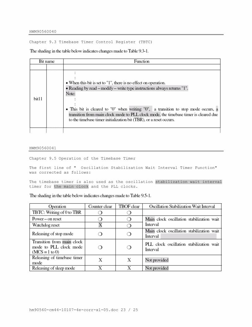
HWM90560040
Chapter 9.3 Timebase Timer Control Register (TBTC)
HWM90560041
Chapter 9.5 Operation of the Timebase Timer The first line of " Oscillation Stabilization Wait Interval Timer Function" was corrected as follows: The timebase timer is also used as the oscillation stabilization wait interval timer for the main clock and the PLL clocks.

hm90560-cm44-10107-4e-corr-x1-05.doc 24 / 25
HWM90560042
Chapter 13.6.2 Baud Rates Determined Using the Internal Timer (16-bit Reload Timer) The footer of the Table 13.6-4 was corrected as follows: N: Division ratio for the prescaler of 16-bit reload timer 0, 1
HWM90560043
Chapter 16.4.1 A/D Control Status Register 1 (ADCS1)

hm90560-cm44-10107-4e-corr-x1-05.doc 25 / 25
HWM90560044
Chapter 21.4 Example of Minimum Connection with Flash Microcomputer Programmer (When Power Supplied from User)


![Chapter 12(20131111) [호환 모드]contents.kocw.net/KOCW/document/2014/sungkyunkwan/kimcheolhwan2/14.pdf☞경제급전문제는다음과같이기술할수있음 식(12.4.2) 로주어진등식제약조건(equality](https://img.pdfslide.tips/doc/110x75/5e278c6f74ccc973ae28d2c5/chapter-1220131111-eeoe-aeoeeeoeeeoeeeeoe.jpg)


![Descargar publicación [1.03 MB]](https://img.pdfslide.tips/doc/110x75/58a01f361a28ab746f8b5522/descargar-publicacion-103-mb.jpg)
