Embed Size (px)
Citation preview

27 Via Porto Grande, Rancho Palos Verdes, CA, 90275. Ph. # 1-310-377-6029. Fax # 1-310-377-9940.
Rev.: 1, January 2010. ASNT6123 1
A d v a n c e d S c i e n c e a n d N o v e l T e c h n o l o g y
A D S A N T E C
ASNT6123 25Gbps Dual Transimpedance Amplifier
• Two parallel broadband transimpedance amplifiers for low noise receiver side applications.
• Both amplifiers feature automatic input offset control and a peak detector.
• Independently adjustable 16-20GHz of analog bandwidth per amplifier channel.
• 80.0dBΩ of transimpedance differential gain per amplifier.
• 15.0pA/sqrtHz of input referred noise density (0.1 to 20GHz) for each amplifier.
• Two CML output interfaces with 50Ω termination and 300mVp-p single-ended swing.
• Single +3.3V power supply.
• Power consumption: 460mW.
• Exhibits low jitter and limited temperature variation over industrial temperature range.
• Fabricated in SiGe for high performance, yield, and reliability.
DESCRIPTION
Functional Block Diagram
1
PD BIAS
BIASBIAS
TIA BUF1 EF OBUF
AOC
BUF2 EF
PD
TIA BUF1 EF OBUF
AOC
BUF2 EF
PD
TIA BUF1 EF OBUF
AOC
BUF2 EF
PD
TIA BUF1 EF OBUF
AOC
BUF2 EF
PD
TIA BUF1 EF OBUF
AOC
BUF2 EF
PD
TIA BUF1 EF OBUF
AOC
BUF2 EF
PD
TIA BUF1 EF OBUF
AOC
BUF2 EF
PD
TIA BUF1 EF OBUF
AOC
BUF2 EF
PD
TIA BUF1 EF OBUF
AOC
BUF2 EF
PD
TIA BUF1 EF OBUF
AOC
BUF2 EF
PD
TIA BUF1 EF OBUF
AOC
BUF2 EF
PD
TIA BUF1 EF OBUF
AOC
BUF2 EF
PD
TIA BUF1 EFEF OBUF
AOC
BUF2BUF2 EFEF
PD
TIA BUF1 EF OBUF
AOC
BUF2 EF
PD
TIA BUF1 EF OBUF
AOC
BUF2 EF
PD
TIA BUF1 EF OBUF
AOC
BUF2 EF
PD
TIA BUF1 EF OBUF
AOC
BUF2 EF
PD
TIA BUF1 EF OBUF
AOC
BUF2 EF
PD
TIA BUF1 EF OBUF
AOC
BUF2 EF
PD
TIA BUF1 EF OBUF
AOC
BUF2 EF
PD
TIA BUF1 EF OBUF
AOC
BUF2 EF
PD
TIA BUF1 EF OBUF
AOC
BUF2 EF
PD
TIA BUF1 EF OBUF
AOC
BUF2 EF
PD
TIA BUF1 EF OBUF
AOC
BUF2 EF
PD
TIA BUF1 EF OBUF
AOC
BUF2 EF
PD
TIA BUF1 EFEF OBUF
AOC
BUF2BUF2 EFEF
PDPD BIAS
PKADJ_1PKADJ_1
PKADJ_2
BW CONTROL
27 Via Porto Grande, Rancho Palos Verdes, CA, 90275. Ph. # 1-310-377-6029. Fax # 1-310-377-9940.
Rev.: 1, January 2010. ASNT6123 2
A d v a n c e d S c i e n c e a n d N o v e l T e c h n o l o g y
A D S A N T E C
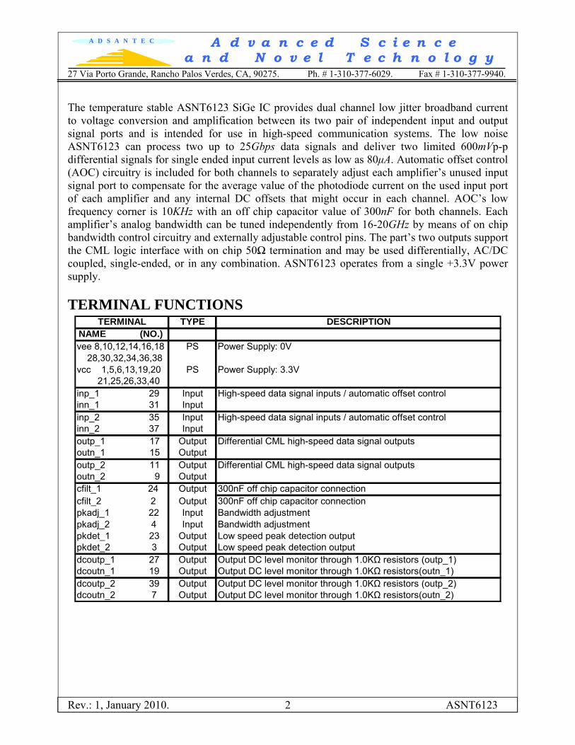
The temperature stable ASNT6123 SiGe IC provides dual channel low jitter broadband current to voltage conversion and amplification between its two pair of independent input and output signal ports and is intended for use in high-speed communication systems. The low noise ASNT6123 can process two up to 25Gbps data signals and deliver two limited 600mVp-p differential signals for single ended input current levels as low as 80μA. Automatic offset control (AOC) circuitry is included for both channels to separately adjust each amplifier’s unused input signal port to compensate for the average value of the photodiode current on the used input port of each amplifier and any internal DC offsets that might occur in each channel. AOC’s low frequency corner is 10KHz with an off chip capacitor value of 300nF for both channels. Each amplifier’s analog bandwidth can be tuned independently from 16-20GHz by means of on chip bandwidth control circuitry and externally adjustable control pins. The part’s two outputs support the CML logic interface with on chip 50Ω termination and may be used differentially, AC/DC coupled, single-ended, or in any combination. ASNT6123 operates from a single +3.3V power supply. TERMINAL FUNCTIONS
TERMINAL TYPE DESCRIPTIONNAME (NO.) vee 8,10,12,14,16,18 PS Power Supply: 0V 28,30,32,34,36,38vcc 1,5,6,13,19,20 PS Power Supply: 3.3V 21,25,26,33,40inp_1 29 Input High-speed data signal inputs / automatic offset controlinn_1 31 Inputinp_2 35 Input High-speed data signal inputs / automatic offset controlinn_2 37 Inputoutp_1 17 Output Differential CML high-speed data signal outputsoutn_1 15 Outputoutp_2 11 Output Differential CML high-speed data signal outputsoutn_2 9 Outputcfilt_1 24 Output 300nF off chip capacitor connectioncfilt_2 2 Output 300nF off chip capacitor connectionpkadj_1 22 Input Bandwidth adjustmentpkadj_2 4 Input Bandwidth adjustmentpkdet_1 23 Output Low speed peak detection outputpkdet_2 3 Output Low speed peak detection outputdcoutp_1 27 Output Output DC level monitor through 1.0KΩ resistors (outp_1)dcoutn_1 19 Output Output DC level monitor through 1.0KΩ resistors(outn_1)dcoutp_2 39 Output Output DC level monitor through 1.0KΩ resistors (outp_2)dcoutn_2 7 Output Output DC level monitor through 1.0KΩ resistors(outn_2)
27 Via Porto Grande, Rancho Palos Verdes, CA, 90275. Ph. # 1-310-377-6029. Fax # 1-310-377-9940.
Rev.: 1, January 2010. ASNT6123 3
A d v a n c e d S c i e n c e a n d N o v e l T e c h n o l o g y
A D S A N T E C
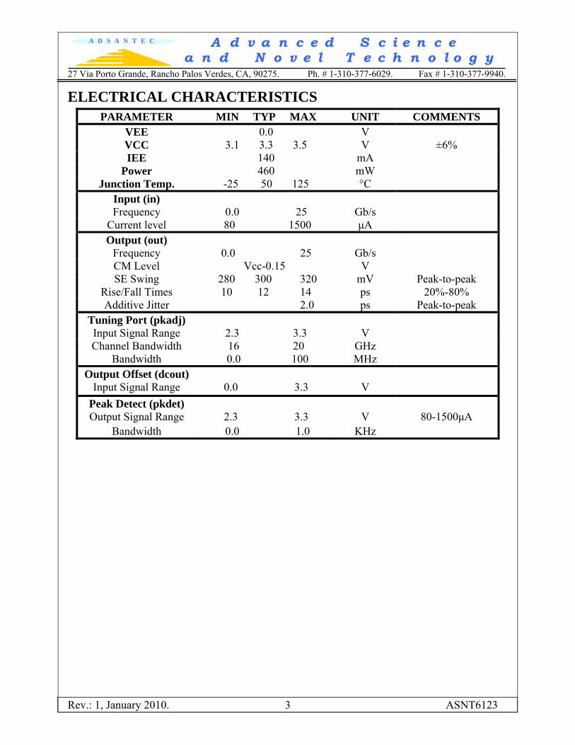
ELECTRICAL CHARACTERISTICS PARAMETER MIN TYP MAX UNIT COMMENTS
VEE 0.0 V VCC 3.1 3.3 3.5 V ±6% IEE 140 mA
Power 460 mW Junction Temp. -25 50 125 °C
Input (in) Frequency
0.0 25
Gb/s
Current level 80 1500 μA Output (out)
Frequency
0.0 25
Gb/s
CM Level Vcc-0.15 V SE Swing 280 300 320 mV Peak-to-peak
Rise/Fall Times 10 12 14 ps 20%-80% Additive Jitter 2.0 ps Peak-to-peak
Tuning Port (pkadj) Input Signal Range
2.3 3.3
V
Channel Bandwidth 16 20 GHz Bandwidth 0.0 100 MHz
Output Offset (dcout) Input Signal Range
0.0 3.3
V
Peak Detect (pkdet) Output Signal Range
2.3 3.3
V
80-1500μA
Bandwidth 0.0 1.0 KHz