Embed Size (px)
Citation preview
A 6.5-μV/°C Offset Drift Compensation
Technique for Dynamic Comparator
Daiki Tabira and Kenichi Ohhata Department of Electrical and Electronics Engineering, Kagoshima University, Kagoshima, Japan
Email:[email protected]
Abstract—The offset drift of a dynamic comparator was
analyzed using a simple model in order to clarify the offset
drift mechanism. We found that it was possible to nullify the
offset drift component due to size variability by controlling
the gate common voltage (Vcom). We conducted experiments
to validate our estimations by using a test chip fabricated in
180-nm CMOS technology. Consequently, we found that the
amount of variability of VTH and W/L could be extracted
from the measured offset voltage. Moreover, the offset drift
was reduced to 6.5 μV/°C by controlling the temperature
dependence of Vcom.
Index Terms—offset drift, comparator, analog-to-digital
converter, CMOS analog circuits
I. INTRODUCTION
Digital calibration has attracted a great deal of
attention as a power reduction technique for analog-to-
digital converters (ADCs) [1]−[5]. This technique
drastically reduces the power of the comparator because
it compensates for the offset voltage of the comparator;
therefore, no preamplifier is required, and the comparator
can be composed of small MOS transistors.
Digital calibration is divided broadly into two
categories, that is, background and foreground calibration.
In background calibration, the calibration is performed in
every cycle. For example, the ADC of Chung et al. [5]
performs the conversion operation in the first half of the
cycle and the calibration in the second half. The
comparator dissipates relatively large power in this ADC
because the comparator needs to operate twice in a cycle.
The ADC of Figueiredo et al. [2] has two fine ADCs that
alternately repeat calibration and conversion; however,
this ADC requires a large chip area.
In the foreground calibration, calibration is performed
intermittently. This is generally done in the power-on
sequence. Once the calibration is performed, the
comparator operates in the normal mode; thereby, the
issue of background calibration is solved. However, it is
known that the offset voltage increases when the
temperature changes after the calibration. The effective
number of bits (ENOB) is reported to change by ±0.15 bit
in a 6-bit ADC when the temperature varies in the range
of 125°C after the calibration [1]. This suggests that the
foreground calibration is effective in the case of 6-bit
Manuscript received January 23, 2013; revised March 13, 2013.
resolution; however, it generates unacceptable error in the
case of 8-or-more-bit resolution.
The mechanism of the offset drift on the temperature
change was analyzed using a simple model then a drift
compensation technique was proposed. Moreover, the
feasibility of the offset drift model and the effectiveness
of the drift compensation technique were verified using a
test chip fabricated in 180-nm CMOS technology.
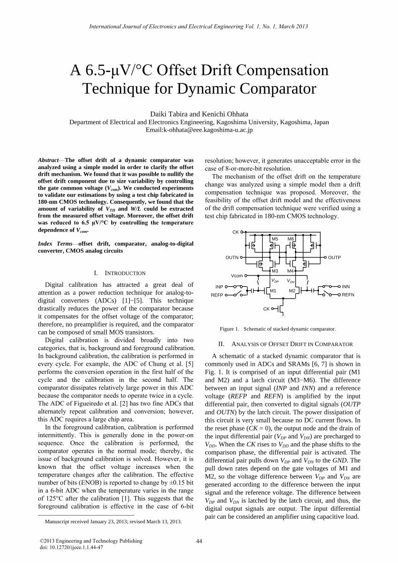
Figure 1. Schematic of stacked dynamic comparator.
II. ANALYSIS OF OFFSET DRIFT IN COMPARATOR
A schematic of a stacked dynamic comparator that is
commonly used in ADCs and SRAMs [6, 7] is shown in
Fig. 1. It is comprised of an input differential pair (M1
and M2) and a latch circuit (M3−M6). The difference
between an input signal (INP and INN) and a reference
voltage (REFP and REFN) is amplified by the input
differential pair, then converted to digital signals (OUTP
and OUTN) by the latch circuit. The power dissipation of
this circuit is very small because no DC current flows. In
the reset phase (CK = 0), the output node and the drain of
the input differential pair (VDP and VDN) are precharged to
VDD. When the CK rises to VDD and the phase shifts to the
comparison phase, the differential pair is activated. The
differential pair pulls down VDP and VDN to the GND. The
pull down rates depend on the gate voltages of M1 and
M2, so the voltage difference between VDP and VDN are
generated according to the difference between the input
signal and the reference voltage. The difference between
VDP and VDN is latched by the latch circuit, and thus, the
digital output signals are output. The input differential
pair can be considered an amplifier using capacitive load.
M4
CK
INP INN
OUTN OUTP
CK
M1 M2
M3
M5 M6
Vcom
REFP REFN
VDP VDN
International Journal of Electronics and Electrical Engineering Vol. 1, No. 1, March 2013
44©2013 Engineering and Technology Publishing doi: 10.12720/ijeee.1.1.44-47
Figure 2. Equivalent circuit of amplifier.
An equivalent circuit of the amplifier is shown in Fig.
2, where CL is the parasitic capacitance at VDP and VDN,
and ID, gm and rd are the drain current, transconductance
and drain resistance, respectively. In this case, the gate
voltage of M2 is lower than that of M1 by ∆VIN. The latch
circuit is activated when the voltage of VDP reaches VDD −
VTH3; therefore, the voltage difference of ∆VD is generated.
Thus, the voltage gain of the amplifier is expressed as
DDD
mTH
DDDd
mTHd
VI
gV
VIr
gVrG
1
33 (1)
where λ is the channel length modulation coefficient. The
gain is about three to five for 180-nm CMOS technology.
Therefore, the offset voltage from the latch circuit is
small. The simulated offset voltage breakdown of the
stacked comparator is shown in Fig. 3. As expected from
the equivalent circuit, the offset contribution from the
latch circuit is negligible, and the offset of the differential
pair is dominant. Therefore, we made an offset drift
model focusing on the input differential pair.
Figure 3. Breakdown of simulated offset voltage.
Figure 4. Differential pair and considered mismatch.
Let us consider the situation shown in Fig. 4 in order to
analyze the offset voltage of the input differential pair
(M1 and M2). The various mismatches in M1 and M2
cause the offset voltage. We consider the mismatch of the
threshold voltage and the transistor size (W/L). Here, we
assume the drain current is expressed as
DSTHGSox
D VVVL
WCI
1
2, (2)
taking into consideration the velocity saturation and the
channel length modulation effect. The offset voltage of
this model is expressed as
LW
LWVVVV THcomTHoff
/
/ , (3)
where Vcom is the common gate voltage (see Fig. 1) that
determines VGS of M1 and M2. Therefore, the
temperature coefficient of the offset voltage is expressed
as
LW
LW
dT
dV
dT
dV
dT
Vd
dT
dVTHcomTHoff
/
/
. (4)
Equation (4) indicates that the dependence of the offset
on the temperature is determined by d∆VTH/dT and
(dVcom/dT − dVTH/dT) because ∆(W/L) is independent
from the temperature. The temperature coefficient of the
offset deviates randomly because ∆VTH and ∆(W/L)
deviate randomly. This means that the offset drift cannot
be compensated for collectively because the offset
voltage in each comparator has different temperature
dependence. However, if we design the temperature
coefficient as dVcom/dT = dVTH/dT, the 2nd term of (4) can
be nullified. In this case, the temperature coefficient can
be reduced to
dT
Vd
dT
dVTHoff
. (5)
III. EXPERIMENTAL RESULTS
With our model, the offset drift is determined by the
temperature dependence of ∆VTH, Vcom, and VTH.
Moreover, the offset drift can be reduced by appropriately
controlling the temperature dependence of Vcom. We
conducted some experiments in order to validate these
estimations using a test chip.
International Journal of Electronics and Electrical Engineering Vol. 1, No. 1, March 2013
45
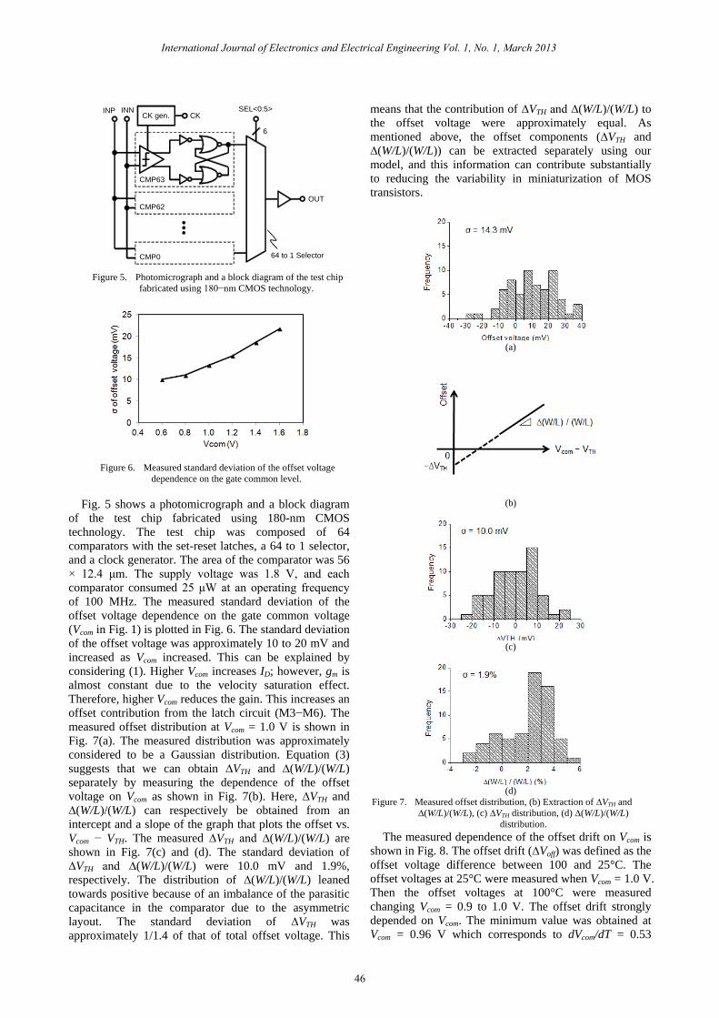
Figure 5. Photomicrograph and a block diagram of the test chip
fabricated using 180−nm CMOS technology.
Figure 6. Measured standard deviation of the offset voltage
dependence on the gate common level.
Fig. 5 shows a photomicrograph and a block diagram
of the test chip fabricated using 180-nm CMOS
technology. The test chip was composed of 64
comparators with the set-reset latches, a 64 to 1 selector,
and a clock generator. The area of the comparator was 56
× 12.4 μm. The supply voltage was 1.8 V, and each
comparator consumed 25 μW at an operating frequency
of 100 MHz. The measured standard deviation of the
offset voltage dependence on the gate common voltage
(Vcom in Fig. 1) is plotted in Fig. 6. The standard deviation
of the offset voltage was approximately 10 to 20 mV and
increased as Vcom increased. This can be explained by
considering (1). Higher Vcom increases ID; however, gm is
almost constant due to the velocity saturation effect.
Therefore, higher Vcom reduces the gain. This increases an
offset contribution from the latch circuit (M3−M6). The
measured offset distribution at Vcom = 1.0 V is shown in
Fig. 7(a). The measured distribution was approximately
considered to be a Gaussian distribution. Equation (3)
suggests that we can obtain ∆VTH and ∆(W/L)/(W/L)
separately by measuring the dependence of the offset
voltage on Vcom as shown in Fig. 7(b). Here, ∆VTH and
∆(W/L)/(W/L) can respectively be obtained from an
intercept and a slope of the graph that plots the offset vs.
Vcom − VTH. The measured ∆VTH and ∆(W/L)/(W/L) are
shown in Fig. 7(c) and (d). The standard deviation of
∆VTH and ∆(W/L)/(W/L) were 10.0 mV and 1.9%,
respectively. The distribution of ∆(W/L)/(W/L) leaned
towards positive because of an imbalance of the parasitic
capacitance in the comparator due to the asymmetric
layout. The standard deviation of ∆VTH was
approximately 1/1.4 of that of total offset voltage. This
means that the contribution of ∆VTH and ∆(W/L)/(W/L) to
the offset voltage were approximately equal. As
mentioned above, the offset components (∆VTH and
∆(W/L)/(W/L)) can be extracted separately using our
model, and this information can contribute substantially
to reducing the variability in miniaturization of MOS
transistors.
(a)
(b)
(c)
(d)
Figure 7. Measured offset distribution, (b) Extraction of ∆VTH and
∆(W/L)/(W/L), (c) ∆VTH distribution, (d) ∆(W/L)/(W/L)
distribution.
The measured dependence of the offset drift on Vcom is
shown in Fig. 8. The offset drift (∆Voff) was defined as the
offset voltage difference between 100 and 25°C. The
offset voltages at 25°C were measured when Vcom = 1.0 V.
Then the offset voltages at 100°C were measured
changing Vcom = 0.9 to 1.0 V. The offset drift strongly
depended on Vcom. The minimum value was obtained at
Vcom = 0.96 V which corresponds to dVcom/dT = 0.53
CMP63
CMP62
CMP0
INP INN SEL<0:5>
6
OUT
CK gen. CK
64 to 1 Selector
International Journal of Electronics and Electrical Engineering Vol. 1, No. 1, March 2013
46
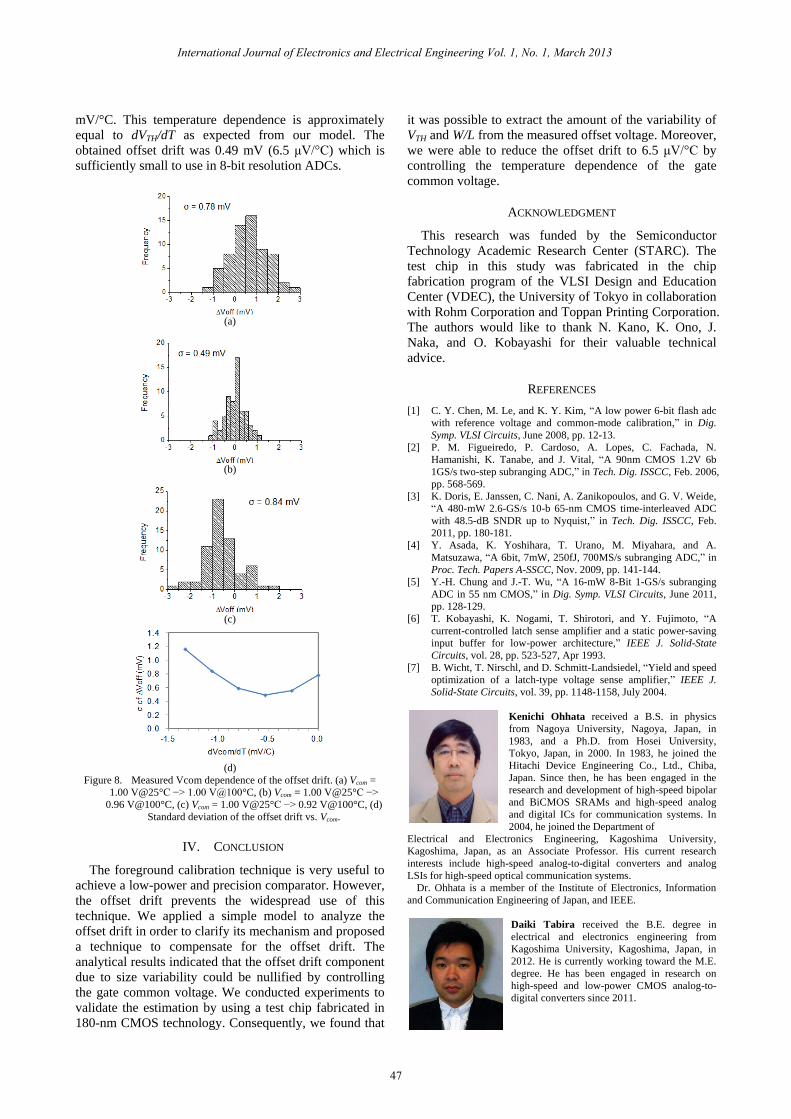
mV/°C. This temperature dependence is approximately
equal to dVTH/dT as expected from our model. The
obtained offset drift was 0.49 mV (6.5 μV/°C) which is
sufficiently small to use in 8-bit resolution ADCs.
(a)
(b)
(c)
(d)
Figure 8. Measured Vcom dependence of the offset drift. (a) Vcom =
1.00 V@25°C −> 1.00 V@100°C, (b) Vcom = 1.00 V@25°C −>
0.96 V@100°C, (c) Vcom = 1.00 V@25°C −> 0.92 V@100°C, (d)
Standard deviation of the offset drift vs. Vcom.
IV. CONCLUSION
The foreground calibration technique is very useful to
achieve a low-power and precision comparator. However,
the offset drift prevents the widespread use of this
technique. We applied a simple model to analyze the
offset drift in order to clarify its mechanism and proposed
a technique to compensate for the offset drift. The
analytical results indicated that the offset drift component
due to size variability could be nullified by controlling
the gate common voltage. We conducted experiments to
validate the estimation by using a test chip fabricated in
180-nm CMOS technology. Consequently, we found that
it was possible to extract the amount of the variability of
VTH and W/L from the measured offset voltage. Moreover,
we were able to reduce the offset drift to 6.5 μV/°C by
controlling the temperature dependence of the gate
common voltage.
ACKNOWLEDGMENT
This research was funded by the Semiconductor
Technology Academic Research Center (STARC). The
test chip in this study was fabricated in the chip
fabrication program of the VLSI Design and Education
Center (VDEC), the University of Tokyo in collaboration
with Rohm Corporation and Toppan Printing Corporation.
The authors would like to thank N. Kano, K. Ono, J.
Naka, and O. Kobayashi for their valuable technical
advice.
REFERENCES
[1] C. Y. Chen, M. Le, and K. Y. Kim, “A low power 6-bit flash adc
with reference voltage and common-mode calibration,” in Dig.
Symp. VLSI Circuits, June 2008, pp. 12-13.
[2] P. M. Figueiredo, P. Cardoso, A. Lopes, C. Fachada, N.
Hamanishi, K. Tanabe, and J. Vital, “A 90nm CMOS 1.2V 6b
1GS/s two-step subranging ADC,” in Tech. Dig. ISSCC, Feb. 2006,
pp. 568-569.
[3] K. Doris, E. Janssen, C. Nani, A. Zanikopoulos, and G. V. Weide,
“A 480-mW 2.6-GS/s 10-b 65-nm CMOS time-interleaved ADC
with 48.5-dB SNDR up to Nyquist,” in Tech. Dig. ISSCC, Feb.
2011, pp. 180-181.
[4] Y. Asada, K. Yoshihara, T. Urano, M. Miyahara, and A.
Matsuzawa, “A 6bit, 7mW, 250fJ, 700MS/s subranging ADC,” in
Proc. Tech. Papers A-SSCC, Nov. 2009, pp. 141-144.
[5] Y.-H. Chung and J.-T. Wu, “A 16-mW 8-Bit 1-GS/s subranging
ADC in 55 nm CMOS,” in Dig. Symp. VLSI Circuits, June 2011,
pp. 128-129.
[6] T. Kobayashi, K. Nogami, T. Shirotori, and Y. Fujimoto, “A
current-controlled latch sense amplifier and a static power-saving
input buffer for low-power architecture,” IEEE J. Solid-State
Circuits, vol. 28, pp. 523-527, Apr 1993.
[7] B. Wicht, T. Nirschl, and D. Schmitt-Landsiedel, “Yield and speed
optimization of a latch-type voltage sense amplifier,” IEEE J.
Solid-State Circuits, vol. 39, pp. 1148-1158, July 2004.
Kenichi Ohhata received a B.S. in physics
from Nagoya University, Nagoya, Japan, in
1983, and a Ph.D. from Hosei University,
Tokyo, Japan, in 2000. In 1983, he joined the
Hitachi Device Engineering Co., Ltd., Chiba,
Japan. Since then, he has been engaged in the
research and development of high-speed bipolar
and BiCMOS SRAMs and high-speed analog
and digital ICs for communication systems. In
2004, he joined the Department of
Electrical and Electronics Engineering, Kagoshima University,
Kagoshima, Japan, as an Associate Professor. His current research
interests include high-speed analog-to-digital converters and analog
LSIs for high-speed optical communication systems.
Dr. Ohhata is a member of the Institute of Electronics, Information
and Communication Engineering of Japan, and IEEE.
Daiki Tabira received the B.E. degree in
electrical and electronics engineering from
Kagoshima University, Kagoshima, Japan, in
2012. He is currently working toward the M.E.
degree. He has been engaged in research on
high-speed and low-power CMOS analog-to-
digital converters since 2011.
International Journal of Electronics and Electrical Engineering Vol. 1, No. 1, March 2013
47


![מ''עב ח''שגא לויכ תויגולונכט ערוזה א.ב.מ · 9 A T [0.1 µV to 200 mV] 14 μV/V 10 A T (200 mV to 1V] 6.7 μV/V 11 A T (1 V to 10 V] 5 μV/V 12 A T (10](https://img.pdfslide.tips/doc/110x75/5fe670d75e9e322d3f25ba0d/-oe-oe-9-a-t-01.jpg)