Embed Size (px)
Citation preview
8/9/2019 AIWA_BZG-2_SimpleSvcMnls-2
http://slidepdf.com/reader/full/aiwabzg-2simplesvcmnls-2 1/29
CD-R/RW MECHANISM
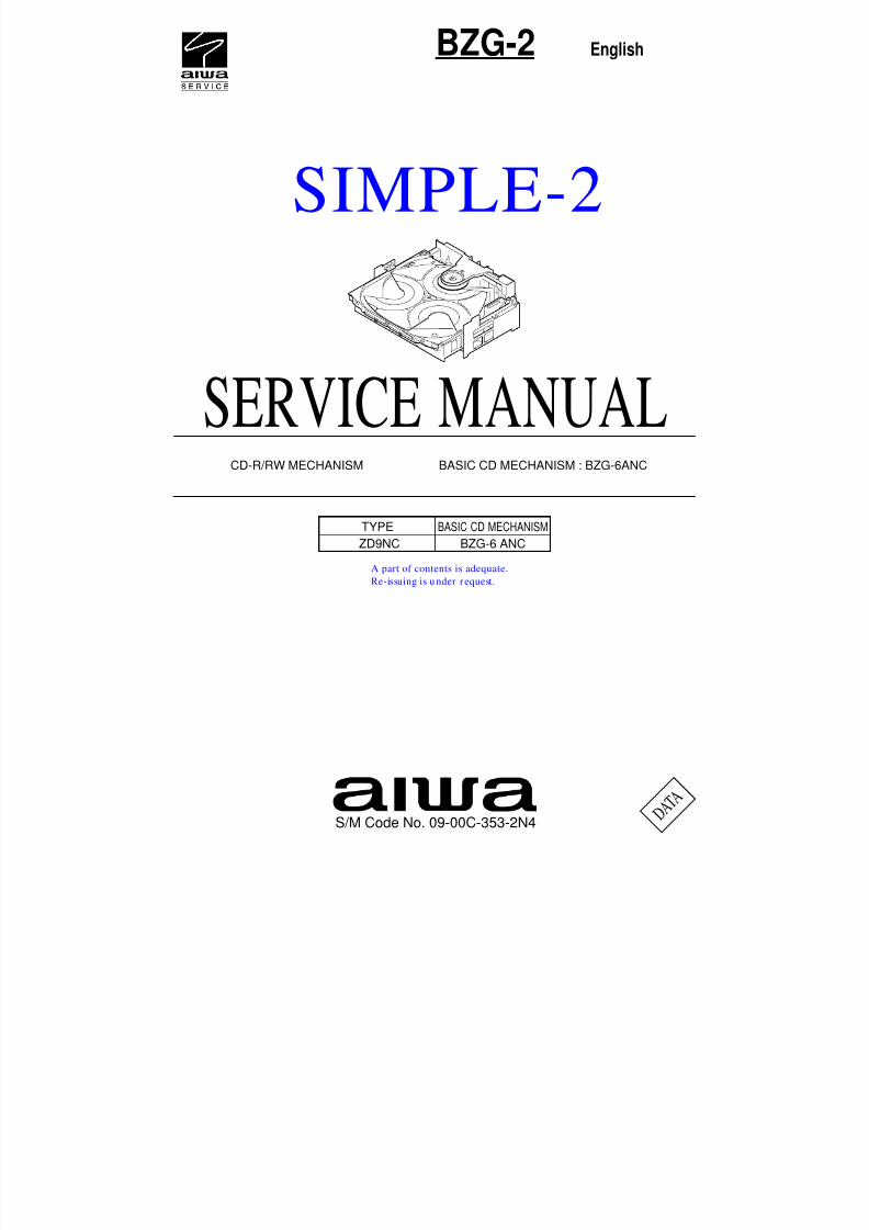
BZG-2
S/M Code No. 09-00C-353-2N4
English
SERVICE MANUALBASIC CD MECHANISM : BZG-6ANC
TYPE
ZD9NC
BASIC CD MECHANISM
BZG-6 ANC
D A T A
SIMPLE-2
A part of contents is adequate.
Re-issuing is u nder r equest.
8/9/2019 AIWA_BZG-2_SimpleSvcMnls-2
http://slidepdf.com/reader/full/aiwabzg-2simplesvcmnls-2 2/29
-2-
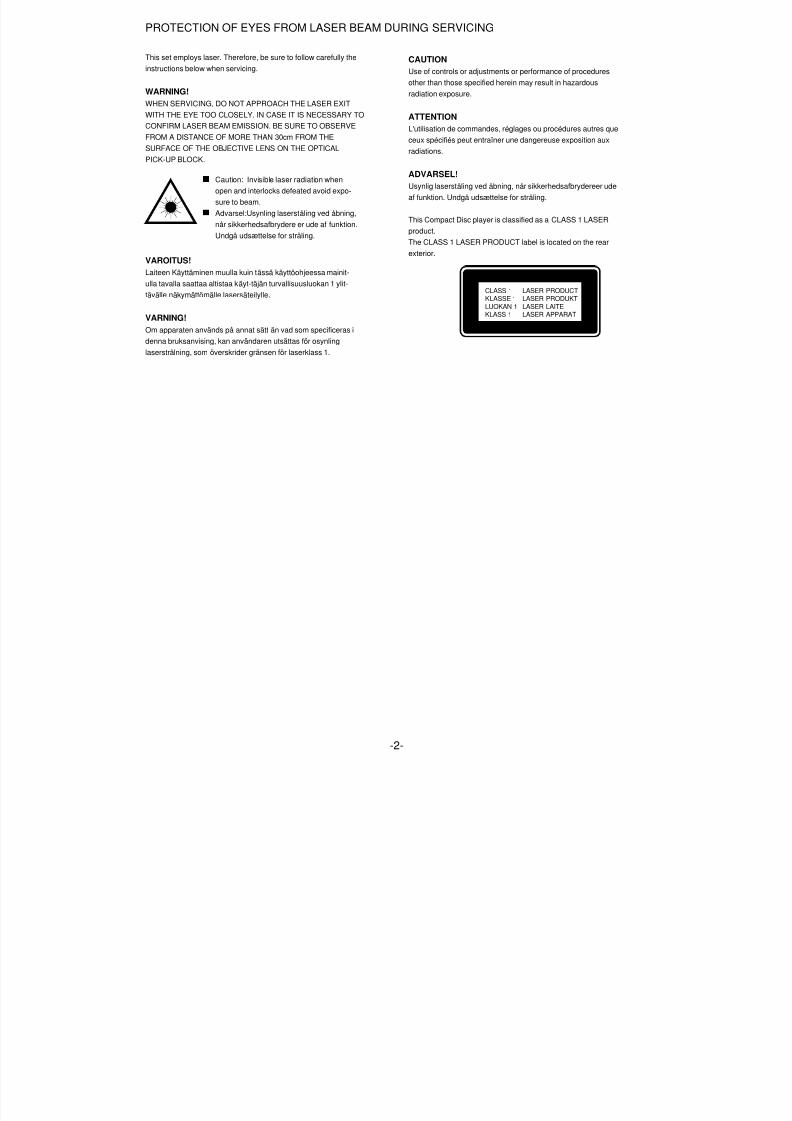
PROTECTION OF EYES FROM LASER BEAM DURING SERVICING
VAROITUS!
Laiteen Käyttäminen muulla kuin tässä käyttöohjeessa mainit-
ulla tavalla saattaa altistaa käyt-tä jän turvallisuusluokan 1 ylit-
tävälle näkymättömälle lasersäteilylle.
VARNING!
Om apparaten används på annat sätt än vad som specificeras i
denna bruksanvising, kan användaren utsättas för osynling
laserstrålning, som överskrider gränsen för laserklass 1.
Caution: Invisible laser radiation when
open and interlocks defeated avoid expo-
sure to beam.
Advarsel:Usynling laserståling ved åbning,
når sikkerhedsafbrydere er ude af funktion.
Undgå udsættelse for stråling.
CAUTION
Use of controls or adjustments or performance of procedures
other than those specified herein may result in hazardous
radiation exposure.
ATTENTION
L'utilisation de commandes, réglages ou procédures autres que
ceux spécifiés peut entra îner une dangereuse exposition aux
radiations.
ADVARSEL!
Usynlig laserståling ved åbning, når sikkerhedsafbrydereer ude
af funktion. Undgå udsættelse for stråling.
This Compact Disc player is classified as a CLASS 1 LASER
product.
The CLASS 1 LASER PRODUCT label is located on the rear
exterior.
This set employs laser. Therefore, be sure to follow carefully the
instructions below when servicing.
WARNING!
WHEN SERVICING, DO NOT APPROACH THE LASER EXIT
WITH THE EYE TOO CLOSELY. IN CASE IT IS NECESSARY TO
CONFIRM LASER BEAM EMISSION. BE SURE TO OBSERVE
FROM A DISTANCE OF MORE THAN 30cm FROM THESURFACE OF THE OBJECTIVE LENS ON THE OPTICAL
PICK-UP BLOCK.
CLASS 1KLASSE 1
LUOKAN 1KLASS 1
LASER PRODUCTLASER PRODUKT
LASER LAITELASER APPARAT
8/9/2019 AIWA_BZG-2_SimpleSvcMnls-2
http://slidepdf.com/reader/full/aiwabzg-2simplesvcmnls-2 3/29
-3-
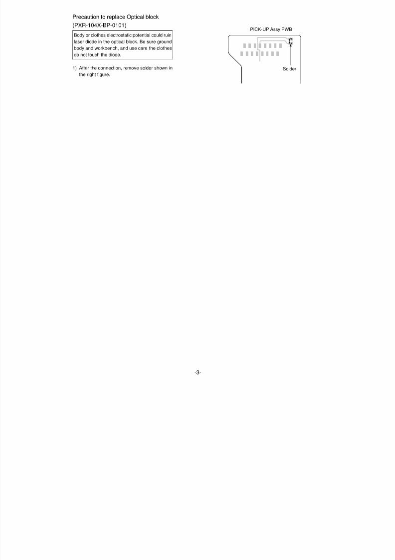
Precaution to replace Optical block
(PXR-104X-BP-0101)
1) After the connection, remove solder shown inthe right figure.
Body or clothes electrostatic potential could ruin
laser diode in the optical block. Be sure ground
body and workbench, and use care the clothes
do not touch the diode.
Solder
PICK-UP Assy PWB
8/9/2019 AIWA_BZG-2_SimpleSvcMnls-2
http://slidepdf.com/reader/full/aiwabzg-2simplesvcmnls-2 4/29
-4-
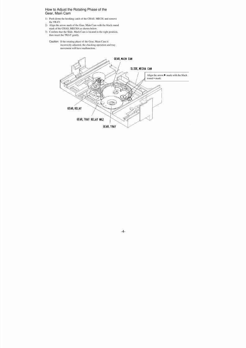
How to Adjust the Rotating Phase of theGear, Main Cam
1) Push down the hooking catch of the CHAS. MECH, and remove
the TRAY.
2) Align the arrow mark of the Gear, Main Cam with the black round
mark of the CHAS, MECHA as shown below.
3) Confirm that the Slide, Mech Cam is located in the right position,
then insert the TRAY gently.
Caution: If the rotating phase of the Gear, Main Cam is
incorrectly adjusted, the chucking operation and tray
movement will have malfunction.
Align the arrow 2 mark with the black
round • mark.
8/9/2019 AIWA_BZG-2_SimpleSvcMnls-2
http://slidepdf.com/reader/full/aiwabzg-2simplesvcmnls-2 5/29
8/9/2019 AIWA_BZG-2_SimpleSvcMnls-2
http://slidepdf.com/reader/full/aiwabzg-2simplesvcmnls-2 6/29

8/9/2019 AIWA_BZG-2_SimpleSvcMnls-2
http://slidepdf.com/reader/full/aiwabzg-2simplesvcmnls-2 7/29
8/9/2019 AIWA_BZG-2_SimpleSvcMnls-2
http://slidepdf.com/reader/full/aiwabzg-2simplesvcmnls-2 8/29

8/9/2019 AIWA_BZG-2_SimpleSvcMnls-2
http://slidepdf.com/reader/full/aiwabzg-2simplesvcmnls-2 9/29
-9
UNIT-NAME ! C REF-NO PARTS-NO PARTS-NAME SUFFIX&MODEL
! = ! SAFTY PARTSC = Components marked
All components used on this model at the production line are shown in this service manual.However, please note that not all components will be available as spare parts for after-sales service.Components marked S and O are designated as spare parts for service and will be stocked at the spare parts centers.Components marked X and R are not designated as spare parts for after sales service, and will not be stocked at the spare parts centers.
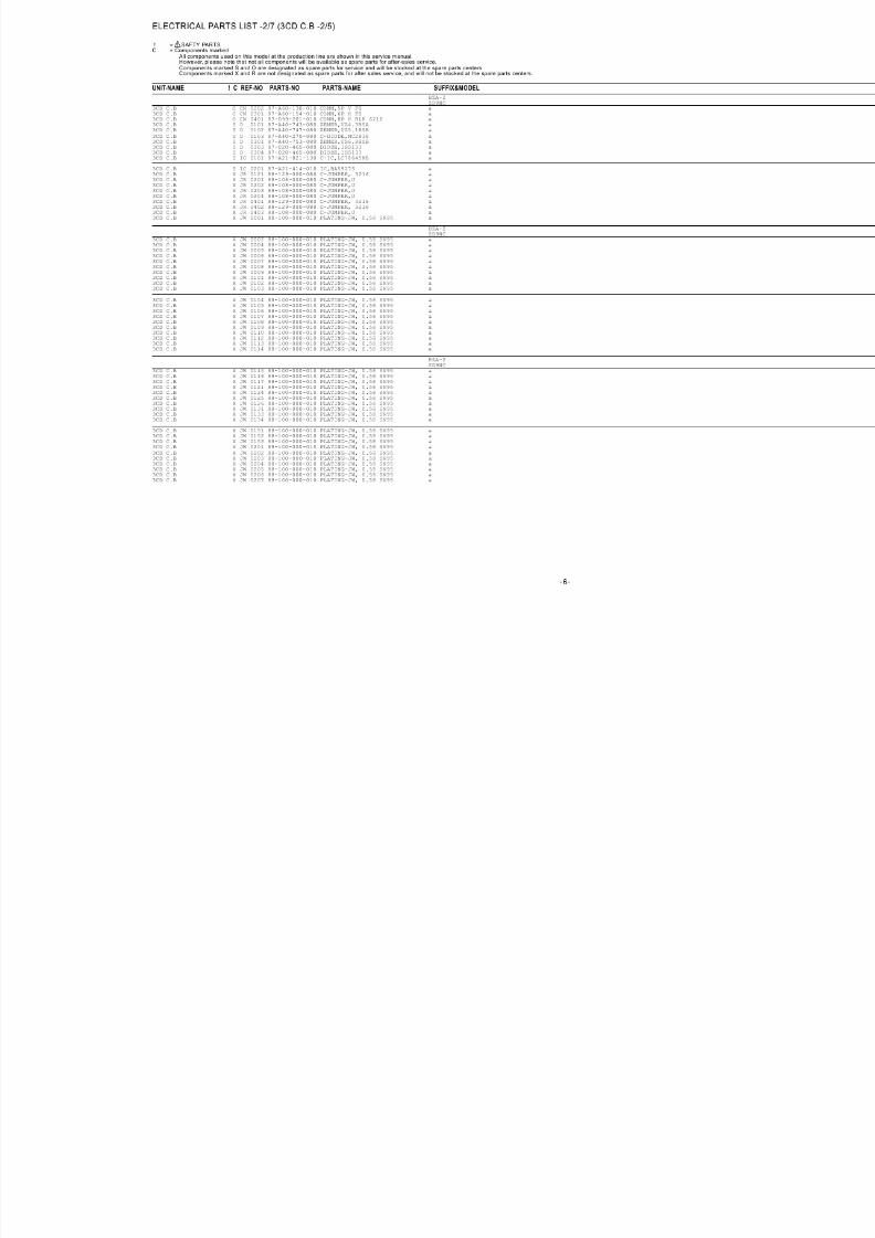
ELECTRICAL PARTS LIST -5/7 (3CD C.B -5/5)
BZA-2ZD9NC
3CD C.B X R 0312 88-128-109-080 C-RES, 1-1/8W J a3CD C.B X R 0313 88-128-109-080 C-RES, 1-1/8W J a3CD C.B X R 0314 88-128-109-080 C-RES, 1-1/8W J a3CD C.B X R 0401 88-108-101-080 C-RES,U 100-1/16W J a3CD C.B X R 0402 88-108-101-080 C-RES,U 100-1/16W J a3CD C.B X R 0403 88-108-101-080 C-RES,U 100-1/16W J a3CD C.B X R 0404 88-108-101-080 C-RES,U 100-1/16W J a3CD C.B X R 0405 88-108-101-080 C-RES,U 100-1/16W J a
3CD C.B X R 0406 88-108-101-080 C-RES,U 100-1/16W J a3CD C.B X R 0407 88-108-101-080 C-RES,U 100-1/16W J a
3CD C.B X R 0408 88-108-101-080 C-RES,U 100-1/16W J a3CD C.B X R 0415 88-108-182-080 C-RES,U 1.8K-1/16W J a3CD C.B X R 0416 88-121-122-080 RES,1.2K-1/8W J a3CD C.B X R 0417 88-108-562-080 C-RES,U 5.6K-1/16W J a3CD C.B O S 0401 87-036-109-010 SW,MICRO SPPB61 a3CD C.B O S 0402 87-036-109-010 SW,MICRO SPPB61 a3CD C.B O X 0101 87-A70-318-010 VIB,XTAL 33.8688MHZ CSA-309 a
8/9/2019 AIWA_BZG-2_SimpleSvcMnls-2
http://slidepdf.com/reader/full/aiwabzg-2simplesvcmnls-2 10/29
-1
UNIT-NAME ! C REF-NO PARTS-NO PARTS-NAME SUFFIX&MODEL
! = ! SAFTY PARTSC = Components marked
All components used on this model at the production line are shown in this service manual.However, please note that not all components will be available as spare parts for after-sales service.Components marked S and O are designated as spare parts for service and will be stocked at the spare parts centers.Components marked X and R are not designated as spare parts for after sales service, and will not be stocked at the spare parts centers.
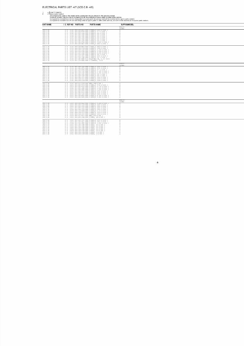
ELECTRICAL PARTS LIST -6/7 (T-T C.B/MOTOR C.B -1/1)
BZG-2ZD9NC
MOTOR C.B O CN 0001 87-A60-086-010 CONN,06P H 6216 aMOTOR C.B O M 0001 87-045-358-010 MOT,RF-310TA 43 aMOTOR C.B O M 0002 87-045-363-010 MOT,MDN4RA3ETA1 aMOTOR C.B O SW 0001 87-A90-042-010 SW,LEAF MSW-17310MVP0 aT-T C.B O C 0401 87-A11-148-080 CAP,TC U 0.1-50 Z F aT-T C.B O CN 0401 86-NFZ-675-010 CONN,5P H 6216-11H aT-T C.B O PS 0401 87-A90-156-010 SNSR,SG-240 aT-T C.B X R 0408 88-121-561-080 RES,560-1/8W J a
T-T C.B X R 0409 88-121-273-080 RES,27K-1/8W J a
8/9/2019 AIWA_BZG-2_SimpleSvcMnls-2
http://slidepdf.com/reader/full/aiwabzg-2simplesvcmnls-2 11/29
-11-
8 8
A
Resistor Code
Chip Resistor Part Coding
Figure
Value of resistor
Chip resistor
Wattage Type Tolerance
1/16W1/10W
1/8W
16082125
3216
5%5%
5%
CJCJ
CJ
Form L W t
1.6 0.8 0.45
2 1.25 0.45
3.2 1.6
108
118
128
: A: A
CHIP RESISTOR PART CODE
0.55
Resistor CodeDimensions (mm)
Symbol
1/16W 1005 5% CJ 1.0 0.5 0.35 104
L
t
W
• Regarding connectors, they are not stocked as they are not the initial order items.
The connectors are available after they are supplied from connector manufacturers upon the order is received.
ELECTRICAL PARTS LIST-7/7
8/9/2019 AIWA_BZG-2_SimpleSvcMnls-2
http://slidepdf.com/reader/full/aiwabzg-2simplesvcmnls-2 12/29
-12-
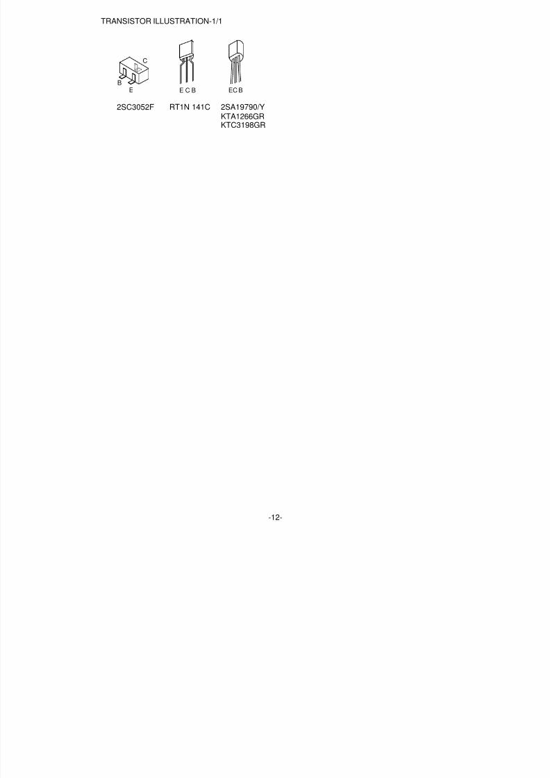
TRANSISTOR ILLUSTRATION-1/1
EC BE C BEB
C
2SC3052F 2SA19790/Y
KTA1266GR
RT1N 141C
KTC3198GR
8/9/2019 AIWA_BZG-2_SimpleSvcMnls-2
http://slidepdf.com/reader/full/aiwabzg-2simplesvcmnls-2 13/29
-13-
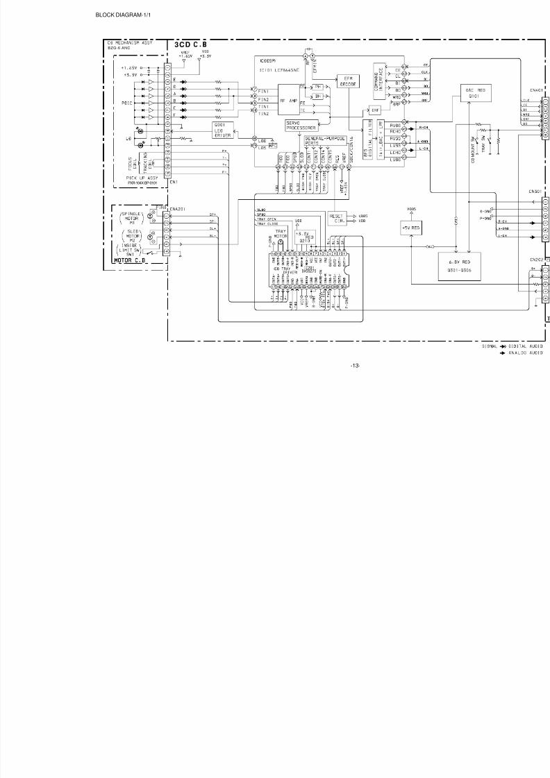
BLOCK DIAGRAM-1/1
BZG-6 ANC
PXR-104X-BP-0101
3CD
8/9/2019 AIWA_BZG-2_SimpleSvcMnls-2
http://slidepdf.com/reader/full/aiwabzg-2simplesvcmnls-2 14/29
-14-
1011121314151617181920212223242526272829303132
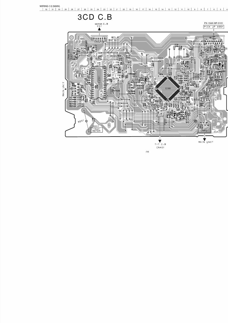
WIRING-1/2 (MAIN)
MOTOR
( T R A Y S W ) ( C
D M O U N T
S W )
3CD C.B
8/9/2019 AIWA_BZG-2_SimpleSvcMnls-2
http://slidepdf.com/reader/full/aiwabzg-2simplesvcmnls-2 15/29
-15-
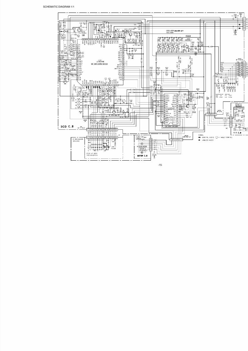
SCHEMATIC DIAGRAM-1/1
3CD
BZG-6 ANC
PXR-104X-BP-0101
8/9/2019 AIWA_BZG-2_SimpleSvcMnls-2
http://slidepdf.com/reader/full/aiwabzg-2simplesvcmnls-2 16/29
-16-
123456789101112131415
A
B
C
D
E
F
G
H
I
J
K
L
M
N
O
P
Q
R
S
T
U
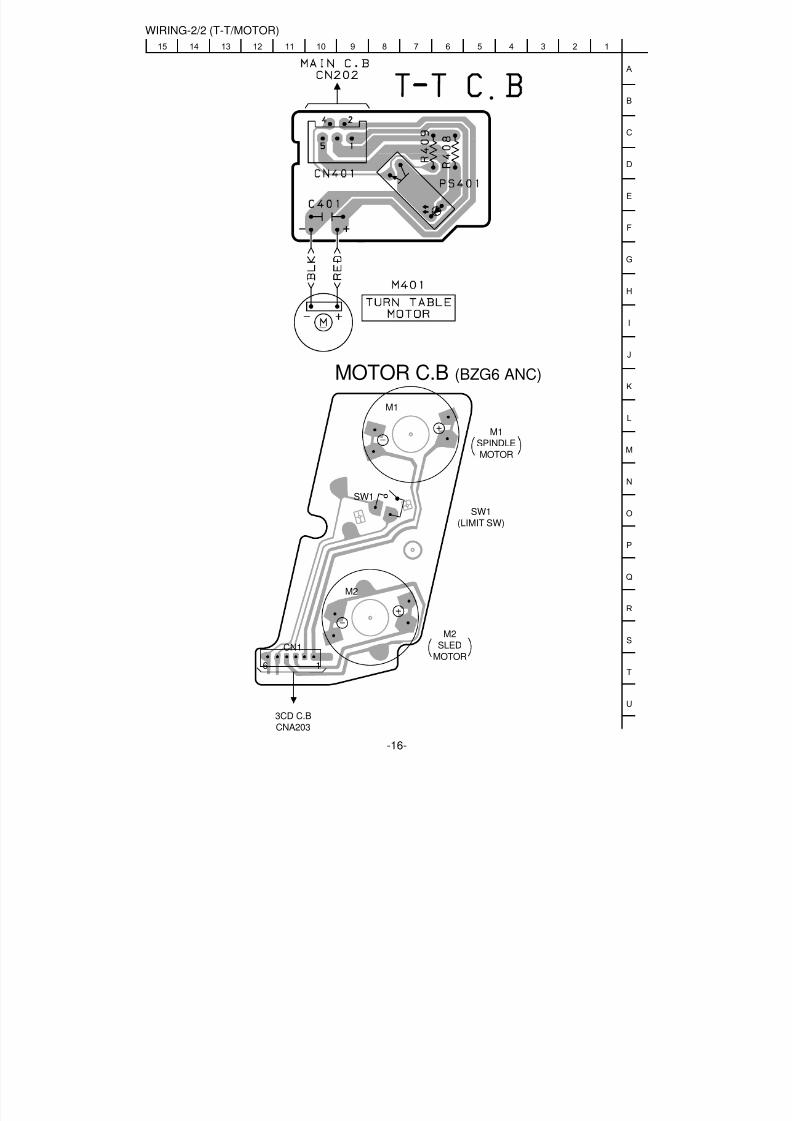
WIRING-2/2 (T-T/MOTOR)
MOTOR C.B (BZG6 ANC)
M1
SW1
M1
SPINDLE
MOTOR
M2
SLED
MOTOR
M2
SW1
(LIMIT SW)
CN1
16
3CD C.B
CNA203
8/9/2019 AIWA_BZG-2_SimpleSvcMnls-2
http://slidepdf.com/reader/full/aiwabzg-2simplesvcmnls-2 17/29
-17-
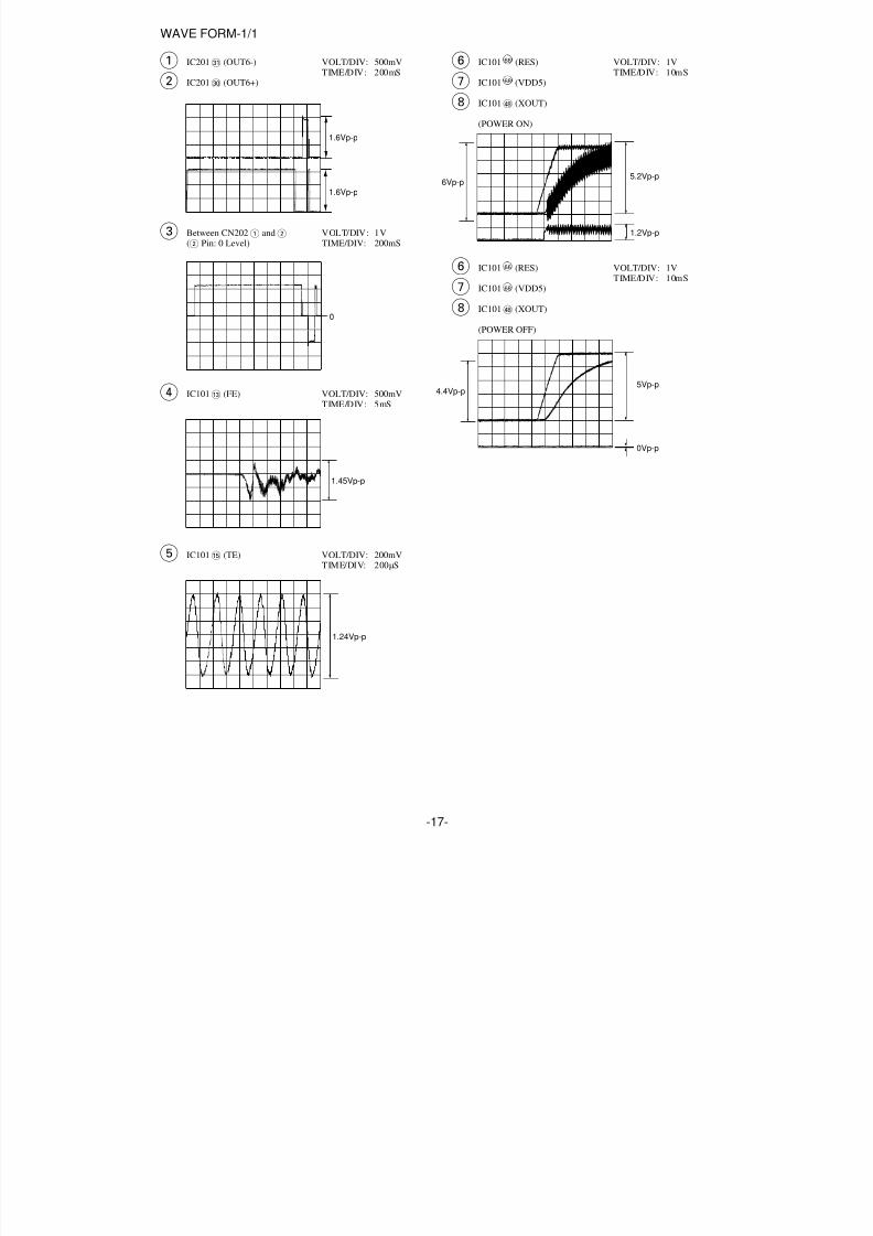
WAVE FORM-1/1
1 IC201⁄ (OUT6-) VOLT/DIV: 500mVTIME/DIV: 200mS
2 IC201º (OUT6+)
1.6Vp-p
1.6Vp-p
3 Between CN2021 and2 VOLT/DIV: 1V(2 Pin: 0 Level) TIME/DIV: 200mS
0
4 IC101# (FE) VOLT/DIV: 500mVTIME/DIV: 5mS
5 IC101% (TE) VOLT/DIV: 200mVTIME/DIV: 200µS
1.45Vp-p
1.24Vp-p
6 IC101 (RES) VOLT/DIV: 1VTIME/DIV: 10mS
7 IC101 (VDD5)
8 IC101? (XOUT)
(POWER ON)
6 IC101 (RES) VOLT/DIV: 1VTIME/DIV: 10mS
7 IC101 (VDD5)
8 IC101? (XOUT)
(POWER OFF)
6Vp-p5.2Vp-p
1.2Vp-p
4.4Vp-p5Vp-p
0Vp-p
66
68
66
68
8/9/2019 AIWA_BZG-2_SimpleSvcMnls-2
http://slidepdf.com/reader/full/aiwabzg-2simplesvcmnls-2 18/29
-18-
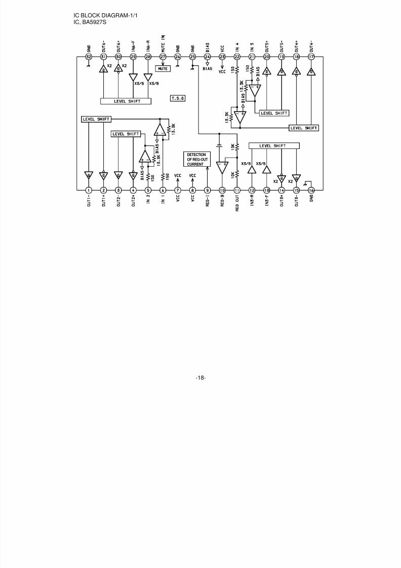
IC BLOCK DIAGRAM-1/1IC, BA5927S
DETECTION
OF REG-OUT
CURRENT

8/9/2019 AIWA_BZG-2_SimpleSvcMnls-2
http://slidepdf.com/reader/full/aiwabzg-2simplesvcmnls-2 19/29
-19-
1
2
3
4
5
6
7
8
9
10
11
12
13
14
15
16
17
18
19
20
21
22
23
24
25, 26
27
28
29
30
31
32-36
37
38
39
40
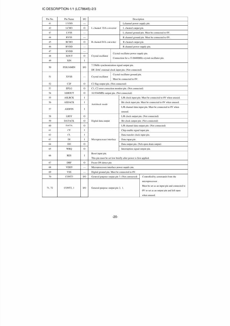
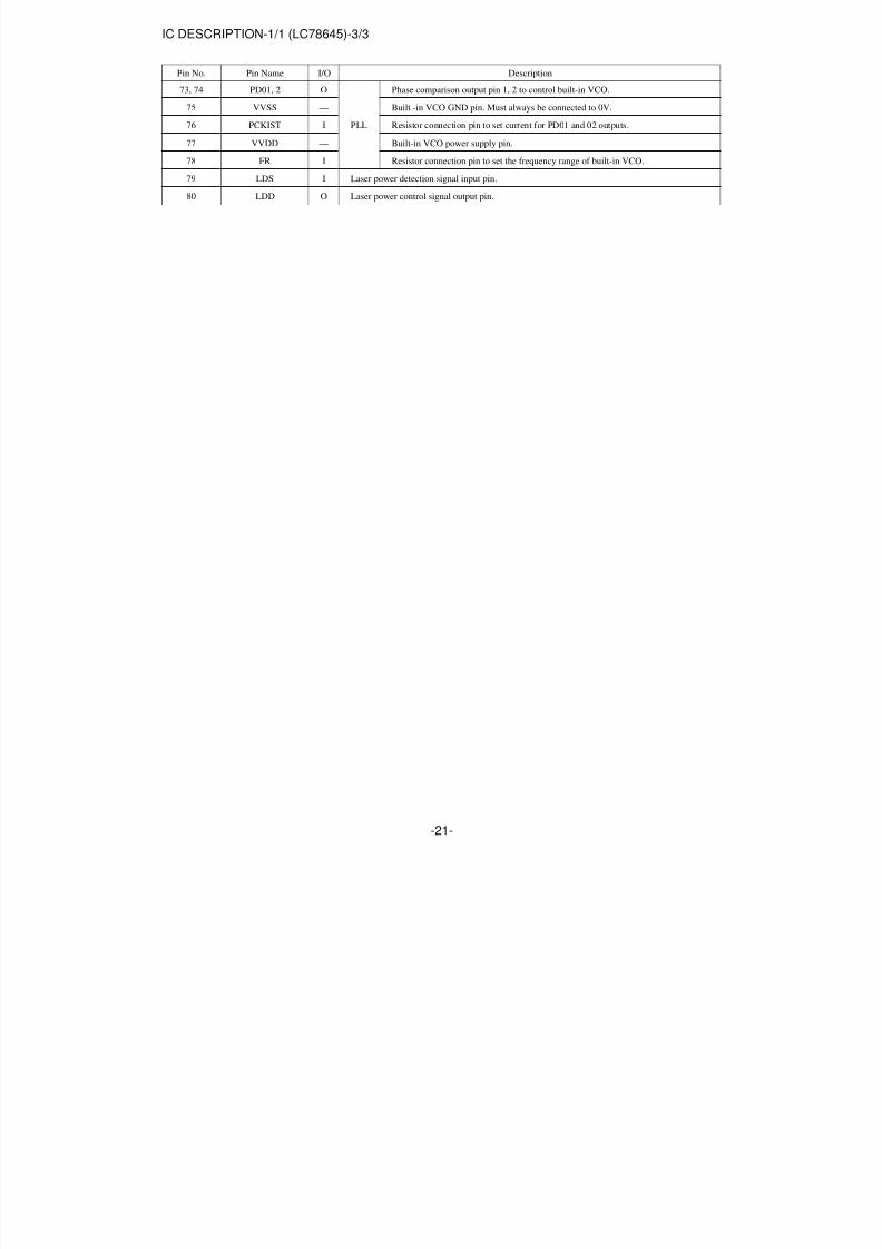
Pin No. Pin Name I/O Description
IC DESCRIPTION-1/1 (LC78645)-1/3
SLCO
SLCIST
EFMIN
RF
RFVDD
RFVSS
FIN1
FIN2
TIN1
TIN2
VREF
REFI
EF
TEC
TE
RFMON
JITTC
ADAVDD
ADAVSS
TDO
FDO
SPDO
SLDO
GPDAC
CONT4, 5
SBCK/CONT6
SBCK/FG
DEFECT
V/P
FSEQ
MONI1, 5
VSS
VDD
DOUT
TEST
O
I
I
O
—
—
I
I
I
I
O
I
O
O
O
O
O
—
—
O
O
O
O
O
I/O
I/O
I
O
O
O
O
—
—
O
I
Control output.
Slice level control SLCO output current adjustment resistor connection pin.
RF signal input pin.
RF monitor pin.
RF power supply pin.
RF ground pin. Must be connected to 0V.
A+C signal input pin.
B+D signal input pin.
E signal input pin.
F signal input pin.
VREF voltage output pin.
Reference voltage output setting pin.
FE signal monitor pin.
TE signal LPF capacitor connection pin.
TE signal monitor pin.
RF internal signal monitor pin.
Jitter detection capacitor connection pin.
Servo A/D, D/A supply pin.
Servo A/D, D/A ground pin. Must be connected to 0V.
Tracking control output pin. D/A output.
Focus control output pin. D/A output.
Spindle control output pin. D/A output.
Thread control output pin. D/A output.
Servo D/A general-purpose output pin. (Not connected)
General-purpose input/output pin 4, 5. Controlled by commands from the microprocessor.
General-purpose input/output pin 6,Any of these that are unused must be either set up as
or subcode read clock input pin.input pin ports and connected to 0V, or set up as
output pin ports and left open.
Subcode read clock input pin/FG signal input pin/external emphasis setting pin.
Set to command -pin function. Must be connected to 0V.
Defect pin. (Not connected)
Rouge servo/phase control automatic switching monitor output pin.
“H” for rough servo and “L” for phase servo. (Not connected)
Synchronization signal detection output pin.
Outputs a high level when the synchronization signal detected from the EFM signal and the
internally generated synchronization signal agree. (Not connected)
Internal signal monitor pin 1, 5. (Not connected)
Digital ground pin. Must be connected to 0V.
Digital power supply pin.
Digital OUT output pin. (Not connected)
Test input pin. Must be connected to 0V.
8/9/2019 AIWA_BZG-2_SimpleSvcMnls-2
http://slidepdf.com/reader/full/aiwabzg-2simplesvcmnls-2 20/29
-20-
Pin No. Pin Name I/O Description
41
42
43
44
45
46
47
48
49
50
51
52
53
54
55
56
57
58
59
60
61
62
63
64
65
66
67
68
69
70
71, 72
IC DESCRIPTION-1/1 (LC78645)-2/3
LVDD
LCHO
LVSS
RVSS
RCHO
RVDD
XVDD
XOUT
XIN
FSX/16MIN
XVSS
C2F
EFLG
16MOUT
ASLRCK
ASDACK
ASDFIN
LRSY
DATACK
DATA
CE
CL
DI
DO
WRQ
RES
DRF
VDD5
VSS
CONT3
CONT2, 1
—
O
—
—
O
—
—
O
I
I/O
—
O
O
O
I
I
I
O
O
O
I
I
I
O
O
I
O
—
—
I/O
I/O
Lchannel power supply pin.
L channel D/A converter L channel output pin.
L channel ground pin. Must be connected to 0V.
R channel ground pin. Must be connected to 0V.
R channel D/A converter R channel output pin.
R channel power supply pin.
Crystal oscillator power supply pin.Crystal oscillator
Connection for a 33.8688MHz crystal oscillator pin.
7.35kHz synchronization signal output pin.
DF, DAC external clock input pin. (Not connected)
Crystal oscillatorCrystal oscillator ground pin.
Must be connected to 0V.
C2 flag output pin. (Not connected)
C1, C2 error correction monitor pin. (Not connected)
16.9344MHz output pin. (Not connected)
L/R clock input pin. Must be connected to 0V when unused.
Antishock modeBit clock input pin. Must be connected to 0V when unused.
L/R channel data input pin. Must be connected to 0V when
unused.
L/R clock output pin. (Not connected)
Digital data output Bit clock output pin. (Not connected)
L/R channel data output pin. (Not connected)
Chip enable signal input pin.
Data transfer clock input pin.
Microprocessor interface Data input pin.
Data output pin. (Nch open drain output)
Interruption signal output pin.
Reset input pin.
This pin must be set low briefly after power is first applied.
Focus ON detect pin.
Microprocessor interface power supply pin.
Digital ground pin. Must be connected to 0V.
General-purpose output pin 3. (Not connected) Controlled by commands from the
microprocessor .
General-purpose output pin 2, 1.Must be set as an input pin and connected to
0V or set as an output pin and left open
when unused.
8/9/2019 AIWA_BZG-2_SimpleSvcMnls-2
http://slidepdf.com/reader/full/aiwabzg-2simplesvcmnls-2 21/29
-21-
Pin No. Pin Name I/O Description
IC DESCRIPTION-1/1 (LC78645)-3/3
73, 74
75
76
77
78
79
80
PD01, 2
VVSS
PCKIST
VVDD
FR
LDS
LDD
O
—
I
—
I
I
O
Phase comparison output pin 1, 2 to control built-in VCO.
Built -in VCO GND pin. Must always be connected to 0V.
PLL Resistor connection pin to set current for PD01 and 02 outputs.
Built-in VCO power supply pin.
Resistor connection pin to set the frequency range of built-in VCO.
Laser power detection signal input pin.
Laser power control signal output pin.
8/9/2019 AIWA_BZG-2_SimpleSvcMnls-2
http://slidepdf.com/reader/full/aiwabzg-2simplesvcmnls-2 22/29
-22-
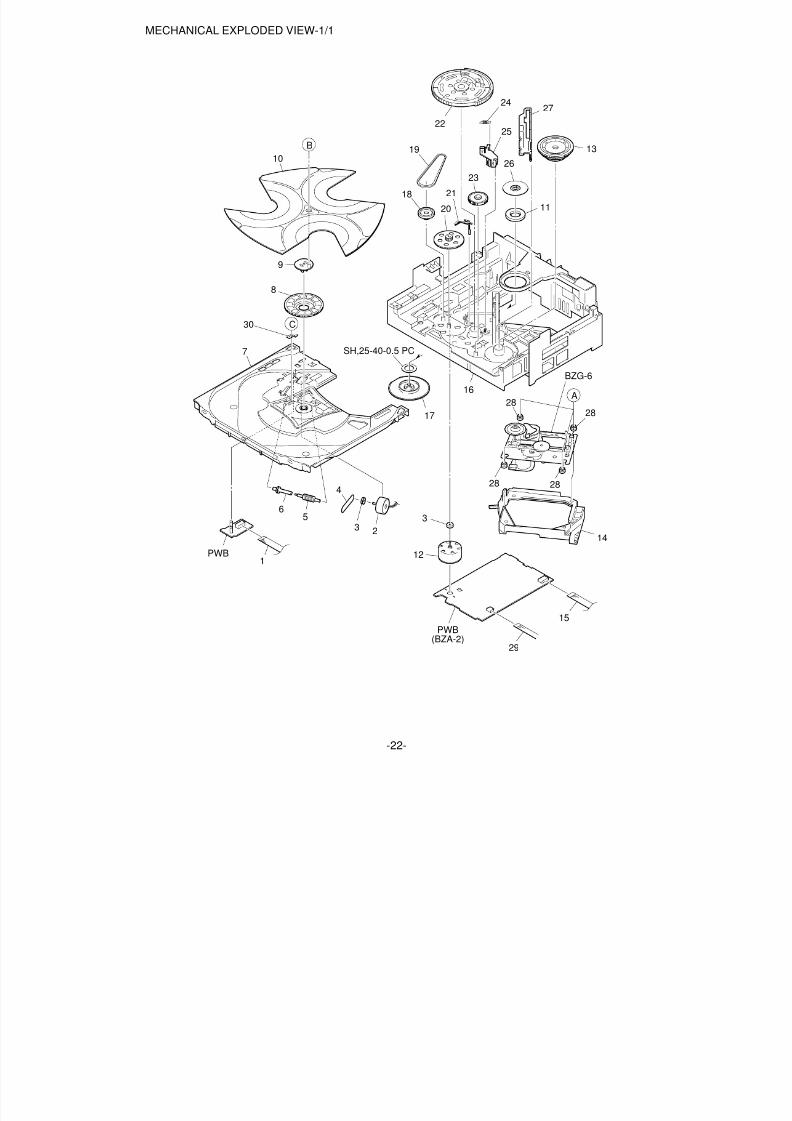
MECHANICAL EXPLODED VIEW-1/1
1PWB
PWB(BZA-2)
23
4
56
7
30
8
9
10
15
12
3
14
A16
17
18
19
20
21
22
23
24
25
26
27
13
11
B
C
BZG-6
SH,25-40-0.5 PC
28 28
28
28
29
8/9/2019 AIWA_BZG-2_SimpleSvcMnls-2
http://slidepdf.com/reader/full/aiwabzg-2simplesvcmnls-2 23/29
8/9/2019 AIWA_BZG-2_SimpleSvcMnls-2
http://slidepdf.com/reader/full/aiwabzg-2simplesvcmnls-2 24/29
-24-
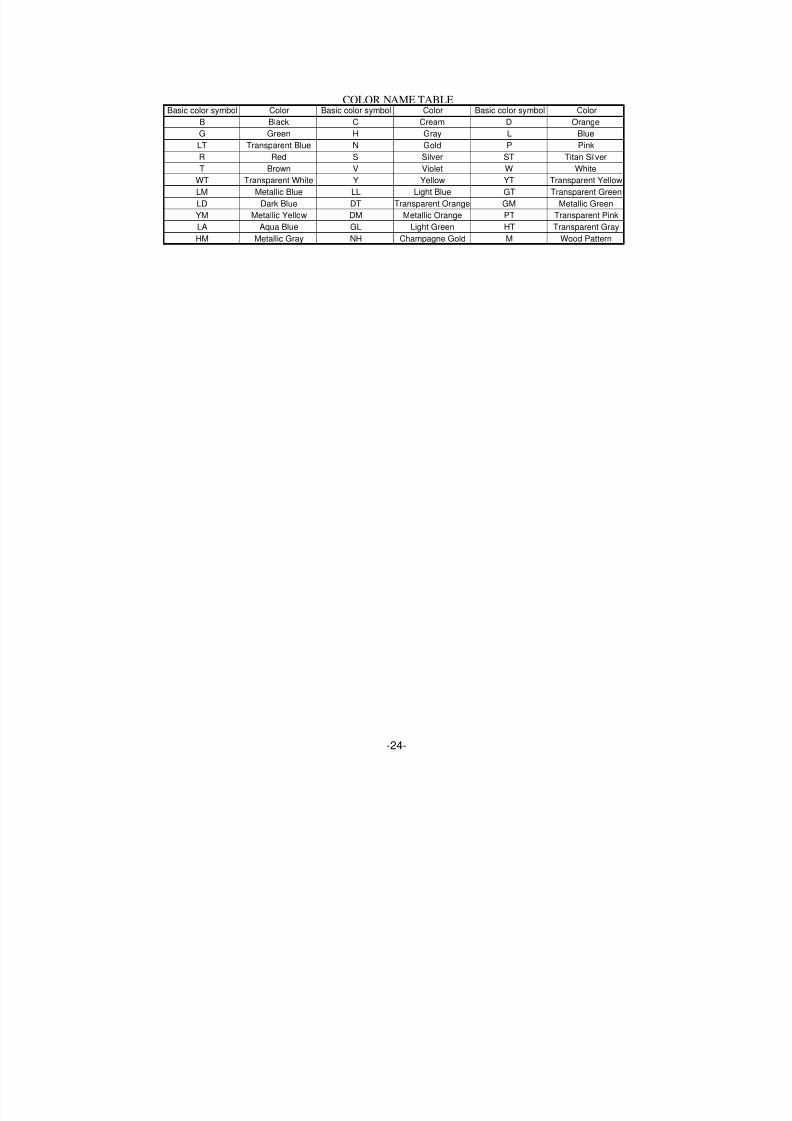
COLOR NAME TABLEBasic color symbol Color Basic color symbol Color Basic color symbol Color
B Black C Cream D Orange
G Green H Gray L Blue
LT Transparent Blue N Gold P Pink
R Red S Silver ST Titan Silver
T Brown V Violet W White
WT Transparent White Y Yellow YT Transparent Yellow
LM Metallic Blue LL Light Blue GT Transparent Green
LD Dark Blue DT Transparent Orange GM Metallic Green
YM Metallic Yellow DM Metallic Orange PT Transparent Pink
LA Aqua Blue GL Light Green HT Transparent Gray
HM Metallic Gray NH Champagne Gold M Wood Pattern
8/9/2019 AIWA_BZG-2_SimpleSvcMnls-2
http://slidepdf.com/reader/full/aiwabzg-2simplesvcmnls-2 25/29
-25-
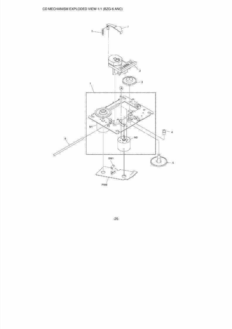
CD MECHANISM EXPLODED VIEW-1/1 (BZG-6 ANC)
A
3
6
2
5
1
PWB
M2
SW1
4
7
8
M1
8/9/2019 AIWA_BZG-2_SimpleSvcMnls-2
http://slidepdf.com/reader/full/aiwabzg-2simplesvcmnls-2 26/29
-26-
REF. NO PART NO. KANRI DESCRIPTION
NO.
CD MECHANISM PARTS LIST-1/1 (BZG-6 ANC)
1 83-ZG2-243-310 CHAS ASSY,SHT2 87-A92-037-010 PICKUP,PXR-104X-BP-0101
3 83-ZG2-235-010 GEAR,A34 83-ZG2-236-010 GEAR,MOTOR 3
5 83-ZG2-205-210 GEAR,B
6 83-ZG2-253-110 SHAFT,SLIDE 5
7 83-ZG2-245-510 LEVER,SHUTTER(*)8 83-ZG2-250-210 SPR-E,SHT 2
A 87-261-032-210 V+2-3

8/9/2019 AIWA_BZG-2_SimpleSvcMnls-2
http://slidepdf.com/reader/full/aiwabzg-2simplesvcmnls-2 27/29
-2
UNIT-NAME ! C REF-NO PARTS-NO PARTS-NAME SUFFIX&MODEL
! = ! SAFTY PARTSC = Components marked
All components used on this model at the production line are shown in this service manual.However, please note that not all components will be available as spare parts for after-sales service.Components marked S and O are designated as spare parts for service and will be stocked at the spare parts centers.Components marked X and R are not designated as spare parts for after sales service, and will not be stocked at the spare parts centers.
OTHER PARTS LIST -1/2 (BZG-2)-1/1
BZG-2ZD9NC
ASSY CODE X M8-BZG-296-170 BZG-2 ZD9NC aCD MECHANISM X M8-BZG-691-070 BZG-6 ANC aCD TRANSPORT X 8A-ZG1-214-010 SH, 25-40-0.5 PC aCD TRANSPORT X 8B-ZG2-255-010 SH, 7-5.5-0.5 W/ADH aELECTRICAL X A8-BZA-293-070 BZA-2 ZD9NC aPWB X 8B-ZG2-605-010 PWB,COMB T-T 28M aPWB X 8B-ZG2-606-010 PWB,T-T a
8/9/2019 AIWA_BZG-2_SimpleSvcMnls-2
http://slidepdf.com/reader/full/aiwabzg-2simplesvcmnls-2 28/29
-2
UNIT-NAME ! C REF-NO PARTS-NO PARTS-NAME SUFFIX&MODEL
! = ! SAFTY PARTSC = Components marked
All components used on this model at the production line are shown in this service manual.However, please note that not all components will be available as spare parts for after-sales service.Components marked S and O are designated as spare parts for service and will be stocked at the spare parts centers.Components marked X and R are not designated as spare parts for after sales service, and will not be stocked at the spare parts centers.
OTHER PARTS LIST -2/2 (BZA-2)-1/1
BZA-2ZD9NC
ASSY CODE X A8-BZA-293-070 BZA-2 ZD9NC aPWB X 8B-ZA2-605-210 PWB,COMB BZA2C 2M aPWB X 8B-ZA2-606-210 PWB,MAIN BZA2C a
8/9/2019 AIWA_BZG-2_SimpleSvcMnls-2
http://slidepdf.com/reader/full/aiwabzg-2simplesvcmnls-2 29/29


![[XLS] · Web view3 3 3 3 3 3 3 3 3 3 2 4 4 4 4 4 2 2 2 3 3 3 3 3 3 3 3 3 2 2 2 2 2 2 2 2 2 2 2 2 2 2 2 2 2 2 2 2 3 3 3 3 3 3 3 3 3 3 3 2 2 2 2 4 4 4 4 4 4 4 4 4 4 2 2 2 2 2 2 2 2](https://img.pdfslide.tips/doc/110x75/5b1aa0e07f8b9a3c258de1b1/xls-web-view3-3-3-3-3-3-3-3-3-3-2-4-4-4-4-4-2-2-2-3-3-3-3-3-3-3-3-3-2-2-2.jpg)