Embed Size (px)
Citation preview
ProgramKey
Program Key 1
Conference Topics AA ALD Applications AF ALD Fundamentals ALE Atomic Layer Etching AM ALD for Manufacturing AS Area Selective ALD EM Emerging Materials NS Nanostructure Synthesis and Fabrication PS Plenary Session
ProgramOverview
Program Overview 2
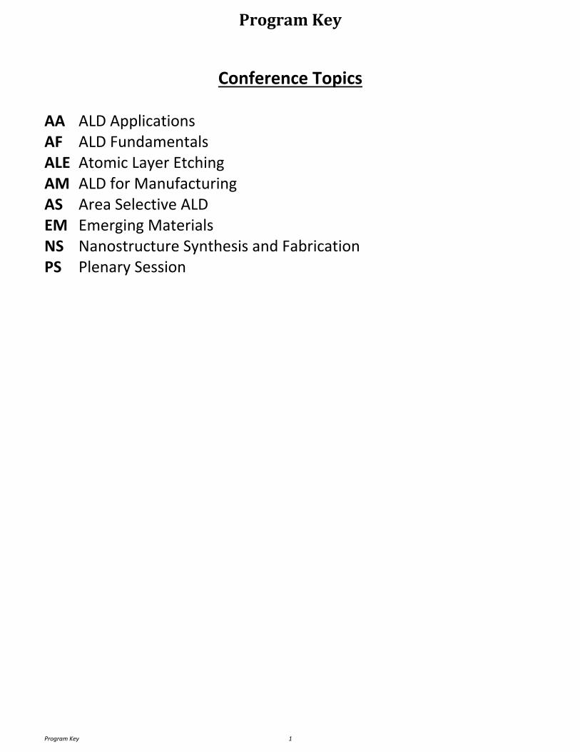
Room /Time
Plaza ABC Plaza D Plaza E Plaza Exhibit Plaza F
SaP
Poster Sessions
SuM PS1‐SuM: Sunday Plenary Session I
PS2‐SuM: Sunday Plenary Session II
SuA NS+EM‐SuA: 2D Materials
(1:30‐3:30 pm)/ Laminate,
Multicomponent, and Emerging Materials
(4:00‐5:30 pm)
ALE‐SuA: Atomic Layer Etching Session I (1:30‐3:30 pm) and II (4:00‐5:30 pm)
AF‐SuA: ALD Fundamentals: Precursors and
Mechanisms (1:30‐3:30 pm)/High Aspect Ratios & High Surface Areas
(4:00‐5:30 pm)
AS‐SuA: Area Selective Deposition I:
Deactivation (1:30‐3:30 pm)/Inherent Selectivity, Activation, Deactivation
(4:00‐5:30 pm)
SuP
Poster Sessions
MoM AA‐MoM:
Solar Materials I (8:00‐10:00 am)/Solar
Materials II (10:45 am‐12:00 pm)
ALE‐MoM:
Atomic Layer Etching Session III (8:00‐10:00 am) and Session IV (10:45 am‐12:00 pm)
AA+NS‐MoM: Energy: Catalysis and Fuel Cells I (8:00‐10:00 am)/Nanoparticles and Nanostructures (10:45
am‐12:00 pm)
AF+AA‐MoM: ALD Fundamentals:
Plasma ALD (8:00‐10:00 am)/Emerging
Applications (10:45 am‐12:00 pm)
MoA AA‐MoA:
Memory and MIM I (1:30‐3:30 pm)/
Memory and MIM II (4:00‐5:30 pm)
ALE+AF‐MoA: Atomic Layer Etching Session V (1:30‐3:30
pm)/ ALD Fundamentals: Process Development
(4:00‐5:45 pm)
EM+AA‐MoA: Organic‐Inorganic Hybrid Materials & MLD (1:30‐
3:30 pm)/ Catalysis and Fuel Cells II
(4:00‐5:30 pm)
AF‐MoA: ALD Fundamentals:
Characterization (1:30‐3:30 pm)/Mechanisms and Surface Science
(4:00‐5:00 pm)
MoP
Poster Sessions
TuM AA‐TuM:
Batteries I (8:00‐10:00 am)/Emerging Apps II (10:45 am‐12:00 pm)
AF2‐TuM: ALD Fundamentals: Theory & Mechanism
(8:00‐10: am)/Emerging Materials and Devices (10:45 am‐12:00 pm)
AF1‐TuM: ALD Fundamentals:
Precursors and Process Development (8:00‐10:00 am)/Precursors
and Mechanism (10:45am‐12:00 pm)
AA+AF‐TuM: Displays and Flexible
Applications (8:00‐10:00 am)/ALD Fundamentals: In‐Situ Monitoring and
Analysis (10:45 am‐12:00 pm)
TuA AA1‐TuA:
Batteries II (1:30‐3:30 pm)/Emerging Apps III
(4:00‐5:00 pm)
AA2‐TuA:
ULSI, High‐k and III‐V I (1:30‐3:30 pm)/
ULSI, High‐k and III‐V II (4:00‐5:00 pm)
AM+EM‐TuA:
ALD for Manufacturing (1:30‐3:30 pm)/MLD II
(4:00‐5:00 pm)
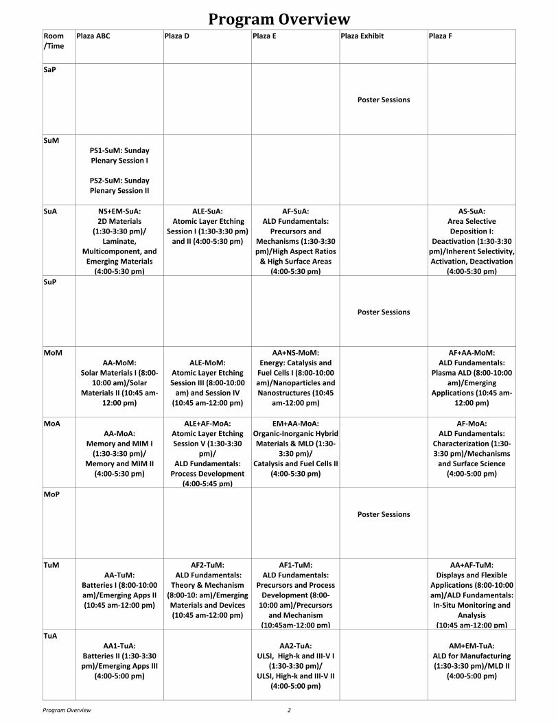
SaturdayEveningPosterSessions,July15,2017
Saturday Evening Poster Sessions, July 15, 2017 3 6:00 PM
Atomic Layer Etching Room Plaza Exhibit ‐ Session ALE‐SaP Atomic Layer Etching Poster Session 6:00pm
ALE‐SaP1 Quasi‐Atomic Layer Etching of Silicon Nitride with Tunable Directionality and Ultra‐high Selectivity, Sonam Sherpa, A. Ranjan, Tokyo Electron
ALE‐SaP2 Atomic Layer Etching with Gas Cluster Ion Beam Irradiation in Reactive Gas Vapor, Noriaki Toyoda, University of Hyogo, Japan; A. Ogawa, University of Hyogo; I. Yamada, Univeristy of Hyogo
ALE‐SaP3 Thermal Atomic Layer Etching of TiO2 using Sequential Exposures of WF6 and BCl3, P. Lemaire, Gregory N. Parsons, North Carolina State University
ALE‐SaP4 Etch Profile Control of ALD‐SiO2 Film Assisted by Alternating ALE Process of Fluorocarbon Deposition and O2 Plasma Etching, Masaru Zaitsu,
ASM, Japan; T. Tsutsumi, Nagoya University, Japan; A. Kobayashi, ASM; H. Kondo, M. Hori, Nagoya University, Japan; T. Nozawa, N. Kobayashi, ASM
ALE‐SaP5 In Situ Mass Spectrometer Studies of Volatile Etch Products During Thermal Al2O3 Atomic Layer Etching Using HF and Trimethylaluminum, Joel
Clancey, S.M. George, University of Colorado ‐ Boulder
ALE‐SaP6 Cyclic Plasma Cleaning Process of SiO2 Layers using Surface Fluorination, Kyongbeom Koh, H. Chae, Sungkyunkwan University (SKKU), Republic of
Korea
ALE‐SaP7 Low Damage Cyclical Etching of GaN and AlGaN, A. Goodyear, Oxford Instruments Plasma Technology, UK; P. Abrami, University of Bristol, UK; Mike Cooke, M. Loveday, Oxford Instruments Plasma Technology
ALE‐SaP8 Thermal Atomic Layer Etching of ZnO by “Conversion‐Etch” Using Hydrogen Fluoride and Trimethylaluminum, David Zywotko, S.M. George,
University of Colorado ‐ Boulder
ALE‐SaP9 Cryogenic Atomic Layer Etching of SiO2, N. Holtzer, Thomas Tillocher,
P. Lefaucheux, R. Dussart, GREMI Université d'Orléans/CNRS, France
ALE‐SaP10 SF4 as a New Fluorine Reagent for Thermal ALE: Application to Al2O3 and VO2 ALE, Jonas Gertsch, N. Johnson, V. Bright, S.M. George, University of
Colorado ‐ Boulder
ALE‐SaP11 Demonstrating Manufacturability of Atomic Level Etch (ALE) through Accelerated Neutral Atom Beam (ANAB) Processing, Daniel Steinke, B. Sapp, S. PapaRao, SUNY Polytechnic Institute; E. Barth, SEMATECH; V. Kaushik, M. Rodgers, C. Hobbs, SUNY Polytechnic Institute; M. Walsh, S. Kirkpatrick, R. Svrluga, Neutral Physics Corporation
ALE‐SaP12 Etching with Low Te Plasmas, Scott Walton, D. Boris, U.S. Naval
Research Laboratory; S. Hernández, U.S.Naval Research Laboratory; H. Miyazoe, A. Jagtiani, S. Engelmann, E. Joseph, IBM TJ Watson Research Center
ALE‐SaP13 Surface Cleaning of Gallium Antimonide Oxides: The Role of Hydrogen Atoms, Argon Ions, and Temperature, Thomas Larrabee, S. Prokes,
Naval Research Laboratory
ALE‐SaP14 Aluminum Native Oxide Surface Cleaning and Passivation in an Atmospheric Plasma System, John Mudrick, M. Pohl, K. Knisely, Sandia National
Laboratories
ALE‐SaP15 Atomic Layer Etching in Reactive Ion Etching System for Nanoscale Pattern Transfer, S. Khan, Dmitry Suyatin, M. Graczyk, A. Kvennefors,
Lund University, Sweden; E. Kauppinen, Aalto University, Finland; M. Huffman, I. Maximov, Lund University, Sweden; J. Sundqvist, Fraunhofer Institute for Ceramic Technologies and Systems IKTS, Germany
ALE‐SaP16 Selective Fluorocarbon‐based Atomic Layer Etching in a Conventional Parallel‐Plate, Capacitively Coupled Plasma, Stefano Dallorto, Ilmenau University of Technology; A. Goodyear, Oxford Instruments Plasma Technology, UK; M. Cooke, Oxford Instruments Plasma Technology; S. Dhuey, A. Schwartzberg, S. Sassolini, Lawrence Berkeley National Laboratory; C. Ward, Oxford Instruments; D. Olynick, Lawrence Berkeley National Laboratory; I. Rangelow, Ilmenau University of Technology; S. Cabrini, Lawrence Berkeley National Laboratory
ALE‐SaP17 RF Plasma Electrostatics: The Influence on Film Morphology and Carbon Incorporation, K. Scott Butcher, Meaglow Ltd, Canada; P. Terziyska, Institute
of Solid State Physics, Bulgarian Academy of Sciences, Bulgaria; V. Georgiev, Meaglow Ltd, Canada; D. Georgieva, Semiconductor Research Lab, Lakehead University, Canada; R,. Gergova, Central Laboratory of Solar Energy and New Energy Sources, Bulgarian Academy of Sciences, Bulgaria; P. Binsted, S. Skergetc, Semiconductor Research Lab, Lakehead University, Canada
ALE‐SaP18 Atomic Layer Etching of Amorphous Silicon with Selectivity Towards MoS2, Markus Heyne, KU Leuven, Belgium; A. Goodyear, Oxford
Instruments Plasma Technology, UK; J.‐F. de Marneffe, IMEC, Belgium; M. Cooke, Oxford Instruments Plasma Technology, UK; I. Radu, IMEC, Belgium; E. Neyts, University of Antwerp, Belgium; S. De Gendt, KU Leuven, Belgium
ALE‐SaP19 Simulation of New Material‐Systems for Directional Atomic Layer Etching, Ivan Berry, K.J. Kanarik, T. Lill, V. Vahedi, R. Gottscho, Lam Research Corp.
SundayMorning,July16,2017
Sunday Morning, July 16, 2017 4 8:00 AM
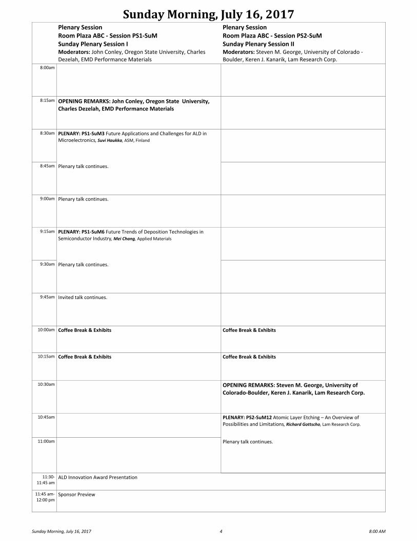
Plenary Session Room Plaza ABC ‐ Session PS1‐SuM Sunday Plenary Session I Moderators: John Conley, Oregon State University, Charles Dezelah, EMD Performance Materials
Plenary SessionRoom Plaza ABC ‐ Session PS2‐SuM Sunday Plenary Session II Moderators: Steven M. George, University of Colorado ‐ Boulder, Keren J. Kanarik, Lam Research Corp.
8:00am
8:15am OPENING REMARKS: John Conley, Oregon State University, Charles Dezelah, EMD Performance Materials
8:30am PLENARY: PS1‐SuM3 Future Applications and Challenges for ALD in Microelectronics, Suvi Haukka, ASM, Finland
8:45am Plenary talk continues.
9:00am Plenary talk continues.
9:15am PLENARY: PS1‐SuM6 Future Trends of Deposition Technologies in Semiconductor Industry, Mei Chang, Applied Materials
9:30am Plenary talk continues.
9:45am Invited talk continues.
10:00am Coffee Break & Exhibits Coffee Break & Exhibits
10:15am Coffee Break & Exhibits Coffee Break & Exhibits
10:30am OPENING REMARKS: Steven M. George, University of Colorado‐Boulder, Keren J. Kanarik, Lam Research Corp.
10:45am PLENARY: PS2‐SuM12 Atomic Layer Etching – An Overview of Possibilities and Limitations, Richard Gottscho, Lam Research Corp.
11:00am Plenary talk continues.
11:30‐11:45 am
ALD Innovation Award Presentation
11:45 am‐12:00 pm
Sponsor Preview
SundayAfternoon,July16,2017
Sunday Afternoon, July 16, 2017 5 1:30 PM
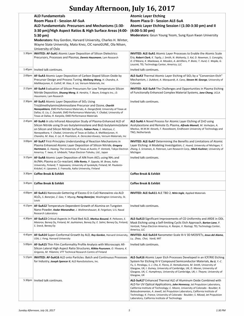
ALD Fundamentals Room Plaza E ‐ Session AF‐SuA ALD Fundamentals: Precursors and Mechanisms (1:30‐3:30 pm)/High Aspect Ratios & High Surface Areas (4:00‐5:30 pm) Moderators: Roy Gordon, Harvard University, Charles H. Winter, Wayne State University, Mato Knez, CIC nanoGUNE, Ola Nilsen, University of Oslo
Atomic Layer EtchingRoom Plaza D ‐ Session ALE‐SuA Atomic Layer Etching Session I (1:30‐3:30 pm) and II (4:00‐5:30 pm) Moderators: Geun Young Yeom, Sung Kyun Kwan University
1:30pm INVITED: AF‐SuA1 Atomic Layer Deposition of Silicon Dielectrics: Precursors, Processes and Plasmas, Dennis Hausmann, Lam Research
INVITED: ALE‐SuA1 Atomic Layer Processes to Enable the Atomic Scale Era, Robert Clark, K. Tapily, J. Smith, N. Mohanty, S. Kal, D. Newman, S. Consiglio,
D. O'Meara, K. Maekawa, A. Mosden, A. deVilliers, P. Biolsi, T. Hurd, C. Wajda, G. Leusink, TEL Technology Center, America, LLC
1:45pm Invited talk continues. Invited talk continues.
2:00pm AF‐SuA3 Atomic Layer Deposition of Carbon Doped Silicon Oxide by Precursor Design and Process Tuning, Meiliang Wang, H. Chandra, A.
Mallikarjunan, K. Cuthill, M. Xiao, X. Lei, Versum Materials, Inc
ALE‐SuA3 Thermal Atomic Layer Etching of SiO2 by a “Conversion‐Etch”Mechanism, J. DuMont, A. Marquardt, A. Cano, Steven M. George, University of
Colorado
2:15pm AF‐SuA4 Evaluation of Silicon Precursors for Low Temperature Silicon Nitride Deposition, Shuang Meng, B. Hendrix, T. Baum, Entegris Inc.; D.
Hausmann, Lam Research
INVITED: ALE‐SuA4 The Challenges and Opportunities in Plasma Etching of Functionally Enhanced Complex Material Systems, Jane Chang, UCLA
2:30pm AF‐SuA5 Atomic Layer Deposition of SiO2 Using Tris(dimethylamino)Aminosilane Precursor and Ozone, Charith Nanayakkara, EMD Performance Materials; A. Dangerfield, University of Texas at Dallas; G. Liu, C. Dezelah, EMD Performance Materials; Y. Chabal, University of Texas at Dallas; R. Kanjolia, EMD Performance Materials
Invited talk continues.
2:45pm AF‐SuA6 In situ Infrared Absorption Study of Plasma‐Enhanced ALD of Silicon Nitride using Di‐sec‐butylaminosilane and Bis(t‐butylamino)silane on Silicon and Silicon Nitride Surfaces, Fabian Pena, E. Mattson, C.
Nanayakkara, Y. Chabal, University of Texas at Dallas; A. Mallikarjunan, H. Chandra, M. Xiao, X. Lei, R. Pearlstein, A. Derecskei‐Kovacs, Versum Materials, Inc
ALE‐SuA6 A Novel Process for Atomic Layer Etching of ZnO using Acetylacetone and Remote O2 Plasma, Alfredo Mameli, M. Verheijen, A.
Mackus, W.M.M. Kessels, F. Roozeboom, Eindhoven University of Technology and TNO, Netherlands
3:00pm AF‐SuA7 First‐Principles Understanding of Reaction Mechanisms in Plasma Enhanced Atomic Layer Deposition of Silicon Nitride, Gregory Hartmann, G. Hwang, The University of Texas at Austin; P. Ventzek, Tokyo Electron America; T. Iwao, K. Ishibashi, Tokyo Electron Tohoku, Ltd., Japan
INVITED: ALE‐SuA7 Determining the Benefits and Limitations of Atomic Layer Etching: A Modeling Investigation, C. Huard, University of Michigan; Y.
Zhang, S. Sriraman, A. Paterson, Lam Research Corp.; Mark Kushner, University of Michigan
3:15pm AF‐SuA8 Atomic Layer Deposition of AlN from AlCl3 using NH3 and Ar/NH3 Plasma as Co‐reactant, Ville Rontu, P. Sippola, M. Broas, Aalto
University, Finland; T. Sajavaara, University of Jyväskylä, Finland; M. Paulasto‐Kröckel, H. Lipsanen, S. Franssila, Aalto University, Finland
Invited talk continues.
3:30pm Coffee Break & Exhibit Coffee Break & Exhibit
3:45pm Coffee Break & Exhibit Coffee Break & Exhibit
4:00pm AF‐SuA11 Nanoscale Gettering of Excess O in CuO Nanowires via ALD Al2O3, S. Banerjee, Z. Gao, Y. Myung, Parag Banerjee, Washington University, St.
Louis
INVITED: ALE‐SuA11 ALE TBD 2, Nitin Ingle, Applied Materials
4:15pm AF‐SuA12 Temperature Dependent Growth of Alumina on Tungsten Nano‐Powder, Kedar Manandhar, J. Wollmershauser, B. Feigelson, U.S. Naval
Research Laboratory
Invited talk continues.
4:30pm AF‐SuA13 Critical Aspects in Fluid Bed ALD, Markus Bosund, R. Peltonen, E.
Maiorov, Beneq Oy, Finland; M. Jauhiainen, Beneq Oy; E. Salmi, Beneq Oy, Finland; S. Sneck, Beneq Oy
ALE‐SuA13 Significant Improvements of CD Uniformity and ARDE in ODL Mask Etching using a Self‐limiting Cyclic Etch Approach, Barton Lane, P. Ventzek, Tokyo Electron America; A. Ranjan, V. Rastogi, TEL Technology Center, America, LLC
4:45pm AF‐SuA14 Super‐Conformal Growth by ALD, Roy Gordon, Harvard University, USA; J. Feng, Harvard University
INVITED: ALE‐SuA14 Nanometer‐Scale III‐V 3D MOSFETs, Jesus del Alamo,
Lu, Zhao, Choi, Vardi, MIT
5:00pm AF‐SuA15 Thin Film Conformality Profile Analysis with Microscopic All‐Silicon Lateral High Aspect Ratio Structures, Riikka Puurunen, O. Ylivaara, K. Grigoras, M. Ylilammi, VTT Technical Research Centre of Finland
Invited talk continues.
5:15pm INVITED: AF‐SuA16 ALD onto Particles: Batch and Continuous Processes for Industry, Joseph Spencer II, ALD NanoSolutions, Inc.
ALE‐SuA16 Atomic Layer Etch Processes Developed in an ICP/RIE Etching System for Etching III‐V Compound Semiconductor Materials, Xu Li, Y.‐C. Fu, S. Peralagu, S.‐J. Cho, K. Floros, D. Hemakumara, M. Smith, University of Glasgow, UK; I. Guiney, University of Cambridge, UK; D. Moran, University of Glasgow, UK; C. Humphreys, University of Cambridge, UK; I. Thayne, University of Glasgow, UK
5:30pm Invited talk continues. ALE‐SuA17 Enhanced Thermal ALE of Aluminum Oxide Combined with ALD for UV Optical Applications, John Hennessy, Jet Propulsion Laboratory, California Institute of Technology; C. Moore, University of Colorado ‐ Boulder; K. Balasubramanian, A. Jewell, Jet Propulsion Laboratory, California Institute of Technology; K. France, University of Colorado ‐ Boulder; S. Nikzad, Jet Propulsion Laboratory, California Institute of Technology
SundayAfternoon,July16,2017
Sunday Afternoon, July 16, 2017 6 1:30 PM
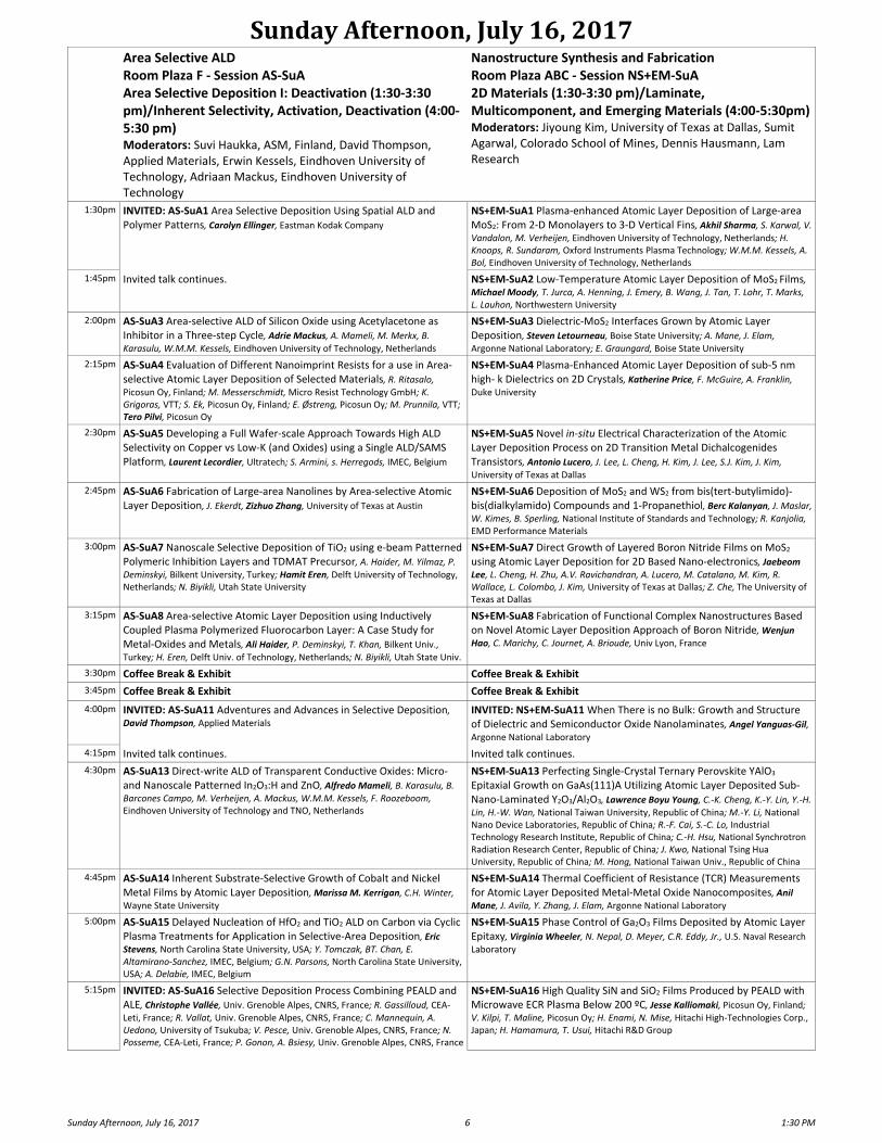
Area Selective ALD Room Plaza F ‐ Session AS‐SuA Area Selective Deposition I: Deactivation (1:30‐3:30 pm)/Inherent Selectivity, Activation, Deactivation (4:00‐5:30 pm) Moderators: Suvi Haukka, ASM, Finland, David Thompson, Applied Materials, Erwin Kessels, Eindhoven University of Technology, Adriaan Mackus, Eindhoven University of Technology
Nanostructure Synthesis and FabricationRoom Plaza ABC ‐ Session NS+EM‐SuA 2D Materials (1:30‐3:30 pm)/Laminate, Multicomponent, and Emerging Materials (4:00‐5:30pm)Moderators: Jiyoung Kim, University of Texas at Dallas, Sumit Agarwal, Colorado School of Mines, Dennis Hausmann, Lam Research
1:30pm INVITED: AS‐SuA1 Area Selective Deposition Using Spatial ALD and Polymer Patterns, Carolyn Ellinger, Eastman Kodak Company
NS+EM‐SuA1 Plasma‐enhanced Atomic Layer Deposition of Large‐area MoS2: From 2‐D Monolayers to 3‐D Vertical Fins, Akhil Sharma, S. Karwal, V.
Vandalon, M. Verheijen, Eindhoven University of Technology, Netherlands; H. Knoops, R. Sundaram, Oxford Instruments Plasma Technology; W.M.M. Kessels, A. Bol, Eindhoven University of Technology, Netherlands
1:45pm Invited talk continues. NS+EM‐SuA2 Low‐Temperature Atomic Layer Deposition of MoS2 Films, Michael Moody, T. Jurca, A. Henning, J. Emery, B. Wang, J. Tan, T. Lohr, T. Marks, L. Lauhon, Northwestern University
2:00pm AS‐SuA3 Area‐selective ALD of Silicon Oxide using Acetylacetone as Inhibitor in a Three‐step Cycle, Adrie Mackus, A. Mameli, M. Merkx, B.
Karasulu, W.M.M. Kessels, Eindhoven University of Technology, Netherlands
NS+EM‐SuA3 Dielectric‐MoS2 Interfaces Grown by Atomic Layer Deposition, Steven Letourneau, Boise State University; A. Mane, J. Elam,
Argonne National Laboratory; E. Graungard, Boise State University
2:15pm AS‐SuA4 Evaluation of Different Nanoimprint Resists for a use in Area‐selective Atomic Layer Deposition of Selected Materials, R. Ritasalo, Picosun Oy, Finland; M. Messerschmidt, Micro Resist Technology GmbH; K. Grigoras, VTT; S. Ek, Picosun Oy, Finland; E. Østreng, Picosun Oy; M. Prunnila, VTT; Tero Pilvi, Picosun Oy
NS+EM‐SuA4 Plasma‐Enhanced Atomic Layer Deposition of sub‐5 nm high‐ k Dielectrics on 2D Crystals, Katherine Price, F. McGuire, A. Franklin,
Duke University
2:30pm AS‐SuA5 Developing a Full Wafer‐scale Approach Towards High ALD Selectivity on Copper vs Low‐K (and Oxides) using a Single ALD/SAMS Platform, Laurent Lecordier, Ultratech; S. Armini, s. Herregods, IMEC, Belgium
NS+EM‐SuA5 Novel in‐situ Electrical Characterization of the Atomic Layer Deposition Process on 2D Transition Metal Dichalcogenides Transistors, Antonio Lucero, J. Lee, L. Cheng, H. Kim, J. Lee, S.J. Kim, J. Kim,
University of Texas at Dallas
2:45pm AS‐SuA6 Fabrication of Large‐area Nanolines by Area‐selective Atomic Layer Deposition, J. Ekerdt, Zizhuo Zhang, University of Texas at Austin
NS+EM‐SuA6 Deposition of MoS2 and WS2 from bis(tert‐butylimido)‐bis(dialkylamido) Compounds and 1‐Propanethiol, Berc Kalanyan, J. Maslar,
W. Kimes, B. Sperling, National Institute of Standards and Technology; R. Kanjolia, EMD Performance Materials
3:00pm AS‐SuA7 Nanoscale Selective Deposition of TiO2 using e‐beam Patterned Polymeric Inhibition Layers and TDMAT Precursor, A. Haider, M. Yilmaz, P.
Deminskyi, Bilkent University, Turkey; Hamit Eren, Delft University of Technology, Netherlands; N. Biyikli, Utah State University
NS+EM‐SuA7 Direct Growth of Layered Boron Nitride Films on MoS2 using Atomic Layer Deposition for 2D Based Nano‐electronics, Jaebeom
Lee, L. Cheng, H. Zhu, A.V. Ravichandran, A. Lucero, M. Catalano, M. Kim, R. Wallace, L. Colombo, J. Kim, University of Texas at Dallas; Z. Che, The University of Texas at Dallas
3:15pm AS‐SuA8 Area‐selective Atomic Layer Deposition using Inductively Coupled Plasma Polymerized Fluorocarbon Layer: A Case Study for Metal‐Oxides and Metals, Ali Haider, P. Deminskyi, T. Khan, Bilkent Univ.,
Turkey; H. Eren, Delft Univ. of Technology, Netherlands; N. Biyikli, Utah State Univ.
NS+EM‐SuA8 Fabrication of Functional Complex Nanostructures Based on Novel Atomic Layer Deposition Approach of Boron Nitride, Wenjun
Hao, C. Marichy, C. Journet, A. Brioude, Univ Lyon, France
3:30pm Coffee Break & Exhibit Coffee Break & Exhibit
3:45pm Coffee Break & Exhibit Coffee Break & Exhibit
4:00pm INVITED: AS‐SuA11 Adventures and Advances in Selective Deposition, David Thompson, Applied Materials
INVITED: NS+EM‐SuA11 When There is no Bulk: Growth and Structure of Dielectric and Semiconductor Oxide Nanolaminates, Angel Yanguas‐Gil, Argonne National Laboratory
4:15pm Invited talk continues. Invited talk continues.
4:30pm AS‐SuA13 Direct‐write ALD of Transparent Conductive Oxides: Micro‐ and Nanoscale Patterned In2O3:H and ZnO, Alfredo Mameli, B. Karasulu, B.
Barcones Campo, M. Verheijen, A. Mackus, W.M.M. Kessels, F. Roozeboom, Eindhoven University of Technology and TNO, Netherlands
NS+EM‐SuA13 Perfecting Single‐Crystal Ternary Perovskite YAlO3 Epitaxial Growth on GaAs(111)A Utilizing Atomic Layer Deposited Sub‐Nano‐Laminated Y2O3/Al2O3, Lawrence Boyu Young, C.‐K. Cheng, K.‐Y. Lin, Y.‐H.
Lin, H.‐W. Wan, National Taiwan University, Republic of China; M.‐Y. Li, National Nano Device Laboratories, Republic of China; R.‐F. Cai, S.‐C. Lo, Industrial Technology Research Institute, Republic of China; C.‐H. Hsu, National Synchrotron Radiation Research Center, Republic of China; J. Kwo, National Tsing Hua University, Republic of China; M. Hong, National Taiwan Univ., Republic of China
4:45pm AS‐SuA14 Inherent Substrate‐Selective Growth of Cobalt and Nickel Metal Films by Atomic Layer Deposition, Marissa M. Kerrigan, C.H. Winter,
Wayne State University
NS+EM‐SuA14 Thermal Coefficient of Resistance (TCR) Measurements for Atomic Layer Deposited Metal‐Metal Oxide Nanocomposites, Anil Mane, J. Avila, Y. Zhang, J. Elam, Argonne National Laboratory
5:00pm AS‐SuA15 Delayed Nucleation of HfO2 and TiO2 ALD on Carbon via Cyclic Plasma Treatments for Application in Selective‐Area Deposition, Eric Stevens, North Carolina State University, USA; Y. Tomczak, BT. Chan, E. Altamirano‐Sanchez, IMEC, Belgium; G.N. Parsons, North Carolina State University, USA; A. Delabie, IMEC, Belgium
NS+EM‐SuA15 Phase Control of Ga2O3 Films Deposited by Atomic Layer Epitaxy, Virginia Wheeler, N. Nepal, D. Meyer, C.R. Eddy, Jr., U.S. Naval Research
Laboratory
5:15pm INVITED: AS‐SuA16 Selective Deposition Process Combining PEALD and ALE, Christophe Vallée, Univ. Grenoble Alpes, CNRS, France; R. Gassilloud, CEA‐Leti, France; R. Vallat, Univ. Grenoble Alpes, CNRS, France; C. Mannequin, A. Uedono, University of Tsukuba; V. Pesce, Univ. Grenoble Alpes, CNRS, France; N. Posseme, CEA‐Leti, France; P. Gonon, A. Bsiesy, Univ. Grenoble Alpes, CNRS, France
NS+EM‐SuA16 High Quality SiN and SiO2 Films Produced by PEALD with Microwave ECR Plasma Below 200 ºC, Jesse Kalliomaki, Picosun Oy, Finland;
V. Kilpi, T. Maline, Picosun Oy; H. Enami, N. Mise, Hitachi High‐Technologies Corp., Japan; H. Hamamura, T. Usui, Hitachi R&D Group
SundayAfternoon,July16,2017
Sunday Afternoon, July 16, 2017 7 1:30 PM
5:30pm Invited talk continues. NS+EM‐SuA17 Tertiary Butyl Hydrazine as a Reducing Agent for Low‐Temperature Atomic Layer Deposition of Low‐Resistivity Copper Thin Films, Katja Väyrynen, K. Mizohata, J. Räisänen, University of Helsinki, Finland; D.
Peeters, A. Devi, Ruhr‐University Bochum, Germany; M. Ritala, M. Leskelä, University of Helsinki, Finland
SundayEveningPosterSessions,July16,2017
Sunday Evening Poster Sessions, July 16, 2017 8 5:30 PM
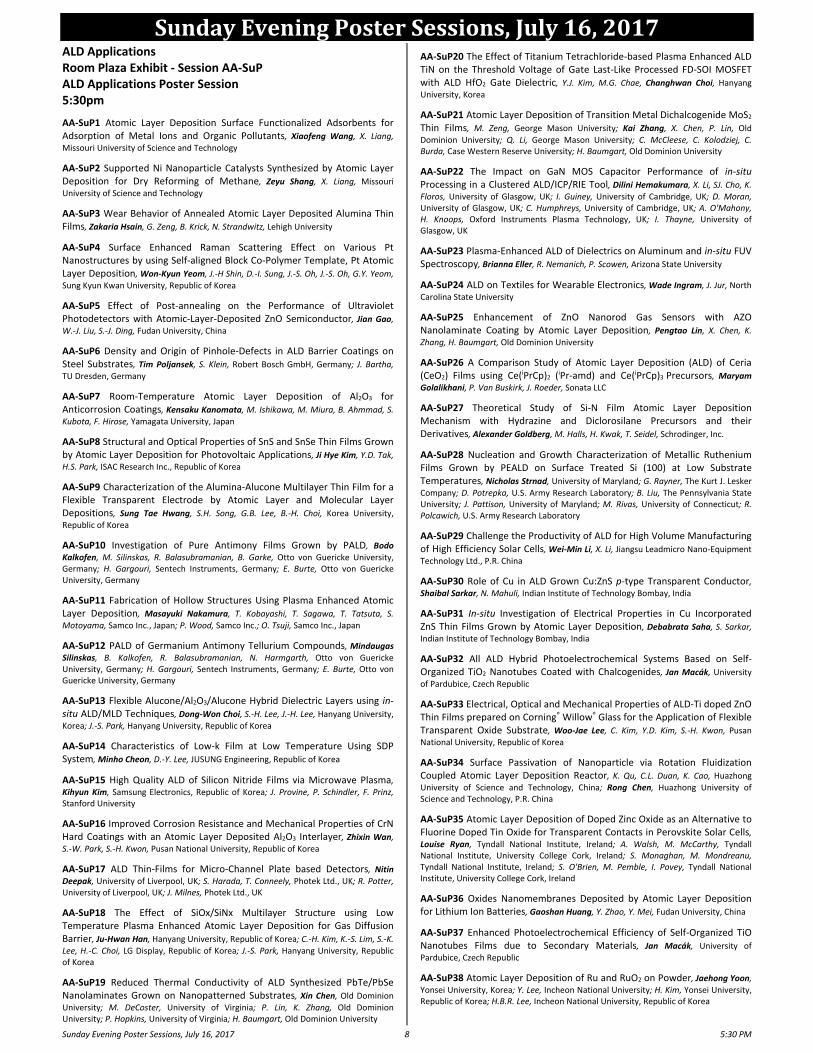
ALD Applications Room Plaza Exhibit ‐ Session AA‐SuP ALD Applications Poster Session 5:30pm
AA‐SuP1 Atomic Layer Deposition Surface Functionalized Adsorbents for Adsorption of Metal Ions and Organic Pollutants, Xiaofeng Wang, X. Liang,
Missouri University of Science and Technology
AA‐SuP2 Supported Ni Nanoparticle Catalysts Synthesized by Atomic Layer Deposition for Dry Reforming of Methane, Zeyu Shang, X. Liang, Missouri
University of Science and Technology
AA‐SuP3 Wear Behavior of Annealed Atomic Layer Deposited Alumina Thin Films, Zakaria Hsain, G. Zeng, B. Krick, N. Strandwitz, Lehigh University
AA‐SuP4 Surface Enhanced Raman Scattering Effect on Various Pt Nanostructures by using Self‐aligned Block Co‐Polymer Template, Pt Atomic Layer Deposition, Won‐Kyun Yeom, J.‐H Shin, D.‐I. Sung, J.‐S. Oh, J.‐S. Oh, G.Y. Yeom,
Sung Kyun Kwan University, Republic of Korea
AA‐SuP5 Effect of Post‐annealing on the Performance of Ultraviolet Photodetectors with Atomic‐Layer‐Deposited ZnO Semiconductor, Jian Gao, W.‐J. Liu, S.‐J. Ding, Fudan University, China
AA‐SuP6 Density and Origin of Pinhole‐Defects in ALD Barrier Coatings on Steel Substrates, Tim Poljansek, S. Klein, Robert Bosch GmbH, Germany; J. Bartha,
TU Dresden, Germany
AA‐SuP7 Room‐Temperature Atomic Layer Deposition of Al2O3 for Anticorrosion Coatings, Kensaku Kanomata, M. Ishikawa, M. Miura, B. Ahmmad, S.
Kubota, F. Hirose, Yamagata University, Japan
AA‐SuP8 Structural and Optical Properties of SnS and SnSe Thin Films Grown by Atomic Layer Deposition for Photovoltaic Applications, Ji Hye Kim, Y.D. Tak,
H.S. Park, ISAC Research Inc., Republic of Korea
AA‐SuP9 Characterization of the Alumina‐Alucone Multilayer Thin Film for a Flexible Transparent Electrode by Atomic Layer and Molecular Layer Depositions, Sung Tae Hwang, S.H. Song, G.B. Lee, B.‐H. Choi, Korea University,
Republic of Korea
AA‐SuP10 Investigation of Pure Antimony Films Grown by PALD, Bodo Kalkofen, M. Silinskas, R. Balasubramanian, B. Garke, Otto von Guericke University, Germany; H. Gargouri, Sentech Instruments, Germany; E. Burte, Otto von Guericke University, Germany
AA‐SuP11 Fabrication of Hollow Structures Using Plasma Enhanced Atomic Layer Deposition, Masayuki Nakamura, T. Kobayashi, T. Sagawa, T. Tatsuta, S.
Motoyama, Samco Inc., Japan; P. Wood, Samco Inc.; O. Tsuji, Samco Inc., Japan
AA‐SuP12 PALD of Germanium Antimony Tellurium Compounds, Mindaugas
Silinskas, B. Kalkofen, R. Balasubramanian, N. Harmgarth, Otto von Guericke University, Germany; H. Gargouri, Sentech Instruments, Germany; E. Burte, Otto von Guericke University, Germany
AA‐SuP13 Flexible Alucone/Al2O3/Alucone Hybrid Dielectric Layers using in‐situ ALD/MLD Techniques, Dong‐Won Choi, S.‐H. Lee, J.‐H. Lee, Hanyang University,
Korea; J.‐S. Park, Hanyang University, Republic of Korea
AA‐SuP14 Characteristics of Low‐k Film at Low Temperature Using SDP System, Minho Cheon, D.‐Y. Lee, JUSUNG Engineering, Republic of Korea
AA‐SuP15 High Quality ALD of Silicon Nitride Films via Microwave Plasma, Kihyun Kim, Samsung Electronics, Republic of Korea; J. Provine, P. Schindler, F. Prinz, Stanford University
AA‐SuP16 Improved Corrosion Resistance and Mechanical Properties of CrN Hard Coatings with an Atomic Layer Deposited Al2O3 Interlayer, Zhixin Wan,
S.‐W. Park, S.‐H. Kwon, Pusan National University, Republic of Korea
AA‐SuP17 ALD Thin‐Films for Micro‐Channel Plate based Detectors, Nitin Deepak, University of Liverpool, UK; S. Harada, T. Conneely, Photek Ltd., UK; R. Potter, University of Liverpool, UK; J. Milnes, Photek Ltd., UK
AA‐SuP18 The Effect of SiOx/SiNx Multilayer Structure using Low Temperature Plasma Enhanced Atomic Layer Deposition for Gas Diffusion Barrier, Ju‐Hwan Han, Hanyang University, Republic of Korea; C.‐H. Kim, K.‐S. Lim, S.‐K.
Lee, H.‐C. Choi, LG Display, Republic of Korea; J.‐S. Park, Hanyang University, Republic of Korea
AA‐SuP19 Reduced Thermal Conductivity of ALD Synthesized PbTe/PbSe Nanolaminates Grown on Nanopatterned Substrates, Xin Chen, Old Dominion
University; M. DeCoster, University of Virginia; P. Lin, K. Zhang, Old Dominion University; P. Hopkins, University of Virginia; H. Baumgart, Old Dominion University
AA‐SuP20 The Effect of Titanium Tetrachloride‐based Plasma Enhanced ALD TiN on the Threshold Voltage of Gate Last‐Like Processed FD‐SOI MOSFET with ALD HfO2 Gate Dielectric, Y.J. Kim, M.G. Chae, Changhwan Choi, Hanyang
University, Korea
AA‐SuP21 Atomic Layer Deposition of Transition Metal Dichalcogenide MoS2 Thin Films, M. Zeng, George Mason University; Kai Zhang, X. Chen, P. Lin, Old
Dominion University; Q. Li, George Mason University; C. McCleese, C. Kolodziej, C. Burda, Case Western Reserve University; H. Baumgart, Old Dominion University
AA‐SuP22 The Impact on GaN MOS Capacitor Performance of in‐situ Processing in a Clustered ALD/ICP/RIE Tool, Dilini Hemakumara, X. Li, SJ. Cho, K.
Floros, University of Glasgow, UK; I. Guiney, University of Cambridge, UK; D. Moran, University of Glasgow, UK; C. Humphreys, University of Cambridge, UK; A. O'Mahony, H. Knoops, Oxford Instruments Plasma Technology, UK; I. Thayne, University of Glasgow, UK
AA‐SuP23 Plasma‐Enhanced ALD of Dielectrics on Aluminum and in‐situ FUV Spectroscopy, Brianna Eller, R. Nemanich, P. Scowen, Arizona State University
AA‐SuP24 ALD on Textiles for Wearable Electronics, Wade Ingram, J. Jur, North
Carolina State University
AA‐SuP25 Enhancement of ZnO Nanorod Gas Sensors with AZO Nanolaminate Coating by Atomic Layer Deposition, Pengtao Lin, X. Chen, K. Zhang, H. Baumgart, Old Dominion University
AA‐SuP26 A Comparison Study of Atomic Layer Deposition (ALD) of Ceria (CeO2) Films using Ce(iPrCp)2 (iPr‐amd) and Ce(iPrCp)3 Precursors, Maryam
Golalikhani, P. Van Buskirk, J. Roeder, Sonata LLC
AA‐SuP27 Theoretical Study of Si‐N Film Atomic Layer Deposition Mechanism with Hydrazine and Diclorosilane Precursors and their Derivatives, Alexander Goldberg, M. Halls, H. Kwak, T. Seidel, Schrodinger, Inc.
AA‐SuP28 Nucleation and Growth Characterization of Metallic Ruthenium Films Grown by PEALD on Surface Treated Si (100) at Low Substrate Temperatures, Nicholas Strnad, University of Maryland; G. Rayner, The Kurt J. Lesker
Company; D. Potrepka, U.S. Army Research Laboratory; B. Liu, The Pennsylvania State University; J. Pattison, University of Maryland; M. Rivas, University of Connecticut; R. Polcawich, U.S. Army Research Laboratory
AA‐SuP29 Challenge the Productivity of ALD for High Volume Manufacturing of High Efficiency Solar Cells, Wei‐Min Li, X. Li, Jiangsu Leadmicro Nano‐Equipment
Technology Ltd., P.R. China
AA‐SuP30 Role of Cu in ALD Grown Cu:ZnS p‐type Transparent Conductor, Shaibal Sarkar, N. Mahuli, Indian Institute of Technology Bombay, India
AA‐SuP31 In‐situ Investigation of Electrical Properties in Cu Incorporated ZnS Thin Films Grown by Atomic Layer Deposition, Debabrata Saha, S. Sarkar, Indian Institute of Technology Bombay, India
AA‐SuP32 All ALD Hybrid Photoelectrochemical Systems Based on Self‐Organized TiO2 Nanotubes Coated with Chalcogenides, Jan Macák, University
of Pardubice, Czech Republic
AA‐SuP33 Electrical, Optical and Mechanical Properties of ALD‐Ti doped ZnO Thin Films prepared on Corning® Willow® Glass for the Application of Flexible Transparent Oxide Substrate, Woo‐Jae Lee, C. Kim, Y.D. Kim, S.‐H. Kwon, Pusan
National University, Republic of Korea
AA‐SuP34 Surface Passivation of Nanoparticle via Rotation Fluidization Coupled Atomic Layer Deposition Reactor, K. Qu, C.L. Duan, K. Cao, Huazhong University of Science and Technology, China; Rong Chen, Huazhong University of Science and Technology, P.R. China
AA‐SuP35 Atomic Layer Deposition of Doped Zinc Oxide as an Alternative to Fluorine Doped Tin Oxide for Transparent Contacts in Perovskite Solar Cells, Louise Ryan, Tyndall National Institute, Ireland; A. Walsh, M. McCarthy, Tyndall National Institute, University College Cork, Ireland; S. Monaghan, M. Mondreanu, Tyndall National Institute, Ireland; S. O'Brien, M. Pemble, I. Povey, Tyndall National Institute, University College Cork, Ireland
AA‐SuP36 Oxides Nanomembranes Deposited by Atomic Layer Deposition for Lithium Ion Batteries, Gaoshan Huang, Y. Zhao, Y. Mei, Fudan University, China
AA‐SuP37 Enhanced Photoelectrochemical Efficiency of Self‐Organized TiO Nanotubes Films due to Secondary Materials, Jan Macák, University of
Pardubice, Czech Republic
AA‐SuP38 Atomic Layer Deposition of Ru and RuO2 on Powder, Jaehong Yoon, Yonsei University, Korea; Y. Lee, Incheon National University; H. Kim, Yonsei University, Republic of Korea; H.B.R. Lee, Incheon National University, Republic of Korea
SundayEveningPosterSessions,July16,2017
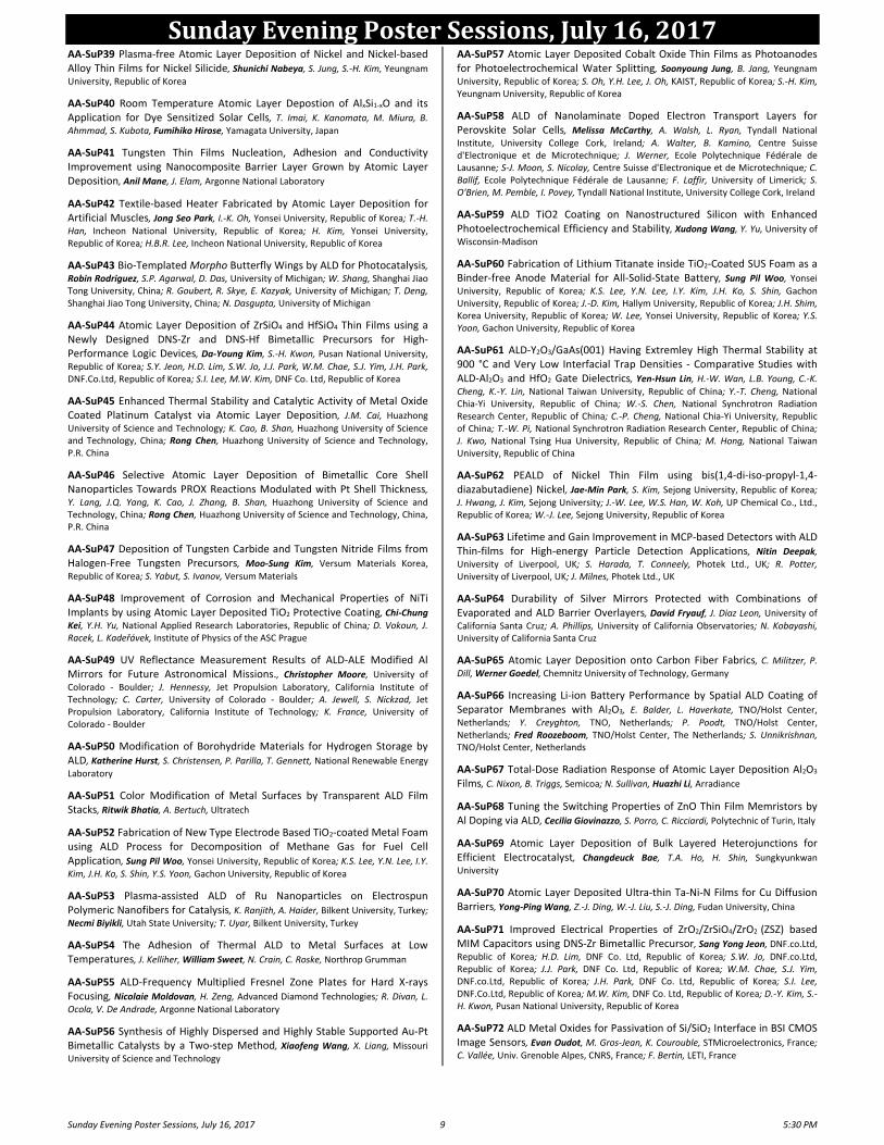
Sunday Evening Poster Sessions, July 16, 2017 9 5:30 PM
AA‐SuP39 Plasma‐free Atomic Layer Deposition of Nickel and Nickel‐based Alloy Thin Films for Nickel Silicide, Shunichi Nabeya, S. Jung, S.‐H. Kim, Yeungnam
University, Republic of Korea
AA‐SuP40 Room Temperature Atomic Layer Depostion of AlxSi1‐xO and its Application for Dye Sensitized Solar Cells, T. Imai, K. Kanomata, M. Miura, B.
Ahmmad, S. Kubota, Fumihiko Hirose, Yamagata University, Japan
AA‐SuP41 Tungsten Thin Films Nucleation, Adhesion and Conductivity Improvement using Nanocomposite Barrier Layer Grown by Atomic Layer Deposition, Anil Mane, J. Elam, Argonne National Laboratory
AA‐SuP42 Textile‐based Heater Fabricated by Atomic Layer Deposition for Artificial Muscles, Jong Seo Park, I.‐K. Oh, Yonsei University, Republic of Korea; T.‐H. Han, Incheon National University, Republic of Korea; H. Kim, Yonsei University, Republic of Korea; H.B.R. Lee, Incheon National University, Republic of Korea
AA‐SuP43 Bio‐Templated Morpho Butterfly Wings by ALD for Photocatalysis, Robin Rodriguez, S.P. Agarwal, D. Das, University of Michigan; W. Shang, Shanghai Jiao Tong University, China; R. Goubert, R. Skye, E. Kazyak, University of Michigan; T. Deng, Shanghai Jiao Tong University, China; N. Dasgupta, University of Michigan
AA‐SuP44 Atomic Layer Deposition of ZrSiO4 and HfSiO4 Thin Films using a Newly Designed DNS‐Zr and DNS‐Hf Bimetallic Precursors for High‐Performance Logic Devices, Da‐Young Kim, S.‐H. Kwon, Pusan National University,
Republic of Korea; S.Y. Jeon, H.D. Lim, S.W. Jo, J.J. Park, W.M. Chae, S.J. Yim, J.H. Park, DNF.Co.Ltd, Republic of Korea; S.I. Lee, M.W. Kim, DNF Co. Ltd, Republic of Korea
AA‐SuP45 Enhanced Thermal Stability and Catalytic Activity of Metal Oxide Coated Platinum Catalyst via Atomic Layer Deposition, J.M. Cai, Huazhong
University of Science and Technology; K. Cao, B. Shan, Huazhong University of Science and Technology, China; Rong Chen, Huazhong University of Science and Technology, P.R. China
AA‐SuP46 Selective Atomic Layer Deposition of Bimetallic Core Shell Nanoparticles Towards PROX Reactions Modulated with Pt Shell Thickness, Y. Lang, J.Q. Yang, K. Cao, J. Zhang, B. Shan, Huazhong University of Science and Technology, China; Rong Chen, Huazhong University of Science and Technology, China, P.R. China
AA‐SuP47 Deposition of Tungsten Carbide and Tungsten Nitride Films from Halogen‐Free Tungsten Precursors, Moo‐Sung Kim, Versum Materials Korea,
Republic of Korea; S. Yabut, S. Ivanov, Versum Materials
AA‐SuP48 Improvement of Corrosion and Mechanical Properties of NiTi Implants by using Atomic Layer Deposited TiO2 Protective Coating, Chi‐Chung Kei, Y.H. Yu, National Applied Research Laboratories, Republic of China; D. Vokoun, J. Racek, L. Kadeřávek, Institute of Physics of the ASC Prague
AA‐SuP49 UV Reflectance Measurement Results of ALD‐ALE Modified Al Mirrors for Future Astronomical Missions., Christopher Moore, University of
Colorado ‐ Boulder; J. Hennessy, Jet Propulsion Laboratory, California Institute of Technology; C. Carter, University of Colorado ‐ Boulder; A. Jewell, S. Nickzad, Jet Propulsion Laboratory, California Institute of Technology; K. France, University of Colorado ‐ Boulder
AA‐SuP50 Modification of Borohydride Materials for Hydrogen Storage by ALD, Katherine Hurst, S. Christensen, P. Parilla, T. Gennett, National Renewable Energy Laboratory
AA‐SuP51 Color Modification of Metal Surfaces by Transparent ALD Film Stacks, Ritwik Bhatia, A. Bertuch, Ultratech
AA‐SuP52 Fabrication of New Type Electrode Based TiO2‐coated Metal Foam using ALD Process for Decomposition of Methane Gas for Fuel Cell Application, Sung Pil Woo, Yonsei University, Republic of Korea; K.S. Lee, Y.N. Lee, I.Y.
Kim, J.H. Ko, S. Shin, Y.S. Yoon, Gachon University, Republic of Korea
AA‐SuP53 Plasma‐assisted ALD of Ru Nanoparticles on Electrospun Polymeric Nanofibers for Catalysis, K. Ranjith, A. Haider, Bilkent University, Turkey; Necmi Biyikli, Utah State University; T. Uyar, Bilkent University, Turkey
AA‐SuP54 The Adhesion of Thermal ALD to Metal Surfaces at Low Temperatures, J. Kelliher, William Sweet, N. Crain, C. Roske, Northrop Grumman
AA‐SuP55 ALD‐Frequency Multiplied Fresnel Zone Plates for Hard X‐rays Focusing, Nicolaie Moldovan, H. Zeng, Advanced Diamond Technologies; R. Divan, L.
Ocola, V. De Andrade, Argonne National Laboratory
AA‐SuP56 Synthesis of Highly Dispersed and Highly Stable Supported Au‐Pt Bimetallic Catalysts by a Two‐step Method, Xiaofeng Wang, X. Liang, Missouri
University of Science and Technology
AA‐SuP57 Atomic Layer Deposited Cobalt Oxide Thin Films as Photoanodes for Photoelectrochemical Water Splitting, Soonyoung Jung, B. Jang, Yeungnam
University, Republic of Korea; S. Oh, Y.H. Lee, J. Oh, KAIST, Republic of Korea; S.‐H. Kim, Yeungnam University, Republic of Korea
AA‐SuP58 ALD of Nanolaminate Doped Electron Transport Layers for Perovskite Solar Cells, Melissa McCarthy, A. Walsh, L. Ryan, Tyndall National
Institute, University College Cork, Ireland; A. Walter, B. Kamino, Centre Suisse d'Electronique et de Microtechnique; J. Werner, Ecole Polytechnique Fédérale de Lausanne; S‐J. Moon, S. Nicolay, Centre Suisse d'Electronique et de Microtechnique; C. Ballif, Ecole Polytechnique Fédérale de Lausanne; F. Laffir, University of Limerick; S. O'Brien, M. Pemble, I. Povey, Tyndall National Institute, University College Cork, Ireland
AA‐SuP59 ALD TiO2 Coating on Nanostructured Silicon with Enhanced Photoelectrochemical Efficiency and Stability, Xudong Wang, Y. Yu, University of
Wisconsin‐Madison
AA‐SuP60 Fabrication of Lithium Titanate inside TiO2‐Coated SUS Foam as a Binder‐free Anode Material for All‐Solid‐State Battery, Sung Pil Woo, Yonsei
University, Republic of Korea; K.S. Lee, Y.N. Lee, I.Y. Kim, J.H. Ko, S. Shin, Gachon University, Republic of Korea; J.‐D. Kim, Hallym University, Republic of Korea; J.H. Shim, Korea University, Republic of Korea; W. Lee, Yonsei University, Republic of Korea; Y.S. Yoon, Gachon University, Republic of Korea
AA‐SuP61 ALD‐Y2O3/GaAs(001) Having Extremley High Thermal Stability at 900 °C and Very Low Interfacial Trap Densities ‐ Comparative Studies with ALD‐Al2O3 and HfO2 Gate Dielectrics, Yen‐Hsun Lin, H.‐W. Wan, L.B. Young, C.‐K.
Cheng, K.‐Y. Lin, National Taiwan University, Republic of China; Y.‐T. Cheng, National Chia‐Yi University, Republic of China; W.‐S. Chen, National Synchrotron Radiation Research Center, Republic of China; C.‐P. Cheng, National Chia‐Yi University, Republic of China; T.‐W. Pi, National Synchrotron Radiation Research Center, Republic of China; J. Kwo, National Tsing Hua University, Republic of China; M. Hong, National Taiwan University, Republic of China
AA‐SuP62 PEALD of Nickel Thin Film using bis(1,4‐di‐iso‐propyl‐1,4‐diazabutadiene) Nickel, Jae‐Min Park, S. Kim, Sejong University, Republic of Korea;
J. Hwang, J. Kim, Sejong University; J.‐W. Lee, W.S. Han, W. Koh, UP Chemical Co., Ltd., Republic of Korea; W.‐J. Lee, Sejong University, Republic of Korea
AA‐SuP63 Lifetime and Gain Improvement in MCP‐based Detectors with ALD Thin‐films for High‐energy Particle Detection Applications, Nitin Deepak, University of Liverpool, UK; S. Harada, T. Conneely, Photek Ltd., UK; R. Potter, University of Liverpool, UK; J. Milnes, Photek Ltd., UK
AA‐SuP64 Durability of Silver Mirrors Protected with Combinations of Evaporated and ALD Barrier Overlayers, David Fryauf, J. Diaz Leon, University of California Santa Cruz; A. Phillips, University of California Observatories; N. Kobayashi, University of California Santa Cruz
AA‐SuP65 Atomic Layer Deposition onto Carbon Fiber Fabrics, C. Militzer, P.
Dill, Werner Goedel, Chemnitz University of Technology, Germany
AA‐SuP66 Increasing Li‐ion Battery Performance by Spatial ALD Coating of Separator Membranes with Al2O3, E. Balder, L. Haverkate, TNO/Holst Center,
Netherlands; Y. Creyghton, TNO, Netherlands; P. Poodt, TNO/Holst Center, Netherlands; Fred Roozeboom, TNO/Holst Center, The Netherlands; S. Unnikrishnan, TNO/Holst Center, Netherlands
AA‐SuP67 Total‐Dose Radiation Response of Atomic Layer Deposition Al2O3 Films, C. Nixon, B. Triggs, Semicoa; N. Sullivan, Huazhi Li, Arradiance
AA‐SuP68 Tuning the Switching Properties of ZnO Thin Film Memristors by Al Doping via ALD, Cecilia Giovinazzo, S. Porro, C. Ricciardi, Polytechnic of Turin, Italy
AA‐SuP69 Atomic Layer Deposition of Bulk Layered Heterojunctions for Efficient Electrocatalyst, Changdeuck Bae, T.A. Ho, H. Shin, Sungkyunkwan
University
AA‐SuP70 Atomic Layer Deposited Ultra‐thin Ta‐Ni‐N Films for Cu Diffusion Barriers, Yong‐Ping Wang, Z.‐J. Ding, W.‐J. Liu, S.‐J. Ding, Fudan University, China
AA‐SuP71 Improved Electrical Properties of ZrO2/ZrSiO4/ZrO2 (ZSZ) based MIM Capacitors using DNS‐Zr Bimetallic Precursor, Sang Yong Jeon, DNF.co.Ltd, Republic of Korea; H.D. Lim, DNF Co. Ltd, Republic of Korea; S.W. Jo, DNF.co.Ltd, Republic of Korea; J.J. Park, DNF Co. Ltd, Republic of Korea; W.M. Chae, S.J. Yim, DNF.co.Ltd, Republic of Korea; J.H. Park, DNF Co. Ltd, Republic of Korea; S.I. Lee, DNF.Co.Ltd, Republic of Korea; M.W. Kim, DNF Co. Ltd, Republic of Korea; D.‐Y. Kim, S.‐H. Kwon, Pusan National University, Republic of Korea
AA‐SuP72 ALD Metal Oxides for Passivation of Si/SiO2 Interface in BSI CMOS Image Sensors, Evan Oudot, M. Gros‐Jean, K. Courouble, STMicroelectronics, France;
C. Vallée, Univ. Grenoble Alpes, CNRS, France; F. Bertin, LETI, France
SundayEveningPosterSessions,July16,2017
Sunday Evening Poster Sessions, July 16, 2017 10 5:30 PM
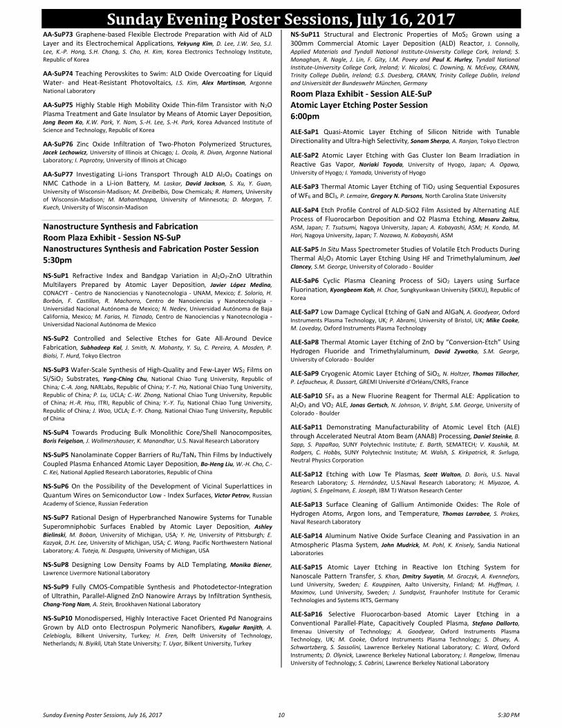
AA‐SuP73 Graphene‐based Flexible Electrode Preparation with Aid of ALD Layer and its Electrochemical Applications, Yekyung Kim, D. Lee, J.W. Seo, S.J.
Lee, K.‐P. Hong, S.H. Chang, S. Cho, H. Kim, Korea Electronics Technology Institute, Republic of Korea
AA‐SuP74 Teaching Perovskites to Swim: ALD Oxide Overcoating for Liquid Water‐ and Heat‐Resistant Photovoltaics, I.S. Kim, Alex Martinson, Argonne
National Laboratory
AA‐SuP75 Highly Stable High Mobility Oxide Thin‐film Transistor with N2O Plasma Treatment and Gate Insulator by Means of Atomic Layer Deposition, Jong Beom Ko, K.W. Park, Y. Nam, S.‐H. Lee, S.‐H. Park, Korea Advanced Institute of Science and Technology, Republic of Korea
AA‐SuP76 Zinc Oxide Infiltration of Two‐Photon Polymerized Structures, Jacek Lechowicz, University of Illinois at Chicago; L. Ocola, R. Divan, Argonne National Laboratory; I. Paprotny, University of Illinois at Chicago
AA‐SuP77 Investigating Li‐ions Transport Through ALD Al2O3 Coatings on NMC Cathode in a Li‐ion Battery, M. Laskar, David Jackson, S. Xu, Y. Guan,
University of Wisconsin‐Madison; M. Dreibelbis, Dow Chemicals; R. Hamers, University of Wisconsin‐Madison; M. Mahanthappa, University of Minnesota; D. Morgan, T. Kuech, University of Wisconsin‐Madison
Nanostructure Synthesis and Fabrication Room Plaza Exhibit ‐ Session NS‐SuP Nanostructures Synthesis and Fabrication Poster Session 5:30pm
NS‐SuP1 Refractive Index and Bandgap Variation in Al2O3‐ZnO Ultrathin Multilayers Prepared by Atomic Layer Deposition, Javier López Medina,
CONACYT ‐ Centro de Nanociencias y Nanotecnologia ‐ UNAM, Mexico; E. Solorio, H. Borbón, F. Castillon, R. Machorro, Centro de Nanociencias y Nanotecnologia ‐ Universidad Nacional Autónoma de Mexico; N. Nedev, Universidad Autónoma de Baja California, Mexico; M. Farias, H. Tiznado, Centro de Nanociencias y Nanotecnologia ‐ Universidad Nacional Autónoma de Mexico
NS‐SuP2 Controlled and Selective Etches for Gate All‐Around Device Fabrication, Subhadeep Kal, J. Smith, N. Mohanty, Y. Su, C. Pereira, A. Mosden, P.
Biolsi, T. Hurd, Tokyo Electron
NS‐SuP3 Wafer‐Scale Synthesis of High‐Quality and Few‐Layer WS2 Films on Si/SiO2 Substrates, Yung‐Ching Chu, National Chiao Tung University, Republic of China; C.‐A. Jong, NARLabs, Republic of China; Y.‐T. Ho, National Chiao Tung University, Republic of China; P. Lu, UCLA; C.‐W. Zhong, National Chiao Tung University, Republic of China; H.‐R. Hsu, ITRI, Republic of China; Y.‐Y. Tu, National Chiao Tung University, Republic of China; J. Woo, UCLA; E.‐Y. Chang, National Chiao Tung University, Republic of China
NS‐SuP4 Towards Producing Bulk Monolithic Core/Shell Nanocomposites, Boris Feigelson, J. Wollmershauser, K. Manandhar, U.S. Naval Research Laboratory
NS‐SuP5 Nanolaminate Copper Barriers of Ru/TaNx Thin Films by Inductively Coupled Plasma Enhanced Atomic Layer Deposition, Bo‐Heng Liu, W.‐H. Cho, C.‐
C. Kei, National Applied Research Laboratories, Republic of China
NS‐SuP6 On the Possibility of the Development of Vicinal Superlattices in Quantum Wires on Semiconductor Low ‐ Index Surfaces, Victor Petrov, Russian Academy of Science, Russian Federation
NS‐SuP7 Rational Design of Hyperbranched Nanowire Systems for Tunable Superomniphobic Surfaces Enabled by Atomic Layer Deposition, Ashley Bielinski, M. Boban, University of Michigan, USA; Y. He, University of Pittsburgh; E. Kazyak, D.H. Lee, University of Michigan, USA; C. Wang, Pacific Northwestern National Laboratory; A. Tuteja, N. Dasgupta, University of Michigan, USA
NS‐SuP8 Designing Low Density Foams by ALD Templating, Monika Biener,
Lawrence Livermore National Laboratory
NS‐SuP9 Fully CMOS‐Compatible Synthesis and Photodetector‐Integration of Ultrathin, Parallel‐Aligned ZnO Nanowire Arrays by Infiltration Synthesis, Chang‐Yong Nam, A. Stein, Brookhaven National Laboratory
NS‐SuP10 Monodispersed, Highly Interactive Facet Oriented Pd Nanograins Grown by ALD onto Electrospun Polymeric Nanofibers, Kugalur Ranjith, A. Celebioglu, Bilkent University, Turkey; H. Eren, Delft University of Technology, Netherlands; N. Biyikli, Utah State University; T. Uyar, Bilkent University, Turkey
NS‐SuP11 Structural and Electronic Properties of MoS2 Grown using a 300mm Commercial Atomic Layer Deposition (ALD) Reactor, J. Connolly, Applied Materials and Tyndall National Institute‐University College Cork, Ireland; S. Monaghan, R. Nagle, J. Lin, F. Gity, I.M. Povey and Paul K. Hurley, Tyndall National Institute‐University College Cork, Ireland; V. Nicolosi, C. Downing, N. McEvoy, CRANN, Trinity College Dublin, Ireland; G.S. Duesberg, CRANN, Trinity College Dublin, Ireland and Universität der Bundeswehr München, Germany
Room Plaza Exhibit ‐ Session ALE‐SuP Atomic Layer Etching Poster Session 6:00pm
ALE‐SaP1 Quasi‐Atomic Layer Etching of Silicon Nitride with Tunable Directionality and Ultra‐high Selectivity, Sonam Sherpa, A. Ranjan, Tokyo Electron
ALE‐SaP2 Atomic Layer Etching with Gas Cluster Ion Beam Irradiation in Reactive Gas Vapor, Noriaki Toyoda, University of Hyogo, Japan; A. Ogawa, University of Hyogo; I. Yamada, Univeristy of Hyogo
ALE‐SaP3 Thermal Atomic Layer Etching of TiO2 using Sequential Exposures of WF6 and BCl3, P. Lemaire, Gregory N. Parsons, North Carolina State University
ALE‐SaP4 Etch Profile Control of ALD‐SiO2 Film Assisted by Alternating ALE Process of Fluorocarbon Deposition and O2 Plasma Etching, Masaru Zaitsu,
ASM, Japan; T. Tsutsumi, Nagoya University, Japan; A. Kobayashi, ASM; H. Kondo, M. Hori, Nagoya University, Japan; T. Nozawa, N. Kobayashi, ASM
ALE‐SaP5 In Situ Mass Spectrometer Studies of Volatile Etch Products During Thermal Al2O3 Atomic Layer Etching Using HF and Trimethylaluminum, Joel
Clancey, S.M. George, University of Colorado ‐ Boulder
ALE‐SaP6 Cyclic Plasma Cleaning Process of SiO2 Layers using Surface Fluorination, Kyongbeom Koh, H. Chae, Sungkyunkwan University (SKKU), Republic of
Korea
ALE‐SaP7 Low Damage Cyclical Etching of GaN and AlGaN, A. Goodyear, Oxford Instruments Plasma Technology, UK; P. Abrami, University of Bristol, UK; Mike Cooke, M. Loveday, Oxford Instruments Plasma Technology
ALE‐SaP8 Thermal Atomic Layer Etching of ZnO by “Conversion‐Etch” Using Hydrogen Fluoride and Trimethylaluminum, David Zywotko, S.M. George,
University of Colorado ‐ Boulder
ALE‐SaP9 Cryogenic Atomic Layer Etching of SiO2, N. Holtzer, Thomas Tillocher,
P. Lefaucheux, R. Dussart, GREMI Université d'Orléans/CNRS, France
ALE‐SaP10 SF4 as a New Fluorine Reagent for Thermal ALE: Application to Al2O3 and VO2 ALE, Jonas Gertsch, N. Johnson, V. Bright, S.M. George, University of
Colorado ‐ Boulder
ALE‐SaP11 Demonstrating Manufacturability of Atomic Level Etch (ALE) through Accelerated Neutral Atom Beam (ANAB) Processing, Daniel Steinke, B. Sapp, S. PapaRao, SUNY Polytechnic Institute; E. Barth, SEMATECH; V. Kaushik, M. Rodgers, C. Hobbs, SUNY Polytechnic Institute; M. Walsh, S. Kirkpatrick, R. Svrluga, Neutral Physics Corporation
ALE‐SaP12 Etching with Low Te Plasmas, Scott Walton, D. Boris, U.S. Naval
Research Laboratory; S. Hernández, U.S.Naval Research Laboratory; H. Miyazoe, A. Jagtiani, S. Engelmann, E. Joseph, IBM TJ Watson Research Center
ALE‐SaP13 Surface Cleaning of Gallium Antimonide Oxides: The Role of Hydrogen Atoms, Argon Ions, and Temperature, Thomas Larrabee, S. Prokes,
Naval Research Laboratory
ALE‐SaP14 Aluminum Native Oxide Surface Cleaning and Passivation in an Atmospheric Plasma System, John Mudrick, M. Pohl, K. Knisely, Sandia National
Laboratories
ALE‐SaP15 Atomic Layer Etching in Reactive Ion Etching System for Nanoscale Pattern Transfer, S. Khan, Dmitry Suyatin, M. Graczyk, A. Kvennefors,
Lund University, Sweden; E. Kauppinen, Aalto University, Finland; M. Huffman, I. Maximov, Lund University, Sweden; J. Sundqvist, Fraunhofer Institute for Ceramic Technologies and Systems IKTS, Germany
ALE‐SaP16 Selective Fluorocarbon‐based Atomic Layer Etching in a Conventional Parallel‐Plate, Capacitively Coupled Plasma, Stefano Dallorto, Ilmenau University of Technology; A. Goodyear, Oxford Instruments Plasma Technology, UK; M. Cooke, Oxford Instruments Plasma Technology; S. Dhuey, A. Schwartzberg, S. Sassolini, Lawrence Berkeley National Laboratory; C. Ward, Oxford Instruments; D. Olynick, Lawrence Berkeley National Laboratory; I. Rangelow, Ilmenau University of Technology; S. Cabrini, Lawrence Berkeley National Laboratory
SundayEveningPosterSessions,July16,2017
Sunday Evening Poster Sessions, July 16, 2017 11 5:30 PM
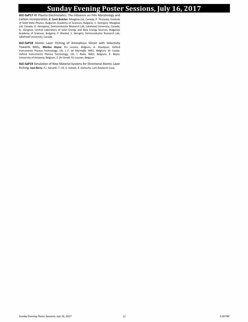
ALE‐SaP17 RF Plasma Electrostatics: The Influence on Film Morphology and Carbon Incorporation, K. Scott Butcher, Meaglow Ltd, Canada; P. Terziyska, Institute
of Solid State Physics, Bulgarian Academy of Sciences, Bulgaria; V. Georgiev, Meaglow Ltd, Canada; D. Georgieva, Semiconductor Research Lab, Lakehead University, Canada; R,. Gergova, Central Laboratory of Solar Energy and New Energy Sources, Bulgarian Academy of Sciences, Bulgaria; P. Binsted, S. Skergetc, Semiconductor Research Lab, Lakehead University, Canada
ALE‐SaP18 Atomic Layer Etching of Amorphous Silicon with Selectivity Towards MoS2, Markus Heyne, KU Leuven, Belgium; A. Goodyear, Oxford
Instruments Plasma Technology, UK; J.‐F. de Marneffe, IMEC, Belgium; M. Cooke, Oxford Instruments Plasma Technology, UK; I. Radu, IMEC, Belgium; E. Neyts, University of Antwerp, Belgium; S. De Gendt, KU Leuven, Belgium
ALE‐SaP19 Simulation of New Material‐Systems for Directional Atomic Layer Etching, Ivan Berry, K.J. Kanarik, T. Lill, V. Vahedi, R. Gottscho, Lam Research Corp.
MondayMorning,July17,2017
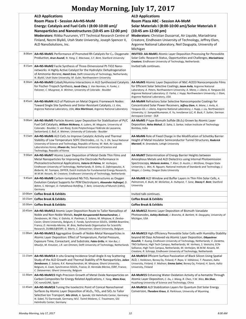
Monday Morning, July 17, 2017 12 8:00 AM
ALD Applications Room Plaza E ‐ Session AA+NS‐MoM Energy: Catalysis and Fuel Cells I (8:00‐10:00 am)/ Nanoparticles and Nanostructures (10:45 am‐12:00 pm) Moderators: Riikka Puurunen, VTT Technical Research Centre of Finland, Necmi Biyikli, Utah State University, Joseph Spencer II, ALD NanoSolutions, Inc.
ALD ApplicationsRoom Plaza ABC ‐ Session AA‐MoM Solar Materials I (8:00‐10:00 am)/Solar Materials II (10:45 am‐12:00 pm) Moderators: Christian Dussarrat, Air Liquide, Mariadriana Creatore, Eindhoven University of Technology, Jeffrey Elam, Argonne National Laboratory, Neil Dasgupta, University of Michigan
8:00am AA+NS‐MoM1 Performance of Promoted Rh Catalysts for C2+ Oxygenate Production, Arun Asundi, N. Yang, C. MacIsaac, S.F. Bent, Stanford University
INVITED: AA‐MoM1 Atomic Layer Deposition Processing for Perovskite Solar Cells: Research Status, Opportunities and Challenges, Mariadriana
Creatore, Eindhoven University of Technology, Netherlands
8:15am AA+NS‐MoM2 Facile Synthesis of Three‐Dimensional Pt‐TiO2 Nano‐networks: A Highly Active Catalyst for the Hydrolytic Dehydrogenation of Ammonia–Borane, Hamit Eren, Delft University of Technology, Netherlands;
N. Biyikli, Utah State University; M. Guler, Northwestern University
Invited talk continues.
8:30am AA+NS‐MoM3 Cobalt/Alumina Interactions in ALD Synthesized Catalysts for Fischer‐Tropsch Synthesis, Jacob Clary, S. Van Norman, H. Funke, J.
Falconer, C. Musgrave, A. Weimer, University of Colorado ‐ Boulder
AA‐MoM3 Atomic Layer Deposition of NbC‐Al2O3 Nanocomposite Films for Efficient Solar Selective Coatings, Jason Avila, Argonne National Laboratory; A. Peters, Northwestern University; A. Mane, J. Libera, A. Yanguas‐Gil, Argonne National Laboratory; O. Farha, J. Hupp, Northwestern University; J. Elam, Argonne National Laboratory, USA
8:45am AA+NS‐MoM4 ALD of Platinum on Metal Organic Framework Nodes: Toward Single Site Synthesis and Sinter‐Resistant Catalysts, I.S. Kim,
Argonne National Laboratory, USA; Alex Martinson, Argonne National Laboratory
AA‐MoM4 Refractory Solar Selective Nanocomposite Coatings for Concentrated Solar Power Receivers, Jeffrey Elam, A. Mane, J. Avila, A.
Yanguas‐Gil, J. Libera, Argonne National Laboratory; J. Hupp, J. Liu, Northwestern University; U. Sampathkumaran, K. Yu, InnoSense LLC; R. Buck, F. Sutter, German Aerospace Center ‐ DLR
9:00am AA+NS‐MoM5 Particle Atomic Layer Deposition for Stabilization of Pt/C Fuel Cell Catalysts, William McNeary, A. Lubers, M. Maguire, University of
Colorado ‐ Boulder; S. van Rooij, Ecole Polytechnique Fédérale de Lausanne, Switzerland; S. Bull, A. Weimer, University of Colorado ‐ Boulder
AA‐MoM5 P‐type Bismuth Sulfide (Bi2S3) Grown by Atomic Layer Deposition, Neha Mahuli, D. Saha, S. Sarkar, Indian Institute of Technology
Bombay, India
9:15am AA+NS‐MoM6 ALD CeO2 to Improve Catalytic Activity and Thermal Stability of Low Temperature SOFC Electrodes, J.G. Yu, S. Oh, Seoul National University of Science and Technology, Republic of Korea; W. Noh, Air Liquide Laboratories Korea; Jihwan An, Seoul National University of Science and Technology, Republic of Korea
AA‐MoM6 Role of Fixed Charge in the Modification of Schottky Barrier Height of Metal Insulator Semiconductor Tunnel Structures, Roderick Marstell, N. Strandwitz, Lehigh University
9:30am AA+NS‐MoM7 Atomic Layer Deposition of Metal Oxide Thin Films and Metal Nanoparticles for Improving the Electrode Performance in Photoelectrochemical Applications, Valerio Di Palma, M. Verheijen,
Eindhoven University of Technology, Netherlands; R. Sinha, G. Zafeiropoulos, A. Bieberle, M. Tsampas, DIFFER, Dutch Institute for Fundamental Energy Research; W.M.M. Kessels, M. Creatore, Eindhoven University of Technology, Netherlands
AA‐MoM7 Determination of Energy Barrier Heights between Amorphous Metals and ALD Dielectrics using Internal Photoemission Spectroscopy, Melanie Jenkins, T. Klarr, D. Austin, J. McGlone, Oregon State
University; L. Wei, N. Nguyen, National Institute of Standards and Technology; J. Wager, J. Conley, Oregon State University
9:45am AA+NS‐MoM8 Carbon‐templated Nb:TiO2 Nanostructures as Oxygen Evolution Catalyst Supports for PEM Electrolyzers, Alexander Hufnagel, D. Böhm, S. Häringer, D. Fattakhova‐Rohlfing, T. Bein, University of Munich (LMU), Germany
AA‐MoM8 ALD Window and Buffer Layers in Thin Film Solar Cells, A. Palmstrom, K. Bush, M. McGehee, A. Hultqvist, T. Sone, Stacey F. Bent, Stanford University
10:00am Coffee Break & Exhibits Invited talk continues.
10:15am Coffee Break & Exhibits Coffee Break & Exhibits
10:30am Coffee Break & Exhibits Coffee Break & Exhibits
10:45am AA+NS‐MoM12 Atomic Layer Deposition Route to Tailor Nanoalloys of Noble and Non‐Noble Metals, Ranjith Karuparambil Ramachandran, J.
Dendooven, M. Filez, V. Galvita, H. Poelman, E. Solano, M. Minjauw, K. Devloo‐Casier, Ghent University, Belgium; E. Fonda, Synchrotron SOLEIL, SAMBA Beamline, France; D. Hermida‐Merino, W. Bras, Netherlands Organisation for Scientific Research, DUBBLE@ESRF; G. Marin, C. Detavernier, Ghent University, Belgium
AA‐MoM12 Atomic Layer Deposition of Bismuth Vanadate Photoanodes, Ashley Bielinski, J. Brancho, B. Bartlett, N. Dasgupta, University of Michigan, USA
11:00am AA+NS‐MoM13 Aggregative Growth of Noble‐Metal Nanoparticles in Atomic Layer Deposition: Effect of Temperature, Partial Pressure, Exposure Time, Coreactant, and Substrate, Fabio Grillo, H. Van Bui, J. Moulijn, M. Kreutzer, J.R. van Ommen, Delft University of Technology, Netherlands
AA‐MoM13 High‐Efficiency Perovskite Solar Cells with Humidity‐Stability beyond 60 Days Achieved via Atomic Layer Deposition, Dibyashree Koushik, Y. Kuang, Eindhoven University of Technology, Netherlands; V. Zardetto, TNO‐Solliance, High Tech Campus, Netherlands; W. Verhees, S. Veenstra, ECN‐Solliance, High Tech Campus, Netherlands; M. Verheijen, W.M.M. Kessels, M. Creatore, R. Schropp, Eindhoven University of Technology, Netherlands
11:15am AA+NS‐MoM14 In situ Grazing Incidence Small Angle X‐ray Scattering Study of the ALD Growth and Thermal Stability of Pt Nanoparticles, Jolien Dendooven, E. Solano, R.K. Ramachandran, M. Minjauw, Ghent University, Belgium; A. Coati, Synchrotron SOLEIL, France; D. Hermida‐Merino, ESRF, France; C. Detavernier, Ghent University, Belgium
AA‐MoM14 Efficient Surface Passivation of Black Silicon Using Spatial ALD, I. Heikkinen, Beneq Oy, Finland; P. Repo, V. Vähänissi, T. Pasanen, Aalto University, Finland; V. Malinen, Emma Salmi, Beneq Oy, Finland; H. Savin, Aalto University, Finland
11:30am AA+NS‐MoM15 High‐Precision Growth of Metal Oxide Nanoparticles on Carbon Composites for Energy Related Applications, F. Yang, Mato Knez,
CIC nanoGUNE, Spain
AA‐MoM15 Enhancing Water Oxidation Activity of α‐hematite Through Atomic Layer Deposition, C. Du, J. Wang, R. Chen, Y.W. Wen, Bin Shan,
Huazhong University of Science and Technology, China
11:45am AA+NS‐MoM16 Tuning the Isoelectric Point of Conical Nanochannel Surfaces by Atomic Layer Deposition of Al2O3, TiO2, and SiO2 to Tailor Selective Ion Transport, Nils Ulrich, A. Spende, GSI Helmholtz Center, Germany;
N. Sobel, TU Darmstadt, Germany; M.E. Toimil‐Molares, C. Trautmann, GSI Helmholtz Center, Germany
AA‐MoM16 ALD Stabilization Layers for Quantum Dot Solar Energy Conversion, Theodore Kraus, B. Parkinson, University of Wyoming
MondayMorning,July17,2017
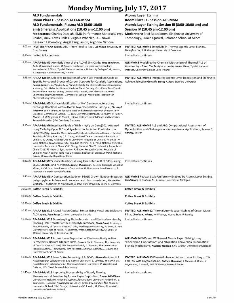
Monday Morning, July 17, 2017 13 8:00 AM
ALD Fundamentals Room Plaza F ‐ Session AF+AA‐MoM ALD Fundamentals: Plasma ALD (8:00‐10:00 am)/Emerging Applications (10:45 am‐12:00 pm) Moderators: Charles Dezelah, EMD Performance Materials, Yves Chabal, Univ. Texas Dallas, Virginia Wheeler, U.S. Naval Research Laboratory, Angel Yanguas‐Gil, Argonne National
Atomic Layer EtchingRoom Plaza D ‐ Session ALE‐MoM Atomic Layer Etching Session III (8:00‐10:00 am) and Session IV (10:45 am‐12:00 pm) Moderators: Fred Roozeboom, Eindhoven University of Technology, Sumit Agarwal, Colorado School of Mines
8:00am INVITED: AF+AA‐MoM1 ALD ‐ From Ideal to Real, Ola Nilsen, University of Oslo, Norway
INVITED: ALE‐MoM1 Selectivity in Thermal Atomic Layer Etching, Younghee Lee, S.M. George, University of Colorado
8:15am Invited talk continues. Invited talk continues.
8:30am AF+AA‐MoM3 Atomistic View of the ALD of Zinc Oxide, Timo Weckman,
Aalto University, Finland; M. Shirazi, Eindhoven University of Technology, Netherlands; S. Elliott, Tyndall National Institute, University College Cork, Ireland; K. Laasonen, Aalto University, Finland
ALE‐MoM3 Modeling the Chemical Mechanism of Thermal ALE of Alumina by HF and Tin Acetylacetonate, Simon Elliott, Tyndall National
Institute, University College Cork, Ireland
8:45am AF+AA‐MoM4 Selective Deposition of Single Site Vanadium Oxide at Specific Functional Groups of Carbon Supports for Catalytic Applications, Paxcal Düngen, N. Pfänder, Max Planck Institute for Chemical Energy Conversion; X. Huang, Fritz Haber Institute of the Max Planck Society; K.H. Böhm, Max Planck Institute for Chemical Energy Conversion; S. Buller, Max Planck Institute for Chemical Energy Conversion, Germany; R. Schlögl, Max Planck Institute for Chemical Energy Conversion
INVITED: ALE‐MoM4 Integrating Atomic Layer Deposition and Etching to Achieve Selective Growth, Stacey F. Bent, Stanford University
9:00am AF+AA‐MoM5 Surface Modification of V‐VI Semiconductors using Exchange Reactions within Atomic Layer Deposition Half‐cycle., Christoph Wiegand, Leibniz Institute for Solid State and Materials Research Dresden (IFW Dresden), Germany; R. Zierold, R. Faust, Universität Hamburg, Germany; D. Pohl, A. Thomas, B. Rellinghaus, K. Nielsch, Leibniz Institute for Solid State and Materials Research Dresden (IFW Dresden), Germany
Invited talk continues.
9:15am AF+AA‐MoM6 Interface Dipole of High k ‐Y2O3 on GaAs(001) Attained using Cycle‐by‐Cycle ALD and Synchrotron Radiation Photoelectron Spectroscopy, Wan‐Sin Chen, National Synchrotron Radiation Research Center,
Republic of China; K.‐Y. Lin, L.B. Young, National Taiwan University, Republic of China; Y.‐T. Cheng, National Chia‐Yi University, Republic of China; Y.‐H. Lin, H.‐W. Wan, National Taiwan University, Republic of China; C.‐Y. Yang, National Tsing Hua University, Republic of China; C.‐P. Cheng, National Chia‐Yi University, Republic of China; T.‐W. Pi, National Synchrotron Radiation Research Center, Republic of China; R. Kwo, National Tsing Hua University, Republic of China; M. Hong, National Taiwan University, Republic of China
INVITED: ALE‐MoM6 ALE and ALC: Computational Assessment of Opportunities and Challenges in Nanoelectronic Applications, Sumeet C.
Pandey, Micron
9:30am AF+AA‐MoM7 Surface Reactions during Three‐step ALD of SiCxNy using Si2Cl6, CH3NH2, and N2 Plasma, Rafaiel Ovanesyan, N. Leick, Colorado School of Mines; K. Kelchner, Lam Research Corporation; D. Hausmann, Lam Research; S. Agarwal, Colorado School of Mines
Invited talk continues.
9:45am AF+AA‐MoM8 A Comparative Study on PEALD Grown Nanolaminates on polypropylene: Influence of precursor and plasma variation, Maximilian
Gebhard, F. Mitschker, P. Awakowicz, A. Devi, Ruhr‐University Bochum, Germany
ALE‐MoM8 Reactor Scale Uniformity Enabled by Atomic Layer Etching, Chad Huard, S. Lanham, M. Kushner, University of Michigan
10:00am Coffee Break & Exhibits Coffee Break & Exhibits
10:15am Coffee Break & Exhibits Coffee Break & Exhibits
10:30am Coffee Break & Exhibits Coffee Break & Exhibits
10:45am AF+AA‐MoM12 A Dual Action Optical Sensor Using Metal and Dielectric ALD Layers, Sean Barry, Carleton University, Canada
INVITED: ALE‐MoM12 Thermal Atomic Layer Etching of Cobalt Metal Films, Charles H. Winter, W. Waduge, Wayne State University
11:00am AF+AA‐MoM13 Disentangling Photochromism and Electrochromism by Blocking Hole Transfer at the Electrolyte Interface, Omid Zandi, Y. Wang, J.
Kim, University of Texas at Austin; Z. Gao, Washington University, St. Louis; S. Heo, University of Texas at Austin; P. Banerjee, Washington University, St. Louis; D. Milliron, University of Texas at Austin
Invited talk continues.
11:15am AF+AA‐MoM14 Atomic Layer Deposition of Electro‐optically Active Ferroelectric Barium Titanate Films, Edward Lin, E. Ortmann, The University
of Texas at Austin; S. Abel, IBM Research‐Zurich; A. Posadas, The University of Texas at Austin; J. Fompeyrine, IBM Research‐Zurich; A. Demkov, J. Ekerdt, The University of Texas at Austin
ALE‐MoM14 WO3 and W Thermal Atomic Layer Etching Using “Conversion‐Fluorination” and “Oxidation‐Conversion‐Fluorination” Etching Mechanisms, Nicholas Johnson, S.M. George, University of Colorado
11:30am AF+AA‐MoM15 Laser Spike Annealing of ALD VO2, Alexander Kozen, U.S.
Naval Research Laboratory; R. Bell, Cornell University; B. Downey, M. Currie, U.S. Naval Research Laboratory; M. Thompson, Cornell University; V. Wheeler, C.R. Eddy, Jr., U.S. Naval Research Laboratory
INVITED: ALE‐MoM15 Plasma‐Enhanced Atomic Layer Etching of TiN and TaN with Organic Masks, Nathan Marchack, J. Papalia, R. Bruce, S.
Engelmann, E. Joseph, IBM TJ Watson Research Center
11:45am AF+AA‐MoM16 Improving Processability of Poorly Flowing Pharmaceutical Powders by Atomic Layer Deposition, Tommi Kääriäinen,
University of Helsinki, Finland; J. Nyman, Åbo Akademi University, Finland; M.‐L. Kääriäinen, P. Hoppu, NovaldMedical Ltd Oy, Finland; N. Sandler, Åbo Akademi University, Finland; S.M. George, University of Colorado; M. Ritala, M. Leskelä, University of Helsinki, Finland
Invited talk continues.
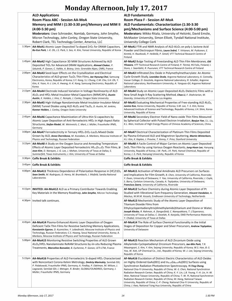
MondayAfternoon,July17,2017
Monday Afternoon, July 17, 2017 14 1:30 PM
ALD Applications Room Plaza ABC ‐ Session AA‐MoA Memory and MIM I (1:30‐3:30 pm)/Memory and MIM II (4:00‐5:30 pm) Moderators: Uwe Schroeder, Namlab, Germany, John Smythe, Micron Technology, John Conley, Oregon State University, Robert Clark, TEL Technology Center, America, LLC
ALD FundamentalsRoom Plaza F ‐ Session AF‐MoA ALD Fundamentals: Characterization (1:30‐3:30 pm)/Mechanisms and Surface Science (4:00‐5:00 pm) Moderators: Mikko Ritala, University of Helsinki, David Emslie, McMaster University, Simon Elliott, Tyndall National Institute, University College Cork
1:30pm AA‐MoA1 Atomic Layer Deposited Ta‐doped ZrO2 for DRAM Capacitors, Bo‐Eun Park, I.‐K. Oh, J.S. Park, S. Seo, H. Kim, Yonsei University, Republic of Korea
AF‐MoA1 FTIR and NMR Analysis of ALD Al2O3 on poly‐L‐lactone Acid Powder and Electrospun Fibres, Laura Svärd, T. Virtanen, M. Putkonen, E.
Kenttä, H. Rautkoski, P. Heikkilä, P. Simell, VTT Technical Research Centre of Finland
1:45pm AA‐MoA2 High Capacitance 3D MIM Structures Achieved by ALD Deposited TiO2 for Advanced DRAM Applications, Ahmad Chaker, P.
Szkutnik, P. Gonon, C. Vallée, A. Bsiesy, Univ. Grenoble Alpes, CNRS, France
AF‐MoA2 Bulge Testing of Freestanding ALD Thin Film Membranes, Oili Ylivaara, VTT Technical Research Centre of Finland; P. Törmä, HS Foils, Finland; I. Stuns, J. Saarilahti, R. Puurunen, VTT Technical Research Centre of Finland
2:00pm AA‐MoA3 Seed‐layer Effects on the Crystallization and Electrical Characteristics of ALD‐grown Ta2O5 Thin Films, Jae Hyoung Choi, Samsung
Electronics, Korea, Republic of Korea; S.Y. Kang, S.J. Chung, C.M. Cho, S.H. Oh, Y. Kim, K. Yoon, H.‐J. Lim, K. Hwang, H.‐K. Kang, Samsung Electronics, Republic of Korea
AF‐MoA3 Infiltrated Zinc Oxide in Polymethylmethacrylate: An Atomic Cycle Growth Study, Leonidas Ocola, Argonne National Laboratory; A. Connolly, Vassar College; D. Gosztola, Argonne National Laboratory; R. Schaller, Argonne National Laboratory, Northwestern University; A. Yanguas‐Gil, Argonne National Laboratory
2:15pm AA‐MoA4 Electrode Induced Variation in Voltage Nonlinearity of ALD Al2O3 and HfO2 Metal‐Insulator‐Metal Capacitors (MIMCAPs), Dustin Austin, K. Holden, J. Hinz, C. Remple, J. Conley, Oregon State University
AF‐MoA4 Study on Atomic‐Layer‐Deposited Al2O3 Dielectric Films with a New Small Angle X‐Ray Scattering Method, Chao Li, F. Shahriarian, M.
Goorsky, University of California Los Angeles
2:30pm AA‐MoA5 High‐Voltage Nanolaminate Metal‐Insulator‐Insulator‐Metal (MIIM) Tunnel Diodes using ALD Al2O3 and Ta2O5, D. Austin, M. Jenkins,
Konner Holden, J. Conley, Oregon State University
AF‐MoA5 Evaluating Mechanical Properties of Free‐standing ALD Al2O3,
Junmo Koo, Korea University, Republic of Korea; S.M. Lee, T.‐S. Kim, Korea Advanced Institute of Science and Technology, Republic of Korea; J.H. Shim, Korea University, Republic of Korea
2:45pm AA‐MoA6 Capacitance Maximization of Ultra‐thin Si‐capacitors by Atomic Layer Deposition of Anti‐ferroelectric HfO2 in High Aspect Ratio Structures, Stefan Riedel, W. Weinreich, C. Mart, J. Müller, Fraunhofer IPMS,
Germany
AF‐MoA6 Secondary Electron Yield of Nano‐oxide Thin Films Measured by Spherical Collector with Pulsed Electron Irradiation, Baojun Yan, S.L. Liu, K.L. Wen, Institute of High Energy Physics of Chinese Academy of Sciences, China
3:00pm AA‐MoA7 Ferroelectricity in Ternary HfO2‐ZrO2‐La2O3 Mixed Oxide Grown by ALD, Anna Chernikova, M. Kozodaev, A. Markeev, Moscow Institute of
Physics and Technology, Russian Federation
AF‐MoA7 Electrical Characterization of Platinum Thin Films Deposited by Plasma‐Enhanced ALD and Magnetron Sputtering, Martin Winterkorn,
H.J. Kim, K. Kaplan, J. Provine, T. Kenny, F. Prinz, Stanford University
3:15pm AA‐MoA8 A Study on the Oxygen Source and Annealing Temperature Effects of Atomic Layer Deposited Ferroelectric Hf0.5Zr0.5O2 Thin Films, Si Joon Kim, D. Narayan, J.‐G. Lee, J. Mohan, University of Texas at Dallas; S. Summerfelt, Texas Instruments; J. Kim, University of Texas at Dallas
AF‐MoA8 A Facile Control of Major Carriers on Atomic Layer Deposited SnOx Thin Film by using Various Oxygen Reactants, Jung‐Hoon Lee, Hanyang University, Republic of Korea; J.W. Park, J.R. Park, Hansol Chemical, Republic of Korea; J.‐S. Park, Hanyang University, Republic of Korea
3:30pm Coffe Break & Exhibits Coffe Break & Exhibits
3:45pm Coffe Break & Exhibits Coffe Break & Exhibits
4:00pm AA‐MoA11 Thickness Dependence of Polarization Response in (Hf,Zr)O2,
Sean Smith, M. Rodriguez, D. Henry, M. Brumbach, J. Ihlefeld, Sandia National Laboratories
AF‐MoA11 Activation of Metal Amidinate ALD Precursors on Surfaces and Implications for Film Growth, B. Chen, University of California, Riverside; Y. Duan, University of Delaware; Y. Yao, University of California, Riverside; J. Coyle, S. Barry, Carleton University, Canada; A. Teplyakov, University of Delaware; Francisco Zaera, University of California, Riverside
4:15pm INVITED: AA‐MoA12 ALD as a Primary Contributor Towards Enabling Key Materials in the Memory Roadmap, John Smythe, Micron Technology
AF‐MoA12 Surface Chemistry during Atomic‐Layer Deposition of Pt Studied with Vibrational Sum‐frequency Generation, Vincent Vandalon, A. Mackus, W.M.M. Kessels, Eindhoven University of Technology, Netherlands
4:30pm Invited talk continues. AF‐MoA13 Mechanistic Study of the Atomic Layer Deposition of Titanium Dioxide Films from Ethylcyclopentadienyltris(dimethylamido)titanium and Ozone or Water, Joseph Klesko, R. Rahman, A. Dangerfield, C. Nanayakkara, T. L’Esperance, University of Texas at Dallas; C. Dezelah, R. Kanjolia, EMD Performance Materials; Y. Chabal, University of Texas at Dallas
4:45pm AA‐MoA14 Plasma‐Enhanced Atomic Layer Deposition of Oxygen Deficient TaOx Thin Films for Resistive Switching Memory Applications, Konstantin Egorov, D. Kuzmichev, Y. Lebedinskii, Moscow Institute of Physics and Technology, Russian Federation; C.S. Hwang, Seoul National University, Korea; A. Markeev, Moscow Institute of Physics and Technology, Russian Federation
AF‐MoA14 The Role of Surface Chemical Functionality in the Initial Stages of Deposition for Copper and Silver Precursors, Andrew Teplyakov,
University of Delaware
5:00pm AA‐MoA15 Monitoring Resistive Switching Properties of ALD Grown Al2O3/HfO2 Nanolaminate ReRAM Structures by iin‐situ Reducing Plasma Treatments, Marceline Bonvalot, B. Eychenne, P. Gonon, LETI‐LTM, France
AF‐MoA15 Reaction Mechanism of ALD Zirconium Oxide using Alkylamido‐Cyclopetadienyl Zirconium Precursors, Jae‐Min Park, T.R.
Mayangsari, S. Kim, Y. Kim, Sejong University, Republic of Korea; W.S. Han, B.‐S. Yoo, W. Koh, UP Chemical Co., Ltd., Republic of Korea; W.‐J. Lee, Sejong University, Republic of Korea
5:15pm AA‐MoA16 Properties of ALD Ferroelectric Si‐doped HfO2 Characterized with Noncontact Corona‐Kelvin Metrology, Dmitriy Marinskiy, Semilab SDI;
P. Polakowski, Fraunhofer IPMS, Germany; A. Findlay, P. Edelman, M. Wilson, J. Lagowski, Semilab SDI; J. Metzger, R. Binder, GLOBALFOUNDRIES, Germany; J. Müller, Fraunhofer IPMS, Germany
AF‐MoA16 Elucidation of Distinct Electric Characteristics of ALD Oxides on Highly Ordered GaAs(001) and In0.53Ga0.47As(001) Surfaces using Synchrotron Radiation Photoelectron Spectroscopy, Yi‐Ting Cheng, National Chia‐Yi University, Republic of China; W.‐S. Chen, National Synchrotron Radiation Research Center, Republic of China; K.‐Y. Lin, L.B. Young, Y.‐H. Lin, H.‐W. Wan, National Taiwan University, Republic of China; T.‐W. Pi, National Synchrotron Radiation Research Center, Republic of China; M. Hong, National Taiwan University, Republic of China; C.‐P. Cheng, National Chia‐Yi University, Republic of China; J. Kwo, National Tsing Hua University, Republic of China
MondayAfternoon,July17,2017
Monday Afternoon, July 17, 2017 15 1:30 PM
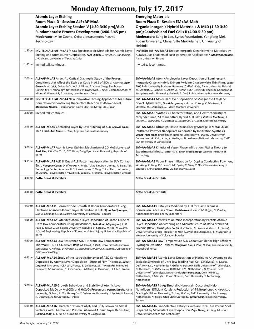
Atomic Layer Etching Room Plaza D ‐ Session ALE+AF‐MoA Atomic Layer Etching Session V (1:30‐3:30 pm)/ALD Fundamentals: Process Development (4:00‐5:45 pm) Moderator: Mike Cooke, Oxford Instruments Plasma Technology
Emerging MaterialsRoom Plaza E ‐ Session EM+AA‐MoA Organic‐Inorganic Hybrid Materials & MLD (1:30‐3:30 pm)/Catalysis and Fuel Cells II (4:00‐5:30 pm) Moderators: Sang In Lee, Synos Foundation, Yongfeng Mei, Fudan University, China, Ville Miikkulainen, University of Helsinki
1:30pm INVITED: ALE+AF‐MoA1 In situ Spectroscopic Methods for Atomic Layer Etching and Atomic Layer Deposition, Yves Chabal, J. Klesko, A. Dangerfield, J.‐F. Veyan, University of Texas at Dallas
INVITED: EM+AA‐MoA1 Unique Inorganic‐Organic Hybrid Materials by ALD/MLD as Enablers of Next‐generation Applications?, Maarit Karppinen,
Aalto University, Finland
1:45pm Invited talk continues. Invited talk continues.
2:00pm ALE+AF‐MoA3 An in situ Optical Diagnostic Study of the Process Conditions that Affect the Etch per Cycle in ALE of SiO2, S. Agarwal, Ryan
Gasvoda, N. Leick, Colorado School of Mines; A. van de Steeg, Eindhoven University of Technology, Netherlands; R. Ovanesyan, J. Klein, Colorado School of Mines; R. Bhowmick, E. Hudson, Lam Research Corp.
EM+AA‐MoA3 Atomic/molecular Layer Deposition of Luminescent Inorganic‐Organic Hybrid Erbium Pyridine Dicarboxylate Thin Films, Lukas Mai, Ruhr‐University Bochum, Germany; Z. Giedraityte, Aalto University, Finland; M. Schmidt, D. Rogalla, S. Scholz, A. Wieck, Ruhr‐University Bochum, Germany; M. Karppinen, Aalto University, Finland; A. Devi, Ruhr‐University Bochum, Germany
2:15pm INVITED: ALE+AF‐MoA4 New Innovative Etching Approaches for Future Generation by Controlling the Surface Reaction at Atomic‐Level, Masanobu Honda, T. Katsunuma, Tokyo Electron Miyagi Ltd., Japan
EM+AA‐MoA4 Molecular Layer Deposition of Manganese‐Ethylene Glycol Hybrid Films, David Bergsman, J. Baker, N. Yang, C. MacIsaac, A.
Strickler, M. Lillethorup, S.F. Bent, Stanford University
2:30pm Invited talk continues. EM+AA‐MoA5 Synthesis, Characterization, and Electrochemistry of Molybdenum‐1,2‐Ethanedithiol Hybrid ALD Films, Callisto MacIsaac, R.
Closser, J. Schneider, T. Hellstern, D. Bergsman, S.F. Bent, Stanford University
2:45pm ALE+AF‐MoA6 Controlled Layer‐by‐Layer Etching of ALD Grown Ta2O5 Thin Films, Anil Mane, J. Elam, Argonne National Laboratory
EM+AA‐MoA6 Ultrahigh Elastic Strain Energy Storage in Metal‐Oxide‐Infiltrated Polymer Nanopillars Generated by Infiltration Synthesis, Chang‐Yong Nam, Brookhaven National Laboratory; K. Dusoe, University of Connecticut; A. Stein, X. Ye, K. Kisslinger, Brookhaven National Laboratory; S.‐W. Lee, University of Connecticut
3:00pm ALE+AF‐MoA7 Atomic Layer Etching Mechanism of 2D MoS2 Layers, Ki Seok Kim, K.H. Kim, Y.J. Ji, G.Y. Yeom, Sung Kyun Kwan University, Republic of Korea
EM+AA‐MoA7 Kinetics of Vapor Phase Infiltration: Fitting Theory to Experimental Measurements, C. Leng, Mark Losego, Georgia Institute of
Technology
3:15pm ALE+AF‐MoA8 ALD & Quasi‐ALE Patterning Application in EUV Contact Etch, Hongyun Cottle, D. O’Meara, A. Metz, Tokyo Electron Limited; P. Biolsi, TEL
Technology Center, America, LLC; S. Nakamura, T. Yang, Tokyo Electron Limited; M. Honda, Tokyo Electron Miyagi Ltd., Japan; S. Morikita, Tokyo Electron Limited
EM+AA‐MoA8 Vapor Phase Infiltration for Doping Conducting Polymers, W. Wang, F. Yang, CIC nanoGUNE, Spain; C. Chen, Y. Qin, Chinese Academy of Sciences, China; Mato Knez, CIC nanoGUNE, Spain
3:30pm Coffe Break & Exhibits Coffe Break & Exhibits
3:45pm Coffe Break & Exhibits Coffe Break & Exhibits
4:00pm ALE+AF‐MoA11 Boron Nitride Growth at Room Temperature Using Electron Enhanced Atomic Layer Deposition (EE‐ALD), Jaclyn Sprenger, H. Sun, A. Cavanagh, S.M. George, University of Colorado ‐ Boulder
EM+AA‐MoA11 Catalysts Modified by ALD for Harsh Biomass Conversion Processes, Steven Christensen, K. Hurst, M. Griffin, D. Vardon,
National Renewable Energy Laboratory
4:15pm ALE+AF‐MoA12 Catalyzed Atomic Layer Deposition of Silicon Oxide at Ultra‐low Temperature using Alkylamines, Tirta Rona Mayangsari, J.‐M.
Park, L. Yusup, J. Gu, Sejong University, Republic of Korea; J.‐H. Yoo, H.‐D. Kim, JUSUNG Engineering, Republic of Korea; W.‐J. Lee, Sejong University, Republic of Korea
EM+AA‐MoA12 Effects of Alumina Incorporation by Particle Atomic Layer Deposition on Sintering and Microstructure of Yttria‐Stabilized Zirconia (8YSZ), Christopher Bartel, R. O'Toole, M. Kodas, A. Drake, A. Horrell,
University of Colorado ‐ Boulder; R. Hall, ALDNanoSolutions, Inc.; C. Musgrave, A. Weimer, University of Colorado ‐ Boulder
4:30pm ALE+AF‐MoA13 Low Resistance ALD TiN from Low Temperature Thermal N2H4 + TiCl4, Steven Wolf, M. Kavrik, J. Park, University of California
San Diego; R. Holmes, D. Alvarez, J. Spiegelman, RASIRC; A. Kummel, University of California San Diego
EM+AA‐MoA13 Low‐Temperature ALD Cobalt Sulfide for High‐Efficient Hydrogen Evolution Textiles, Donghyun Kim, J. Park, H. Kim, Yonsei University,
Republic of Korea
4:45pm ALE+AF‐MoA14 Study of the Isotropic Behavior of AZO Conductivity Deposited by Atomic Layer Deposition ‐ Effect of Film Thickness, Benoit Dugrenil, Microoled ‐ CEA Leti, France; S. Guillamet, M. Thomschke, Microoled Company; M. Tournaire, B. Aventurier, L. Mollard, T. Maindron, CEA‐Leti, France
EM+AA‐MoA14 Atomic Layer Deposition of Platinum: An Avenue to the Scalable Synthesis of Ultra‐low‐loading Fuel Cell Catalysts?, A. Goulas, Delft IMP B.V., Netherlands; F. Grillo, A. Dokania, Delft University of Technology, Netherlands; D. Valdesueiro, Delft IMP B.V., Netherlands; H. Van Bui, Delft University of Technology, Netherlands; Bart van Limpt, Delft IMP B.V., Netherlands; J. Moulijn, J.R. van Ommen, Delft University of Technology, Netherlands
5:00pm ALE+AF‐MoA15 Growth Behaviour and Stability of Atomic Layer Deposited MoO3 by Mo(CO)6 and H2O/O3 Precursors, Perttu Sippola, Aalto University, Finland; Z. Zhu, Beneq Oy; T. Sajavaara, University of Jyväskylä, Finland; H. Lipsanen, Aalto University, Finland
EM+AA‐MoA15 Pd‐Ag Bimetallic Nanograin‐Decorated Nylon Nanofibers: Efficient Catalytic Reduction of 4‐Nitrophenol, K. Ranjith, A. Celebioglu, Bilkent University, Turkey; H. Eren, Delft University of Technology, Netherlands; N. Biyikli, Utah State University; Tamer Uyar, Bilkent University, Turkey
5:15pm ALE+AF‐MoA16 Characterization of Al2O3 and HfO2 Grown on Metal Surfaces with Thermal and Plasma Enhanced Atomic Layer Deposition, Haiping Zhou, Y.‐C. Fu, M. Mirza, University of Glasgow, UK
EM+AA‐MoA16 Size‐Selective Catalysts with an Ultra‐Thin Porous Shell Prepared by Molecular Layer Deposition, Zeyu Shang, X. Liang, Missouri
University of Science and Technology
MondayEveningPosterSessions,July17,2017
Monday Evening Poster Sessions, July 17, 2017 16 5:30 PM
ALD Fundamentals Room Plaza Exhibit ‐ Session AF‐MoP ALD Fundamentals Poster Session 5:30pm
AF‐MoP1 Template‐Free Vapor‐Phase Growth of Patrónite (VS4) by Atomic Layer Deposition, Matthew Weimer, R. McCarthy, Argonne National Laboratory; J.
Emery, M. Bedzyk, Northwestern University; F. Sen, A. Kinaci, M. Chan, A. Hock, A. Martinson, Argonne National Laboratory
AF‐MoP2 Novel Approach to Deposit Carbon Doped Silicon Oxide Film with High Carbon Content via Thermal ALD, Haripin Chandra, K. Cuthill, Versum
Materials, Inc; M. MacDonald, G. Sanchez, Versum Materials, Inc.; A. Mallikarjunan, Versum Materials, Inc
AF‐MoP3 A New Reducing Co‐Reagent and Challenges in Thermal Atomic Layer Deposition of Electropositive Metal Films, Kyle Blakeney, C.H. Winter,
Wayne State University
AF‐MoP4 Volatile Rare Earth Metal Alkoxides for ALD precursors, Atsushi Sakurai, ADEKA Corporation, Japan; N. Sugiura, M. Hatase, A. Nishida, A. Yamashita, ADEKA Corporation
AF‐MoP5 Enabling Smooth and Conformal Film Growth via Separate Surface Treatment during Atomic Layer Deposition of Cobalt, Jeong‐Seok Na, Lam
Research Corp.
AF‐MoP6 Comparative Study of ALD SiO2 Films, Andy Zauner, Air Liquide R&D, France; J.‐M. Girard, Air Liqude Advanced Materials, France
AF‐MoP7 B2O3 ALD for Advanced Doping Applications: The Roles of Free Radical Precursors and Surface Composition, A. Pilli, J. Jones, Jeffry Kelber, University of North Texas; F. Pasquale, A. LaVoie, Lam Research Corp.
AF‐MoP8 High‐aspect Ratio Anodic TiO2 Nanotube Layers: Unprecedented Ability of ALD to add a Functionality, Raul Zazpe, J. Přikryl, H. Sopha, L. Hromadko,
J. Macák, University of Pardubice, Czech Republic
AF‐MoP9 PEALD Ga2O3 as Dielectric Interlayer on GaN, Mei Hao, R. Nemanich,
S. Chowdhury, Arizona State University
AF‐MoP10 Effect of Deposition Temperature and Plasma Condition on Film Quality of TiO2 Deposited by Plasma‐Enhanced Atomic Layer Deposition, Munehito Kagaya, Tokyo Electron Limited, Japan; S. Iwashita, Tokyo Electron Yamanashi Limited, Japan; Y. Suzuki, Y. Sakamoto, Tokyo Electron Limited, Japan; A. Uedono, University of Tsukuba, Japan; T. Mitsunari, Tokyo Electron Limited, Japan; N. Shindo, M. Yamasaka, N. Noro, T. Hasegawa, Tokyo Electron Yamanashi Limited, Japan; T. Moriya, Tokyo Electron Limited, Japan
AF‐MoP11 Atom Probe Tomography of Platinum and Ruthenium Atomic Layer Deposition Films, Daniel Potrepka, B. Hornbuckle, U.S. Army Research
Laboratory; N. Strnad, University of Maryland
AF‐MoP12 Nitrogen Doped Al2O3 Films with High Doping Uniformity and Low Film Roughness Grown by Plasma Enhanced Atomic Layer Deposition, Hong‐Yan Chen, H.‐L. Lu, Fudan University, China
AF‐MoP13 Study on the Gate Sidewall Spacer Silicon‐Nitride ALD Process at Low Temperature by High Density Multiple ICP Sources, Ho‐Hyun Song, H.‐Y. Chang, Y. Seol, KAIST, Republic of Korea
AF‐MoP14 Effect of Revolution and Rotating Substrate for ALD SiO2 Film at Low Temperature Using SDP System, Jin‐Hyuk Yoo, B.H. Cho, JUSUNG
Engineering, Republic of Korea
AF‐MoP15 Breakthrough Trace Element Analysis for Challenging ALD Film Precursors, Lisa Mey‐Ami, J. Wang, H. Gotts, F. Li, Air Liquide ‐ Balazs NanoAnalysis
AF‐MoP16 New Technology Advances of Electromechanical Valve Technology for Precision‐Controlled Millisecond Pulsed Delivery in ALD/ALE Applications, Patrick Lowery, HORIBA; H. Nishizato, Horiba Stec, Japan; J. Dick, T.
Hoke, HORIBA
AF‐MoP17 Band Alignment at the Interface of Atomic Layer Deposition Al2O3
and Ga‐Polar GaN under Ultraviolet/Ozone Treatment, K. Kim, J.H. Ryu, J. Kim,
S.J. Cho, D. Liu, J. Park, I. Lee, University of Wisconsin‐Madison; B. Moody, HexaTech. Inc.; W. Zhou, University of Texas at Arlington; J. Albrecht, Michigan State University; Zhenqiang Ma, University of Wisconsin‐Madison
AF‐MoP18 Raman Spectrum Characterization of Ti‐based ALD Thin Films Treated with Ultra‐high Vacuum Annealing, Chengchun Tang, X.S. Jia, C.Z. Gu, J.J. Li, Institute of Physics, Chinese Academy of Sciences, China
AF‐MoP20 Complete Analytical Characterization of Surface, Interfacial and Bulk Layers of ALD Films: The Path to Improved and Reliable Deposition Processes, Yagnaseni Ghosh, C. Langland, W. Rivello, F. Li, Air Liquide ‐ Balazs
NanoAnalysis
AF‐MoP21 Sequential Exposures of N2H4 + BCl3 on Copper, HOPG and Si0.7Ge0.3 Surfaces, Steven Wolf, M. Breeden, M. Edmonds, K. Sardashti, M. Clemons,
University of California San Diego; E. Yieh, H. Ren, S. Nemani, Applied Materials; D. Alvarez, RASIRC; A. Kummel, University of California San Diego
AF‐MoP22 Plasma Enhanced ALD of BN, B‐doped SiN and B‐doped TiN, Moo‐
Sung Kim, Versum Materials Korea, Republic of Korea; X. Lei, Versum Materials, Inc; S.‐H. Yang, Versum Materials Korea, Republic of Korea
AF‐MoP23 Scale‐Up of Atomic Layer Deposition on Powders in Fixed Bed Reactors, Kristian Knemeyer, V.E. Strempel, P. Ingale, R. Naumann d'Alnoncourt,
BasCat, UniCat BASF JointLab, Technische Universität Berlin, Germany; A. Thomas, M. Driess, Institut für Chemie, Technische Universität Berlin, Germany; F. Rosowski, BASF SE, Germany
AF‐MoP24 Measurement and Control of Stress of ALD Films and Nano‐laminates Measured by Interferometry, Ritwik Bhatia, Ultratech
AF‐MoP25 Temperature Dependent Kinetics of ALD Reaction: SiN PEALD Study, Triratna Muneshwar, C. Cadien, University of Alberta, Canada
AF‐MoP26 Process Development and Characterization of the Atomic Layer Deposited MoS2, Tian‐Bao Zhang, J. Xu, Y. Wang, L. Chen, Q.‐Q. Sun, H. Zhu, S.‐J.
Ding, D.W. Zhang, Fudan University, China
AF‐MoP27 Low Energy Ion Scattering (LEIS) Analysis of ALD Deposited GaSb Films on SiO2, Philipp Brüner, ION‐TOF GmbH, Germany; T. Grehl, ION‐TOF GmbH; R.
ter Veen, Tascon GmbH, Germany; M. Fartmann, Tascon GmbH; T. Blomberg, M. Tuominen, ASM, Finland
AF‐MoP28 Alternative Plasma Gas Chemistries for Plasma Enhanced Atomic Layer Deposition and the 2016 PEALD Publication Review, Plasma‐ALD Guy,
www.plasma‐ald.com
AF‐MoP29 Characterization of Ultra‐thin ALD Coating in Mesoporous Silicon Layers, Andras Kovacs, U. Mescheder, Furtwangen University, Germany
AF‐MoP30 Hydrogen Impurities in Al2O3 Thin Films using TMA and Heavy Water as Precursors, Sami Kinnunen, K. Arstila, M. Lahtinen, T. Sajavaara, University
of Jyväskylä, Finland
AF‐MoP31 Density Functional Theory Calculation on the Reaction Between Different Nitriding Agents and Chlorine‐terminated Silicon Nitride Surface, Luchana Yusup, T.R. Mayangsari, J.‐M. Park, Sejong University, Republic of Korea; Y.‐K. Kwon, Kyung Hee University, Republic of Korea; W.‐J. Lee, Sejong University, Republic of Korea
AF‐MoP32 Edge‐On MoS2 Thin Films by Direct Atomic Layer Deposition for Hydrogen Evolution Reaction, Changdeuck Bae, T.A. Ho, H. Shin, Sungkyunkwan University
AF‐MoP33 Role of Initial Precursor Chemisorption on Incubation Delay for Molybdenum Oxide Atomic Layer Deposition, Charith Nanayakkara, EMD
Performance Materials; A. Vega, University of Texas at Dallas; G. Liu, C. Dezelah, R. Kanjolia, EMD Performance Materials; Y. Chabal, University of Texas at Dallas
AF‐MoP34 Precursor Screening for Low Temperature Atomic Layer Deposition of SiO2 using Ozone, Dingkai Guo, B. Hendrix, T. Baum, Entegris Inc.
AF‐MoP35 Surface Treatments on Vertically Aligned Carbon Nanotube Forests for Atomic Layer Deposition, David Kane, R. Vanfleet, R. Davis, Brigham
Young University
AF‐MoP36 Quantum Chemical Design for Kinetically Enhanced ALD Precursors, Thomas Mustard, Schrodinger, Inc.; C.H. Winter, Wayne State University,
USA; M. Halls, Schrodinger, Inc.
AF‐MoP37 QDB: A Database of Plasma Process Data, C. Hill, S. Rahimi, D.
Brown, Anna Dzarasova, Quantemol Ltd, UK; J. Hamilton, K. Wren‐Little, University College London, UK; S. Mohr, Quantemol Ltd, UK; J. Tennyson, University College London, UK
AF‐MoP38 Surface Functionalization of Few‐layer MoS2 for Atomic Layer Deposition using Gold Chloride Salts, Jaron Kropp, T. Gougousi, University of Maryland, Baltimore County
AF‐MoP39 Atomic layer deposition of ZrO2 thin film using a novel linked cyclopentadienyl‐amido Zr precursor, Mira Park, J.H. Kwon, Y. Lee, J.R. Park, S.
Kim, H. Ahn, S. Yun, J.W. Park, Hansol Chemical, Republic of Korea
MondayEveningPosterSessions,July17,2017
Monday Evening Poster Sessions, July 17, 2017 17 5:30 PM
AF‐MoP40 Surface Oxidation of Titanium Oxynitride Films Prepared by PEALD, J. Łobaza, M. Kot, Brandenburg University of Technology Cottbus‐Senftenberg,
Germany; F. Naumann, Hassan Gargouri, Sentech Instruments, Germany; K. Henkel, D. Schmeißer, Brandenburg University of Technology Cottbus‐Senftenberg, Germany
AF‐MoP41 Characterization of SiNx Plasma Enhanced Atomic Layer Deposition Process, Sun Jung Kim, S.H. Yong, H. Chae, Sungkyunkwan University
(SKKU), Republic of Korea
AF‐MoP42 Transient Response of ALD‐QCM with Synchronized Back Pressure Control of Sensor Head, S. Tanaka, Tohoku University, Japan; K. Hikichi, Techofine Co., Japan; Masafumi Kumano, Tohoku University, Japan
AF‐MoP43 Precise Thickness Controllable Al2O3 Thin Film Using Non‐Pyrophoric Al Precursors and Atomic Layer Deposition, Donghak Jang, S.J. Yeo, K.‐Y. Mun, Hansol Chemical; J.W. Park, Hansol Chemical, Republic of Korea
AF‐MoP44 Diagnostic ALD Reactor with Multiple Modes of FT‐IR Spectroscopy, B. Sperling, James Maslar, B. Kalanyan, National Institute of Standards
and Technology
AF‐MoP45 Leveraging Atomistic Modeling for Insights into Nucleation of Cobalt Precursors on Various Substrates, Andrew Adamczyk, A. Cooper, Versum
Materials; M.‐S. Kim, Versum Materials Korea, Republic of Korea; S. Ivanov, Versum Materials
AF‐MoP46 Crystalline AlN Films on Si(100) with Sharp Interface and Good Uniformity at Low Temperature by Plasma Enhanced ALD, Xinhe Zheng, S. Liu, Y. He, M. Li, J. Wang, C. Hou, University of Science and Technology Beijing, China
AF‐MoP47 Comparison between PEALD‐TiN Films using TiCl4 or TDMAT as Ti‐precursor, Hans‐Dieter Schnabel, Westsächsische Hochschule Zwickau, Germany;
T. Junghans, U. Reinhold, C. Reinhold, Westsächsische Hochschule Zwickau
AF‐MoP48 High‐speed Spectroscopic Ellipsometry for ALD Applications, Gai Chin, ULVAC Inc., Japan
AF‐MoP49 UHV FT‐IR Spectroscopy for Atomic Layer Deposition: An Instrumental Contribution, X. Stammer, Bruker Optics, Ettlingen, Germany; Richard
Merk, S. Shilov, Bruker Optics
AF‐MoP50 New Tungsten Precursors at Scale ‐ Properties and ALD Application, Andreas Wilk, A. Rivas Nass, R. Ramon‐Müller, O. Briel, Umicore AG &
Co. KG, Germany
AF‐MoP51 The Effect of Precursor Ligands and Substitution Chemistry on the Nucleation and Structure of Layered Chalcogenides, H. Zhang, Adam Hock, Illinois Institute of Technology
ALD for Manufacturing Room Plaza Exhibit ‐ Session AM‐MoP ALD for Manufacturing Poster Session 5:30pm
AM‐MoP1 Anhydrous Hydrogen Peroxide Gas Delivery for Semiconductor Manufacturing: Optimal Delivery Conditions for ALD Processes, D. Alvarez, J. Spiegelman, Keisuke Andachi, R. Holmes, Z. Shamsi, RASIRC
AM‐MoP2 OpenALD ‐ A Framework for an Open Source ALD Reactor, Vivek Dwivedi, NASA
AM‐MoP3 Multilayer ALD Metal Oxide Films Deposited by Spatially Resolved ALD Processes for Moisture Barrier Films, Sang Heon Yong, S.J. Kim, H. Chae,
Sungkyunkwan University (SKKU), Republic of Korea
AM‐MoP4 A Green Precleaning Process in Wettability Improvement for Thinner and Uniform ALD Al2O3 Film Deposition on Layered MoS2 Film,
Cheng‐Ying Wang, National Taiwan Normal University, Taiwan; Y.‐T. Ho, Y.‐C. Chu, National Chiao Tung University, Republic of China; H.‐R. Hsu, ITRI, Republic of China; B.‐M. Chen, P.‐S. Chen, Minghsin University of Science & Technology, Taiwan; M.‐H. Lee, National Taiwan Normal University, Taiwan; C.‐A. Jong, NARLabs, Republic of China
AM‐MoP5 Highly Sensitive Ion Trap Mass Spectrometer for Inline Process Control, Ruediger Reuter, V. Derpmann, G. Fedosenko, A. Laue, T. Graber, M. Aliman,
H.Y. Chung, Carl Zeiss SMT GmbH, Germany
AM‐MoP6 STD‐PEALD Equipment Design and Evaluation of Nano Thin‐Film Characteristics, M.H. Jeong, Korea Electronics Technology Institute, Republic of
Korea; T.Y. Ryu, Sung Kyun Kwan University; K.‐P. Hong, Korea Electronics Technology Institute, Republic of Korea; J. Choi, Sung Kyun Kwan University; C.K. Song, M. Koo, LEED Corp.; Yekyung Kim, S.H. Chang, Korea Electronics Technology Institute, Republic of Korea; I. Jeong, LEED Corp.; H. Kim, Korea Electronics Technology Institute, Republic of Korea
AM‐MoP7 Demonstration of a Correlation between Barrier Property and Defect Visualization of ALD(Al2O3)/Graphene Film, K.‐P. Hong, M.H. Jeong, D.
Lee, J.W. Seo, S.J. Lee, Korea Electronics Technology Institute, Republic of Korea; J. Choi, Sung Kyun Kwan University; I. Jeong, LEED Corp.; S.H. Chang, Yekyung Kim, H. Kim, Korea Electronics Technology Institute, Republic of Korea
AM‐MoP8 Transport and Kinetics of a Remote DBD Plasma for ALD Processing of Metal Oxides, T. Beekman, Yves Creyghton, J. Emmelkamp,
Solliance/TNO, Netherlands; A. Sobota, Eindhoven University of Technology, Netherlands
AM‐MoP9 Effects of Sealing Components on ALD Film Quality, Fred Pourmirzaie, Flodynamix
Area Selective ALD Room Plaza Exhibit ‐ Session AS‐MoP Area Selective ALD Poster Session 5:30pm
AS‐MoP1 Area‐selective ALD using Vapor and Solution‐Phase Synthesized Perfluorodecyltrichlorosilane (FDTS) SAMs as Growth Inhibition Layers, Ali Haider, Bilkent University, Turkey; S. Altuntas, TOBB University of Economics & Technology, Turkey; P. Deminskyi, T. Khan, Bilkent University, Turkey; F. Buyukserin, TOBB University of Economics & Technology, Turkey; N. Biyikli, Utah State University
AS‐MoP2 Nanoscale Patterning of C4F8 Plasma Polymer Blocking Layers via Femtosecond Pulsed Laser Processing for Selective Deposition of Noble Metals, Petro Deminskyi, I. Pavlov, S. Ilday, O. Tokel, Bilkent University, Turkey; H.
Eren, Delft University of Technology, Netherlands; A. Haider, F. Ilday, Bilkent University, Turkey; N. Biyikli, Utah State University
AS‐MoP3 Feasibility Study of Single and Multi‐layered Graphene as Plasma‐compatible Deactivation Layers for Selective Deposition of III‐Nitride Materials, Petro Deminskyi, E. Kovalska, A. Haider, C. Kocabas, Bilkent University,
Turkey; N. Biyikli, Utah State University
AS‐MoP4 Electroless Noble Metal Deposition ‐ A New Approach for Highly Selective Surface Controlled Deposition Process, Stanko Brankovic, Universtiy of Houston; D. Solanki, D. Wu, University of Houston; Y. Dordi, A. Joi, Lam Research
AS‐MoP5 Inherently Selective Plasma‐assisted ALD: A Feasibility Study for III‐Nitride Materials, Necmi Biyikli, Utah State University; A. Haider, P. Deminskyi,
Bilkent University, Turkey
Emerging Materials Room Plaza Exhibit ‐ Session EM‐MoP Emerging Materials Poster Session 5:30pm
EM‐MoP1 ALD of Copper(I) Halide Direct Bandgap Semiconductors, T. Homola, R. Krumpolec, David Cameron, Masaryk University, Czech Republic; R. Zazpe, J. Přikryl, J. Macák, University of Pardubice, Czech Republic; P. Maydannik, Lappeenranta University of Technology, Finland; G. Natarajan, Indira Gandhi Centre for Atomic Research, India
EM‐MoP2 Atomic Layer Deposition of Topological Insulator Selenides and Tellurides, Tommi Tynell, C. Wiegand, A. Thomas, K. Nielsch, Leibniz Institute for Solid
State and Materials Research Dresden (IFW Dresden), Germany
EM‐MoP3 New precursor for low temperature deposition of SiO2 layer using thermal and plasma enhanced ALD techniques, Hima Lingam, V. Chitturi, P.
Cobb, Nova‐Kem; M. Boleslawski, D. Suh, C. Choi, H. Jeong, Wonik Materials
EM‐MoP4 Modeling of the Reactions of Hexachlorodisilane on NH and NH2 Functionalized Silicon Nitride Surface, X. Wang, The Dow Chemcal Company;
Xiaobing Zhou, B. Hwang, The Dow Chemical Company; B. Ketola, B. Rekken, T. Sunderland, A. Millward, M. Telgenhoff, V. Shamamian, C. Lee, Y. Ahn, W. Chung, The Dow Chemcal Company
EM‐MoP5 New Silicon precursor for Low Temperature SiNx ALD Applications, H. Lingam, Venkateswara Chitturi, Nova‐Kem; M. Boleslawski, C. Choi,
H. Jeong, D. Suh, Wonik Materials
EM‐MoP6 Structure and Growth Behavior of MLD Films Using Cyclic Azasilanes, Maleic Anhydride, Trimethylaluminum and Water, Ling Ju, N. Strandwitz, Lehigh University
EM‐MoP7 Divalent Group IV Precursors for Atomic Layer Deposition Features, M.H. Nim, Hyunkee Kim, K.‐Y. Mun, J.R. Park, J.W. Park, Hansol Chemical,
Republic of Korea
MondayEveningPosterSessions,July17,2017
Monday Evening Poster Sessions, July 17, 2017 18 5:30 PM
EM‐MoP8 Plasma Enhanced Atomic Layer Deposition of Aluminium Sulphide, J. Kuhs, Z. Hens, Christophe Detavernier, Ghent University, Belgium
EM‐MoP9 The Film Property of Super‐cycled Al2O3/SnOx Atomic Layer Deposition and the Associated Thin Film Transistor Performance, Seung‐Hwan
Lee, S.‐J. Choi, Hanyang University, Korea; J.‐S. Park, Hanyang University, Republic of Korea
EM‐MoP10 Optical Properties and XPS Analyses of TixSi(1‐x)O2 Films Prepared by ALD and Comparison to ab‐initio Predictions, Marek Elias, CEITEC, Brno
University of Technology, Czech Republic; P. Ondracka, Masaryk University, Czech Republic; D. Necas, CEITEC, Masaryk University, Czech Republic; J. Vida, Masaryk University, Czech Republic; E. Kedronova, L. Zajickova, CEITEC, Masaryk University, Czech Republic
EM‐MoP11 Atomic Layer Deposition of MoOx:N films: Electrical and Electrochemical Properties, Arpan Dhara, D. Saha, S. Sarkar, Indian Institute of Technology Bombay, India
EM‐MoP12 In Situ Characterization of Thin Film Molybdenum Carbide using Spectroscopic Ellipsometry, Adam Bertuch, Ultratech; J. Hoglund, SemiLab; L.
Makai, Semilab; J. Byrnes, SemiLab; J. McBee, G. Sundaram, Ultratech
EM‐MoP13 Molecular Layer Deposition of Boron Carbide from Carboranes, Michelle Paquette, L. Dorsett, S. Malik, A. Caruso, University of Missouri‐Kansas City; J. Bielefeld, S. King, Intel Corporation
EM‐MoP14 Sub‐10 nm Scalable Hybrid Dielectric Engineering on MoS2 for 2D Materials Based Devices, Lanxia Cheng, J. Lee, H. Zhu, A.V. Ravichandran, Q. Wang, A. Lucero, M. Kim, R. Wallace, University of Texas at Dallas; L. Colombo, Texas Instruments, USA; J. Kim, University of Texas at Dallas
EM‐MoP15 Critical Layer Thickness Determination for GaN Thin Films Grown on Sapphire Substrate via Hollow‐Cathode Plasma‐assisted Atomic Layer Deposition, Mustafa Alevli, N. Gungor, Marmara University; N. Biyikli, Utah State
University
EM‐MoP16 Digital Doping of ALD VO2 for Thermochromic Applications, Alexander Kozen, M. Currie, U.S. Naval Research Laboratory; K. Jungjohann, Sandia National Laboratory; B. Downey, C.R. Eddy, Jr., V. Wheeler, U.S. Naval Research Laboratory
EM‐MoP17 Characterization and Comparison of ALD Laminate Structures with HfO2 + SiO2 as MIM Capacitor Dielectric for GaAs HBT Device, Yao‐Ting Shao, C.‐H. Hua, WIN Semiconductors Corp., Republic of China
EM‐MoP18 Atomic Layer Deposition of Mo‐doped VO2 Thin Films by Nanolamination of VO2/MoO3 Alternating Layers, Xinrui Lv, Y. Yu, Y. Cao, Chinese Academy of Sciences, China
EM‐MoP19 Trace Metal Analysis on SiC Wafers using ICP‐MS, Jaya
Chowdhury, ChemTrace
EM‐MoP23 Atomic Layer Deposited Single Crystal High‐k Y‐doped Cubic HfO2 on GaAs(001) Utilizing HfO2/Y2O3 Super‐cycles, Lawrence Boyu Young, C.‐
K. Cheng, Y.‐H. Lin, K.‐Y. Lin, National Taiwan University, Republic of China; C.‐H. Hsu, National Synchrotron Radiation Research Center, Republic of China; J. Kwo, National Tsing Hua University, Republic of China; M. Hong, National Taiwan University, Republic of China
Room Plaza Exhibit ‐ Session ALE‐MoP Atomic Layer Etching Poster Session 6:00pm
ALE‐SaP1 Quasi‐Atomic Layer Etching of Silicon Nitride with Tunable Directionality and Ultra‐high Selectivity, Sonam Sherpa, A. Ranjan, Tokyo Electron
ALE‐SaP2 Atomic Layer Etching with Gas Cluster Ion Beam Irradiation in Reactive Gas Vapor, Noriaki Toyoda, University of Hyogo, Japan; A. Ogawa, University of Hyogo; I. Yamada, Univeristy of Hyogo
ALE‐SaP3 Thermal Atomic Layer Etching of TiO2 using Sequential Exposures of WF6 and BCl3, P. Lemaire, Gregory N. Parsons, North Carolina State University
ALE‐SaP4 Etch Profile Control of ALD‐SiO2 Film Assisted by Alternating ALE Process of Fluorocarbon Deposition and O2 Plasma Etching, Masaru Zaitsu,
ASM, Japan; T. Tsutsumi, Nagoya University, Japan; A. Kobayashi, ASM; H. Kondo, M. Hori, Nagoya University, Japan; T. Nozawa, N. Kobayashi, ASM
ALE‐SaP5 In Situ Mass Spectrometer Studies of Volatile Etch Products During Thermal Al2O3 Atomic Layer Etching Using HF and Trimethylaluminum, Joel
Clancey, S.M. George, University of Colorado ‐ Boulder
ALE‐SaP6 Cyclic Plasma Cleaning Process of SiO2 Layers using Surface Fluorination, Kyongbeom Koh, H. Chae, Sungkyunkwan University (SKKU), Republic of
Korea
ALE‐SaP7 Low Damage Cyclical Etching of GaN and AlGaN, A. Goodyear, Oxford Instruments Plasma Technology, UK; P. Abrami, University of Bristol, UK; Mike Cooke, M. Loveday, Oxford Instruments Plasma Technology
ALE‐SaP8 Thermal Atomic Layer Etching of ZnO by “Conversion‐Etch” Using Hydrogen Fluoride and Trimethylaluminum, David Zywotko, S.M. George,
University of Colorado ‐ Boulder
ALE‐SaP9 Cryogenic Atomic Layer Etching of SiO2, N. Holtzer, Thomas Tillocher,
P. Lefaucheux, R. Dussart, GREMI Université d'Orléans/CNRS, France
ALE‐SaP10 SF4 as a New Fluorine Reagent for Thermal ALE: Application to Al2O3 and VO2 ALE, Jonas Gertsch, N. Johnson, V. Bright, S.M. George, University of
Colorado ‐ Boulder
ALE‐SaP11 Demonstrating Manufacturability of Atomic Level Etch (ALE) through Accelerated Neutral Atom Beam (ANAB) Processing, Daniel Steinke, B. Sapp, S. PapaRao, SUNY Polytechnic Institute; E. Barth, SEMATECH; V. Kaushik, M. Rodgers, C. Hobbs, SUNY Polytechnic Institute; M. Walsh, S. Kirkpatrick, R. Svrluga, Neutral Physics Corporation
ALE‐SaP12 Etching with Low Te Plasmas, Scott Walton, D. Boris, U.S. Naval
Research Laboratory; S. Hernández, U.S.Naval Research Laboratory; H. Miyazoe, A. Jagtiani, S. Engelmann, E. Joseph, IBM TJ Watson Research Center
ALE‐SaP13 Surface Cleaning of Gallium Antimonide Oxides: The Role of Hydrogen Atoms, Argon Ions, and Temperature, Thomas Larrabee, S. Prokes,
Naval Research Laboratory
ALE‐SaP14 Aluminum Native Oxide Surface Cleaning and Passivation in an Atmospheric Plasma System, John Mudrick, M. Pohl, K. Knisely, Sandia National
Laboratories
ALE‐SaP15 Atomic Layer Etching in Reactive Ion Etching System for Nanoscale Pattern Transfer, S. Khan, Dmitry Suyatin, M. Graczyk, A. Kvennefors,
Lund University, Sweden; E. Kauppinen, Aalto University, Finland; M. Huffman, I. Maximov, Lund University, Sweden; J. Sundqvist, Fraunhofer Institute for Ceramic Technologies and Systems IKTS, Germany
ALE‐SaP16 Selective Fluorocarbon‐based Atomic Layer Etching in a Conventional Parallel‐Plate, Capacitively Coupled Plasma, Stefano Dallorto, Ilmenau University of Technology; A. Goodyear, Oxford Instruments Plasma Technology, UK; M. Cooke, Oxford Instruments Plasma Technology; S. Dhuey, A. Schwartzberg, S. Sassolini, Lawrence Berkeley National Laboratory; C. Ward, Oxford Instruments; D. Olynick, Lawrence Berkeley National Laboratory; I. Rangelow, Ilmenau University of Technology; S. Cabrini, Lawrence Berkeley National Laboratory
ALE‐SaP17 RF Plasma Electrostatics: The Influence on Film Morphology and Carbon Incorporation, K. Scott Butcher, Meaglow Ltd, Canada; P. Terziyska, Institute
of Solid State Physics, Bulgarian Academy of Sciences, Bulgaria; V. Georgiev, Meaglow Ltd, Canada; D. Georgieva, Semiconductor Research Lab, Lakehead University, Canada; R,. Gergova, Central Laboratory of Solar Energy and New Energy Sources, Bulgarian Academy of Sciences, Bulgaria; P. Binsted, S. Skergetc, Semiconductor Research Lab, Lakehead University, Canada
ALE‐SaP18 Atomic Layer Etching of Amorphous Silicon with Selectivity Towards MoS2, Markus Heyne, KU Leuven, Belgium; A. Goodyear, Oxford
Instruments Plasma Technology, UK; J.‐F. de Marneffe, IMEC, Belgium; M. Cooke, Oxford Instruments Plasma Technology, UK; I. Radu, IMEC, Belgium; E. Neyts, University of Antwerp, Belgium; S. De Gendt, KU Leuven, Belgium
ALE‐SaP19 Simulation of New Material‐Systems for Directional Atomic Layer Etching, Ivan Berry, K.J. Kanarik, T. Lill, V. Vahedi, R. Gottscho, Lam Research Corp.
TuesdayMorning,July18,2017
Tuesday Morning, July 18, 2017 19 8:00 AM
ALD Applications Room Plaza F ‐ Session AA+AF‐TuM Displays and Flexible Applications (8:00‐10:00 am)/ALD Fundamentals: In‐Situ Monitoring and Analysis (10:45 am‐12:00 pm) Moderators: Hyungjun Kim, Yonsei University, Jin‐Seong Park, Hanyang University, Han‐Jin Lim, Samsung Electronics, Tom Knisley, Applied Materials
ALD ApplicationsRoom Plaza ABC ‐ Session AA‐TuM Batteries I (8:00‐10:00 am)/Emerging Apps II (10:45 am‐12:00 pm) Moderators: Christophe Detavernier, Ghent University, Christophe Vallee, LETI‐LTM, France, Tero Pilvi, Picosun Oy
8:00am INVITED: AA+AF‐TuM1 Functional Materials using Atomic Layer Deposition for Emerging Display Applications, Jin‐Seong Park, Hanyang University, Republic of Korea
INVITED: AA‐TuM1 Designing of Surface and Interface of Electrodes for Highly‐stable Li Ion Batteries, Li‐S Batteries and Metal‐Air Batteries, Xueliang Sun, University of Western Ontario, Canada
8:15am Invited talk continues. Invited talk continues.
8:30am AA+AF‐TuM3 Flexible Platinum Nanoparticle‐based Piezoresistive Transducers Elaborated by Atomic Layer Deposition, Etienne Puyoo, C. Malhaire, D. Thomas, R. Rafaël, Institut des Nanotechnologies de Lyon, France; M. R'Mili, A. Malchère, L. Roiban, S. Koneti, M. Bugnet, MATEIS, France; A. Sabac, M. Le Berre, Institut des Nanotechnologies de Lyon, France
AA‐TuM3 ALD Vanadium Oxides for 3D Thin‐film Lithium Ion Batteries, Felix Mattelaer, Ghent University, Belgium; K. Geryl, T. Dobbelaere, G. Rampelberg, J. Dendooven, Ghent University; C. Detavernier, Ghent University, Belgium
8:45am AA+AF‐TuM4 Color Coating of Electronic Textiles via Control of Refractive Index by Atomic Layer Deposition, Hyun Gu Kim, W.H. Kwon,
H.B.R. Lee, Incheon National University, Republic of Korea
AA‐TuM4 PE‐ALD of Transition Metal Phosphates as Lithium‐Ion Battery Electrode Materials, T. Dobbelaere, F. Mattelaer, J. Dendooven, Ghent
University, Belgium; P. Vereecken, Imec, Belgium; Christophe Detavernier, Ghent University, Belgium
9:00am AA+AF‐TuM5 Comprehensive Studies of Atomic Layer Deposited InGaO Thin Films using InCA‐1, TMGa and H2O2 for Oxide Semiconductor Thin Film Transistor Applications, Jiazhen Sheng, Hanyang University, Republic of Korea; B. Shong, Chungnam National University, Republic of Korea; J.‐S. Park, Hanyang University, Republic of Korea
AA‐TuM5 Comparing Temporal and Spatial Atomic Layer Deposition for Enhanced Performance of Li Ion Battery Electrodes, Alexander Yersak, A. Dameron, University of Colorado ‐ Boulder; X. Li, Y. Yang, Colorado School of Mines; K. Hurst, R. Tenet, National Renewable Energy Laboratory; S.M. George, University of Colorado – Boulder
9:15am AA‐TuM6 All‐Solid‐State Thin‐Film Battery with a Novel Organic Cathode Material by Atomic/Molecular Layer Deposition, Mikko Nisula, M.
Karppinen, Aalto University, Finland
9:30am AA+AF‐TuM7 Highly Sensitive VOCs Sensor Based on Atomic Layer Deposition of TiO2 on Carbon Nanotubes, Michela Sainato, University of
Illinois at Chicago; R. Divan, L. Stan, Y. Liu, Argonne National Laboratory; I. Paprotny, University of Illinois at Chicago
AA‐TuM7 Atomic Layer Deposition of Hierarchical CNTs@FePO4 Architecture as a 3D Electrode for Lithium‐Ion and Sodium‐Ion Batteries, Jian Liu, The University of British Columbia, Canada; B. Wang, Q. Sun, R. Li, T.‐K. Sham, X. Sun, University of Western Ontario, Canada
9:45am AA‐TuM8 Unravelling The Role of ALD Al2O3 and TiO2 Protective Coatings on Lithium‐Ion Battery Electrodes., Felix Mattelaer, Ghent Univ.,
Belgium; M. Kurttepeli, University of Antwerp; S. Deng, Ghent Univ., Belgium; D. Cott, P. Vereeceken, IMEC, Belgium; J. Dendooven, Ghent Univ., Belgium; S. Bals, Univ. of Antwerp; C. Detavernier, Ghent Univ., Belgium
10:00am Coffee Break & Exhibits Coffee Break & Exhibits
10:15am Coffee Break & Exhibits Coffee Break & Exhibits
10:30am Coffee Break & Exhibits Coffee Break & Exhibits
10:45am AA+AF‐TuM12 In‐situ Real‐time and in‐vacuo Study of the Temperature Impact on the Al2O3 ALD Nucleation upon Pristine Monolayer Graphene, Marcel Junige, Technische Universität Dresden, Germany; J. Kitzmann, C. Chavarin, IHP GmbH, Leibniz‐Institut für Innovative Mikroelektronik; M. Geidel, J. Reif, M. Albert, Technische Universität Dresden, Germany; G. Lupina, C. Wenger, IHP GmbH, Leibniz‐Institut für Innovative Mikroelektronik, Germany; J. Bartha, Technische Universität Dresden, Germany
AA‐TuM12 ALD Layer Opportunties for Reversible Bonding of Ultrathin Glass Substrates, Messaoud Bedjaoui, S. Poulet, LETI, France
11:00am AA+AF‐TuM13 Investigation of the Influence of Plasma Parameters During Aluminum Nitride Atomic Layer Epitaxy using Grazing Incidence Small Angle X‐ray Scattering, Virginia Anderson, N. Nepal, S. Johnson, D. Boris, S. Walton, U.S. Naval Research Lab,; Z. Robinson, SUNY College at Brockport; A. Kozen, U.S. Naval Research Lab.; A. Nath, George Mason University; S. Rosenberg, U.S. Naval Research Lab.; C. Wagenbach, Boston University; J. Hite, U.S. Naval Research Lab.; K. Ludwig, Boston University; C.R. Eddy, Jr., U.S. Naval Research Lab.
AA‐TuM13 Atomic Layer Deposition and Precursor Development for Chemoresistive Gas Sensing Materials, Rachel Wilson, C. Blackman, C.
Carmalt, University College London, UK
11:15am AA+AF‐TuM14 Studies of Surface Structure and Surface Chemistry During Plasma‐Assisted Atomic Layer Epitaxial Growth of InN Semiconductor Thin Films on GaN Substrates, Samantha Rosenberg, U.S.
Naval Research Laboratory; D. Pennachio, UCSB; V. Anderson, N. Nepal, U.S. Naval Research Laboratory; C. Wagenbach, Boston University, A. Kozen, U.S. Naval Research Laboratory; Z. Robinson, SUNY College at Brockport; J. Logan, S. Choi, UCSB; J. Hite, U.S. Naval Research Laboratory; K. Ludwig, Boston University; C. Palmstrøm, UCSB; C.R. Eddy, Jr., U.S. Naval Research Laboratory
AA‐TuM14 Physics with and Physics of Atomic Layer Deposited Nanofilms, Neal Sullivan, Arradiance; A. Lehmann, Universitat Erlangen‐
Numberg; A. Brandt, University of Texas at Arlington
11:30am AA+AF‐TuM15 Plasma Gas Chemistry Influence on Growth of InN Films by Atomic Layer Epitaxy, Neeraj Nepal, V. Anderson, S. Johnson, S. Rosenberg, A. Kozen, U.S. Naval Research Laboratory; C. Hoskin, Boston University; D. Meyer, B. Downey, J. Hite, V. Wheeler, U.S. Naval Research Laboratory; R. Zachary, SUNY College at Brockport; D. Boris, S. Walton, U.S. Naval Research Laboratory; K. Ludwig, Boston University, USA; C.R. Eddy, Jr., U.S. Naval Research Laboratory
AA‐TuM15 Highly Resistive ALD Coatings for Microchannel Plates Operating at Cryogenic Temperatures, Till Cremer, B. Adams, M. Aviles, J.
Bond, C. Craven, M. Foley, A. Lyashenko, M. Minot, M. Popecki, M. Stochaj, W. Worstell, Incom Inc.; J. Elam, A. Mane, Argonne National Laboratory; O. Siegmund, C. Ertley, University of California, Berkeley
11:45am AA+AF‐TuM16 Spectroscopic Ellipsometry of WO3 Thin Films from ALD: In‐situ Layer‐by‐Layer Growth Monitoring and ex‐situ Optical Characterization, Ufuk Kilic, D. Sekora, A. Mock, M. Schubert, University of
Nebraska Lincoln
AA‐TuM16 Reactions on ALD TiO2, ZnO, and Al2O3 Metal Oxides during Nucleation of UiO‐66‐NH2 MOF Thin Films as Hydrolysis Catalysts for Chemical Warfare Agent Simulants., Dennis Lee, J. Zhao, C. Oldham, North
Carolina State University; G. Peterson, Edgewood Chemical Biological Center; G.N. Parsons, North Carolina State University
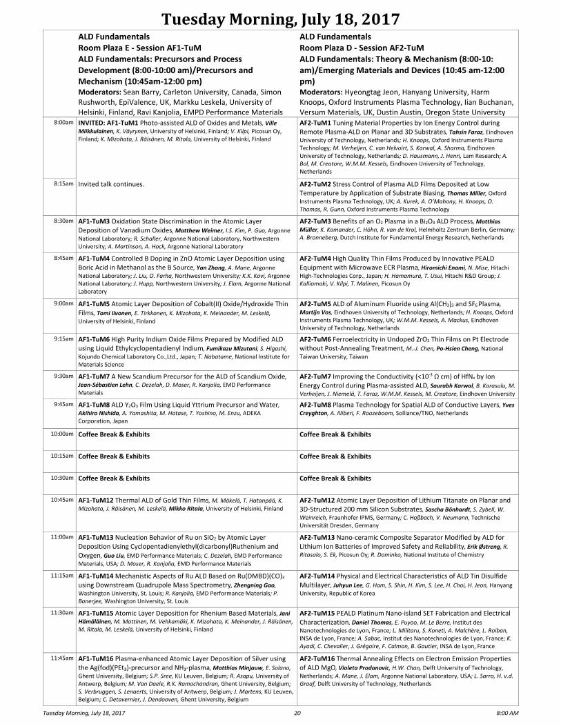
TuesdayMorning,July18,2017
Tuesday Morning, July 18, 2017 20 8:00 AM
ALD Fundamentals Room Plaza E ‐ Session AF1‐TuM ALD Fundamentals: Precursors and Process Development (8:00‐10:00 am)/Precursors and Mechanism (10:45am‐12:00 pm) Moderators: Sean Barry, Carleton University, Canada, Simon Rushworth, EpiValence, UK, Markku Leskela, University of Helsinki, Finland, Ravi Kanjolia, EMPD Performance Materials
ALD FundamentalsRoom Plaza D ‐ Session AF2‐TuM ALD Fundamentals: Theory & Mechanism (8:00‐10: am)/Emerging Materials and Devices (10:45 am‐12:00 pm) Moderators: Hyeongtag Jeon, Hanyang University, Harm Knoops, Oxford Instruments Plasma Technology, Iian Buchanan, Versum Materials, UK, Dustin Austin, Oregon State University
8:00am INVITED: AF1‐TuM1 Photo‐assisted ALD of Oxides and Metals, Ville Miikkulainen, K. Väyrynen, University of Helsinki, Finland; V. Kilpi, Picosun Oy, Finland; K. Mizohata, J. Räisänen, M. Ritala, University of Helsinki, Finland
AF2‐TuM1 Tuning Material Properties by Ion Energy Control during Remote Plasma‐ALD on Planar and 3D Substrates, Tahsin Faraz, Eindhoven University of Technology, Netherlands; H. Knoops, Oxford Instruments Plasma Technology; M. Verheijen, C. van Helvoirt, S. Karwal, A. Sharma, Eindhoven University of Technology, Netherlands; D. Hausmann, J. Henri, Lam Research; A. Bol, M. Creatore, W.M.M. Kessels, Eindhoven University of Technology, Netherlands
8:15am Invited talk continues. AF2‐TuM2 Stress Control of Plasma ALD Films Deposited at Low Temperature by Application of Substrate Biasing, Thomas Miller, Oxford
Instruments Plasma Technology, UK; A. Kurek, A. O’Mahony, H. Knoops, O. Thomas, R. Gunn, Oxford Instruments Plasma Technology
8:30am AF1‐TuM3 Oxidation State Discrimination in the Atomic Layer Deposition of Vanadium Oxides, Matthew Weimer, I.S. Kim, P. Guo, Argonne
National Laboratory; R. Schaller, Argonne National Laboratory, Northwestern University; A. Martinson, A. Hock, Argonne National Laboratory
AF2‐TuM3 Benefits of an O2 Plasma in a Bi2O3 ALD Process, Matthias
Müller, K. Komander, C. Höhn, R. van de Krol, Helmholtz Zentrum Berlin, Germany; A. Bronneberg, Dutch Institute for Fundamental Energy Research, Netherlands
8:45am AF1‐TuM4 Controlled B Doping in ZnO Atomic Layer Deposition using Boric Acid in Methanol as the B Source, Yan Zhang, A. Mane, Argonne
National Laboratory; J. Liu, O. Farha, Northwestern University; K.K. Kovi, Argonne National Laboratory; J. Hupp, Northwestern University; J. Elam, Argonne National Laboratory
AF2‐TuM4 High Quality Thin Films Produced by Innovative PEALD Equipment with Microwave ECR Plasma, Hiromichi Enami, N. Mise, Hitachi
High‐Technologies Corp., Japan; H. Hamamura, T. Usui, Hitachi R&D Group; J. Kalliomaki, V. Kilpi, T. Malinen, Picosun Oy
9:00am AF1‐TuM5 Atomic Layer Deposition of Cobalt(II) Oxide/Hydroxide Thin Films, Tomi Iivonen, E. Tirkkonen, K. Mizohata, K. Meinander, M. Leskelä,
University of Helsinki, Finland
AF2‐TuM5 ALD of Aluminum Fluoride using Al(CH3)3 and SF6 Plasma, Martijn Vos, Eindhoven University of Technology, Netherlands; H. Knoops, Oxford Instruments Plasma Technology, UK; W.M.M. Kessels, A. Mackus, Eindhoven University of Technology, Netherlands
9:15am AF1‐TuM6 High Purity Indium Oxide Films Prepared by Modified ALD using Liquid Ethylcyclopentadienyl Indium, Fumikazu Mizutani, S. Higashi,
Kojundo Chemical Laboratory Co.,Ltd., Japan; T. Nabatame, National Institute for Materials Science
AF2‐TuM6 Ferroelectricity in Undoped ZrO2 Thin Films on Pt Electrode without Post‐Annealing Treatment, M.‐J. Chen, Po‐Hsien Cheng, National
Taiwan University, Taiwan
9:30am AF1‐TuM7 A New Scandium Precursor for the ALD of Scandium Oxide, Jean‐Sébastien Lehn, C. Dezelah, D. Moser, R. Kanjolia, EMD Performance Materials
AF2‐TuM7 Improving the Conductivity (<10‐3 Ω cm) of HfNx by Ion Energy Control during Plasma‐assisted ALD, Saurabh Karwal, B. Karasulu, M.
Verheijen, J. Niemelä, T. Faraz, W.M.M. Kessels, M. Creatore, Eindhoven University
9:45am AF1‐TuM8 ALD Y2O3 Film Using Liquid Yttrium Precursor and Water, Akihiro Nishida, A. Yamashita, M. Hatase, T. Yoshino, M. Enzu, ADEKA Corporation, Japan
AF2‐TuM8 Plasma Technology for Spatial ALD of Conductive Layers, Yves Creyghton, A. Illiberi, F. Roozeboom, Solliance/TNO, Netherlands
10:00am Coffee Break & Exhibits Coffee Break & Exhibits
10:15am Coffee Break & Exhibits Coffee Break & Exhibits
10:30am Coffee Break & Exhibits Coffee Break & Exhibits
10:45am AF1‐TuM12 Thermal ALD of Gold Thin Films, M. Mäkelä, T. Hatanpää, K.
Mizohata, J. Räisänen, M. Leskelä, Mikko Ritala, University of Helsinki, Finland AF2‐TuM12 Atomic Layer Deposition of Lithium Titanate on Planar and 3D‐Structured 200 mm Silicon Substrates, Sascha Bönhardt, S. Zybell, W.
Weinreich, Fraunhofer IPMS, Germany; C. Hoßbach, V. Neumann, Technische Universität Dresden, Germany
11:00am AF1‐TuM13 Nucleation Behavior of Ru on SiO2 by Atomic Layer Deposition Using Cyclopentadienylethyl(dicarbonyl)Ruthenium and Oxygen, Guo Liu, EMD Performance Materials; C. Dezelah, EMD Performance
Materials, USA; D. Moser, R. Kanjolia, EMD Performance Materials
AF2‐TuM13 Nano‐ceramic Composite Separator Modified by ALD for Lithium Ion Batteries of Improved Safety and Reliability, Erik Østreng, R. Ritasalo, S. Ek, Picosun Oy; R. Dominko, National Institute of Chemistry
11:15am AF1‐TuM14 Mechanistic Aspects of Ru ALD Based on Ru(DMBD)(CO)3 using Downstream Quadrupole Mass Spectrometry, Zhengning Gao, Washington University, St. Louis; R. Kanjolia, EMD Performance Materials; P. Banerjee, Washington University, St. Louis
AF2‐TuM14 Physical and Electrical Characteristics of ALD Tin Disulfide Multilayer, Juhyun Lee, G. Ham, S. Shin, H. Kim, S. Lee, H. Choi, H. Jeon, Hanyang
University, Republic of Korea
11:30am AF1‐TuM15 Atomic Layer Deposition for Rhenium Based Materials, Jani Hämäläinen, M. Mattinen, M. Vehkamäki, K. Mizohata, K. Meinander, J. Räisänen, M. Ritala, M. Leskelä, University of Helsinki, Finland
AF2‐TuM15 PEALD Platinum Nano‐island SET Fabrication and Electrical Characterization, Daniel Thomas, E. Puyoo, M. Le Berre, Institut des
Nanotechnologies de Lyon, France; L. Militaru, S. Koneti, A. Malchère, L. Roiban, INSA de Lyon, France; A. Sabac, Institut des Nanotechnologies de Lyon, France; K. Ayadi, C. Chevalier, J. Grégoire, F. Calmon, B. Gautier, INSA de Lyon, France
11:45am AF1‐TuM16 Plasma‐enhanced Atomic Layer Deposition of Silver using the Ag(fod)(PEt₃)‐precursor and NH₃‐plasma, Matthias Minjauw, E. Solano,
Ghent University, Belgium; S.P. Sree, KU Leuven, Belgium; R. Asapu, University of Antwerp, Belgium; M. Van Daele, R.K. Ramachandran, Ghent University, Belgium; S. Verbruggen, S. Lenaerts, University of Antwerp, Belgium; J. Martens, KU Leuven, Belgium; C. Detavernier, J. Dendooven, Ghent University, Belgium
AF2‐TuM16 Thermal Annealing Effects on Electron Emission Properties of ALD MgO, Violeta Prodanovic, H.W. Chan, Delft University of Technology,
Netherlands; A. Mane, J. Elam, Argonne National Laboratory, USA; L. Sarro, H. v.d. Graaf, Delft University of Technology, Netherlands
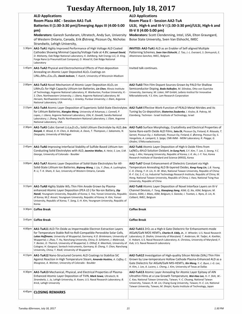
TuesdayAfternoon,July18,2017
Tuesday Afternoon, July 18, 2017 21 1:30 PM
ALD Applications Room Plaza ABC ‐ Session AA1‐TuA Batteries II (1:30‐3:30 pm)/Emerging Apps III (4:00‐5:00 pm) Moderators: Ganesh Sundaram, Ultratech, Andy Sun, University of Western Ontario, Canada, Erik Østreng, Picosun Oy, Nicholas Strandwitz, Lehigh University,
ALD ApplicationsRoom Plaza E ‐ Session AA2‐TuA ULSI, High‐k and III‐V I (1:30‐3:30 pm)/ULSI, High‐k and III‐V II (4:00‐5:00 pm) Moderators: Scott Clendenning, Intel, USA, Elton Graungard, Boise State University, Sven Van Elshocht, IMEC
1:30pm AA1‐TuA1 Highly Improved Performance of High Voltage ALD Coated Cathodes Showing Minimal Capacity/Voltage Fade at 4.8V, Lamuel David,
D. Mohanty, Oak Ridge National Laboratory; K. Dahlberg, Xalt Energy LLC; D. King, Forge Nano (a PneumatiCoat Company); D. Wood III, Oak Ridge National Laboratory
INVITED: AA2‐TuA1 ALD as an Enabler of Self‐aligned Multiple Patterning Schemes, Sven Van Elshocht, Z. Tao, J.‐L. Everaert, S. Demuynck, E.
Altamirano‐Sanchez, IMEC, Belgium
1:45pm AA1‐TuA2 Physical and Electrochemical Effects of Post‐deposition Annealing on Atomic Layer Deposited Al2O3 Coatings on LiNi0.5Mn0.3Co0.2O2, David Jackson, T. Kuech, University of Wisconsin‐Madison
Invited talk continues.
2:00pm AA1‐TuA3 Novel Mechanism of Atomic Layer Deposition Al2O3 on LiMn2O4 for High Capacity Lithium‐ion Batteries, Lin Chen, Illinois Institute of Technology; Argonne National Laboratory; R. Warburton, Purdue University; K.‐S. Chen, Northwestern University; J. Libera, Argonne National Laboratory; M. Hersam, Northwestern University; J. Greeley, Purdue University; J. Elam, Argonne National Laboratory, USA
AA2‐TuA3 Thin Film Dopant Sources Grown by PALD for Shallow Semiconductor Doping, Bodo Kalkofen, M. Silinskas, Otto von Guericke
University, Germany; M. Lisker, IHP GmbH, Leibniz‐Institut für Innovative Mikroelektronik; Y.S. Kim, Lam Research Corporation
2:15pm AA1‐TuA4 Atomic Layer Deposition of Superionic Solid‐State Electrolytes for Lithium Batteries, Xiangbo Meng, University of Arkansas; J. Connell, P.
Lopes, J. Libera, Argonne National Laboratory, USA; K. Zavadil, Sandia National Laboratory; J. Zhang, Pacific Northwestern National Laboratory; J. Elam, Argonne National Laboratory, USA
AA2‐TuA4 Effective Work‐Function of PEALD Metal Nitrides and its Tuning by Co‐deposition, Ekaterina Zoubenko, I. Krylov, B. Pokroy, M.
Eizenberg, Technion ‐ Israel Institute of Technology, Israel
2:30pm AA1‐TuA5 Cubic Garnet Li7La3Zr2O12 Solid Lithium Electrolyte by ALD, Eric Kazyak, K. Wood, K.‐H. Chen, A. Bielinski, A. Davis, T. Thompson, J. Sakamoto, N. Dasgupta, University of Michigan
AA2‐TuA5 Surface Morphology, Crystallinity and Electrical Properties of Some Rare‐earth Oxide ALD Films, Satu Ek, Picosun Oy, Finland; R. Ritasalo, T. Sarnet, Picosun Oy; J. Kalliomaki, Picosun Oy, Finland; E. Østreng, Picosun Oy; S. Vangelista, A. Lamperti, S. Spiga, CNR‐IMM ‐ MDM Laboratory; R. Piagge, G. Ghidini, STMicroelectronics
2:45pm AA1‐TuA6 Improving Interfacial Stability of Sulfide‐Based Lithium‐Ion‐Conducting Solid Electrolytes with ALD, Jasmine Wallas, A. Heist, S. Lee, S.M.
George, University of Colorado ‐ Boulder
AA2‐TuA6 Atomic Layer Deposition of High‐k Oxide Films from La(NO33∙6H2O Solution Oxidant, In‐Sung Park, S.Y. Kim, T. Lee, S. Seong, Y.C.
Jung, J. Ahn, Hanyang University, Republic of Korea; J.‐K. An, J.‐Y. Yun, Korea Research Institute of Standard and Science (KRISS), Korea
3:00pm AA1‐TuA7 Atomic Layer Deposition of Solid‐State Electrolytes for All‐Solid‐State Lithium Ion Batteries, Biqiong Wang, J. Liu, Y. Zhao, A. Lushington,
R. Li, T.‐K. Sham, X. Sun, University of Western Ontario, Canada
AA2‐TuA7 Great Enhancement of Dielectric Constant via High Temperature Annealing ALD Bi‐layered Oxides, Keng‐Yung Lin, L.B. Young, C.‐K. Cheng, Y.‐H. Lin, H.‐W. Wan, National Taiwan University, Republic of China; R.‐F. Cai, S.‐C. Lo, Industrial Technology Research Institute, Republic of China; M. Hong, National Taiwan University, Republic of China; J. Kwo, National Tsing Hua University, Republic of China
3:15pm AA1‐TuA8 Highly Stable WS2 Thin Film Anode Grown by Plasma‐enhanced Atomic Layer Deposition (PEA LD ) for Na‐ion Battery, Dip Nandi, Yeungnam University, Republic of Korea; S. Yeo, Yonsei University, Republic of Korea; M.Z. Ansari, Yeungnam University, Republic of Korea; H. Kim, Yonsei University, Republic of Korea; T. Song, S.‐H. Kim, Yeungnam University, Republic of Korea
AA2‐TuA8 Atomic Layer Deposition of Novel Interface Layers on III‐V Channel Devices, F. Tang, Xiaoqiang Jiang, ASM; Q. Xie, ASM, Belgium; M.
Givens, ASM; J. Maes, ASM, Belgium; S. Sioncke, I. Tsvetan, L. Nyns, D. Lin, N. Collaert, IMEC, Belgium
3:30pm Coffee Break Coffee Break
3:45pm Coffee Break Coffee Break
4:00pm AA1‐TuA11 ALD‐Tin Oxide as Impermeable Electron Extraction Layers for Temperature Stable Roll‐to‐Roll‐Compatible Perovskite Solar Cells, Lukas Hoffmann, University of Wuppertal, Germany; K.O. Brinkmann, University of Wuppertal; J. Zhao, T. Hu, Nanchang University, China; D. Schlamm, J. Malerczyk, T. Becker, D. Theirich, University of Wuppertal; S. Olthof, K. Meerholz, University of Cologne; H. Gargouri, Sentech Instruments, Germany; B. Cheng, Y. Chen, Nanchang University, China; T. Riedl, University of Wuppertal
AA2‐TuA11 ZrO2 as a High‐k Gate Dielectric for Enhancement‐mode AlGaN/GaN MOS HEMTs, Charles R. Eddy, Jr., V. Wheeler, U.S. Naval Research
Laboratory; D. Shahin, University of Maryland; T. Anderson, M. Tadjer, A. Koehler, K. Hobart, U.S. Naval Research Laboratory; A. Christou, University of Maryland; F. Kub, U.S. Naval Research Laboratory
4:15pm AA1‐TuA12 Nano‐Structured Ceramic ALD Coatings to Stabilize SiC Against Reaction in High Temperature Steam, Amanda Hoskins, A. Coffey, C.
Musgrave, A. Weimer, University of Colorado ‐ Boulder
AA2‐TuA12 Investigation of High‐quality Silicon Nitride (SiNx) Thin Film Grown by Low‐temperature Hollow Cathode Plasma‐Enhanced ALD as a Gate Dielectric for AlGaN/GaN MIS‐HEMTs, Xin Meng, Y.‐C. Byun, J.‐G. Lee,
H. Kim, J. Lee, A. Lucero, L. Cheng, J. Kim, University of Texas at Dallas
4:30pm AA1‐TuA13 Mechanical, Physical, and Electrical Properties of Plasma‐Enhanced Atomic Layer Deposition of TiVN, Mark Sowa, Ultratech; N.
Strandwitz, L. Ju, Lehigh University; A. Kozen, U.S. Naval Research Laboratory; B. Krick, Lehigh University
AA2‐TuA13 Atomic Layer Annealing for Atomic Layer Epitaxy of AlN Ultrathin Films at a Low Growth Temperature, Wei‐Hao Lee, H.‐Y. Shih, W.‐
C. Kao, National Taiwan University, Taiwan; Y.‐C. Chuang, National Taiwan University, Taiwan; R.‐M. Lin, Chang Gung University, Taiwan; H.‐C. Lin, National Taiwan University, Taiwan; M. Shiojiri, Kyoto Institute of Technology, Japan
4:45pm CLOSING REMARKS
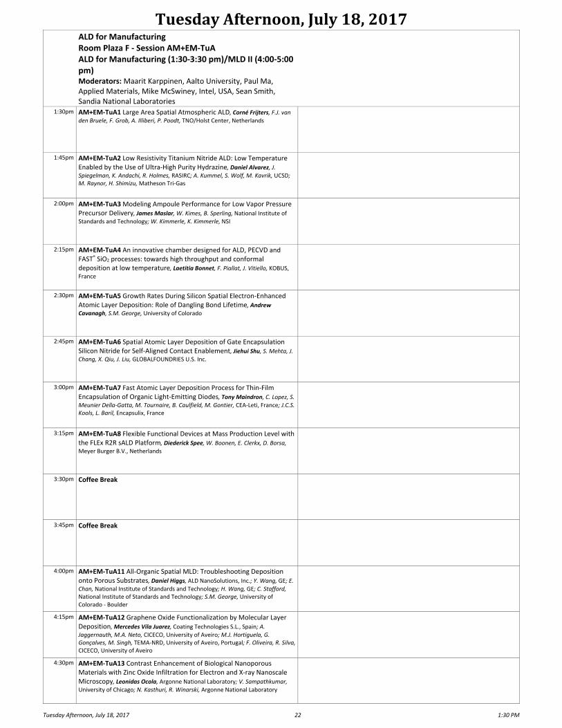
TuesdayAfternoon,July18,2017
Tuesday Afternoon, July 18, 2017 22 1:30 PM
ALD for Manufacturing Room Plaza F ‐ Session AM+EM‐TuA ALD for Manufacturing (1:30‐3:30 pm)/MLD II (4:00‐5:00 pm) Moderators: Maarit Karppinen, Aalto University, Paul Ma, Applied Materials, Mike McSwiney, Intel, USA, Sean Smith, Sandia National Laboratories
1:30pm AM+EM‐TuA1 Large Area Spatial Atmospheric ALD, Corné Frijters, F.J. van den Bruele, F. Grob, A. Illiberi, P. Poodt, TNO/Holst Center, Netherlands
1:45pm AM+EM‐TuA2 Low Resistivity Titanium Nitride ALD: Low Temperature Enabled by the Use of Ultra‐High Purity Hydrazine, Daniel Alvarez, J. Spiegelman, K. Andachi, R. Holmes, RASIRC; A. Kummel, S. Wolf, M. Kavrik, UCSD; M. Raynor, H. Shimizu, Matheson Tri‐Gas
2:00pm AM+EM‐TuA3 Modeling Ampoule Performance for Low Vapor Pressure Precursor Delivery, James Maslar, W. Kimes, B. Sperling, National Institute of
Standards and Technology; W. Kimmerle, K. Kimmerle, NSI
2:15pm AM+EM‐TuA4 An innovative chamber designed for ALD, PECVD and FAST® SiO2 processes: towards high throughput and conformal deposition at low temperature, Laetitia Bonnet, F. Piallat, J. Vitiello, KOBUS, France
2:30pm AM+EM‐TuA5 Growth Rates During Silicon Spatial Electron‐Enhanced Atomic Layer Deposition: Role of Dangling Bond Lifetime, Andrew
Cavanagh, S.M. George, University of Colorado
2:45pm AM+EM‐TuA6 Spatial Atomic Layer Deposition of Gate Encapsulation Silicon Nitride for Self‐Aligned Contact Enablement, Jiehui Shu, S. Mehta, J.
Chang, X. Qiu, J. Liu, GLOBALFOUNDRIES U.S. Inc.
3:00pm AM+EM‐TuA7 Fast Atomic Layer Deposition Process for Thin‐Film Encapsulation of Organic Light‐Emitting Diodes, Tony Maindron, C. Lopez, S.
Meunier Della‐Gatta, M. Tournaire, B. Caulfield, M. Gontier, CEA‐Leti, France; J.C.S. Kools, L. Baril, Encapsulix, France
3:15pm AM+EM‐TuA8 Flexible Functional Devices at Mass Production Level with the FLEx R2R sALD Platform, Diederick Spee, W. Boonen, E. Clerkx, D. Borsa,
Meyer Burger B.V., Netherlands
3:30pm Coffee Break
3:45pm Coffee Break
4:00pm AM+EM‐TuA11 All‐Organic Spatial MLD: Troubleshooting Deposition onto Porous Substrates, Daniel Higgs, ALD NanoSolutions, Inc.; Y. Wang, GE; E.
Chan, National Institute of Standards and Technology; H. Wang, GE; C. Stafford, National Institute of Standards and Technology; S.M. George, University of Colorado ‐ Boulder
4:15pm AM+EM‐TuA12 Graphene Oxide Functionalization by Molecular Layer Deposition, Mercedes Vila Juarez, Coating Technologies S.L., Spain; A.
Jaggernauth, M.A. Neto, CICECO, University of Aveiro; M.J. Hortiguela, G. Gonçalves, M. Singh, TEMA‐NRD, University of Aveiro, Portugal; F. Oliveira, R. Silva, CICECO, University of Aveiro
4:30pm AM+EM‐TuA13 Contrast Enhancement of Biological Nanoporous Materials with Zinc Oxide Infiltration for Electron and X‐ray Nanoscale Microscopy, Leonidas Ocola, Argonne National Laboratory; V. Sampathkumar,
University of Chicago; N. Kasthuri, R. Winarski, Argonne National Laboratory