Embed Size (px)
Citation preview

Dept. of Electrical Engineering
Analog and Mixed-Signal
Design for SOC
大同大學電機系
黃淑絹副教授

2
Outline
Analog and Mixed-Signal Design in the SOC EraCurrent Mirrors and Biasing CircuitsSingle-Stage AmplifiersOperational AmplifiersLayout of Analog and Mixed-Signal ICs

3
ITRS
International Technology Roadmap for Semiconductors (http://public.itrs.net)Minimum Gate Length for Digital Transistors
Gate Length Projections
0
10
20
30
40
50
60
70
80
90
100
2001 2003 2005 2007 2009 2011 2013 2015
Leng
th in
nm

4
ITRS (cont.)
Supply Voltages for Digital and Analog ICsSupply Voltage Projections
0
0.5
1
1.5
2
2.5
3
3.5
2001 2003 2005 2007 2009 2011 2013 2015
Vol
tage
Analog Supply Range
Digital Supply Voltage

5
ITRS (cont.)
“The mixed-signal supply voltage continues to lag that of high-performance digital by two or more generations. A combination of multiple gate oxide thickness, multiple thresholds, and DC-DC conversion is needed to support the increased mixed-signal requirements. Solutions in active threshold regulation, substrate biasing, and novel design architecture will be required to extend the trend for lower supply voltages for mixed-signal applications. An alternative to full integration is the SIP that combines circuits made with different technologies and optimized for the desired functions. We expect that full-digital implementations in CMOS will replace most analog functions except for analog-to-digital conversion (ADC).”

6
Challenges for AMS designers
Major Issuesgm and go are both degrading. ⇒ difficult to build high gain amplifiers.Feedback is difficult to use.Signal swing is decreasing with VDD. ⇒ difficult to get acceptable SNRMany existing architectures will not functionGates are leaking. ⇒ Charge redistribution circuits may not workDevices becomes increasingly nonlinear. ⇒ Spectral performance of many circuits will degrade.Many existing architectures will not give acceptable performance.Matching is becoming worse. ⇒ difficult to obtain acceptable soft yieldsPerformance expectations are increasing.Increased mask and processing costsIncreased concerns about AMS test

7
AMS design in SOC
Increasing need for data converters Oversamped for low-frequency high resolutionNyquist rate structures for higher speeds
Feedback will be even more important in high spectral purity applications.Design for yield will become essential.New circuit architectures that operate at low voltages will become essential.

8
Outline
Analog and Mixed-Signal Design in the SOC EraCurrent Mirrors and Biasing CircuitsSingle-Stage AmplifiersOperational AmplifiersLayout of Analog and Mixed-Signal ICs

9
MOS Transistors
CMOS N-Well Process
Common Used Symbols NMOS
PMOS
G G
SiO2
p-subtrate
S DB D S B
PMOSNMOS
gateoxide
polyfieldoxide
p+ n+ n+
n-well
n+p+p+ SiO2SiO2
VSSVDD
G
D
S
B
GB
S
D

10
MOS Transistors (cont.)
Important Dimensions of a MOS Transistor
L: Channel lengthW: Channel widthtox: oxide thicknessCapacitance
W
tox
e)capacitanc (gate
area)unit per ecapacitanc (oxide
WLCCt
C
OXG
OX
OXOX
=
=ε

11
MOS Transistors (cont.)
Drain Current Equation in Saturation RegionIncluding channel-length modulation and body Effects
2
212
2
( ) (1 )
where (L )Ksi oqN A
DS eff B
WD n OX GS tn DSL
L V V
I C V V Vε
µ λ
λ λ− +Φ
= − +
= ↑ ⇒ ↓
)|2||2|(
)( and | where
)|2||2|(2
120
FFBStpotp
CqN
Vtntno
FFSBtnotn
VVV
VVV
VVV
OX
siSUB
SB
Φ−Φ+−=
==
Φ−Φ++=
=
γ
γ
γε

12
Small-Signal Model
Linear ComponentsLinear Resistor
Linear Capacitor
Dependent Circuits
RIV =
CVQ =
(CCVS) (CCCS) (VCVS) (VCCS)
12
12
12
12
rIVIIVV
gVI
====
βα
The slope corresponds to resistance, conductance, capacitance, transconductance, etc.
y
x
slope

13
Small-Signal Model (cont.)
Linear Approximation for Nonlinear Components
xdx
xdyxyxyy
xxx
xxdx
xydxxdx
xdyxyxy
∆≈−=∆
−=∆
+−+−+=
)()()(
, smallFor
)()()()()()(
00
0
202
02
00
0 L
y 1. Find the operation point.2. Determine the slope,
which determine the value for the linear component.
3. Remove the DC bias, and replace the device with the linear components.
dxxdy )( 0∆y
∆xy0
xx0

14
MOS Small-Signal Model
gmvgs
+vgs
-
G
S
Drdsgmbvbs
+vbs
-B
tnGS
DDOXntnGSOXnQ
GS
Dm VV
IIL
WCVVL
WCvig
−==−=
∂∂
=22)( µµ
|2|1
2
)|2||2|(
||22
FSBBS
tn
FFSBtnotn
mFSB
m
BS
tn
tn
DQ
BS
Dmb
VvV
VVV
gV
gvV
Vi
vig
Φ+−=
∂∂
Φ−Φ++=
=+
=∂∂
∂∂
=∂∂
=
γγ
ηφ
γD
DS
Ddsds I
vigr λα =
∂∂
=== −1

15
MOS Device Capacitances
Variation of CGS and CGD versus VGS
Saturation region
channel theoadjacent t side theexcluding perimetersdrain and source :,
areasdrain and source :,
)(
cap.) (overlap 32
ds
ds
swjdjdddb
swjsjsssb
OVOXgd
OVOXOXgs
PPAA
CPCAC
CPCWLAC
WLCC
WLCWLCC
−
−
+=
++=
=
+=
fixed

16
MOS Device Capacitances (cont.)
Triode region
Cut-off regionswjdjdddb
swjsjsssb
OVOXOXgd
OVOXOXgs
tnGSOXnDS
Ddsds
CPCWLAC
CPCWLAC
WLCWLCC
WLCWLCC
VVL
WCVIgr
−
−
−
++=
++=
+=
+=
−≅∂∂
==
)(
)(
)(
21
21
21
21
1 µ
deplOX
deplOXgb
swjdjdddb
swjsjsssb
OVOXgd
OVOXgs
CWLCCWLC
C
CPCAC
CPCAC
WLCC
WLCC
+=
+=
+=
=
=
−
−

17
Basic Current Mirrors
MOSFETs as Current SourceBiasing in saturation with a fixed gate voltage
Using resistive divider to provide the gate voltage
)1()(21 2
21
2
efftnbOXnout
DDb
VVVL
WCI
VRR
RV
λµ +−=
+= Sensitivity to
supply, process and temperature

18
Basic Current Mirrors (cont.)
Current Copiers
Diode-Connected device providing inverse functionAssume λ=0.
)(
)(1
REFGS
GSD
IfV
VfI−=
=
Current Mirror
REFout
tnGSOXnout
tnGSOXnREF
ILWLWI
VVL
WCI
VVL
WCI
1
2
22
21
)/()/(
)()(21
)()(21
=
−=
−=
µ
µ

19
Errors in Current Mirrors
Simple Current Mirror
Output resistance
Iout
+
-
Vout
Iin
M1 M2+-VGS
ineff
effout
efftnGS
IVV
LWLWI
VVV
×+
+=
=−≥
1
2
1
2
out
11
)/()/(
V:region saturationin M2
λλ
2dsout rR =
Μ1 Μ2

20
Cascode Current Mirror
Suppressing Channel-Length Modulation Effect⇒cascode structure
Output Resistance
0
1
mg
1
1
mg2dsr
3dsr233 )( dsdsmout rrgR ≈

21
Cascode Current Mirror (cont.)
Head-room consumed by a cascode mirror
1103
11
00
10 )/(2
)/(2
tneffefftnNout
tnOXn
REFtn
OXn
REFGSGSN
VVVVVV
VLWC
IVLWC
IVVV
++=−≥
+++=+=µµ
1
500M 1.50 2.50 3.50 4.50Vout (V)
120U
80.0U
40.0U
0
-40.0UIo
ut(A
)
simplecascode

22
Cascode Current Mirror (cont.)
Minimum headroom voltage
tnGSb VVV −= 2 GSb VV 2=

23
Low-Voltage Cascode Current Mirror
Modified of Cascode CM for Low-Voltage (Wide-Swing) Operation
212
21121
21121
121112
2121
:saturationin M1
:saturationin M2
tntnGS
tnGStnGSGS
tnGSbtnGSGS
tnGSGSbtnGSGSbA
tnGSbtnbGSX
VVVVVVVV
VVVVVVVVVVVVVVV
VVVVVVV
≤−⇒+≤−+⇒
+≤≤−+⇒−+≥⇒−≥−=
+≤⇒−≥=
212
211 )(
effefftnbout
GStnGSb
VVVVVVVVV
+=−≥⇒
+−=
24
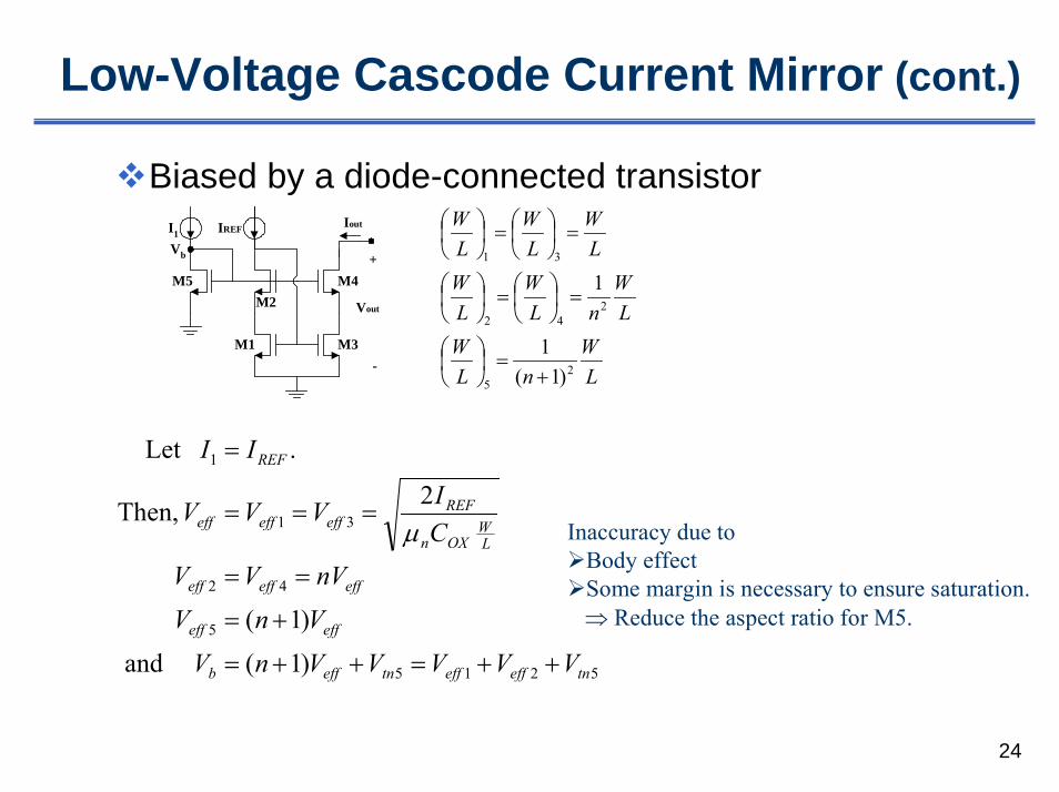
Low-Voltage Cascode Current Mirror (cont.)
Biased by a diode-connected transistor
LW
nLW
LW
nLW
LW
LW
LW
LW
25
242
31
)1(1
1
+=
=
=
=
=
IREF Iout
+
-
Vout
M3M1
M4M2
I1
Vb
M5
5215
5
42
31
1
)1( and
)1(
2 Then,
.Let
tneffefftneffb
effeff
effeffeff
LW
OXn
REFeffeffeff
REF
VVVVVnV
VnV
nVVVCIVVV
II
++=++=
+=
==
===
=
µ Inaccuracy due toBody effectSome margin is necessary to ensure saturation.⇒ Reduce the aspect ratio for M5.

25
Low-Voltage Cascode Current Mirror (cont.)
Design for short-Channel Devices

26
Regulated Drain Current Mirror

27
Supply-Independent Bias
Supply-Dependent BiasingResistive Bias
Example
golden referencecurrent
VDD
IREF
M1 M2
Iout
VDD
IREF
M1 M2
IoutR1
DD
1
2
11
V tosensitive
)/()/(
/1⇒
+∆
=∆LWLW
gRVI
m
DDout

28
Supply-Independent Biasing (cont.)
Using MOSFET only
tppOXp
REFtn
nOXn
REFDD V
LWCIV
LWCIV −++=
)/(2
)/(2
µµ
29
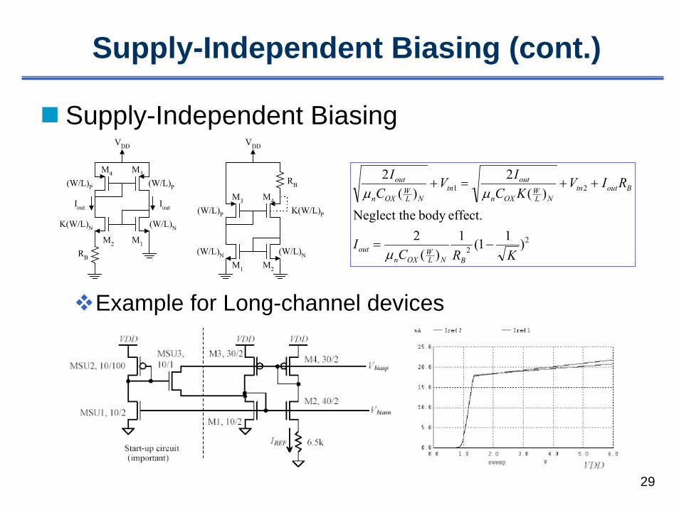
Supply-Independent Biasing (cont.)
Supply-Independent Biasing
Example for Long-channel devices
22
21
)11(1)(
2effect.body eNeglect th
)(2
)(2
KRCI
RIVKCIV
CI
BNLW
OXnout
BouttnNL
WOXn
outtn
NLW
OXn
out
−=
++=+
µ
µµ
VDD
RB
M1
M3
M2
M4
K(W/L)N (W/L)N
(W/L)P (W/L)P
IoutIout
VDD
M1 M2
M3 M4
(W/L)N (W/L)N
(W/L)P K(W/L)P
RB

30
Supply-Independent Biasing (cont.)
Short-Channel Device

31
Supply-Independent Biasing (cont.)
Using feedback to increase the output resistance of MOSFET

32
Supply-Independent Biasing (cont.)
Improved circuit

33
Outline
Analog and Mixed-Signal Design in the SOC EraCurrent Mirrors and Biasing CircuitsSingle-Stage AmplifiersOperational AmplifiersLayout of Analog and Mixed-Signal ICs

34
Common-Source Amplifier
Common-Source Amplifier
+
-VIN
M3 M2
M1CL
RIN
Vout
VDD
Ibias
Rout
outR
212
21 //
dbdbL
dsdsout
CCCCrrR
++==
++≅++=
++≅
++++≅
−=
−
21121
222111
112
211113
10
1)1)(1()(
)()]1([1
ppppp
gdgsgsgd
gdmp
gdoutoutmgdgsindB
outmv
sssssD
CCCCCCCg
CCRRgCCR
RgA
ωωωωω
ω
ω
)(
)()]1([where
1)1(
222111
21111
21 1
1
CCCCCCRRb
CCRRgCCRa
bssasRg
VV
gdgsgsgdoutin
gdoutoutmgdgsin
gC
outm
in
out m
gd
++=
++++=
++
−−=

35
Common-Source Amplifier (cont.)
Miller’s Theorem
Miller Capacitance
-3dB Frequency open-circuit time constant method
Y
Y1
+V1-
+V2-
Y1
+V1-
+V2-
I1 I1I2 I2
K=V2/V1
222122
111211
)11()(
)1()(
YVYK
VYVVI
YVYKVYVVI
=−=−=
=−=−=
neglected)(usually )11(
Capacitor)(Miller
)1()1(
11
11
111
10
gdgdright
gdoutm
gdoutmgdleftM
outmv
CCK
C
CRg
CRgCKCCRgAK
≈−=
≈
+=−==−==
YK
Y
YKY
)11(
)1(
2
1
−=
−=
)(][11
213 CCRCCRCR rightoutMgsin
iii
dB +++≈≅
∑−ω

36
Source Follower
Source-Follower
No voltage gainLow output resistanceNot suffering from Miller effect ⇒ better frequency responseExhibiting large amounts of overshoot and ringing under certain conditions
+
-VIN
M3 M2
M1
CL
Rin
Vout
VDD
IbiasRout
Vin
Vout
Rin
Cgs1
Cgd1
gm1Vgs1 gs1Vs1
rds1
rds2 C2
+Vgs−
Vin
Vout
Rin
Cgs1Cgd1gm1Vgs1
R2 C2
+Vgs−
212
1212 )/1(||||
dbsbL
sdsds
CCCCgrrR
++==
1
/1)()/1(||
2111
110
11
211112
<+++
==
≅+++== −
dsdssm
moutmv
mdsdssmmout
gggggRgA
ggggggRR

37
Common-Gate Amplifier
Common-Gate Amplifier
The gain is slightly less than that of the common-source amplifier.Since the gate of the transistor is ac ground, it does not suffer from Miller effect.
⇒ Frequency response is superior to that of CS amplifier.
M3 M2
M1 CL
Vout
VDD
Ibias
RS
+
-VIN
Vbias
rin
Rout
1
1
1
1
12
11111
1
1
111
1
)2 ,For ( )1(11
dsL
m
inS
in
s
out
in
s
in
out
mindsL
ds
L
mdssm
Ldsin
dsL
dssm
s
out
gGg
rRr
VV
VV
VV
grrR
rR
ggggRgr
gGggg
VV
+×
+≅=
≈=+≅++
+=
+++
=

38
Cascode Amplifier
Cascode Amplifier
Folded-Cascode Amplifier⇒ improving input range
M5
M2
M1
CL
Vout
VDD
Ibias
Rin
+
-VIN
Vbias
Ron
M3
M4
M6Rop
outmv
oponout
dsdsmop
dsdsmon
RgA
RRRrrgRrrgR
−=
=
≅≅
0
433
122
||
LoutdB
outin
CR
RR
1.resistanceoutput large its todue poleoutput by the
dominantususally isfrequency 3dB- the,For
3 ≈
<<
−ω

39
Differential Amplifier
Differential Pair
M1 M2
iD1 iD2
2.5VvI1
iB

40
Differential Amplifier (cont.)
Current Mirror Load -- Large-Signal Analysis
I∆+ I∆−I∆+
SSI0
↓↓
0
0=outV
↓
)( 21 ininout VVfV −=
IISS ∆−2 IISS ∆+
2
IISS ∆−2
↑
)( 21 ininout VVfV −=
IISS ∆+2 IISS ∆−
2
IISS ∆+2
SSI 0
↑↑
DDout VV =
SSI
M1, M3, M4: offM2, M5: deep triode
M2: offM4: deep triode

41
Differential Amplifier (cont.)
I/O Characteristic
Vout vs. VDD
↑
↓
↑
Fout VV =circuit, symmetricFor

42
Differential Amplifier (cont.)
Small-Signal Analysis Asymmetric Swings due to the Load
Calculation of Gm
1
121 22
min
outm
inmin
min
mout
gviG
vgvgvgi
−==
−=−−=

43
Differential Amplifier (cont.)
Calculation of Rout
Overall Gain
4or1XI
42
42,143
32,1
//
//122
ooout
o
X
o
X
o
X
om
o
XX
rrR
rV
rV
rV
rg
r
VI
≈
+≈++
=
outR 2C
23
10
422
42
1
//
CR
RgACCCC
rrR
outdB
outmv
dbdbL
dsdsout
≈
≈++=
=
−ω
biasMds
biasMds
biasLW
OXnm
Ir
Ir
ICg
44
22
1
2
2
λ
λ
µ
=
=
=+
-Vin
Vout
M1 M2
M4M3
Ibias
CL

44
Differential Amplifier (cont.)
Single-Ended vs Differential Amplifier
For given device dimension, this circuit requires half of the bias current to achieve the same gain as a differential pair. However, advantages of differential operation often outweigh the power penalty.
)//( 211 oomv rrgA −=

45
Differential Amplifier (cont.)
Power-Supply Rejection Ratio (PSRR)
PSRR+
PSRR-
+ −
VB1
Vo
M1
M3 M4
M2
M5
VDD
VSS
CL
1/gm3
2ro2
i
vo
i ro4
vdd
CL
Loop
p
vd
pdd
odd
Crr
sAA
svvA
)//(1
/1
/11
42
0
=
+=
+==
ω
ω
ω0|| 1 v
dd
ddd A
AAPSRRA ==⇒= +
mismatches toduemainly ||
0
⇒∞→=
==
−ss
d
ss
oss
AAPSRR
vvA

46
Systematic Design Approach
Parameter Domains for Characterizing Amplifier Performance
Degrees of Freedom: 2Small-signal parameter domain
Natural design parameter domain
Alternate parameter domain
L
momv C
gGBrgA =−= 1
, om rg
DOXn
D
OXnv ILW
CGB
ILWC
A /2
/2
=
−=
λµ
λµ
EBLDDEBv V
PCV
GBV
A
=
−=
2 12λ
,/ DILW
, EBVP
47
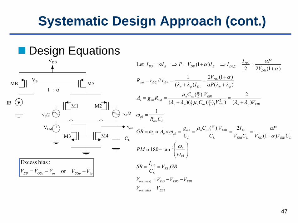
Systematic Design Approach (cont.)
Design Equations
+−
voutVCM
vd/2 -vd/2
VB
VDD
M1 M2
M5MB
IB
M3 M4
1 : α
CL
3(min)
15(max)
15
1
1
11
11111
1
12
1121
111
142
52,15
tan180
)1(2)(
1)(
2))()((
)(
)()1(2
)(1//
)1(22 )1( Let
EBout
EBEBDDout
EBL
D
p
t
LEBDDLEB
D
L
EBLW
oxn
L
mpvt
Loutp
EBpnEBLW
oxnpn
EBLW
oxnoutmv
pn
DD
Dpndsdsout
DD
DDBDDBD
VVVVVV
GBVCISR
PM
CVVP
CVI
CVC
CgAGB
CR
VVCVCRgA
PV
IrrR
VPIIIVPII
=
−−=
==
−≈
+====×≈=
=
+=
+==
++
=+
==
+==⇒+=⇒=
−
ωω
ααµωω
ω
λλµλλµ
λλαα
λλ
αααα
tpSGptnGSnEB VVVVV +−= or :bias Excess

48
Systematic Design Approach (cont.)
Input Common-Mode Range (CMR)
CMR+For M5 in the saturation region,
CMR-For M1 in the saturation region,
11515
5(min)5
tpEBEBDDSGEBDDCM
EBSD
VVVVVVVV
VV
−−−=−−=
=
+
13313
3111111
tptnEBtpGSCM
GStpDGtpSGSD
VVVVVV
VVVVVVV
++=+=
=+≥⇒+≥
−
49
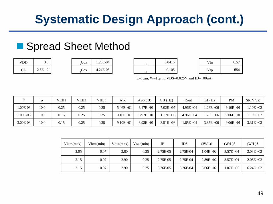
Systematic Design Approach (cont.)
Spread Sheet Method
3.31E+029.06E+013.85E+061.65E+043.51E+083.92E+019.10E+010.25 0.25 0.15 10.0 3.00E-03
1.10E+029.06E+011.28E+064.96E+041.17E+083.92E+019.10E+010.25 0.25 0.15 10.0 1.00E-03
1.10E+029.10E+011.28E+064.96E+047.02E+073.47E+015.46E+010.25 0.25 0.25 10.0 1.00E-03
SR(V/us)PMfp1 (Hz)RoutGB (Hz)Avo(dB)AvoVBE5VEB3VEB1αP
L=1µm, W=10µm, VDS=0.825V and ID=100uA
-0.754Vtp0.105λp4.24E-05μpCox2.5E-12CL
0.57Vtn0.0415λn1.23E-04μnCox3.3VDD
6.24E+021.07E+028.66E+028.26E-048.26E-050.25 2.90 0.07 2.15
2.08E+023.57E+012.89E+022.75E-042.75E-050.25 2.90 0.07 2.15
2.08E+023.57E+011.04E+022.75E-042.75E-050.25 2.80 0.07 2.05
(W/L)5(W/L)3(W/L)1ID5IBVout(min)Vout(max)Vicm(min)Vicm(max)

50
Outline
Analog and Mixed-Signal Design in the SOC EraCurrent Mirrors and Biasing CircuitsSingle-Stage AmplifiersOperational AmplifiersLayout of Analog and Mixed-Signal ICs

51
Ideal Opamps and Applications
Ideal Opamp
Open Loop
∞→∞→
→∞→
BWARR
o
id
0-
+
VoutVin-
Vin+
Rid Ro
A
)( −+ −= ININOUT VVAV
−
+VINVOUT VIN
VOUT
L+
L-
slope=A

52
Ideal Opamps and Applications (cont.)
Close Loop with Negative Feedback
Inverting amplifier
Finite open-loop gain
−
+
R1
R2
VINVOUTvirtual
short 1
2
21
RR
VV
RV
RV
IN
OUT
OUTIN
−=⇒
−=
−
+
R1
R2
VINVOUT
AVOUT− A
RRR
RV
VR
VA
V
RA
VV
IN
OUT
OUTOUTOUT
IN
/)1(1
1
1
21
2
21
++×−=⇒
−=
+
.0 feedback, negative and For =−∞→
=−
−+
−+
ININ
OUTININ
VVAA
VVV

53
Ideal Opamps and Applications (cont.)
Non-inverting amplifier
Difference amplifier
−
+VIN
VOUT
R2
R1
1
2
21
1RR
VV
RVV
RV
IN
OUT
OUTININ
+=⇒
−=
−
−
+VIN
VOUT
R2
R1
AVV OUT
IN −
ARRR
RV
VR
VA
VV
RA
VV
IN
OUT
OUTOUT
INOUT
IN
/)1(1
1)1(
)()(
1
21
2
21
++×+=⇒
−−=
−−
Finite open-loop gain
−
+
V1VOUT
R2
R1
R3
R4
V2
)(
, and For
)1(
121
2
4231
11
22
1
2
43
4
VVRRV
RRRR
VRRV
RR
RRRV
OUT
OUT
−=
==
−++
=

54
Stability
General ConsiderationsBasic negative-feedback system
Example
1. anddependent in frequency is Assume)()( :gain Loop
)(1)()(
≤=
+=
βββ
βsHsL
sHsHs
XY
−
+VIN
VOUT
R2
R1
.11 ,1 If
/)1(1
1)1()/(11
/11
1
2
1
21
2
21
1
RR
VVA
ARRR
RAA
AV
VRR
R
IN
OUT
IN
OUT
+=≈>>
+++=
+=
+=⇒
+=
ββ
ββ
ββ

55
Stability (cont.)
Barkhausen’s Criteria for oscillation
Example
δω
ω
ωωωωω
ω
+=⇒=
=⇒
=−⇒=∠
−++
−=
+++
−=+
+−=
2/ 1|)(|
1
0)/(1180)()]/(1[3
/1)(
)/(13/1)1()(
120
0
000
12
12
1
2
RRjLRC
CRCRjLCRCRj
RRjL
sCRsCRRR
ZZZ
RRsL
sp
p
o
.at oscillates system The180)(
1|)(|
00
0
ωω
ω
⇒−=∠
=ojL
jL

56
Stability (cont.)
Bode plot of loop gain for unstable and stable system
o180−ω dB0ω
o180−ω
phase excess 180)(
gain excess 1|)(| if unstable, is System
0
180o
o
−<∠
>−
dBjL
jL
ω
ωo
o
180)(
1|)(| if stable, is System
0
180
−>∠
<−
dBjL
jL
ω
ω
(PX)point crossover phase :(GX)point crossover gain :
180
0
o−ωω dB

57
Stability (cont.)
Time-domain responses versus the pole locationstjjp pppp )exp( ωσωσ +⇒+=
RHP polesUnstable with growing amplitudes
Imaginary polesUnstable with constant-amplitude oscillation
LHP poles ⇒ stable

58
Stability (cont.)
One-pole systemLoop Locus
00 )1( ωβAp +−=
])1/[(11)(
/1)(
00
0
0
0
0
ωββ
ω
AsA
A
sXY
sAsH
+++
=
+=
⇒unconditional stable

59
Stability (cont.)
Multipole SystemsTwo-pole system
21
221
01
2102
21
2121
2102
21212,1
210212
210
021
0
21
0
4)(1
0)1(4)(
2
For
2)1(4)()(
)1()(
)/1)(/1()(
)/1)(/1()(
pp
pp
pppp
pp
pppppp
pppp
pp
pp
pp
A
A
pp
Ap
AssA
AssAs
XY
ssAsH
ωωωω
β
ωωβωω
ωω
ωωβωωωω
ωωβωωωω
βωω
ωω
−=⇒
=+−+⇒
+−==
+−+±+−=
++++=
+++=
++=
⇒still unconditional stable

60
Stability (cont.)
Three-pole system
Additional poles (and zeros) impact the phase to a much greater extend than they do the magnitude.If the feedback factor decreases, the circuit becomes more stable because the gain crossover move toward the origin while the phase crossover remains constant.
↓β

61
Stability (cont.)
Phase Margin
|)(|log20(PM)Margin Gain 180)((PM)Margin Phase
180
0
o
o
−−=
+∠=ω
ωjL
jL dB
o
o
180)(
1|)(| if stable, is System
0
180
−>∠
<−
dBjL
jL
ω
ω
Small PM Large PMpeaking large 5.11|)(|
)175exp(1/1
)(/11/1
)(1)()(
5180)((PM)Margin Phase
)175exp()(
175)(
0
00
00
0
0
0
⇒=
+=
+=
+=
=+∠=
−=⇒
−=∠
βω
βω
βωβ
ωω
ω
ωβ
ω
dB
dBdB
dBdB
dB
dB
dB
jXY
j
jLjHjHj
XY
jL
jjH
jL
o
oo
o
o

62
Stability (cont.)
45° phase margin
peak %03 3.1|)(|
707.0293.0/1
)135exp(1/1)(
45180)((PM)Margin Phase
)135exp()( 135)(
0
0
0
00
⇒=
+=
+=
=+∠=
−=⇒−=∠
βω
ββω
ω
ωβω
dB
dB
dB
dBdB
jXY
jjj
XY
jL
jjHjL
o
oo
oo

63
Stability (cont.)
Closed-loop time response for various phase margin
PM=60°, ⇒negligible frequency peaking⇒little ringing and fast settling
Example: unity-gain buffer (large-signal step response)
βω 1|)(| 0 =dBj
XY
Optimum value
(W/L)=50 µm /0.6µmft=150 MHzPM=65°Nonlinearity of the circuit causes the variation of the poles and zeros during transient.

64
Practical Design Parameters
ssssddddcmcmOSdvout vsAvsAvsAVvsAV )()()())(( ++++=
Gain and bandwidth (gain-bandwidth product)Phase margin Slew rate and settling timeOffset voltageCommon-mode range (CMR)Common-mode rejection ratio (CMRR)Power-supply rejection ratio (PSRR)
||cm
v
AACMRR =
||
||
ss
v
dd
v
AAPSRR
AAPSRR
=−
=+

65
Practical Design Parameters (cont.)
Linear Settling Timedue to the finite unity-gain frequency of the opamp
+ A(s)
β
Vin Vout
Vstep
ττ
τ
6.9 accuracy 0.1% 4.6 accuracy 1%
)1()(
)( )()(
: Response Step
/
⇒⇒
−=
=⇒=
−tstepout
stepinstepin
eVtvs
VsVtuVtv
occurs. limiting rate-slew no , If
| 0
SlopeSR
Vdt
dVSlope stept
out
>
== = τt
CL
ttp
pp
ssAsAsA
ssAω
AsAsA
βωββ
ωωω
ωωω
+≅
+=
≈<<<<
≈+
=
/111
)(1)()(
:gain loop-Closed
.)( ,For
) :(Note )/1(
)(
:opamp dcompensate pole-dominant a of modelorder -first Simple
1
10t1
0
tCLA βωτ
ωβ
≅=≅∴1 and 1 3dB-0

66
Practical Design Parameters (cont.)
Example: Opamp Gain and Unity Gain Frequency for an ADC
β
β
ββ
ββ
β
1
1
2
(0.5LSB) 2
11
)11(1)/(11
111
+
+
>
<
−≈
+=
+=
N
OL
NOL
OL
v
OL
OLCL
A
A
A
A
AAA
MHzfMHzf
fNtNf
ft
VVAN
CCCC
C
tCLK
CLKsettle
tCLK
settle
Nv
FI
FI
F
572 100
)1(44.0)1(11.0 ,2
1 If
(84dB) / 22 12
5.0 ,For 142
=⇒=
+=⋅
+>=
=>⇒=
==+
=
+
β
β
β
settlesettle
N
t
t
NN
settle
Nt
t
tdB
tfinaloutout
tN
tf
t
e
eVv
settle
⋅+
=⋅
>
=⋅<
<∆
==
−=
+
++
+−
−
−
βπβ
βωτ
ωβωω
τ
τ
τ
)1(11.02
2ln
2ln2ln
21 ,
2 within settle To
opamp) offrequency gain -unity :(
11
)1(
1
11
1/
3
/,

67
Telescopic Opamp
Design Equations
75(min)
319(max)
19
1
1
11
11111
1
162
42
162
42
111
62
42
162
42
866244
92,19
tan180
)1(2)(
1
)(4
)(/4
)()1(4
)(2
)(||)()1(22
)1( Let
EBEBout
EBEBEBDDout
EBL
D
p
t
LEBDDLEB
D
L
EBLW
oxn
L
mpvt
Loutp
EBEBnEBpDEBnEBp
EBDoutmv
EBnEBp
DD
DEBnEBp
dsdsmdsdsmout
DD
DDBDDBD
VVV
VVVVV
GBVCISR
PM
CVVP
CVI
CVC
CgAGB
CR
VVVIVVVIRgA
VVPV
IVV
rrgrrgRV
PIIIVPII
+=
−−−=
==
−≈
+====×≈=
=
+=
+==
++
=+
=
≅+
==⇒+=⇒=
−
ωω
ααµ
ωω
ω
λλλλ
λλαα
λλ
αααα
vout
VB
VDD
M1 M2
M9MB
M3 M4
1 : α
CL
V1 V2
VB1
VB2
M5 M6
M7 M8
EBD
EBDdsm λVI
VIrg 1 /2==
λ

68
Folded-Cascode Opamp
Design Equations
-
+Vin
Q1 Q2
Ibias
VB1Vout
Q9Q10
Q6 Q5
Q7Q8
VB2
CL Rout
consuming more powerwider ICMRslightly larger output swing
10863
113
3
10
10883166
~ :swingOutput
1
)(||)]||([
effeffeffeffDD
GSeffbtneffDD
LoutdB
outmv
dsdsmdsdsdsmout
VVVVV
VVCMRVVVCMRCR
RgArrgrrrgR
+−−
+=−+−=+
≅
≅≅
−ω

69
Folded-Cascode Opamp (cont.)
Bias Currents and Slew Rate
Ibias2/2
Ibias1
2/21 biasbias II −
offIbias2
Ibias11biasI
0
2/21 biasbias II >
L
bias
CISR 1=
offIbias2
Ibias11biasI
21 biasbias II −121 2 biasbiasbias III <≤
L
bias
L
biasbiasbias
CI
CIIISR 2211 )(
=−−
=
12 biasbias II ≤
Case 1
Case 2

70
Folded-Cascode Opamp (cont.)
Purposes for Q11 and Q12Q11 and Q12 are turned off during normal operation and almost have no effect on the opamp.Q11 and Q12 act as clamp transistors to prevent the drain voltages Q1 and Q2 from having large transients where they change from their small-signal voltages to voltages very close to the negative power-supply voltage. Thus, the opamp can recover more quickly following a slew-rate condition.Increase the slew-rate performance of the opamp:
L
bias
biasbiasbias
CISR
III
2
121 2
=
<≤

71
Folded-Cascode Opamp (cont.)
Design Example
95.3 19.6 9.5 3.3 9.5 74.4 W/L
126.26 75.76 12.63 12.63 12.63 63.13 ID (µA)
M11M9M3M7M5M1
14.69 0.50 2.80 -0.50 2.10 7.58 126.26 10.05 79.34
Rout (MΩ)VominVomaxCMR-CMR+SR (V/µs)IB (µA)GB (MHz)Avo (dB)
Calculation Results:
0.250.250.250.250.250.2
VEB11VBE9VEB3VBE7VEB5VEB1
Set VEB to calculate the performance.
0.20.51075
αP (mW)GB (MHz)Avo (dB)
Specification:
LDDEB CVVPGB
1)1( α+=
])([4
752
1 EBnpnnEBpEBvo VVV
Aαλκλλαλ +++
=
VDD
Vbias-n
Vcasc-n
Vcasc-p
Vbias-p
IB
(1+α)IB/2
M11
M1 M2
M3
M5
M7
M9M10
M8
M6
M4
VOUTVIN- VIN+

72
Gain Boosting
Increasing the Output Impedance by Feedback
Gain Boosting in Cascode Stage1221 oomout rrgAR ≈122 oomout rrgR ≈
regulated cascode23(min)
1223311
12233 )(
effGSout
oomommoutmv
oomomout
VVVrrgrggRgA
rrgrgR
+=−≈−=
≈

73
Gain Boosting (cont.)
Gain Boosting for Differential Cascode Stage
352(min) effGSISSout VVVV ++=

74
Gain Boosting (cont.)
Folded-Cascode Circuit Used as Auxiliary Amplifier
311(min)
11(min),
effeffISSout
effISSYX
VVVV
VVV
++=
+=
1223311
13315
13111195771
151
)()//()]//([
oomommoutmv
oomoutmout
oomooomout
outm
rrgrggRgArrgRgR
rrgrrrgRRgA
−≈−=≈
≈=

75
Gain Boosting (cont.)
Gain Boosting Applying to Signal and Load Paths
In contrast to two-stage opamps, where the entire signal experiences the poles associated with each stage, in a gain-boosted opamp, most of the signal directly flows through the cascode devices to the output. Only a small error component is processed by the gain-boosting amplifier and slowed down.

76
Fully-Differential Opamps
The Need for Common-Mode Feedback Circuits
.2/ toequal defined, wellare levels mode-commonouput andinput The
DSSDD RIV −
changes. tageoutput vol largein result may rs transistoNMOS and PMOSin currents the
between Mismatches defined. not well are levels mode-commonouput andinput The
)//)(( NPNPout RRIIV −=
−
+
Vin−
Vin+
Vout+
Vout−−
+ )( −+−+ −=− ininvoutout VVAVV

77
Continuous-Time CMFB Circuits
Common-Mode Feedback (CMFB) Circuits
Common-mode feedback with resistive sensing

78
Continuous-Time CMFB Circuits (cont.)
Common-mode feedback using source followersNote: R1 and R2 or I1 and I2 must be large enough to ensure that M7 or M8 is not starved at a large output swing.
Sensing and controlling output CM level
79
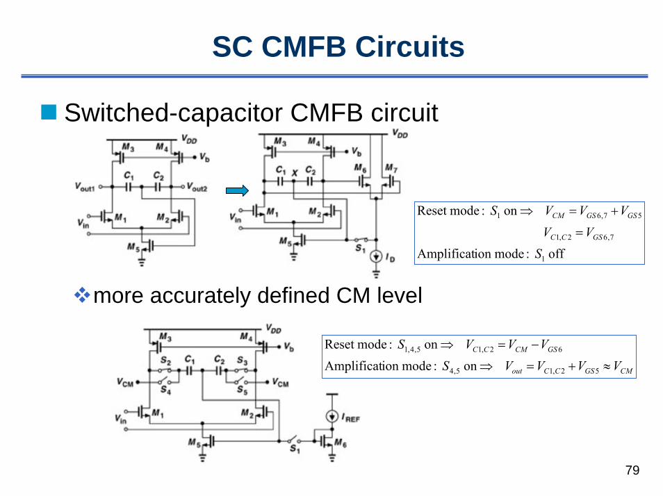
SC CMFB Circuits
Switched-capacitor CMFB circuit
more accurately defined CM level
off :modeion Amplificat
on :modeReset
1
7,62,1
57,61
SVV
VVVS
GSCC
GSGSCM
=
+=⇒
CMGSCCout
GSCMCC
VVVVSVVVS
≈+=⇒
−=⇒
52,15,4
62,15,4,1
on :modeion Amplificat on :modeReset

80
SC CMFB Circuits (cont.)
Another example
)(
)(2)(2))((20)()(
0
))((
))(( :
)()(
)()( :
,12
1,2,
1212
22
22
2
11
11
1
biascmcmoutSC
Scntrl
SC
Ccntrl
biascmScntrlcmoutCcntrlcmoutSC
cntrloutSC
cntrloutSC
biascmScntrloutC
biascmScntrloutC
VVVCC
CVCC
CV
VVCVVCVVCCQQQQ
VVCCQ
VVCCQ
VVCVVCQ
VVCVVCQ
+−+
++
=⇒
−+−=−+⇒
=−+−⇒
=∆+∆⇒
−+=
−+=
−+−=
−+−=
−−++
−+
−−
++
−−
++
φ
φ
)( ,For ,12 cntrlbiascmcmoutcntrlcntrlcntrl VVVVVVV −−===
VCM
φ1φ2
φ1φ2
CS CC
VCM
φ1φ2
φ1φ2
CSCC
Vcntrl
Vbias
VOUT+ VOUT−

81
Two-Stage Opamps
Two-Stage CMOS Opamp with Output Buffer
Equivalent Circuit for Uncompensated Opamp (without Cc and M16)
767
421
// //
dsdsIImmII
dsdsImmI
rrRggrrRgg
====

82
Two-Stage Opamps (cont.)
DC gain:
Frequency Response Without Compensation
Due to the square-law nature, ωp1 and ωp2 are usually quite closed to each other.⇒ Phase margin is significantly less than 45°.⇒ The opamp must be compensated before used in a closed-loop configuration.
)1)(1()(
1' 1'
'2
'1
21
pp
vov
IIIIp
IIp
ssAsA
CRCR
ωω
ωω
++=
==
)(tan)(tan)(
])(1][)(1[|)(|
'2
1'1
1
2'
2
2'1
ppv
pp
vov
jA
AjA
ωω
ωωω
ωω
ωω
ω
−− −−=∠
++=
321
883
2
1
)/(
vvvvo
mLmv
IImIIv
ImIv
AAAAgGgA
RgARgA
××=+≈
−=
−=

83
Compensation
With Compensation Capacitor (Cc)
zero) (RHP
)(
1])1[(
1
z
2
21
C
mII
CICIIIII
CmIIp
CIImIIIICvIp
Cg
CCCCCCCg
CRgRCCAR
=
++≅
≅+−
≅
ω
ω
ω
)(tan)(tan)(tan)(
)1)(1(
)1()(
2
1
1
11
21
ppzv
pp
zvo
v
jA
ss
sAsA
ωω
ωω
ωωω
ωω
ω
−−− −−−=∠
++
−=
Translating the dominant pole toward origin to improve stability
Pole splitting as a result of Miller compensation

84
Compensation (cont.)
Effect of RHP zeroUnity-gain frequency and gain-bandwidth product
'1pω '2pω1pω2pω
product)bandwidth -(gain
1)( )( , Since
frequency.gain -unity Find
11
1
1
1t
CgA
AjAs
AsA
C
mpvot
t
pvotv
p
vovp
==⇒
==⇒≈>>
ωω
ωω
ω
ω
ωω

85
Compensation (cont.)
Effect for the output stage
gmIvd RI
+vd-
gmIIvo1 RII
+vo1-CI
gm8(vo2-vo)
rds8
+vo2-
CII
gm9vo1 rds9
vo
CC
CL
gmIvd RI
+vd-
gmIIvo1 RII
+vo1-CI
CII
CC gm9vo1-gm8vo2vo+
vo2-
RIII CL
o
9 1 8 2
o2
1 2
8
9
8 8
9 9
Find zero by setting v =0.
Using node equation at v , one can obtain1( ) [ ( ) ] 0
1( ) [ ( ) ] 0
1[(1 ) ] 0
m o m o
mII C o C II oII
mmII C C II
m II
m mC II mII z
m m II
g v g v
g sC v s C C vR
gg sC s C Cg R
g gs C C g sg g R
⇒ =
− + + + =
⇒ − + + + =
⇒ − + + + = ⇒ = −
8
9
8
9
1
(1 )
mmII
m II
mC II
m
ggg R
g C Cg
+
− +
zero) (LHP
1,For 98
II
mII
II
IImII
z
mm
Cg
CR
gs
gg
−≈+
−=
=

86
Compensation (cont.)
Lead Compensation (Rz)
Several ways to choose RZ:Taking RZ=1/gmII, one can eliminate the RHP zero.Let ωz=ωp2 to cancel the nondominant pole.However, ωp2 is often not known a priori.Let ωz=1.2ωt to increase the phase margin.
frequency)gain -(unity
)(
1
1
10t
1z
3
C
mIpv
CZg
IZp
CgA
CR
CR
mII
≅≅
−=
=
ωω
ω
ω
)(
1])1[(
1
2
21
CICIIIII
CmIIp
CIImIIIICvIp
CCCCCCCg
CRgRCCAR
++≅
≅+−
≅
ω
ω

87
Compensation (cont.)
Other approaches to Remove RHP zeroEliminating forward signal feedthrough

88
Compensation (cont.)
Indirect Current Feedback
zero) (LHP zC
mcg
Cg
=ω

89
Compensation (cont.)
Indirect feedback compensation without additional power dissipation

90
Design Equations
Slew rate
First-stage gain
Second-stage gain
Gain-bandwidth
First pole
Second pole
Zero (RC=1/gm7)
SRI
CD
C
= 5
)(2
)||(425
14211 λλ +
−=−=
D
mdsdsmV I
grrgA
A g r rg
IV m ds dsm
D
2 7 6 77
7 6 7
2= − =
−+
( || )( )λ λ
ωtm
C
g
C= 1
ωp
V C ds dsA C r r1
2 2 4
1≅
( || )
ωpm m
L
g
C C
g
C27
1 2
7≅+
≅
ωZ → ∞↓(↑)1/2(↑)1/2RHP Zero↑
↑CL↑
↓↑SR ↑
↓(↑)1/2(↑)1/2ωt ↑
↑(↑)1/2↑↑(↑)1/2(↓)1/2(↓)1/2AV ↑
CCL7W7(W/L)6L3,4W3,4L1,2(W/L)1,2ID6ID5
CZg CRmII
)(1
1z −=ω
Positive CMRVcm(max)=VDD-VSD5(sat)-VSG1
Negative CMRVcm(min)=VSS+VGS3+VTp
Positive output swing Vout(max)=VDD-VSD6(sat)-VGS8
Negative output swingVout(min)=VSS+VDS9(sat)
Power dissipationPdiss=(ID5+ ID6+ ID8+ ID10+ ID11)( VDD- VSS)

91
Design Equations (cont.)
Nonlinear Settling Time: due to slew-rate limitingSlew Rate: the maximum rate that output can change
Offset VoltageRandom offset: due to device mismatches resulting from process variations. ⇒employing matching layout techniqueSystematic offset: due to design error
C
D
C
D
C
CcC
out
CI
CI
CI
dtdV
dtdVSR
15(max)
max
2===≅
≡teffttpSG
DLW
OXpmg
C
VVVSR
ICgCt
m
ωω
µω
11
111
)(
,)(2 and Since 1
=+=
==
7
7
3
3
374343
521
)/()/(
mirror.current a toequivalent is M7 and M3. , Since
.2/,For
LWI
LWI
VVVVVVIII
VV
DD
GSGSDSDSGSGS
DDD
inin
=⇒
⇒====
=== −+
5
6
4
7
76
6
6
5
5
)/()/(2
)/()/(
and)/()/(
M6),and(M5mirror current for theAlso
LWLW
LWLW
IILW
ILW
I
DD
DD
=⇒
=
=
occurs. limiting rate-slew no , If
| 0
SlopeSR
Vdt
dVSlope stept
out
>
== = τ

92
Design Equations (cont.)
Alternate Design Equations
])(1][)[(4
)(11
))()(()()(
)(2
)(2
))()(()(
)/2()1(
)/2(1
)(/211
)(1// and
)(1//
)1( . and Let
8712321
8
2882
188
8883
772
12
1121
1111
82
21
89
989988
776
142
521529516
EBpnEBEBpnvvvvo
EBpn
EBLW
oxnpnEBLW
oxn
EBLW
oxnoutmv
EBpnIImv
EBpnEBLW
oxnpn
EBLW
oxnImv
pnEB
DD
pnEBD
DpnEBDdsdsmout
DpndsdsII
DpndsdsI
DDDDDDD
VVVAAAA
V
VCVCVCRgA
VRgA
VVCVCRgA
VPV
VI
IVIgggR
IrrR
IrrR
IVPIIII
λλλλ
λλ
µλλµµ
λλ
λλµλλµ
λλααα
λλ
λλ
λλλλ
αααα
+++=××=
++=
++==
+=−=
+=
+=−=
++++
=++
=
++=
++=
+==
+==
++=⇒==
GBVCISR
PM
gR
Cg
CR
gxg
Cg
CCg
CVVP
CVI
CVC
Cg
EBC
D
p
t
z
t
p
t
mout
L
m
Loutp
mmtz
gs
m
III
mp
CEBDDCEB
D
C
EBLW
oxn
C
mt
15
3
11
2
1
8
83
17
8
772
1211
1
111
tantantan90
)1( 1)1(2.1 2.1
)1(2
)(
==
−
−
−≈
≈≈≈
−=⇒=
≈+
≈
++==
=≈
−−−
ωω
ωω
ωω
ω
ωω
ω
αα
µω

93
Comparison
Comparison

94
Cascode-Cascade Opamp
1
9
29
z
3
99
992
11995753311
11
11
952
32
111995753311
11111199
11
512
175312
1311
1
119
9
575313
1
1
)1(
))1((
11 )1(
1
1)1(
)1(8)()(
)1(2
)()(8
)()(8
12)/2/()/2/(
12//
)1(2)1(
EBCDDC
B
CZEBDD
CZLp
CCZ
m
IZp
EBLDDLEB
B
L
m
CICLLI
Cmp
CDD
EBEBEB
vop
EBCDDCEBC
m
pnEBEBnEBpEBEBEBEBEB
EBEBEBEB
oo
m
moomoo
mvo
DDBDD
VGBCV
PCISR
CRP
VVCRC
CCRg
CR
VCVP
CVI
Cg
CCCCCCCg
CVVVVP
AGB
VCVP
CVI
CgGB
VVVVVVVV
IIVI
VIIVIIVI
ggg
gggggggA
IVIVP
×=+
==
−+
=+
−=−
=
−=
+−=−=−≈
++−≅
+++
−=−=
+===
++=
++=
++=
++=
+=+=
α
αα
ω
ω
ω
αααω
αλλλλλλω
α
λλλλλλλλλλ
λλλλλλ
αα
VDD
VSS
Vin+
M2M1
M3 M4
M5
Vin−
M8
Cc
M6
Cc
M9
Vo+
CL
Vo−
CL
M7 M10
M11 M12M13

95
Low-Voltage Opamp
CMOS Technology

96
Low-Voltage Opamp (cont.)
Input Common-Mode Range of a Differential Input Stage
For Vsat=0.3V, VDD(min)=0.9VVDD=1.5V and Vtn1=0.7V, Vicm(max)=1.9V and Vicm(min)=1.3V
)(51(min)
1)(3(max)
)(5)(1)(3
)(511)(3(min)
satDSGSicm
tnsatSDDDicm
satDSsatDSsatSD
satDSGStnsatSDDD
VVVVVVV
VVV
VVVVV
+=
+−=
++=
++−=

97
Low-Voltage Opamp (cont.)
Parallel NMOS and PMOS Differential Input Stage
Effective input transconductance
1)(5
1)(5
SGPsatSDPDDonp
GSNsatDSNonn
VVVV
VVV
−−=
+=

98
Low-Voltage Opamp (cont.)
Constant gm Differential Input Stage Using Current Compensation
.4 ,For
. ,For
.4 ,0For
)(2
)()(Let
)(2
)(2
bnDDicmonp
bpnonpicmonn
bponnicm
pnmT
POXpNOXn
pPOXpmP
nNOXnmN
IIVVV
IIIVVV
IIVV
IIgL
WCL
WC
IL
WCg
IL
WCg
=<<
==<<
=<<
+=
==
=
=
β
µµβ
µ
µ

99
MOS Switches in Low-Voltage Design
Pass Transistors

100
MOS Switches in Low-Voltage Design (cont.)
Problem for the switch
Use transmission gate.Larger layout areaIt may not turned on for low voltage.
Increase gate voltage to 2.3V.
101
MOS Switches in Low-Voltage Design (cont.)
Charge Pumps (Voltage Generators)

102
MOS Switches in Low-Voltage Design (cont.)
Charge-Pump Clock Driver
Nonoverlapping clock generation circuit

103
MOS Switches in Low-Voltage Design (cont.)
Bootstrap circuit and switching device.
A. M. Abo and P. R. Gary, "A 1.5-V, 10-bit, 14.3-MS/s CMOS Pipeline Analog-to-Digital Converter,” IEEE Journal of Solid-State Circuits, vol 34, May 1999.
104
Switched-Opamp
Design concept
Input structure
Switchable opamp
Switched-capacitor biquad
Switched-opamp biquad
Switched-capacitor integrator
J.Crols and M.Steyaert, “Switched-opamp: An approach to realize full CMOS switched capacitor circuits at very low power supply voltages,” IEEE J. Solid-State Circuits, vol. 29, pp. 936-942, Aug. 1994.

105
Switched-Opamp
Example: Fully-Differential Switched-Opamp MDAC
M. Waltari and K.A.I. Halonen, “1-V 9-bit pipelined switched-opamp ADC” IEEE J. Solid-State Circuits, vol. 36, pp. 129-134, Jan. 2001.

106
Outline
Analog and Mixed-Signal Design in the SOC EraCurrent Mirrors and Biasing CircuitsSingle-Stage AmplifiersOperational AmplifiersLayout of Analog and Mixed-Signal ICs

107
Layout Considerations
Differences Between Layout and CircuitThe differences are mainly due to the following reasons:
These effects are not very substantial for digital systems; but they may have a significant impact on the accuracy of analog circuits and must be avoided or compensated.
Lateral diffusion Etching under the protection
Boundary dependent etchingError in the pattern size due to
Tri-dimensional effects

108
Layout Considerations (cont.)
Absolute and Relative Accuracy

109
Layout Considerations (cont.)
Layout of an analog MOS transistorPoor layout and its equivalent circuit
Correct Layout
Metal profile with multi-contacts and only one contact

110
Layout Considerations (cont.)
Layout of a wide transistorPoor layout
Correct layout (split into several parallel transistors)
⇒ Reducing Csb and Cdb

111
Layout Considerations (cont.)
Layout of Matching TransistorsSources causing transistor mismatches
Gradient effect existing in the fabrication processTo minimize the effect, two transistors that must be matched to each other should be placed very close.For wide transistors, layout techniques to improve matching must be employed.

112
Layout Considerations (cont.)
MOS Matching Model
WLAWLAV VT
t
2
2
2
22
)(
)(
β
ββσ
σ
=∆
=∆

113
Layout Considerations (cont.)
Errors in Matched MOS Transistor Pairs
2
2
222
222
2
2
2
)()/(
1)()(
)()()()(
ββσσσ
σβ
βσσ
∆+∆=∆
∆+∆
=∆
IgVV
VI
gI
I
mtGS
tm
DS
DS
VTm
mt
m
AA
IgV
Ig βσ
ββσ
=⇒∆=∆ )( )()()( 222
2

114
Layout Considerations (cont.)

115
Layout Considerations (cont.)
Layouts of a Differential Pair
Normal layout
Inter-digitized layout Common-centroid layout

116
Layout Considerations (cont.)
Orientation of transistorsPoor layout of transistors with different orientation
Boundary dependent etching Compensation of boundarydependent etching with dummy elements

117
Layout Considerations (cont.)
Layout or Resistors
Layout of two matched resistors
sq)/(resistor sheet :
2
Ω
+=
s
scont
RWLRRRW
L

118
Layout Considerations (cont.)
Resistance is temperature-dependent.Matched resistors should be arranged with their centroids placed
symmetrical with respect to the power devices.
Resistor realized by well diffusion

119
Layout Considerations (cont.)
Layout of Capacitors Cross-section and layout of a capacitor
perimeter. on the depends Matching
)(2)2)(2('
: Undercut)(2
⇒−=
+−×≈−−=
+=×=
×=
xPALWxLW
xLxWA
LWPLWA
At
Cox
oxε

120
Layout Considerations (cont.)
Layout of ratioed capacitors
Capacitors with non-integerMultiple of unit capacitorMatched capacitor with
common-centroid symmetry

121
Layout Considerations (cont.)
Layout of Analog CellsGuidelines
Use transistors with the same orientation.Minimize the source or the drain contact area by stacking transistors.Respect the symmetries that exist in the electrical network as well as in the layout to reduce offset.Use low resistive paths when a current needs to be carried.Shield critical nodes.
Example: two-stage Opamp
Placement of transistors in a stacked fashion

122
Layout Considerations (cont.)
Corresponding layout
Use of dummy transistors in the placement of transistors

123
Layout Considerations (cont.)
Digital Noise CouplingCapacitive couplings
Analog lines routed parallel to the digital lines
Crossing between analog lines and clocks
Separation to reduce horizontal coupling
Dummy line for horizontal shielding
124
Layout Considerations (cont.)
Coupling through the substrateUsing well-shielding
Noise Injection through the power supply
digitalanatot
totanatot
IIIdt
dILIRIRV
+=
++=∆
log
log211
40

125
Layout Considerations (cont.)
Reduce R1: keeping the digital and analog sections as separate as possible and merging them at the place very close to the supply pad.If possible, use separate pads for the analog and digital section.
When extra pins are available, separate pins for the analog and digital supply should be used.Place the supply pins in the middle of the frames.

126
Layout Considerations (cont.)
Floor Planning of Mixed-Signal BlocksGeneral guidelines
Put the analog critical components as far as possible from the digital elements.Make the connections to the critical nodes as short as possible.Avoid crossing between the analog biasing lines and digital busses.
Path of bias and supply lines for basic analog cells
Typical floorplan of an SC filter

127
Layout Considerations (cont.)
Typical floorplan of a fully-differential SC filter
Typical floorplan of a mixed-signal chip

128
Layout Considerations (cont.)
Block Diagram Layout of a Pipelined ADC

129
Layout Considerations (cont.)
Decoupling Capacitors in a Mixed-Signal Chip

130
References
R. J. Baker, CMOS: Circuit Design, Layout, and Simulation, IEEE Press, 2005.P. E. Allen and D. R. Holberg, CMOS Analog Circuit Design, Oxford University Press, Inc., 2002. B. Razavi, Design of Analog CMOS Integrated Circuits, McGraw-Hill, Inc., 2001.D. A. Johns and K. Martin, Analog Integrated Circuit Design, John Wiley & Sons, Inc., 1997. J. E. Franca and Y. Tsividis, eds., Design of Analog-Digital VLSI Circuits for Telecommunications and Signal Processing, Prentice-Hall, 1994.