Embed Size (px)
Citation preview
International Journal of Engineering and Applied Sciences (IJEAS)
ISSN: 2394-3661, Volume-2, Issue-3, March 2015
91 www.ijeas.org
Abstract— Leakage power has become a serious concern in
nanometer CMOS technologies and is a very important issue in
hardware and software design. The leakage power increases as
technology is scaled down. However, with the continuous trend
of technology scaling, it is becoming a main contributor to power
consumption. In the past, the dynamic power has dominated the
total power dissipation of CMOS devices. In advanced
integrated circuits, more power is consumed. In the past many
methods had been proposed for leakage power reduction like
forced stack, sleepy stack, sleepy keeper, dual sleep approach
etc. using techniques like transistor sizing, multi-Vth, dual-Vth,
stacking transistors etc. In this paper, new methods have been
proposed for that. The proposed methods will be compared with
the previous existing leakage reduction techniques. This paper
includes a new technique called dual stack for reducing leakage
and dynamic power and comparison of this technique with old
techniques.
Index Terms— Leakage power, Dual Stack, Sub threshold
Voltage, Tanner EDA 16.2
I. INTRODUCTION
The development of digital integrated circuits is challenged
by higher power consumption. The combination of higher
clock speeds, greater functional integration, and smaller
process geometries has contributed to significant growth in
power density. Scaling improves transistor density and
functionality on a chip. Scaling helps to increase speed and
frequency of operation and hence higher performance. As
voltages scale downward with the geometries, threshold
voltages must also decrease to gain the performance
advantages of the new technology, but leakage current
increases exponentially. Thinner gate oxides have led to an
increase in gate leakage current. Today leakage power has
become an increasingly important issue in processor hardware
and software design. With the main component of leakage, the
sub-threshold current, exponentially increasing with
decreasing device dimensions, leakage commands an ever
increasing share in the processor power consumption. In 65
nm and below technologies, leakage accounts for 30-40For
the most recent CMOS feature sizes (e.g., 90nm and 65nm),
leakage power dissipation has become an overriding concern
for VLSI circuit designers Power consumption of CMOS
consists of dynamic and static components. Dynamic power is
consumed when transistors are switching, and static power is
consumed regardless of transistor switching. Dynamic power
consumption was previously (at 0.18 technology and above)
the single largest concern for low-power chip designers since
dynamic power accounted for 90Technology scaling is one of
the driving forces behind the tremendous improvement in
performance, functionality, and power in integrated circuits
over the past several years. Power dissipation has become a
very critical design metric with miniaturization and the
growing trend towards wireless communication. For
deep-submicron processes, supply voltages and threshold
voltages for MOS transistors are greatly reduced. This to an
extent reduces the dynamic (switching) power dissipation.
However, the subthreshold leakage current increases
exponentially thereby increasing static power dissipation.
Leakage current is the current that flows through a transistor
when it is switched off. It depends on gate length, oxide
thickness and varies exponentially with threshold voltage,
temperature and other parameters. Modern digital circuits
consist of logic gates implemented in the complementary
metal oxide semiconductor (CMOS) technology. Power
consumption has two components: Dynamic Power and
Leakage power. The dynamic power is consumed only when
the circuit performs a function and signals change.
Leakage or static power is consumed all the time, i.e., even
when the circuit is idle. It is unnecessary and one would like to
eliminate it. Scaling and power reduction trends in future
technologies will cause subthreshold leakage currents to
become an increasingly large component of total power
dissipation. Leakage power mainly depends upon
subthreshold leakage current, which increases with the
decrease in threshold voltage. To reduce leakage power,
several techniques have been proposed, including transistor
sizing, multi-Vth, dual-Vth, optimal standby input vector
selection, stacking transistors, dual Vdd, etc. Minimization
power consumption is essential for high performance VLSI
systems. In digital CMOS circuits there are three sources of
power dissipation, the first is due to signal transition, the
second comes from short circuit current which flows directly
from supply to ground terminal and the last is due to leakage
currents. As technology scales down the short circuit power
becomes comparable to dynamic power dissipation.
Furthermore, the leakage power also becomes highly
significant. High leakage current is becoming a significant
contributor to power dissipation of CMOS circuits as
threshold voltage, channel length and gate oxide thickness are
reduced. Consequently, the identification and modeling of
different leakage components is very important for estimation
and reduction of leakage power especially for low-power
applications. Multivariable Threshold voltage CMOS
(MTCMOS) and voltage scaling are two of the methods to
reduce power. Leakage power has been increasing
exponentially with the technology scaling. In advanced
integrated circuits, more power is consumed. Today leakage
Comparative Study of Different Modes for Reducing
Leakage and Dynamic Power through Layout
Implementation
Smt. Sarita Chauhan, Anand Kumar Gupta, Falak Jahan, Rajesh Biyaniya, Surbhi Pathak
Comparative Study of Different Modes for Reducing Leakage and Dynamic Power through Layout Implementation
92 www.ijeas.org
power is an very important issue in hardware and software
design. To reduce this, many methods are implemented like
sleep method, sleepy stack method etc. A sleep transistor is
referred to either a PMOS or NMOS high transistor that
connects permanent power supply to circuit power supply
which is commonly called virtual power supply. The sleep
transistor is controlled by a power management unit to switch
on and off power supply to the circuit. By cutting of the power
source, it reduces the power consumption. The sleep PMOS
transistor is placed between Vdd and pull up network. The
sleep NMOS transistor is placed between ground and pull
down network. Low power has emerged as a principal theme
in todays electronics industry. There are two types of power
consumption-
Static Power- It is also known as leakage power. It is
consumed regardless transistor switching. It depends on
leakage current which decreases with the increase in
subthreshold voltage. Static power is power consumed while
there is no circuit activity.
Dynamic Power- Dynamic power is the power consumed
while the inputs are active. It is consumed only when circuit
performs some operation. It includes short circuit power and
switching power. Switching power is consumed when the
transistors are in active mode. Short circuit power is
consumed when a pull-up and pull-down network are on
turning on and off. Dynamic power dissipation is proportional
to the square of the supply voltage.
II. BACKGROUND
Today leakage power has become an increasingly important
issue in processor hardware and software design. Its reduction
becomes critical in low-power applications such as cell phone
and handheld terminals. Power-gating is the most effective
standby leakage reduction method recently developed. The
development of digital integrated circuits is challenged by
higher power consumption. In this paper, comparison among
different methods for reducing leakage and dynamic power is
done. The dual stack approach shows the least speed power
product among all methods. Therefore, the dual stack
technique provides new ways to designers who require
ultra-low leakage power consumption with much less speed
power product. Leakage power depends on three factors as
threshold voltage, channel length and gate oxide thickness.
Leakage power increases with decrease in these factors.
Furthermore, the structure of the short channel device lowers
the threshold voltage even lower. So it is becoming more and
more important to reduce leakage power as well as dynamic
power.
Previously all the modes are tested through schematic and we
find that layout would give us better result. So that is why our
further work is done through layout implementation and
leakage power is calculated in this paper.
III. TECHNIQUE OF LEAKAGE POWER REDUCTION
Leakage power can be reduced using four different
techniques. Each technique provides an efficient way to
reduce leakage power. They are:
a. Sleep Method
b. Sleepy Stack Method
c. Dual Sleep Method
d. Dual Stack Approach Method
A. Sleep Method
In the sleep approach, a sleep" PMOS transistor is placed
between VDD and the pull-up network of a circuit and a
sleep" NMOS transistor is placed between the pull-down
network and Ground. These sleep transistors turn off the
circuit by cutting off the power rails. The sleep transistors are
turned on when the circuit is active and turned off when the
circuit is idle. By cutting off the power source, this technique
can reduce leakage power effectively. However, output will
be floating after sleep mode, so the technique results in
destruction of state plus a floating output voltage. The circuit
is connected as shown in the figure 1.
Figure 1: Sleep method
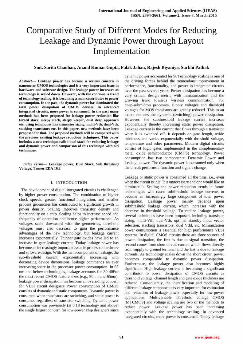
B. Sleepy Stack Method
Another technique for leakage power reduction is the stack
approach, which forces a Stack effect by breaking down an
existing transistor into two half size transistors. The divided
transistors increase delay significantly and could limit the
usefulness of the approach. The sleepy stack approach
combines the sleep and stack approaches. The sleepy stack
technique divides existing transistors into two half size
transistors like the stack approach. Then sleep transistors are
added in parallel to one of the divided transistors. During
sleep mode, sleep transistors are turned off and stacked
transistors suppress leakage current while saving state. Each
sleep transistor, placed in parallel to the one of the stacked
transistors, reduces resistance of the path, so delay is
decreased during active mode. The circuit is connected as
shown in the figure 2.
International Journal of Engineering and Applied Sciences (IJEAS)
ISSN: 2394-3661, Volume-2, Issue-3, March 2015
93 www.ijeas.org
Figure 2: Sleepy stack method
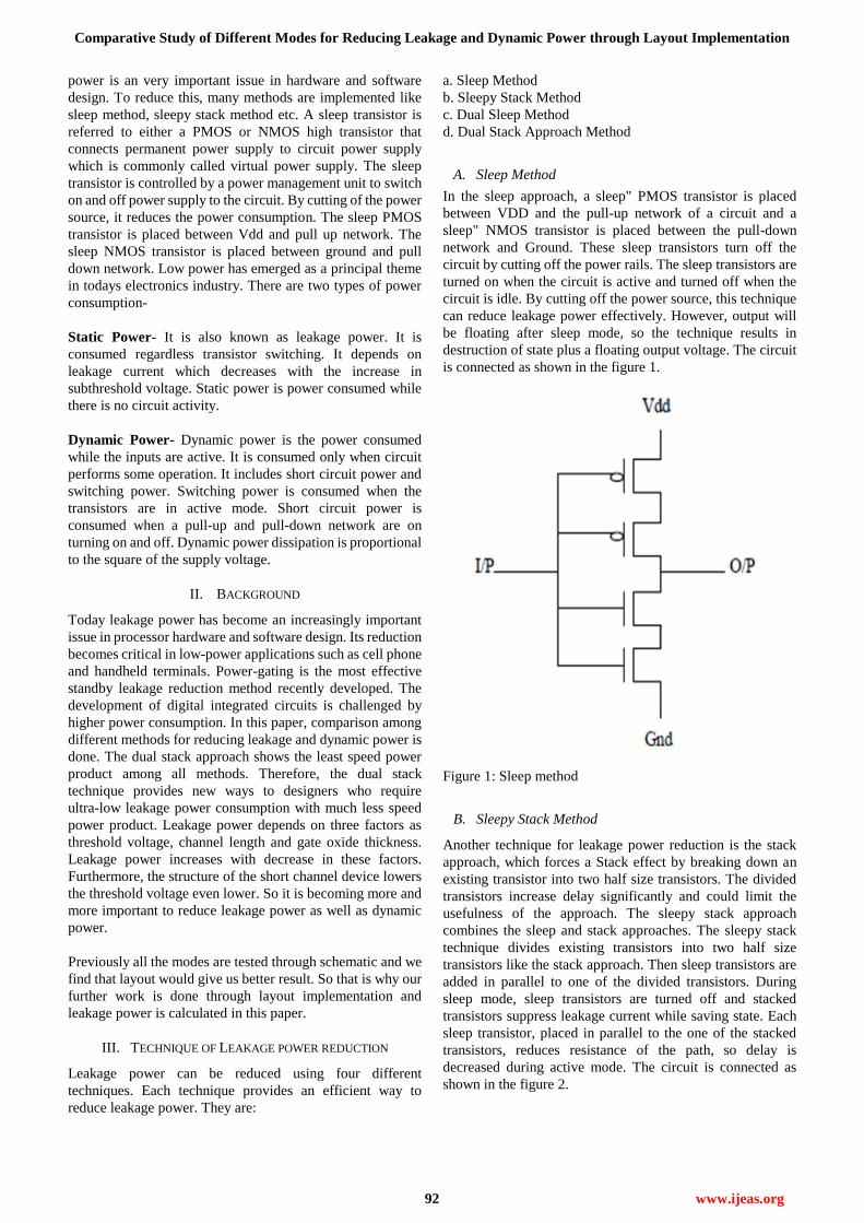
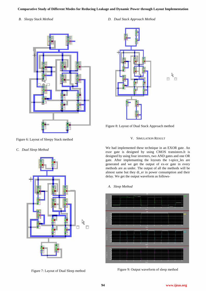
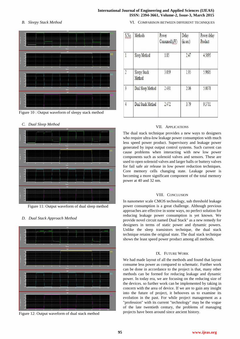
C. Dual Sleep Method
Another technique called Dual sleep approach uses the
advantage of using the two extra pull-up and two extra
pull-down transistors in sleep mode either in OFF state or in
ON state. Since the dual sleep portion can be made common
to all logic circuitry, less number of transistors is needed to
apply a certain logic circuit. The circuit is connected as shown
in the figure below.
Figure 3: Dual Sleep method
D. Dual Stack Approach Method
In this section, the structure and operation of our novel
low-leakage-power design is described. It is also compared
with well-known previous approaches, i.e. the sleepy stack,
dual sleep and sleep transistor method. Here we use 2 PMOS
in the pull-down network and 2 NMOS in the pull up network.
The transistors are held in reverse body bias. As a result their
threshold is high. High threshold voltage causes low leakage
current and hence low leakage power. The circuit is connected
as shown in the figure below.
Figure 4: Dual Stack method
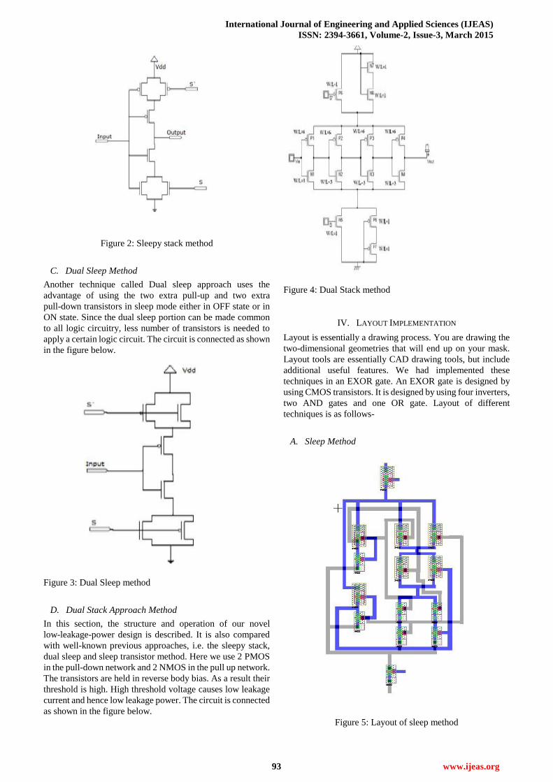
IV. LAYOUT IMPLEMENTATION
Layout is essentially a drawing process. You are drawing the
two-dimensional geometries that will end up on your mask.
Layout tools are essentially CAD drawing tools, but include
additional useful features. We had implemented these
techniques in an EXOR gate. An EXOR gate is designed by
using CMOS transistors. It is designed by using four inverters,
two AND gates and one OR gate. Layout of different
techniques is as follows-
A. Sleep Method
Figure 5: Layout of sleep method
Comparative Study of Different Modes for Reducing Leakage and Dynamic Power through Layout Implementation
94 www.ijeas.org
B. Sleepy Stack Method
Figure 6: Layout of Sleepy Stack method
C. Dual Sleep Method
Figure 7: Layout of Dual Sleep method
D. Dual Stack Approach Method
Figure 8: Layout of Dual Stack Approach method
V. SIMULATION RESULT
We had implemented these technique in an EXOR gate. An
exor gate is designed by using CMOS transistors.It is
designed by using four inverters, two AND gates and one OR
gate. After implemanting the loyouts the t-spice_les are
generated and we get the output of ex-or gate in every
methods are as under. The output of all the methods will be
almost same but they di_er in power consumption and their
delay. We get the output waveform as follows-
A. Sleep Method
Figure 9: Output waveform of sleep method
International Journal of Engineering and Applied Sciences (IJEAS)
ISSN: 2394-3661, Volume-2, Issue-3, March 2015
95 www.ijeas.org
B. Sleepy Stack Method
Figure 10 : Output waveform of sleepy stack method
C. Dual Sleep Method
Figure 11: Output waveform of dual sleep method
D. Dual Stack Approach Method
Figure 12: Output waveform of dual stack method
VI. COMPARISON BETWEEN DIFFERENT TECHNIQUES
VII. APPLICATIONS
The dual stack technique provides a new ways to designers
who require ultra-low leakage power consumption with much
less speed power product. Supervisory and leakage power
generated by input output control systems. Such current can
cause problems when interacting with new low power
components such as solenoid valves and sensors. These are
used to open solenoid valves and larger balls or buttery valves
for fail safe air release in low power reduction techniques.
Core memory cells changing state. Leakage power is
becoming a more significant component of the total memory
power at 40 and 32 nm.
VIII. CONCLUSION
In nanometer scale CMOS technology, sub threshold leakage
power consumption is a great challenge. Although previous
approaches are effective in some ways, no perfect solution for
reducing leakage power consumption is yet known. We
provide novel circuit named Dual Stack" as a new remedy for
designers in terms of static power and dynamic powers.
Unlike the sleep transistors technique, the dual stack
technique retains the original state. The dual stack technique
shows the least speed power product among all methods.
IX. FUTURE WORK
We had made layout of all the methods and found that layout
consume less power as compared to schematic. Further work
can be done in accordance to the project is that, many other
methods can be formed for reducing leakage and dynamic
power. In today era, we are focusing on the reducing size of
the devices. so further work can be implemented by taking in
concern with the area of device. If we are to gain any insight
into the future of project, it behooves us to examine its
evolution in the past. For while project management as a
"profession" with its current "technology" may be the vogue
of the late twentieth century, the problems of managing
projects have been around since ancient history.
Comparative Study of Different Modes for Reducing Leakage and Dynamic Power through Layout Implementation
96 www.ijeas.org
REFERENCES
[1] Ashoka Santhanur, Luca Benini, RowBased Power Gating: A Novel
Sleep Transistor Insertion Methodology for Leakage Power
Optimization in Nanometer CMOS Circuits, IEEE Transactions on
VLSI Systems, Vol. 19, Issue: 3, pp. 469-482, March 2011.
[2] Shuzhe Zhou, Hailong Yao, Qiang Zhou, Minimization of Circuit
Delay and Power through Gate Sizing and Threshold Voltage
Assignment, IEEE Computer Society Annual Symposium on VLSI,
pp. 212-217, 2011.
[3] Philippe Matherat, Mariem Slimani Multiple Threshold Voltage for
Glitch Power Reduction, Faible Tension Faible Consommation
(FTFC), pp. 67-70, IEEE 2011.
[4] Heung Jun Jeon, Yong-Bin Kim, and Minsu Choi, Standby Leakage
Power Reduction Technique for Nanoscale CMOS VLSI Systems,
IEEE Transactions on Instrumentation and Measurement, Vol. 59,
No. 5, pp. 1127-1133, May 2010.
[5] Jae Woong Chun and C. Y. Roger Chen, A Novel Leakage Power
Reduction Technique for CMOS Circuit Design, International
Conference on SoC Design Conference (ISOCC), pp. 119-122 , IEEE
2010.
[6] M. S. Islam, M. Sultana Nasrin, Nuzhat Mansur and Naila Tasneem,
Dual Stack Method: A Novel Approach to Low Leakage and Speed
Power Product VLSI Design, 6th International Conference on
Electrical and Computer Engineering (ICECE), Dhaka, Bangladesh,
pp. 18-20, IEEE December 2010.
[7] M S Islam et al. (2010), Dual Stack Method: A Novel Approach to
Low Leakage and Speed Power Product VLSI Design, Proc.
ICECE2010, 18-20 December, pp. 89-92, Dhaka, Bangladesh.
[8] Pal P K, Rathore R S, Rana A K and Saini G (2010), New low-power
techniques: Leakage Feedback with Stack Sleep Stack with Keeper,
International Conference on Computer and Communication
Technology (ICCCT) pp. 296-301.
[9] Salendra. Govindarajulu, Low Power, Reduced Dynamic Voltage
Swing Domino Logic Circuits Indian Journal of Computer Science
and Engineering, Vol. 1, No. 2, pp. 74-81.
[10] Tezaswi Raja, Vishwani D.Agrawal and Michael L. Bushnell Variable
Input Delay CMOS Logic for Low Power Design, IEEE Transactions
on Very Large Scale Integration (VLSI) System, Vol. 17, Issue: 10,
pp. 1534-1545, 2009.
[11] K. K. Kim and Y.-B. Kim, A novel adaptive design methodology for
minimum leakage power considering PVT variations on nanoscale
VLSI systems, IEEE Trans. Very Large Scale Integration (VLSI), Vol.
17, No. 4, pp. 517528, Apr. 2009.
[12] Sarvesh Bhardwaj and Sarma Vrudhula, Leakage Minimization of
Digital Circuits Using Gate Sizing in the Presence of Process
Variations, IEEE Transactions on Computer-Aided Design of
Integrated Circuits and Systems, Vol. 27, Issue: 3, pp. 445-455,
March 2008.
[13] Se Hun Kim, Vincent J. Mooney III, Sleepy Keeper: a New Approach
to Low-leakage Power VLSI Design, Ix 2006 IFIP International
Conference on Very Large Scale Integration, Oct. 2006, pp.367 372.
[14] S. G. Narendra and A. P. Chandrakasan, Leakage in Nanometer
CMOS Technologies. Berlin, Germany: Springer- Verlag, 2006, pp.
2140.
[15] Salendra. Govindarajulu, Low Power, Reduced Dynamic Voltage
Swing Domino Logic Circuits Indian Journal of Computer Science
and Engineering, Vol. 1, No. 2, pp. 74-81.