Embed Size (px)
Citation preview
sustainablySMART Sustainable Smart Mobile Devices Lifecycles through Advanced Re-design, Reliability, and Re-use and Remanufacturing Technologies
Project Duration: 01/09/2015 - 31/10/2019
Deliverable No.: 4.3
Deliverable title: Device with reused components: Technology demonstration
Type: Demonstrator Version Number: v1 Due Date: 30/09/2019
Actual Submission date: 27/09/2019
Lead Beneficiary: Semicon
Lead Author: Piotr Ciszewski
Deliverable Type: DEM
Dissemination Level: PU
Coordinator contact: Karsten Schischke Fraunhofer IZM phone +49.30.46403-156 e-mail [email protected]
Contributing Partners
SEMICON Sp. z.o.o, Poland
• Piotr Ciszewski • Piotr Dawidowicz • Małgorzata Wierzbicka • Jacek Tomaszewski
INSTYTUT TELE‐ I RADIOTECHNICZNY (ITR), Poland
• Janusz Sitek • Marek Kościelski • Wojciech Stęplewski • Aneta Araźna • Kamil Janeczek • Krzysztof Lipiec • Sebastian Karolewski • Ireneusz Rafalik
SPEECH PROCESSING SOLUTIONS GMBH (Speech), Austria
• Gerhard Podhradsky
TECHNISCHE UNIVERSITAET WIEN (TU WIEN), Austria
• Wolfgang Wimmer • Rainer Pamminger • Sebastian Glaser
Disclaimer
This document reflects only the authors’ view and not those of the European Community. The information in this document is provided “as is” and no guarantee or warranty is given that the information is fit for any particular purpose. The user thereof uses the information at its sole risk and neither the European Commission nor any member of the sustainablySMART consortium is liable for any use that may be made of the information.
This project has received funding from the European Union’s Horizon 2020 research and innovation programme under grant agreement No 680604
sustainablySMART Deliverable No. D4.3 3 | 14
Summary
This report D4.3 is the outcome of WP4, Task 4.1 “Remanufacturing of used semiconductor components: Desoldering” and Task 4.2: “Remanufacturing of used semiconductor components: Re-work” and it demonstrates a feasibility of reusing quality-tested components in new application. The aim of the Deliverable 4.3 is to demonstrate the reuse of remanufactured valuable semiconductor components de-soldered from used mobile products in new devices, which was assembled in industrial environment in Semicon. Based on the conclusions from validation process of elaborated technology verified independently by ITR and Speech partners in lab and industrial environment in the Task 4.2 the components in BGA housing such as flash memory, microcontroller were selected for the new device - the alarm clock device. Based on achieved results and labs tests, the electrical diagram and new device design was created. The new test device was designed to check assembly problems and limitations connected with the second use of remanufactured components in new applications. Based on technique (T3E3) the selected components were remanufactured from the used mobile devices and assembled in industrial environment in new test devices in Semicon. After the reliability tests the final devices were assembled in industrial environment. The lifetime tests carried out, non-destructive (X-ray) and destructive analytics (metallography) tests of the demonstrators verified independently by ITR in lab confirmed high reliability of new devices with remanufactured components.
sustainablySMART Deliverable No. D4.3 4 | 14
Abbreviations AOI Automated Optical Inspection
BGA Ball Grid Array
DVR Digital Voice Recorder
ESD Electrostatic discharge
IMC Intermetallic compounds
MSD Moisture sensitive device
PCB Printed Circuit Board
PCBA Printed Circuit Board Assembly
SMT Surface mount technology
T3E3 Proprietary technology for remanufacturing of BGA components
THT Through-hole technology
WP Work Package
sustainablySMART Deliverable No. D4.3 5 | 14
Content
1 INTRODUCTION ......................................................................................................................... 6
2 THE RELIABILITY OF TEST ASSEMBLIES .......................................................................... 6
3 THE RELIABILITY OF FINAL DEVICE ................................................................................. 10
4 CONCLUSION ............................................................................................................................. 14
5 REFERENCES ............................................................................................................................. 14
sustainablySMART Deliverable No. 4.3 6 | 14
1 Introduction
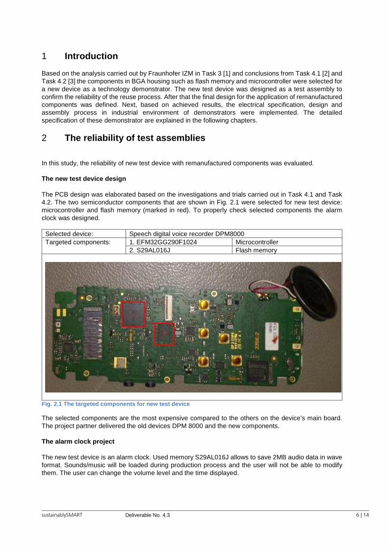
Based on the analysis carried out by Fraunhofer IZM in Task 3 [1] and conclusions from Task 4.1 [2] and Task 4.2 [3] the components in BGA housing such as flash memory and microcontroller were selected for a new device as a technology demonstrator. The new test device was designed as a test assembly to confirm the reliability of the reuse process. After that the final design for the application of remanufactured components was defined. Next, based on achieved results, the electrical specification, design and assembly process in industrial environment of demonstrators were implemented. The detailed specification of these demonstrator are explained in the following chapters.
2 The reliability of test assemblies
In this study, the reliability of new test device with remanufactured components was evaluated. The new test device design The PCB design was elaborated based on the investigations and trials carried out in Task 4.1 and Task 4.2. The two semiconductor components that are shown in Fig. 2.1 were selected for new test device: microcontroller and flash memory (marked in red). To properly check selected components the alarm clock was designed.
Selected device: Speech digital voice recorder DPM8000 Targeted components: 1. EFM32GG290F1024 Microcontroller
2. S29AL016J Flash memory
Fig. 2.1 The targeted components for new test device
The selected components are the most expensive compared to the others on the device’s main board. The project partner delivered the old devices DPM 8000 and the new components. The alarm clock project The new test device is an alarm clock. Used memory S29AL016J allows to save 2MB audio data in wave format. Sounds/music will be loaded during production process and the user will not be able to modify them. The user can change the volume level and the time displayed.
sustainablySMART Deliverable No. 4.3 7 | 14
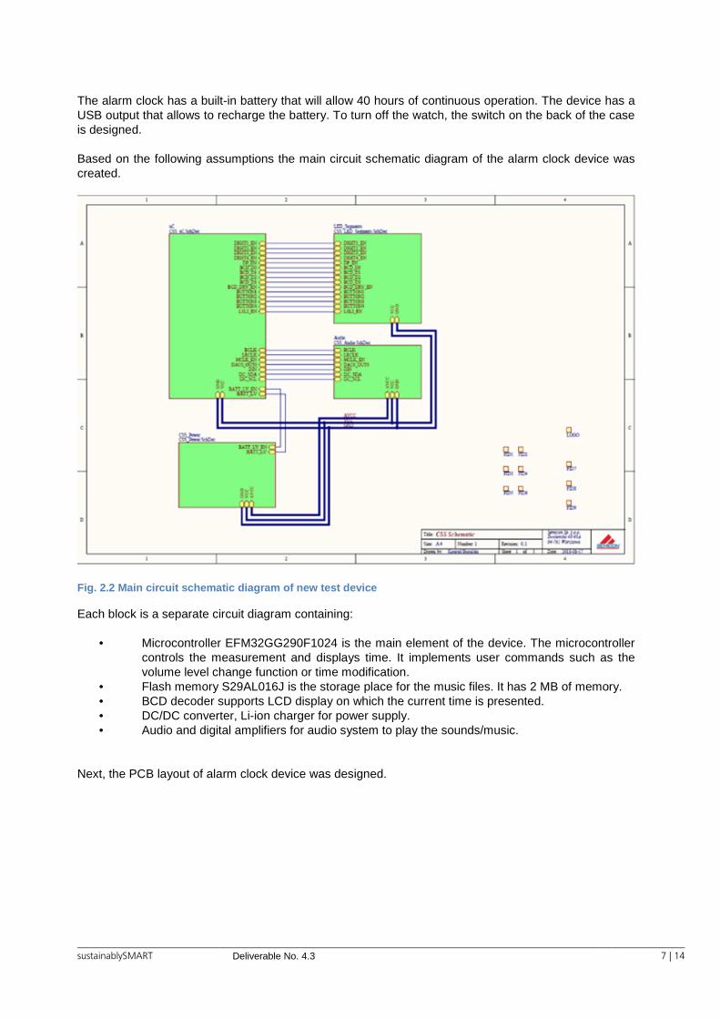
The alarm clock has a built-in battery that will allow 40 hours of continuous operation. The device has a USB output that allows to recharge the battery. To turn off the watch, the switch on the back of the case is designed. Based on the following assumptions the main circuit schematic diagram of the alarm clock device was created.
Fig. 2.2 Main circuit schematic diagram of new test device
Each block is a separate circuit diagram containing:
• Microcontroller EFM32GG290F1024 is the main element of the device. The microcontroller controls the measurement and displays time. It implements user commands such as the volume level change function or time modification.
• Flash memory S29AL016J is the storage place for the music files. It has 2 MB of memory. • BCD decoder supports LCD display on which the current time is presented. • DC/DC converter, Li-ion charger for power supply. • Audio and digital amplifiers for audio system to play the sounds/music.
Next, the PCB layout of alarm clock device was designed.
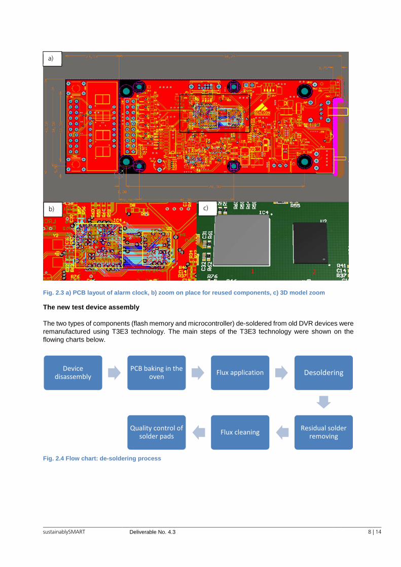
sustainablySMART Deliverable No. 4.3 8 | 14
Fig. 2.3 a) PCB layout of alarm clock, b) zoom on place for reused components, c) 3D model zoom
The new test device assembly The two types of components (flash memory and microcontroller) de-soldered from old DVR devices were remanufactured using T3E3 technology. The main steps of the T3E3 technology were shown on the flowing charts below.
Fig. 2.4 Flow chart: de-soldering process
Device
disassembly
PCB baking in the
ovenFlux application Desoldering
Residual solder
removingFlux cleaning
Quality control of
solder pads
a)
b) c)
sustainablySMART Deliverable No. 4.3 9 | 14
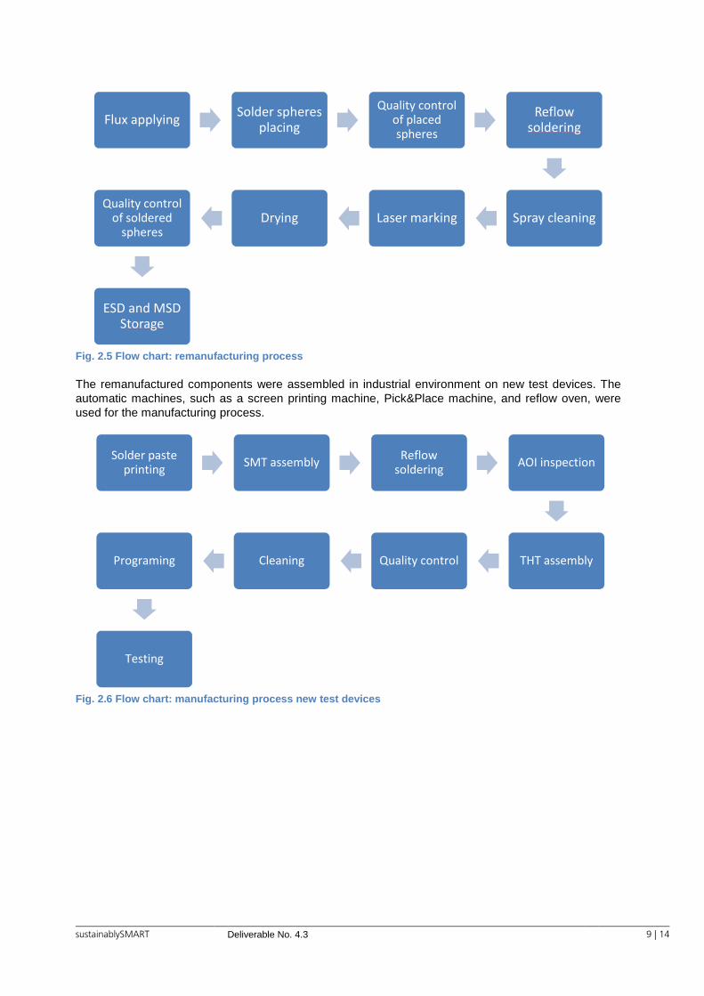
Fig. 2.5 Flow chart: remanufacturing process The remanufactured components were assembled in industrial environment on new test devices. The automatic machines, such as a screen printing machine, Pick&Place machine, and reflow oven, were used for the manufacturing process.
Fig. 2.6 Flow chart: manufacturing process new test devices
Flux applyingSolder spheres
placing
Quality control
of placed
spheres
Reflow
soldering
Spray cleaningLaser markingDryingQuality control
of soldered
spheres
ESD and MSD
Storage
Solder paste
printingSMT assembly
Reflow
solderingAOI inspection
THT assemblyQuality controlCleaningPrograming
Testing
sustainablySMART Deliverable No. 4.3 10 | 14
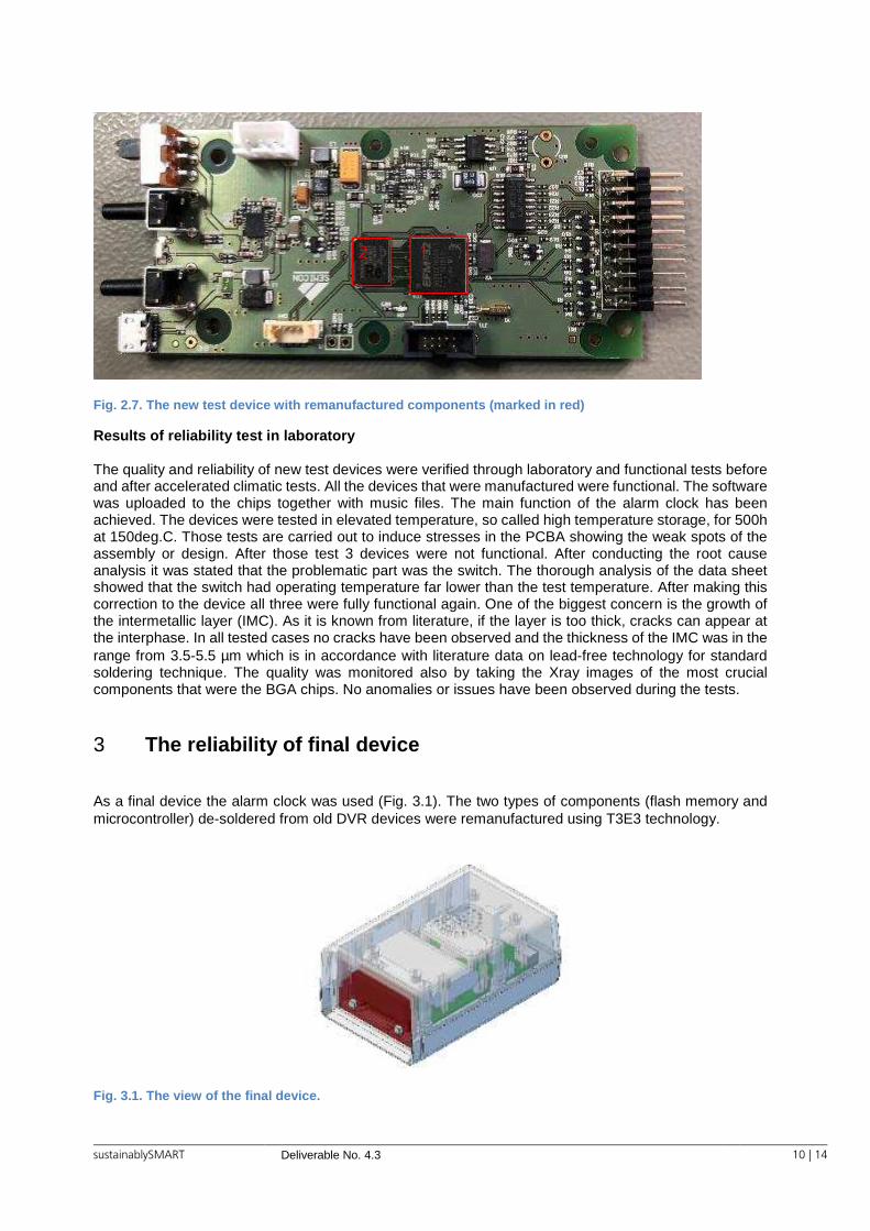
Fig. 2.7. The new test device with remanufactured components (marked in red)
Results of reliability test in laboratory The quality and reliability of new test devices were verified through laboratory and functional tests before and after accelerated climatic tests. All the devices that were manufactured were functional. The software was uploaded to the chips together with music files. The main function of the alarm clock has been achieved. The devices were tested in elevated temperature, so called high temperature storage, for 500h at 150deg.C. Those tests are carried out to induce stresses in the PCBA showing the weak spots of the assembly or design. After those test 3 devices were not functional. After conducting the root cause analysis it was stated that the problematic part was the switch. The thorough analysis of the data sheet showed that the switch had operating temperature far lower than the test temperature. After making this correction to the device all three were fully functional again. One of the biggest concern is the growth of the intermetallic layer (IMC). As it is known from literature, if the layer is too thick, cracks can appear at the interphase. In all tested cases no cracks have been observed and the thickness of the IMC was in the range from 3.5-5.5 µm which is in accordance with literature data on lead-free technology for standard soldering technique. The quality was monitored also by taking the Xray images of the most crucial components that were the BGA chips. No anomalies or issues have been observed during the tests.
3 The reliability of final device
As a final device the alarm clock was used (Fig. 3.1). The two types of components (flash memory and microcontroller) de-soldered from old DVR devices were remanufactured using T3E3 technology.
Fig. 3.1. The view of the final device.
1 2
sustainablySMART Deliverable No. 4.3 11 | 14
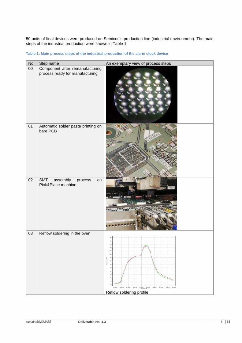
50 units of final devices were produced on Semicon’s production line (industrial environment). The main steps of the industrial production were shown in Table 1. Table 1: Main process steps of the industrial production of the alarm clock device
No Step name An exemplary view of process steps 00 Component after remanufacturing
process ready for manufacturing
01 Automatic solder paste printing on
bare PCB
02 SMT assembly process on
Pick&Place machine
03 Reflow soldering in the oven
Reflow soldering profile
sustainablySMART Deliverable No. 4.3 12 | 14
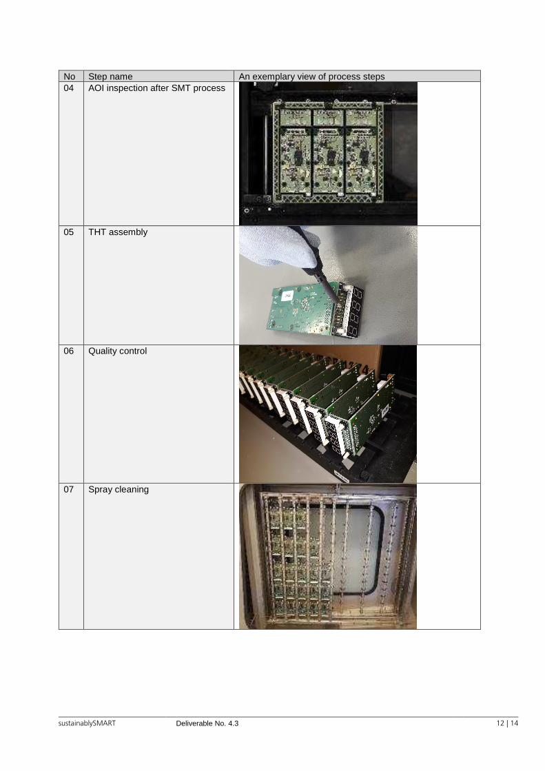
No Step name An exemplary view of process steps 04 AOI inspection after SMT process
05 THT assembly
06 Quality control
07 Spray cleaning
sustainablySMART Deliverable No. 4.3 13 | 14
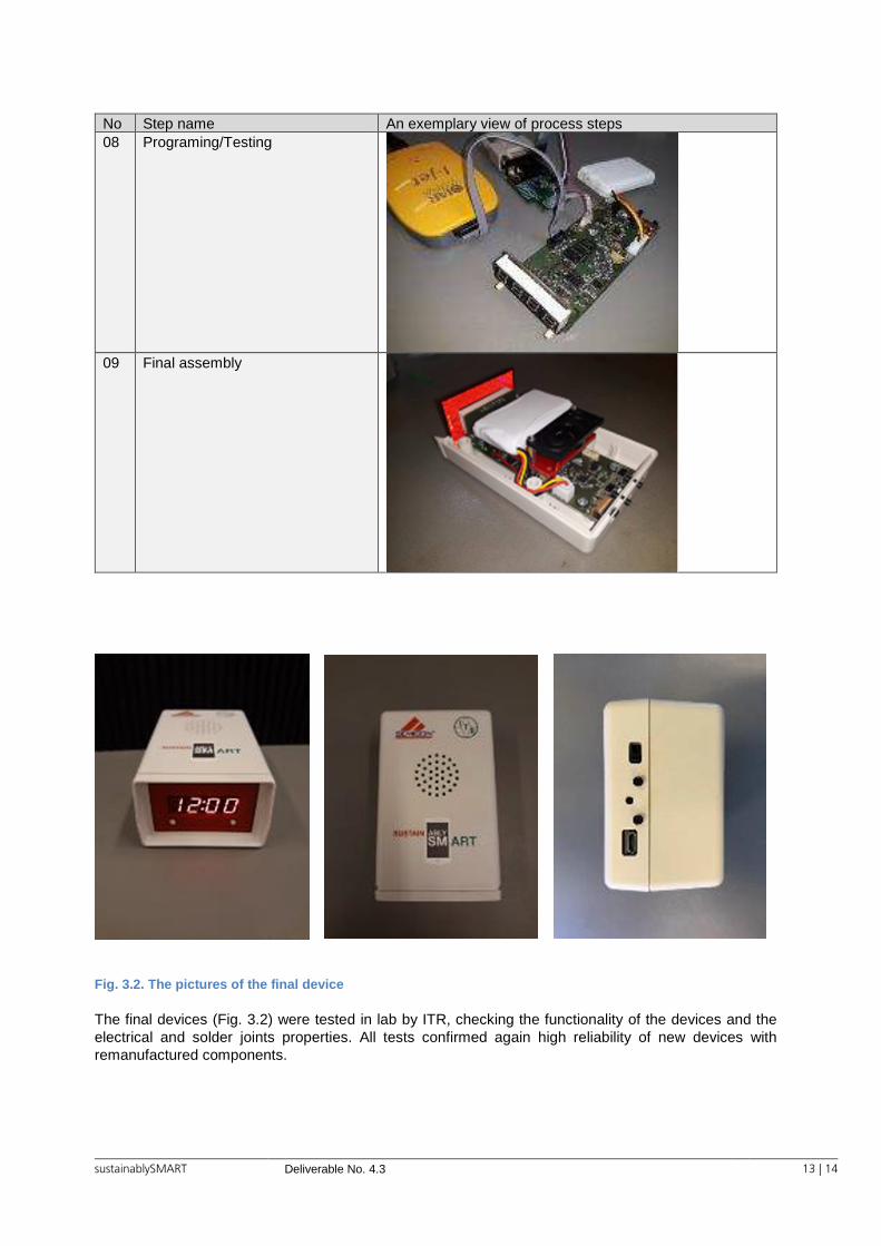
No Step name An exemplary view of process steps 08 Programing/Testing
09 Final assembly
Fig. 3.2. The pictures of the final device The final devices (Fig. 3.2) were tested in lab by ITR, checking the functionality of the devices and the electrical and solder joints properties. All tests confirmed again high reliability of new devices with remanufactured components.
sustainablySMART Deliverable No. 4.3 14 | 14
4 Conclusion
The experiments carried out proved that the use of recovered BGA chips is feasible. Semicon demonstrated the assembly of the boards with industrial equipment. The designed demonstrator devices were functional even after harsh climatic tests. The processes demonstrate implementation of a circular economy approach, advancing the recovery of functional semiconductor packages, thus saving raw materials and replacing potentially newly manufactured semiconductor components.
5 References
[1.] Schischke K. “Milestone No. 2. Definition of target products for sorting and disassembly R&D”, V.01., 07/12/2015
[2.] Tomaszewski, J. “Deliverable No. 4.1. Desoldering process: Technology demonstration”, V.1., 28/02/2017
[3.] Ciszewski, P. “Deliverable No. 4.2. Remanufactured packaged semiconductors: Technology validation”, V.1., 27/04/2018
[4.] Ciszewski, P. “Milestone No. 11. Specification of cascade reuse product(s)”, V.1., 20.08.2018

![Automatic Generation of Explanation for Expert … expert system generic tool (AESGT)[3]. The developed explanation components can be easily reused with expert systems developed by](https://img.pdfslide.tips/doc/110x75/5b2591087f8b9ae13b8b57ad/automatic-generation-of-explanation-for-expert-expert-system-generic-tool-aesgt3.jpg)