Embed Size (px)
Citation preview

EE 236 Electronics
Computer and Systems Engineering Department
Faculty of Engineering Alexandria University
Fall 2017
Bassem Mokhtar, Ph.D. Assistant Professor
Department of Electrical Engineering
Faculty of Engineering
Alexandria University
Introduction 1-1

Outline
Course Overview
Quick Review on Circuit Basics
Introduction to Electronics
Semiconductor Physics
Introduction 1-2

Course Information Instructor: Dr. Bassem Mokhtar
Office hours: TBD
Location: office room 4-4-F132, the 4th EED building floor
Lecture hours: 4 Two Lectures weekly (Sundays and Wednesdays)
Tutorial hours: 1 One tutorial class every two weeks
Lab hours: 1 One experiment every two weeks
Introduction 1-3

Course Website
http://eng.alexu.edu.eg/~bmokhtar/courses/electronics_CSED/fall_2017/electronics_CSED.htm
Introduction 1-4

Course Outline
Introduction to semiconductor physics and materials (1.5 weeks) Conductors vs. Insulators vs. Semiconductors
p-type, n-type
p-n junctions (1.5 weeks) Diodes and diode circuits
BJT transistors (2 weeks) Different types of BJT circuits
DC and AC Biasing
FET transistors (one week) Brief Introduction
MOSFET (2 weeks) Different types of MOSFET circuits
DC and AC biasing
CMOS (2 weeks)
Operational Amplifiers (one week)
Logic and Integrated Circuits (one week) Memory
Introduction 1-5

Course Objectives
Having successfully completed this course, the student will be able to: (a) Comprehensively understand of electronic circuits and devices (diodes, BJTs, MOSFETs)
(b) Learn physical models of the operation of semiconductor devices
(c) Examine the design and operation of important circuits that utilize these devices
Introduction 1-6
Course Prerequisites: Course: EE x11 Electric Circuits
Do you remember? Your last second semester

References
Lecture Notes
“Microelectronic Circuits”, Sedra Smith,5th
edition, 2004.
“Electronic Devices and Circuit Theory”,
Boylestad and Nashelsky, 7th edition
“Fundamentals of Microelectronics”, Razavi,
2006
Introduction 1-7
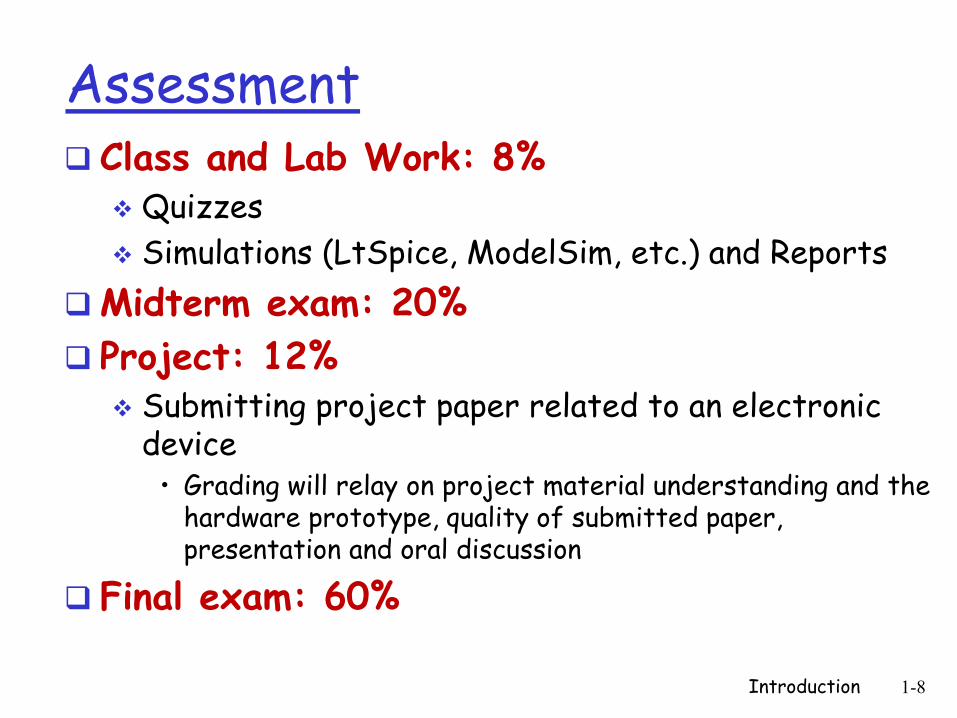
Assessment Class and Lab Work: 8%
Quizzes
Simulations (LtSpice, ModelSim, etc.) and Reports
Midterm exam: 20%
Project: 12% Submitting project paper related to an electronic
device • Grading will relay on project material understanding and the
hardware prototype, quality of submitted paper, presentation and oral discussion
Final exam: 60%
Introduction 1-8

Project
“Smart Electronic Circuit Meter for
Measurement and Analysis” Provide a design for a simple meter that can measure various
parameters at electrical circuits (current, voltage, power, ..) supporting
different loads and give an estimation for any necessary replacement of
elements and learn about the behavior of the connected load (for
example, determining if the load exhibits normal operation or not)
There will be a contest among all groups in the class depending on
The provided design (cost, space complexity, computational load and overhead, features of meter,
capability for development and reconfigurability
Best designs will get bonus marks
Introduction 1-9

Project
The course project will be done in groups of seven (7) students.
The deadline for project groups formation and topics selection is on
Saturday, September 24th, 2017
Each group will work on a specific design and prepare and submit a
project paper
Note, similar designs will get half the project mark as max mark and no bonus (you will
be informed)
Each group should prepare and submit a progress report
Each group should submit a hard copy and an electronic copy of their
final project paper at least two days from the project discussion date
Each group will be given 20 minutes to present their hardware prototype
of the meter in the last week of the semester
Introduction 1-10

Quick Review (Circuit Basics)
Introduction 1-11

Quick Review (Circuit Basics)
Introduction 1-12

Quick Review (Circuit Basics)
Introduction 1-13
Test yourself now:
Write down an equation
for calculating iB in
terms of voltages and
resistors in the circuit

Quick Review (Circuit Basics)
Introduction 1-14

Quick Review (Circuit Basics)
Introduction 1-15

Quick Review (Circuit Basics)
Introduction 1-16

Quick Review (Circuit Basics)
Introduction 1-17

Quick Review (Circuit Basics)
Introduction 1-18

Quick Review (Circuit Basics)
Introduction 1-19

Introduction 1-20
Introduction to Electronics
Block diagram of a simple electronic system: an AM radio.

Introduction 1-21
Introduction to Electronics
Amplifiers
Filters
Signal sources (oscillators)
Wave-shaping circuits
Digital logic functions
Memories
Power supplies
Converters
Common “Blocks” in an Electronic System

Introduction 1-22
Introduction to Electronics
Analog vs. Digital Signals

Introduction 1-23
Introduction to Electronics
Analog to Digital Conversion

Introduction 1-24
Introduction to Electronics
Signals and Noise

Introduction 1-25
Introduction to Electronics
Analog vs. Digital Digital circuits advantages
Better immunity to noise
Easier to implement with IC techniques
More adaptable to variable uses
Analog Circuits advantages
Require less devices
Better to deal with low signal amplitudes
Better to deal with high frequencies

What is the foundation material for all modern electronics ?
Answer: Semiconductor materials
Introduction 1-26

Introduction 1-27

Brief History Rectification in metal-semiconductor contact (Braun, 1874)
Theory of thermionic emission (Bethe 1942)
Transistor (point-contact transistor) using polycrystalline germanium (Shockley, Bardeen and Brattain, 1947)
Bipolar junction transistor (Shockley, 1947)
Integrated circuit (Kilby and Noyce, 1958) using bipolar junction transistors
Practical metal-oxide-semiconductor (MOS) devices (1960s)
Small Scale Integration (SSI) (~10 Trs.chip) ->MSI(~100 Trs/chip)-> LSI (10,000 Trs/chip) in the 1970s)
VLSI (~10^5 Trs/chip) -> ULSI (10^6 Trs/chip) in the 1990s
Multicore chip processors -> 10^8 Trs/core up to 8 processors by 2010
The International Technology Roadmap for Semiconductors (ITRS) predicts 8 nm feature size with 1000 cores in 2020
Introduction 1-28

GOING TO THE FIRST TOPIC
Semiconductor Physics
Introduction 1-29

Introduction 1-30

Semiconductor Materials Atom Bohr Model
Atom have planetary type of structure consisting central nucleus equipped with the proton and surrounded by orbiting electron
Proton are positively charged and electron are negatively charged
Atomic number The atomic number is equal to the number of
protons in an atom’s nucleus
Distinguishes the chemical group characteristics
Electron shells and orbits Electrons near the nucleus have less energy
than the outer one
Electron orbits are grouped in shells (energy bands)
Introduction 1-31
Maximum number of electrons
(Ne) that exist in each shell of
atom can be calculated as
Ne = 2n2
where n(1,2,3,…) is the
number of the shells.
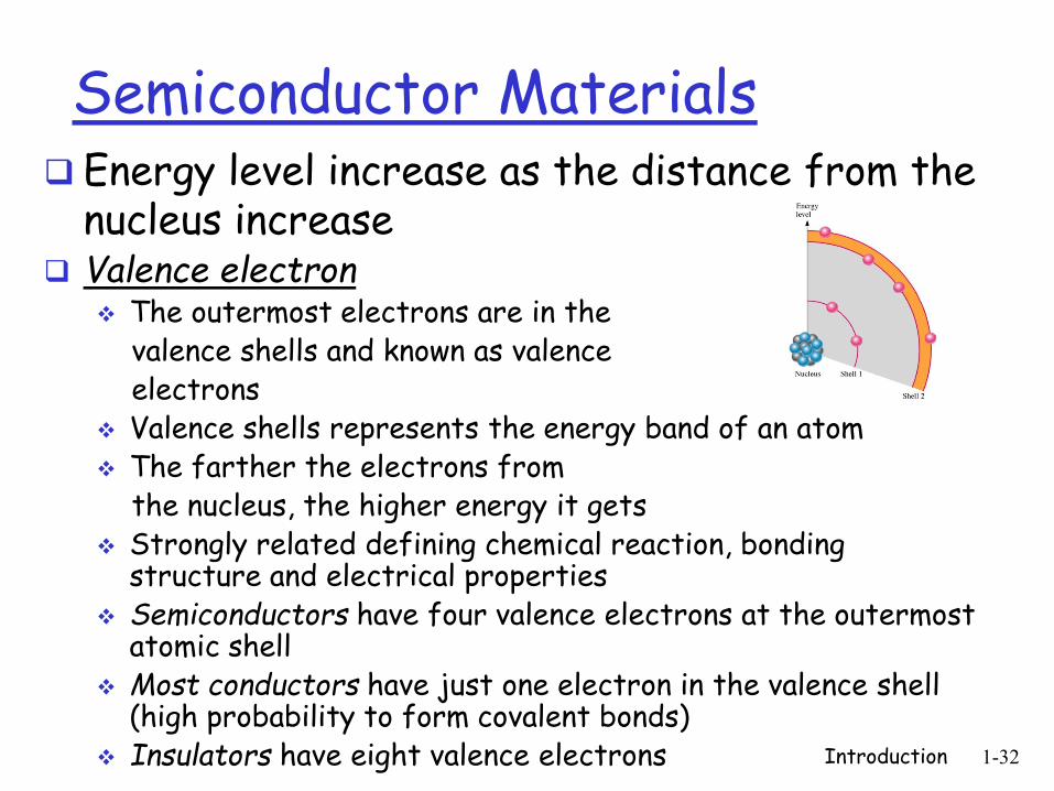
Semiconductor Materials Energy level increase as the distance from the
nucleus increase Valence electron
The outermost electrons are in the valence shells and known as valence electrons Valence shells represents the energy band of an atom The farther the electrons from the nucleus, the higher energy it gets Strongly related defining chemical reaction, bonding
structure and electrical properties Semiconductors have four valence electrons at the outermost
atomic shell Most conductors have just one electron in the valence shell
(high probability to form covalent bonds) Insulators have eight valence electrons
Introduction 1-32

Semiconductor Materials
Introduction 1-33
Valence shells represents the band of energy of an atom
Conduction bands
Existence of free electrons. Where a valence electron becomes a free electron when acquiring enough additional external energy
Energy gaps
Energy differences between conduction bands and valence bands (define the required energy for electron valence to be a free electron)

Comparison Conductor
Easily can conduct electrical current Loosely bounded valence electrons
Insulator Does not conduct electrical current under normal
condition Most insulating materials are compounds Tightly bounded valence electrons
Semiconductor Element that is neither a conductor nor an insulator but
lies between the two elements A material that is between conductors and insulators in
its ability to conduct electrical current Easily affected by temperature and light energy Most of them have 4 valence electrons on the valence
shells-bounded in intermediate strength
Introduction 1-34

Introduction 1-35
Lecture Summary
Covered material Course Introduction
Load, assessment and topics
Quick Review (circuit basics) Introduction to Electronics and Semiconductor
Physics Material to be covered next lecture
Continue Semiconductor Physics Types of semiconductors Types of charge “carriers” in semiconductors Creation of electron-hole pairs Doping