Embed Size (px)
Citation preview

7/27/2019 Exp. 5 Jfet & Mosfet
http://slidepdf.com/reader/full/exp-5-jfet-mosfet 1/5
International University for Science & Technology
College of Engineering and Technology
Electrical Engineering Department
Experiment No.5: JFET & MOSFET
5-1 The Objectives:
1. Introducing JFET.
2. Operating range.
3. Drawing JFET transfer characteristics.
4. Drawing transfer characteristics of the MOSFET.
5. Drawing output characteristics of the MOSFET.
5-2 the Required Equipments:
− Master Board.
− Board Number 70016.
−Computer.
− Transistors: BF 244 & BUZ 73.
5-3 Introduction:
Transistors can be grouped into two major divisions: bipolar and field-effect. In the previous
experiments we studied BJTs, which utilize a small current to control a larger current. In this
experiment, we'll introduce the general concept of the FET - a device utilizing a small voltage to
control current - and then focus on one particular type: the JFET.
All field-effect transistors are unipolar rather than bipolar transistors. That is, the current through
them is comprised either of electrons through an N-type semiconductor or holes through a P-type
semiconductor. This becomes more evident when a physical diagram of the device is seen.
There are tow types of JFET: P-Channel JFET and N-Channel JFET.
Figure 5-1In a JFET, the controlled current passes from source to drain and the controlling voltage is applied
between the gate and source.
With no voltage applied between gate and source, the channel is a wide-open path for electrons to
flow. However, if a voltage is applied between gate and source of such polarity that it reverse-biases

7/27/2019 Exp. 5 Jfet & Mosfet
http://slidepdf.com/reader/full/exp-5-jfet-mosfet 2/5
the PN junction, the flow between source and drain connections becomes limited, or regulated, just as
it was for bipolar transistors with a set amount of base current. Maximum gate-source voltage pinches
off all current through source and drain, thus forcing the JFET into cutoff mode.
This action may be likened to reducing the flow of a liquid through a flexible hose by squeezing it:
with enough force, the hose will be constricted enough to completely block the flow.
Figure 5-2
MOSFET:
Figure 5-3
Placing an insulating layer between the gate and the channel allows for a wider range of control (gate)
voltages. The insulator is typically made of an oxide therefore this type of device is called a Metal-
Oxide-Semiconductor FET (MOSFET) or Insulated-Gate FET (IGFET). The bias voltage on the gateterminal either attracts or repels the majority carriers of the substrate across the PN junction with the
channel. This narrows (depletes) or widens (enhances) the channel, respectively, as V GS changes
polarity.
For N-channel MOSFETs, positive gate voltages (VGS > 0) repel holes from the channel into the
substrate, thereby widening the channel and decreasing channel resistance. Conversely, VGS < 0
causes holes to be attracted from the substrate, narrowing the channel and increasing the channel
resistance. The polarities discussed in this example are reversed for P-channel devices.
The common abbreviation for an N-channel MOSFET is NMOS , and for a P-channel MOSFET,
PMOS .
Since MOSFETs can both deplete the channel and also enhance it, the construction of MOSFET
devices differs based on the channel size in the resting state, VGS = 0. A depletion mode, device (alsocalled a normally on MOSFET) has a channel in resting state that gets smaller as a reverse bias
applied, this device conducts current with no bias applied. An enhancement mode device (also called
a normally off MOSFET) is built without a channel and does not conduct current when VGS = 0;
increasing forward bias forms a channel that conducts current.
Figure 5-4
7/27/2019 Exp. 5 Jfet & Mosfet
http://slidepdf.com/reader/full/exp-5-jfet-mosfet 3/5
5-4 Procedure:
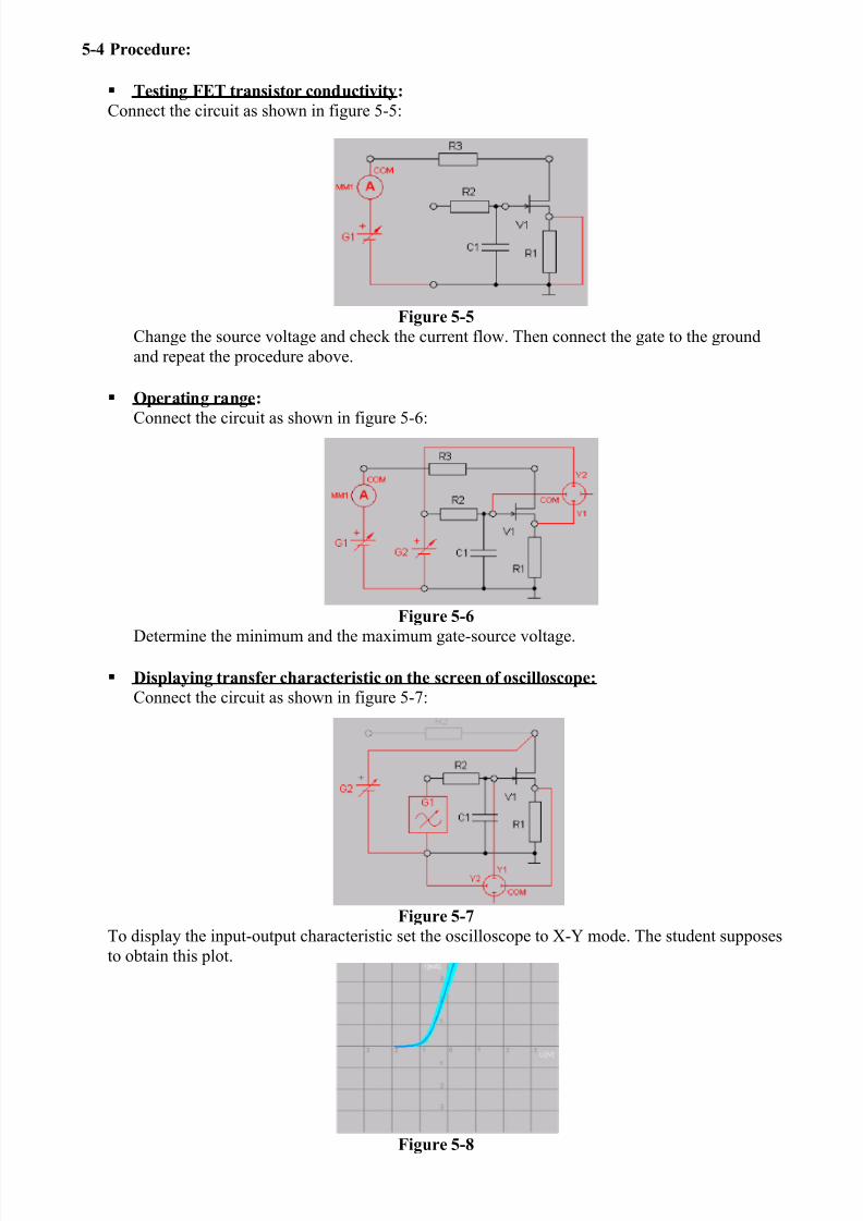
Testing FET transistor conductivity :
Connect the circuit as shown in figure 5-5:
Figure 5-5
Change the source voltage and check the current flow. Then connect the gate to the ground
and repeat the procedure above.
Operating range :
Connect the circuit as shown in figure 5-6:
Figure 5-6
Determine the minimum and the maximum gate-source voltage.
Displaying transfer characteristic on the screen of oscilloscope:
Connect the circuit as shown in figure 5-7:
Figure 5-7
To display the input-output characteristic set the oscilloscope to X-Y mode. The student supposes
to obtain this plot.
Figure 5-8

7/27/2019 Exp. 5 Jfet & Mosfet
http://slidepdf.com/reader/full/exp-5-jfet-mosfet 4/5
Displaying output characteristic on the screen of oscilloscope:
Connect the circuit as shown in figure 5-9.
Figure 5-9
We use the resistor R 3 to calculate the drain current. By varying the drain-source voltage and the
gate-source voltage we can obtain the output characteristic and its relationship to gate-source
voltage. The student supposes to obtain plot similar to this plot.
Figure 5-10
Drawing MOSFET transfer characteristic on the oscilloscope screen :
Connect the circuit as shown in figure 5-11:
Figure 5-11
Set the oscilloscope to X-Y mode in order to plot transfer function which supposes to be similar
to this plot.
Figure 5-12
7/27/2019 Exp. 5 Jfet & Mosfet
http://slidepdf.com/reader/full/exp-5-jfet-mosfet 5/5
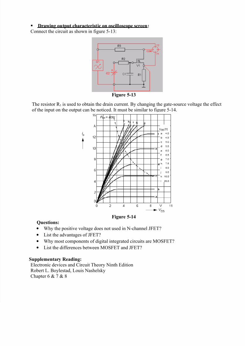
Drawing output characteristic on oscilloscope screen :
Connect the circuit as shown in figure 5-13:
Figure 5-13
The resistor R 3 is used to obtain the drain current. By changing the gate-source voltage the effect
of the input on the output can be noticed. It must be similar to figure 5-14.
Figure 5-14
Questions:
• Why the positive voltage does not used in N-channel JFET?
• List the advantages of JFET?
•Why most components of digital integrated circuits are MOSFET?
• List the differences between MOSFET and JFET?
Supplementary Reading:
Electronic devices and Circuit Theory Ninth Edition
Robert L. Boylestad, Louis Nashelsky
Chapter 6 & 7 & 8