Embed Size (px)
Citation preview
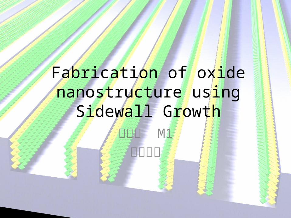
Fabrication of oxide nanostructure using Sidewall
Growth田中研 M1
尾野篤志
VO2LPCMO
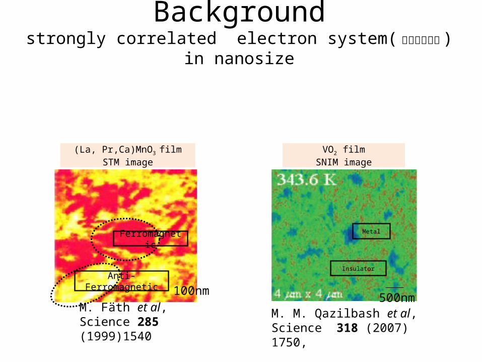
Backgroundstrongly correlated electron system( 強相関電子系 ) in nanosize
100nm100nm 100nm100nm100nmM. Fäth et al, Science 285 (1999)1540
Ferromagnetic
Anti-Ferromagnetic
M. M. Qazilbash et al, Science 318 (2007) 1750,
Metal
Insulator
(La, Pr,Ca)MnO3 filmSTM image
VO2 filmSNIM image
500nm
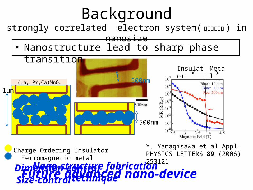
500nm
• Nanostructure lead to sharp phase transition
Backgroundstrongly correlated electron system( 強相関電子系 ) in nanosize
Nano-structure fabrication techniqueSize-control
Insulator Metal
Y. Yanagisawa et al Appl. PHYSICS LETTERS 89 (2006) 253121
500nm
Future advanced nano-deviceDimension-control
(La, Pr,Ca)MnO3 film
Charge Ordering Insulator Ferromagnetic metal
1μm
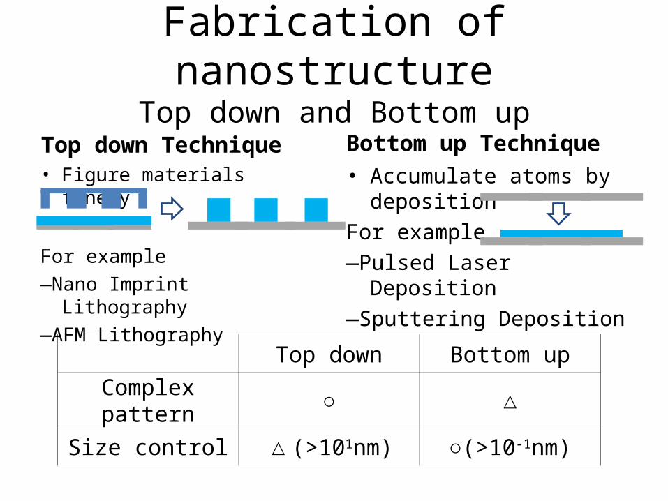
Fabrication of nanostructureTop down and Bottom up
Top down Technique • Figure materials finely
For example―Nano Imprint Lithography―AFM Lithography
Bottom up Technique• Accumulate atoms by
depositionFor example―Pulsed Laser Deposition―Sputtering Deposition
Top down Bottom upComplex pattern
○ △
Size control △ (>101nm) ○(>10-1nm)
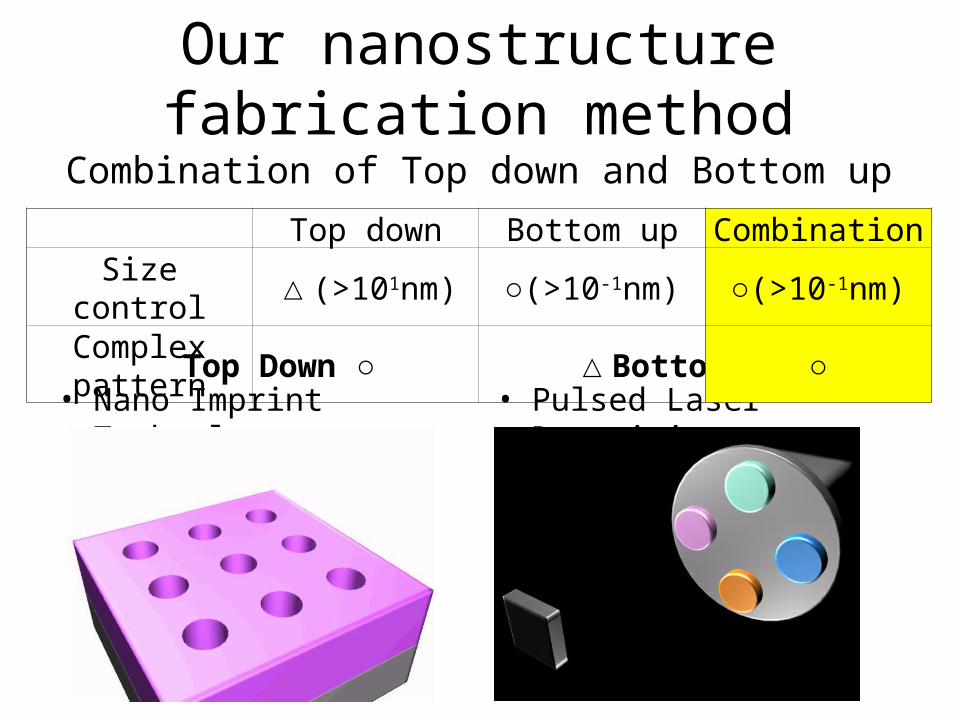
Our nanostructure fabrication methodCombination of Top down and Bottom up
Top Down• Nano Imprint Technology
Bottom up• Pulsed Laser Deposisiton
Top down Bottom up CombinationSize control △(>101nm) ○(>10-1nm) ○(>10-1nm)
Complex pattern
○ △ ○
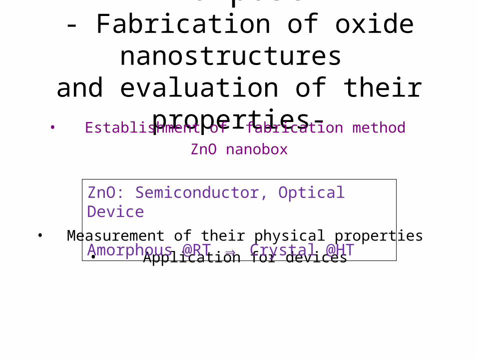
Purpose- Fabrication of oxide nanostructures
and evaluation of their properties-• Establishment of fabrication method
ZnO nanobox
• Measurement of their physical properties• Application for devices
ZnO: Semiconductor, Optical Device
Amorphous @RT ⇒ Crystal @HT
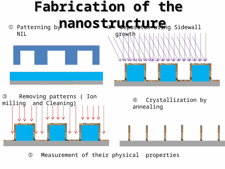
Fabrication of the nanostructureFabrication of the nanostructure① Patterning by NIL ② Depositon using Sidewall growth
③ Removing patterns ( Ion milling and Cleaning) ④ Crystallization by annealing
⑤ Measurement of their physical properties
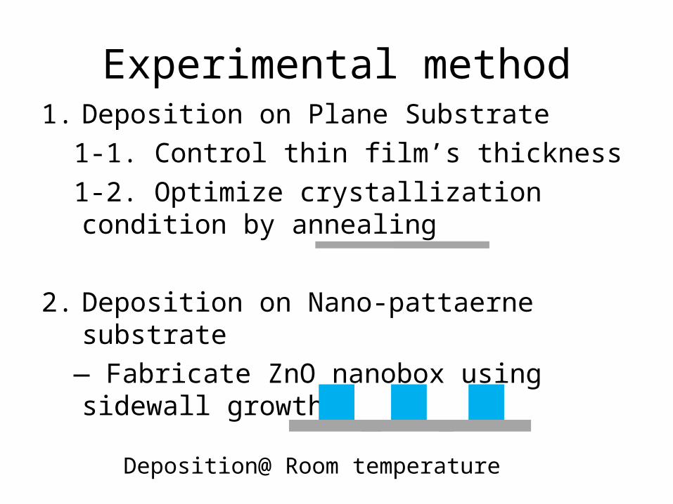
Experimental method1. Deposition on Plane Substrate 1-1. Control thin film’s thickness 1-2. Optimize crystallization condition by
annealing
2. Deposition on Nano-pattaerne substrate ― Fabricate ZnO nanobox using sidewall
growth
Deposition@ Room temperature
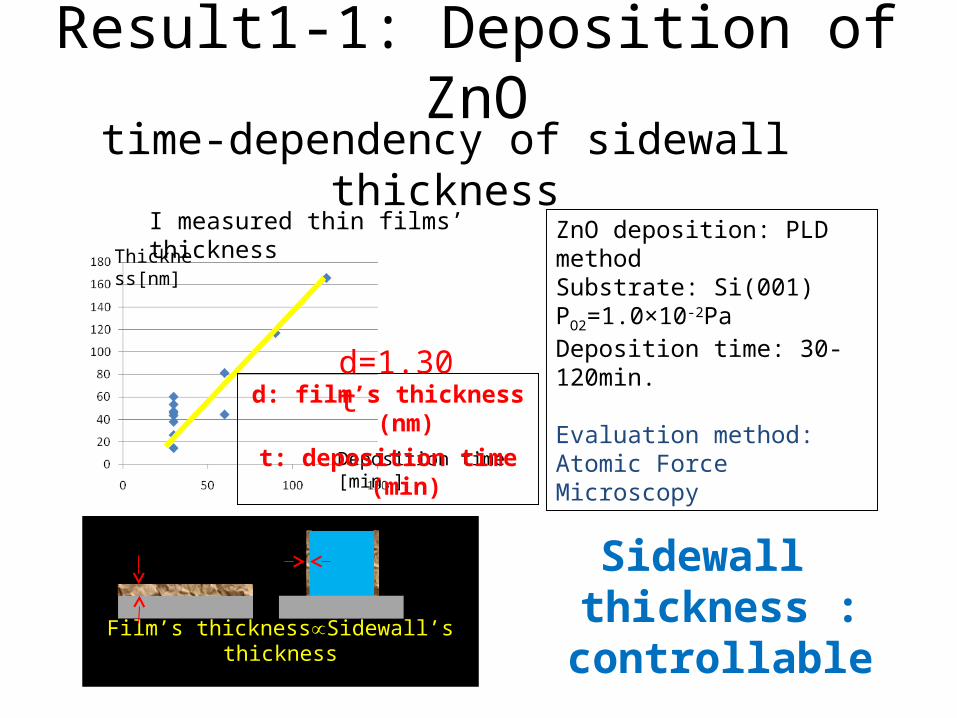
Result1-1: Deposition of ZnO
time-dependency of sidewall thickness
Deposition time [min.]
Film’s thickness∝ Sidewall’s thickness
I measured thin films’ thickness
Sidewall thickness : controllable
Thickness[nm]
ZnO deposition: PLD methodSubstrate: Si(001)PO2=1.0×10⁻²PaDeposition time: 30-120min.
Evaluation method:Atomic Force Microscopyd: film’s thickness (nm)
t: deposition time (min)
d=1.30t
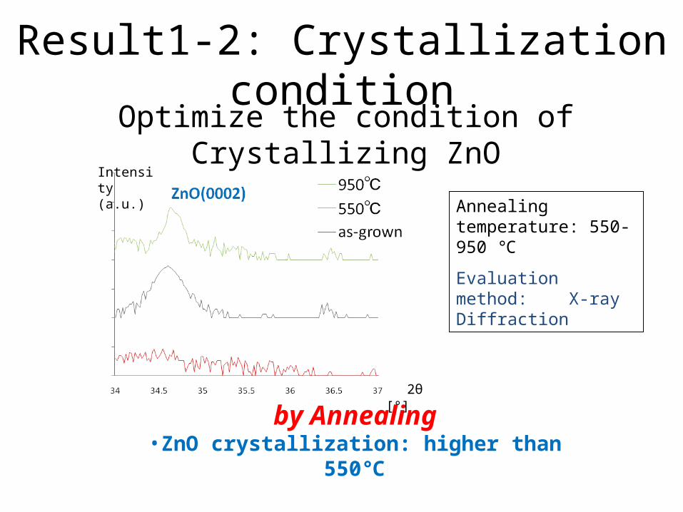
Result1-2: Crystallization condition
Optimize the condition of Crystallizing ZnO
by Annealing•ZnO crystallization: higher than 550℃
Annealing temperature: 550-950 ℃
Evaluation method: X-ray Diffraction
2θ [°]
Intensity (a.u.)
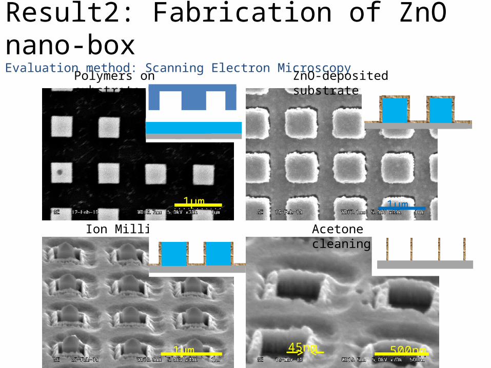
1μm 1μm
1μm 500nm45nm
Polymers on substrate
Ion Milling
Result2: Fabrication of ZnO nano-boxEvaluation method: Scanning Electron Microscopy
ZnO-deposited substrate
Acetone cleaning
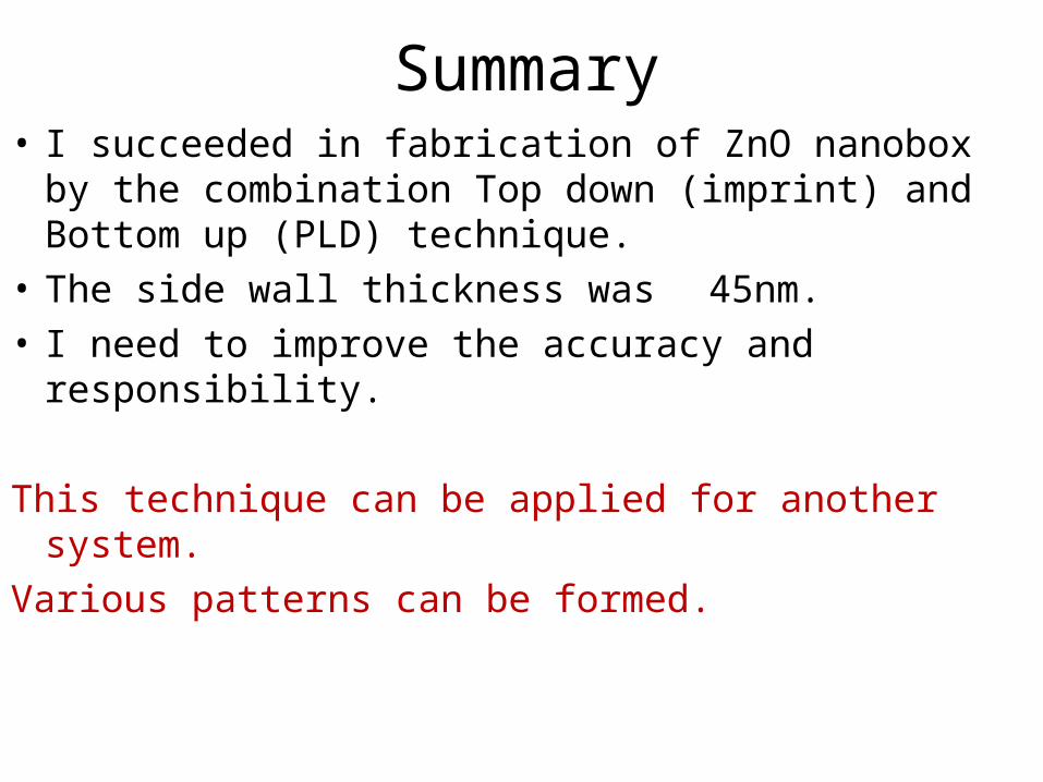
Summary• I succeeded in fabrication of ZnO nanobox by the
combination Top down (imprint) and Bottom up (PLD) technique.
• The side wall thickness was 45nm.• I need to improve the accuracy and responsibility.
This technique can be applied for another system.Various patterns can be formed.
2 µm
100 nm
200 nm
200 nm
60nm
150 nm
150 nm
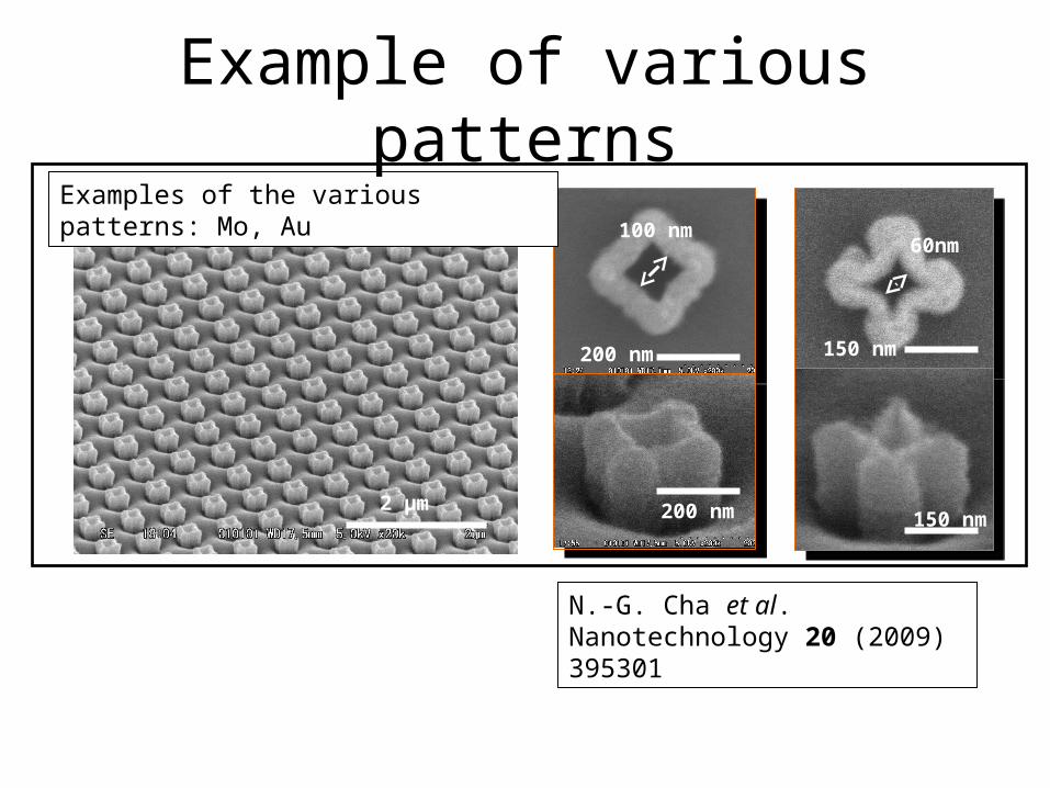
Examples of the various patterns: Mo, Au
Example of various patterns
N.-G. Cha et al. Nanotechnology 20 (2009) 395301
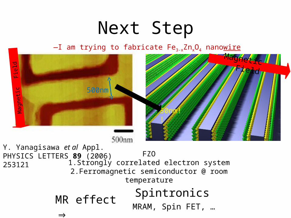
Next Step―I am trying to fabricate Fe3-xZnxO4 nanowire
500nm
50nm!!
MR effect ⇒MRAM, Spin FET, …
Spintronics
Y. Yanagisawa et al Appl. PHYSICS LETTERS 89 (2006) 253121 FZO
1.Strongly correlated electron system2.Ferromagnetic semiconductor @ room temperature
Mag
netic
F
ield
Magnetic Field