Embed Size (px)
Citation preview

How to use the design tool (Ver 1.0) for FAN7631
www.fairchildsemi.com
1

Contents
Motivations Design Example
Single output for LCD TV
2

Motivations
It is modified from conventional Fairchild LLC design tool of version 1.3
It is suitable for FAN7631 in the control parameter design point of view
It can be used for high frequency design with resonant frequency up to 300kHz and softstart frequency up to 600kHz
3

Design ExampleDesign ExampleSingle Output Application for LCD TV
4

Design Example
Single output application for LCD TV Specifications p
Output: 24V/8A Input: 360Vdc ~ 400Vdc (nominal 380Vdc)
L t’ t t t d i i “LLC d i t l f FAN7631 V 1 0” Let’s start to design using “LLC design tool for FAN7631 Ver 1.0
5

Step 1: Fill out the input/output specifications
Multi-output could be possible up to three.
Specification & Parameter Input Dim. Output Dim.
1 O t t S ifi ti
Output Voltage 1 24 VOutput Current 1 8 AOutput Voltage 2 0 VOutput Current 2 0 AO t t V lt 3 0 V1. Output Specifications Output Voltage 3 0 VOutput Current 3 0 AOutput Power 192.0 WSelect Configuration of Output Rectifier 1Maximum VF of Output Diode 1 VMaximum Input Voltage 400 V
2. Input Specifications
Maximum Input Voltage 400 VNominal Input Voltage 380 VEstimated Efficiency 0.95Expected Input Power 202.1 WDC-Link Capacitor 680 uFFrequency & Ripple voltage @ Nominal 0 Hz 0 V
If this is larger than the gap between Vin,nom and Vin,mim, increase the DC-Link Capacitor.
Minimum Input Voltage 360 V
If the secondary side configuration is a center tapped, input “1”. If the secondary side configuration is a bridge type, input “2”.
If the PFC circuit is used, then these two rows have no meaning
6
no meaning.

Step 2-1: Select m (Lp/Lr)
It is recommended to choose 4~8 of m. The conduction loss would be decreased as m increases.
3 G i & T ti
m= 6Boundary Voltage 411 VGain @ Resonant Freq. of Lr & Cr 1.10 Margin of Maximum Gain 15 %
3. Gain & Turn ratiog
Required Maximum Gain 1.44 Turn-ratio (Np/Ns1) 9.00 Turn-ratio (Np/Ns2) -Turn-ratio (Np/Ns3) -
Gain
1. To make all switching frequencies depending on the input voltage below the resonant frequency (fs<fo), let the Boundary Voltagehigher than the maximum input voltage.
Below region(fs<fo)
Above region(fs>fo)
Gain
higher than the maximum input voltage.If Boundary Voltage is less than Vin,max, above region operation could be with Vin,max.
2. To make turns ratio be an integer, tune the Boundary Voltage up.
Gmax @ Vin,min
Gmin @ Vin,max
Virtual Gain@ Boundary Voltage
7
fs@ Vin,min
fs@ Vin,max
fo
fs

Step 2-2: Select m (Lp/Lr)
m= 6Boundary Voltage 411 VGain @ Resonant Freq. of Lr & Cr 1.10
3. Gain & Turn ratioMargin of Maximum Gain 15 %Required Maximum Gain 1.44 Turn-ratio (Np/Ns1) 9.00 Turn-ratio (Np/Ns2) -Turn-ratio (Np/Ns3) -
IpIm
(I) fs < fo To respond properly to load changes, there should be an enough margin. 15~20% is
d d
IOID
recommended.
(II) f > fThe peak gain in the gain curve must exceed
Ip
ID IO
Im
(II) fs > fop g g
the Required Maximum Gain at full load condition.
8

Step 3-1: Select Q factor
This graph is obtained when m is selected. Find out an appropriate Q factor guaranteeing the
GRequired Maximum Gain on the red curve.
In previous page:p p g1) m is selected to be m=6 2) required peak gain is calculated to be 1.44
Action items:1) find the curve with m=6 which is highlighted
with redwith red 2) @ m=6 curve, find a pint of gain=1.443) read the Q value @ the point of gain=1.44
and find the Q is around 0.35
9

Step 3-2: Select Q factor
Automatically calculated.
4. Resonant Parameters
AC Resistor 214.2 ohmDC Resistor 3.3 ohmQ factor 0.350Expected Resonant Frequency 200 kHzRecommended Cr 10.6 nFRecommended Lr 59.7 uHSelected Cr / Recomm. Voltage Rating 12.0 nF 630 VSelected Lr 60.0 uH
Estimated Lp 360.0 uH
To guarantee the Required Maximum Gain, Q factor has to be small satisfactorily.
Put the desired resonant frequency down.
Lr and Cr could be calculated using;
rrO CL
f2
1
AC
r
r
RCL
Q
Put the desired resonant frequency down.
Choose Lr and Cr referring to the Recommended Values including the voltage rating of Cr.
10
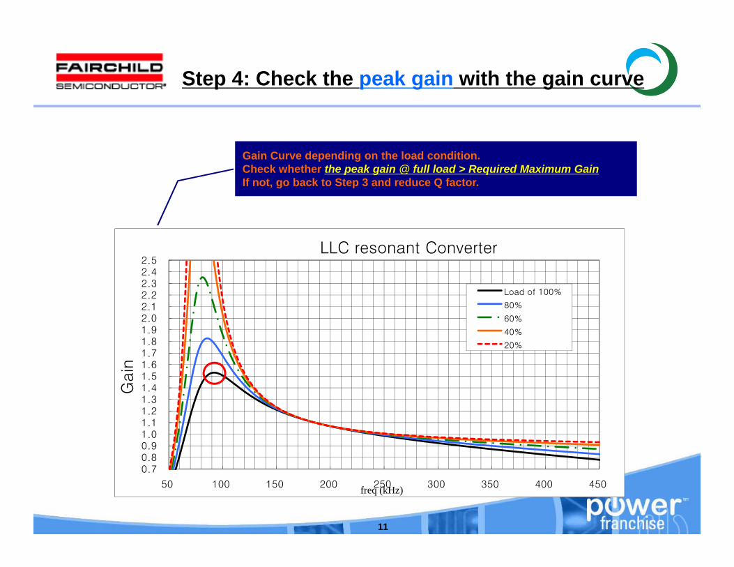
Step 4: Check the peak gain with the gain curve
Gain Curve depending on the load condition. Check whether the peak gain @ full load > Required Maximum Gain
LLC resonant Converter
If not, go back to Step 3 and reduce Q factor.
2 02.1 2.2 2.3 2.4 2.5
LLC resonant Converter
Load of 100%
80%
60%
1.41.5 1.6 1.7 1.8 1.9 2.0
Gain
60%
40%
20%
0.8 0.9 1.0 1.1 1.2 1.3 1.4 G
0.7
50 100 150 200 250 300 350 400 450 freq (kHz)
11

Step 5: Just check out Section 5 and 6
Section 5 is only for the reference.Remind Lp and Lr are not Lm and Llkg.
5. Transformer Parametersfor Simulation
Magnetizing Inductance 328.6 uHLeakage Inductance of Primary-side 31.37 uHInductance of Secondary-side 1 4.05 uHLeakage Inductance of Secondary-side 1 0.39 uHInductance of Secondary-side 2 - uHyLeakage Inductance of Secondary-side 2 - uHInductance of Secondary-side 3 - uHLeakage Inductance of Secondary-side 3 - uHPhase Angle of Lr & Cr 1178.5 krad/sPhase Angle of Lp & Cr 481.1 krad/s
6. Operating ParametersResonant Freq. of Lr & Cr (fr) 187.7 kHzResonant Freq. of Lp & Cr 76.6 kHzOperating Freq. @ Max. Input Voltage 175.8 kHzOperating Freq. @ Nom. Input Voltage 159.4 kHzOperation Freq. @ Min. Input Voltage 141.9 kHz
The real value of resonant frequency.
Estimated operating frequencydepending on the input voltage.Check out all are below resonant frequency.
12

Step 6: Obtain components’ values of control part
Mi i O i F f IC 75 kH
Referring to the gain curve, put down the minimum operating frequency.Keep it in your mind that the set must do not enter the ZCS mode.
It is set for burst Minimum Operating Frequency of IC 75 kHzMaximum Operating Frequency of IC 200 kHzfss 450.0 kHzRmin 7.7 kohmRmax 4.2 kohmSoft-start Time(tSS) 30.00 msec
operation
It is 6fmin and upper limit is 600kHz
7. Parameter ofControl Part
Css 0.35 uFAuto Restart Time(tAR) 243 msOLP Time(tOLP) 40 msRecommended Sensing Resistor(RCS) 0.13 ohmInput Voltage for disabling Brownout Protection 380 VInput Voltage for enabling Brownout Protection 360 00 V
Css related section(tSS, tAR, TOLP)
Input Voltage for enabling Brownout Protection 360.00 VVin, hysteresis 20.00 VRupper_LUVP 2.00 MΩRlower_LUVP 16.8 kΩDead Time(DT) 280 nsDead Time Resistor(RDT) 9.9 kΩ
Dead Time Capacitor (CDT) 10.0 nF
Brownout protection section
To avoid triggering of OCP at startup, there is 50% margin of the estimated
Dead time section
13
peak primary current.

Step 7: Just check out Section 8
The estimated rms value of the primary current. The more m, the smaller Irms.If the transformer is too hot, there are two solutions;
First, go back to Step 2 and increase m.Second, increase wire gauge as large as possible.
8. Current on Input & Output Stage
IRMS of Primary-side @ Nominal Input 1.16 Arms
IPEAK of Primary-side @ Nominal Input 1.64 A
IRMS of Output 1 9.59 Arms
IRMS of Output 2 - Arms
IRMS of Output 3 - Arms
It will be used to select the sense resistor.To avoid triggering of OCP at startup, there is 50% margin of the estimated peak primary current.
14

Step 8: Select the secondary diode
9. Secondary-Side
Margin of Rated Voltage 50 %Margin of Rated Current 100 %
Rated Current & Voltage of Output 1 Diode72.0 V8.60 A
Diode SpecificationRated Current & Voltage of Output 2 Diode
- V- A
Rated Current & Voltage of Output 3 Diode- V
- A
The voltage rating is (2*Vo)*150% as your input. The current rating has 100% margin.
15

Step 9: Transformer Design
To guarantee safe operation, recommended BMAX when integrated transformer1) 0.2~0.26 for fr=100kHz2) 0.15~0.2 for fr=200kHz3) 0.1~0.15 for fr=300kHzis recommended.
Expected BMAX 0.2 Tesla
Ae of Core 150
Min. Number of Primary Winding Turns(Np,min) 25.0 TurnsNumber of Output 1 Winding Turns(Ns1) 3 02 Turns
Used core information
Minimum Np. Np must be greater than this.
10. Transformer Specifications
Number of Output 1 Winding Turns(Ns1) 3.02 TurnsNumber of Expected Primary Winding Turns(Np) 27.2 TurnsNumber of Output 2 Winding Turns(Ns2) - TurnsNumber of Output 3 Winding Turns - TurnsPrimary-side Inductance (Lp) 360.0 uHResonant Inductance (Lr) 60.0 uHCurrent Density 5 A/Area of Primary Winding Wire 0.23
Area of Output 1 Winding Wire 1.25
Area of Output 2 Winding Wire -
Area of Output 3 Winding Wire -
Select the current density and the adequate wire. If the window area of the used core is insufficient with the recommended winding wire, increase the current density.
Among multi-outputs, fill in the blank with the lowest output.If Np<Np,min, error message is like below, so please increase Ns1
16

Considerations
4~8 of m is recommended. Let Boundary Voltage above Vin,max. Select Q factor for “Peak Gain > Required Maximum Gain.” Set fs,min to avoid ZCS region operation. Set the voltage margin for selecting the secondary diodeSet the voltage margin for selecting the secondary diode. Np must be greater than Minimum Np. If the temperature of transformer is too high,
G b k t St 2 d iGo back to Step 2, and increase m. Go back to Step 9, and decrease Current Density.
17

Thank you !
18