Embed Size (px)
Citation preview

IEEE P
roof
IEEE JOURNAL OF SELECTED TOPICS IN QUANTUM ELECTRONICS 1
ZnO Nanorod-Based Ultraviolet PhotodetectorPrepared on Patterned Sapphire Substrates
1
2
Fang-Hsing Wang, Member, IEEE, and Chih-En Tsai3
Abstract—A patterned sapphire substrate with a submicron holeQ1
4array structure was used to fabricate ZnO nanorod (NR) array5by low-temperature hydrothermal method. A ZnO seed layer was6spin-coated using sol-gel process and then etched to form sep-7arated seed islands. Different concentrations of zinc acetate in8the hydrothermal solution were performed for ZnO NR synthe-9sis to investigate ultraviolet (UV) photo-response properties. The10ZnO NRs synthesized on the patterned substrates were oriented11at various inclined angles. The diameter of the NRs increased and12their surface-to-volume ratio decreased as the concentrations of13zinc acetate increased from 0.01 to 0.04 M. X-ray diffraction and14photoluminescence analyses showed that the NRs synthesized in15a higher zinc acetate concentration had better crystal quality and16fewer defects. The current–voltage characteristics of the ZnO NR-17based metal-semiconductor-metal photodetectors exhibited a lin-18ear relationship, suggesting an Ohmic contact between NRs and19Al electrodes. The UV response, defined by the resistance ratio20(Rdark /RUV ), of the photodetectors increased with the decreasing21zinc acetate concentration from 0.04 to 0.01 M. Compared to tradi-22tional vertically aligned NR array on plain substrates, the proposed23ZnO NR-based photodetector on the patterned substrates achieved24improved UV responses, and the average increment for samples of250.01–0.04 M was 145%.26
Index Terms—ZnO nanorod, photodetectors, ultraviolet, nan-27otechnology, patterned substrate.28
I. INTRODUCTION29
U LTRAVIOLET (UV) photodetectors (PDs) have attracted30
increasing attention for last decade because of their wide31
applications in advanced communications, flame detection, air32
purification, ozone sensing and leak detection. UV photodetec-33
tors can be made based on wide band-gap semiconductor materi-34
als such as ZnO, GaN, SiC, SnO2 and diamond [1]–[3]. Among35
these materials, ZnO possesses certain unique properties, such36
as a direct band gap (3.37 eV), large exciton binding energy37
(60 meV), high thermal and chemical stability, transparence, and38
wide electrical conductivity range, and has become promising39
materials in applications of optoelectronic devices and sensors40
[4]. UV PDs come out based on the bulk, thin film or nanostruc-41
ture of the wide band-gap semiconductor materials. In general,42
the nanostructure materials have a higher photo responsivity43
because of scaling down of effective conductive channel and44
Manuscript received June 1, 2016; revised October 11, 2016; acceptedNovember 7, 2016. This work was supported in part by the Ministry of Scienceand Technology of Taiwan under Grant MOST 103-2221-E-005-040-MY2.
The authors are with the Department of Electrical Engineering andGraduate Institute of Optoelectronic Engineering, National Chung HsingUniversity, Taichung 402, Taiwan, R.O.C. (e-mail: [email protected]; [email protected]).
Color versions of one or more of the figures in this paper are available onlineat http://ieeexplore.ieee.org.
Digital Object Identifier 10.1109/JSTQE.2016.2630839
large surface to volume ratio. Especially, one-dimensional (1-D) 45
nanostructures have become a highlighted research topic in fab- 46
ricating electronic, optoelectronic, electrochemical, and elec- 47
tromechanical devices with nanoscale dimensions because of 48
their special shapes, compositions, and chemical, and physical 49
properties [5]. ZnO has many variety of different nanostructures, 50
including nanorods, nanowires, nanobelts, nanocombs, nanor- 51
ings, nanosprings, etc. Among them, 1-D ZnO nanorods (NRs) 52
prepared by hydrothermal reaction have been widely studied 53
because of advantages such as low cost and simple process 54
[6]–[12]. Kim et al. tailored the surface area of ZnO nanorods 55
by using different seed layers and precursor concentrations to 56
improve sensing performance [8]. Chuang et al. developed a 57
density-controlled and seedless growth method for laterally 58
bridged ZnO nanorods as a metal–semiconductor– metal pho- 59
todetector [9]. Their results indicated that highly dense lateral 60
ZnO nanorod-based PDs achieved a higher responsivity than 61
that with vertically aligned NRs. 62
In this study, we fabricated metal–semiconductor–metal 63
(MSM) ZnO nanorod-based UV PDs on a patterned concave 64
ZnO seed layer. The special seed layer was deposited on a sap- 65
phire substrate with a sub-micron honeycomb hole array struc- 66
ture using sol-gel spin-coating method. The UV response were 67
investigated particularly as a function of surface-to-volume ratio 68
of ZnO nanorods, which was tailored by the use of the patterned 69
seed layer and/or by changing the concentration of the precur- 70
sors in the hydrothermal growth solution. 71
II. EXPERIMENTS 72
Fig. 1 displays the flowchart of this experiment. The experi- 73
mental procedures for two types of substrates were: (a) devices 74
on flat glass or Si substrates: (1) cleaning substrates, (2) spin 75
coating ZnO seed layers by sol-gel method and then annealing 76
in Ar ambient at 500 °C for 1 h, (3) growing ZnO nanorod ar- 77
rays, (4) depositing aluminum interdigitated electrodes, and (b) 78
devices on patterned sapphire substrates: (1) cleaning substrate, 79
(2) depositing ZnO seed layers and then annealing in Ar ambient 80
at 500 °C for 1 h, (3) etching the seed layers to form separate 81
ZnO films by a dilute HCl solution (HCl:H2O = 1:1000) for 82
70 s, (4) growing ZnO nanorod arrays, (5) depositing aluminum 83
interdigitated electrodes. Fig. 2 exhibits the plan-view SEM im- 84
age of the patterned sapphire substrate with a sub-micron hole 85
array, which were brought from Shun-Hua Technology Inc. and 86
were fabricated via nanoimprint and etch method. The inset dis- 87
plays its cross sectional view. The hole pitch, height, and bottom 88
diameter were about 1.5, 0.5, and 0.3 μm, respectively. 89
The ZnO nanorod arrays were synthesized by hydrother- 90
mal method on seeded Corning eagle XG glass and patterned 91
1077-260X © 2016 IEEE. Personal use is permitted, but republication/redistribution requires IEEE permission.See http://www.ieee.org/publications standards/publications/rights/index.html for more information.

IEEE P
roof
2 IEEE JOURNAL OF SELECTED TOPICS IN QUANTUM ELECTRONICS
Fig. 1. Schematic flowchart of this experiment. The experimental procedurefor the two types of devices: (a) PDs grown on patterned sapphire substrates,(b) PDs grown on plain Si (or glass) substrates.
Fig. 2. Plan-view SEM image of the patterned sapphire substrate with a sub-micron hole array. The inset displays its cross sectional view.
sapphire substrates. First, substrates were cleaned by super-92
sonic bath in deionized water, acetone, and isopropyl alco-93
hol sequentially. Second ZnO seed layers were deposited by94
sol–gel spin coating method. Then the ZnO seed layer on sap-95
phire was etched by dilute hydrochloric acid to produce a pat-96
terned ZnO seed layer array. The source solutions for ZnO97
nanorods growth was prepared with the precursors, zinc acetate98
dehydrate Zn(C2H3O2)2 ·2H2O and Hexamethylenetetramine99
(HMTA) C6H12N4 as modifying agent in stoichiometric pro-100
portions dissolving in de-ionized water. The concentrations of101
zinc acetate solution (0.01–0.04 M) with the growth time of102
60 min were performed to grow ZnO nanorods.103
Fig. 3. Plan-view and cross-section FE-SEM images of the ZnO seed layergrown on different substrates: (a), (b) plane substrate, (c), (d) patterned sapphiresubstrate before wet etching, and (c), (f) patterned sapphire substrate after wetetching.
The X-ray diffraction (XRD, PANalytical) with Cu–Kα radi- 104
ation (λ = 1.54056 A, θ–2θ scan mode) was used to characterize 105
structural and crystallographic properties of the ZnO nanorods. 106
Surface morphologies and size distribution of the ZnO nanorods 107
were characterized by a field-emission scanning electron micro- 108
scope (FE-SEM, JEOL, JSM–6700F). Photoluminescence (PL) 109
spectroscopy (Horiba, iHR550) was employed at room temper- 110
ature using a 325 nm He–Cd laser for the investigation of optical 111
emission properties. 112
Finally, Al interdigitated electrodes with a thickness of 113
350 nm were deposited on the ZnO nanorod array using thermal 114
evaporation to form metal-semiconductor-metal (MSM) pho- 115
todetectors (PDs). The dark/photo currents were determined 116
using a Keithley 2400 source meter interfaced with a computer 117
under illumination from a 365 nm UV LED at RT in ambient 118
atmosphere. 119
III. RESULTS AND DISCUSSION 120
A. Growth of ZnO Nanorod Array 121
Fig. 3 shows plan-view and cross-section FE-SEM images 122
of the ZnO seed layer grown on different substrates: (a, b) 123
glass, (c, d) sapphire before wet etching, and (e, f) sapphire 124
after wet etching. From the Fig. 3(a), the thickness of the ZnO 125
seed layer grown by sol-gel method was about 220 nm, and their 126
surface particle size was about 30 nm. For the patterned sapphire 127
substrates, we observed that the continuous seed layer on the 128
concave surface had been separated into many independent seed 129
islands in each comb-like hole after wet etching (see Fig. 3(e). 130

IEEE P
roof
WANG AND TSAI: ZNO NANOROD-BASED ULTRAVIOLET PHOTODETECTOR PREPARED ON PATTERNED SAPPHIRE SUBSTRATES 3
Fig. 4. Plan-view and cross-section FE-SEM images of the ZnO nanorods:(a), (b) 0.01 M grown on plain Si substrates, (c), (d) 0.01 M grown on patternedsapphire substrates, (e), (f) 0.03 M grown on patterned sapphire substrates.
TABLE ISTRUCTURES OF ZNO NRS GROWN ON SI SUBSTRATES WITH DIFFERENT
CONCENTRATION OF ZINC ACETATE
Concentration of zinc acetate (M) 0.01 0.02 0.03 0.04
Diameter (nm) 50 60 95 150Length (nm) 1600 1700 1650 1630Density of ZnO NRs (μm−2) 100 110 85 40Total surface area of ZnO NRson 1 μm2 seed layer (μm2)
25.32 35.54 42.44 31.41
Total volume of ZnO NRs on 1μm2 seed layer (μm2)
0.31 0.53 0.99 1.15
Surface-to-volume ratio 81.7 67.1 42.9 27.3
Fig. 4(a)–(f) displays plan-view and cross-section FE-SEM131
images of ZnO nanorod array grown on different substrates. The132
typical vertically well-aligned ZnO nanorod array can be found133
on plain seeded substrates, as Fig. 4(a) and 4(b) shows. However,134
on the patterned substrate with a hole array, growth orientation135
of ZnO nanorods depended on the seed pattern and surface mor-136
phology of the substrate. Some of nanorods exhibited obliquely137
or laterally aligned structure instead of vertical ones (see138
Fig. 4 (c)–(f)). Besides, as comparing the nanorods grown139
with different concentration of the precursor, we found that140
the stronger precursor concentration, the thicker and longer141
nanorods were. The estimated structural parameters of ZnO142
nanorods grown on plane Si substrates and patterned sapphire143
substrates with different concentration of zinc acetate with144
growth time of 60 min were list in Table I and Table II. The145
diameter and total volume of ZnO nanorods both increased146
monotonically with the increase of the concentration of zinc147
TABLE IISTRUCTURES OF ZNO NRS GROWN ON SAPPHIRE SUBSTRATES WITH
DIFFERENT CONCENTRATION OF ZINC ACETATE
Concentration of zinc acetate (M) 0.01 0.02 0.03 0.04
Diameter (nm) 30 50 90 140Length (nm) 900 1650 1700 1250Density of ZnO NRs (μm−2) 105 60 65 50Total surface area of ZnO NRson 1 μm2 seed layer (μm2)
7.99 15.66 31.64 28.24
Total volume of ZnO NRs on 1μm2 seed layer (μm2)
0.06 0.19 0.70 0.96
Surface-to-volume ratio 133.2 82.4 45.2 29.4
Fig. 5. θ−2θ XRD patterns of ZnO nanorods prepared on (a) plain glasssubstrates and (b) patterned sapphire substrates as a function of zinc acetateconcentration.
acetate regardless of substrate type. The total surface area of 148
ZnO nanorods increased and then decreased with the concen- 149
tration of zinc acetate, and the maximum surface area was found 150
with zinc acetate solution of 0.03 M. In comparison, the ZnO 151
nanorods grown on the plain substrate had larger diameters and 152
the total surface area than the other. It may be due the better 153
crystal quality of the seed layer on the plain substrate because 154
of without undergoing the etch process. The surface-to-volume 155
ratio decreased with the increasing the concentration of zinc 156
acetate for the both types of samples, and it was worth noting 157
that the largest ratio (133.2) was achieved for 0.01 M on the 158
patterned sapphire substrate. 159
Fig. 5 presents θ–2θ XRD patterns of ZnO nanorods as a 160
function of concentration of zinc acetate in the hydrothermal 161
solution. As seen in Fig. 5(a) and (b), all the ZnO nanorods 162
exhibited polycrystalline nature with a highly (002) preferred 163
orientation along the c-axis, indicating a typical wurtzite struc- 164
ture. The peak intensity increased as the concentration of zinc 165
acetate increased, suggesting that the (002) peak intensity in- 166
creased with the increase of the total volume of ZnO NRs. Com- 167
pared to the ZnO nanorods on the patterned sapphire substrate, 168
nanorods on the plain substrate possessed higher (002) peak 169
intensity, revealing larger volume and better crystallinity. This 170
result is consistent with the findings in the FE-SEM observation 171
(Fig. 4). 172

IEEE P
roof
4 IEEE JOURNAL OF SELECTED TOPICS IN QUANTUM ELECTRONICS
Fig. 6. Photoluminescence spectra of ZnO nanorods grown on (a) plain Sisubstrates and (b) patterned sapphire substrates.
Photoluminescence (PL) spectra of ZnO nanorods grown on173
different substrates are shown in Fig. 6. All samples exhibited174
two emission bands. The sharp UV emission band centered at175
around 374.4 nm corresponded to the near-band-edge emission176
and free-exciton peak of ZnO [13]. The broad green emission177
bands in the visible region were located at around 460–570 nm178
and were referred to as the intrinsic defects (e.g., oxygen va-179
cancy and zinc interstitials) and crystal defects (e.g., lumines-180
cent centers) in the ZnO [14]–[16]. The insets list the intensities181
of the UV emission peak (IUV ) and the green emission band182
(IG ), as well as ratios of IG/IUV . Clearly, the NRs prepared183
with the precursor concentration of 0.03 M show enhanced UV184
emission and weakened green emission compared with those185
using 0.01 M regardless of substrate morphology. This is con-186
sistent with the results reported by Yang et al., in which they187
found that the green emission relative to the UV emission in-188
creased as the nanowire diameter decreased [17]. The intensity189
ratio between green emission and UV emission bands (IG/IUV ),190
which generally indicates the relative defect amount in ZnO, was191
smaller for the 0.03 M samples, revealing the less surface de-192
fects and higher crystal quality of the developed ZnO NRs in193
this condition [9].194
B. Characteristics of UV Photodetectors195
The MSM UV PDs were fabricated by evaporating Al inter-196
digitated electrodes on ZnO nanorod array. Fig. 7 show I–V char-197
acteristics of the MSM PDs in dark and under UV illumination198
Fig. 7. (a) Dark and (b) photo currents of MSM ZnO NR PDs as a functionof voltage for different concentration and substrates.
for different substrates. The observed highly linear relationship 199
in the I–V characteristics demonstrated a good Ohmic contact 200
property at the ZnO NRs and Al electrodes interface regardless 201
of illumination and substrate type. Since the electron affinity 202
of ZnO (χZnO = 4.35 eV) is higher than the work function of 203
Al (ΦAl = 4.25 eV), an Ohmic contact would be expected to 204
form as Al electrodes are deposited on ZnO nanorods. At 5.0 V 205
voltage bias, the dark and photo currents of the 0.01 M device 206
on the patterned substrate were 9.65 and 162 μA. The dark 207
current corresponds to the leakage current of the MSM PDs. 208
In dark ambient, oxygen molecules absorb on ZnO nanorod 209
surface and capture free electrons, and a depletion region is 210
formed near the surface, leading to a low current. Upon UV 211
illumination, electron–hole pairs are photo-generated, and then 212
holes are readily trapped at the surface or combined with nega- 213
tively charged absorbed oxygen ions, leaving behind electrons 214
in the nanorods that transport to anodes and contribute to the 215
high photocurrent. It is clear that the ZnO nanorod-based PDs 216
is highly sensitive to UV light, and the photocurrent increases 217
by approximate16 times of magnitude compared to the dark 218
current. The dark and photo resistances could be calculated as 219
518 and 30.9 kΩ, respectively for this device. Fig. 8 presents 220
calculated dark and UV resistances of PDs as a function of 221
zinc acetate concentration. The resistance of PDs gradually 222
decreased as the concentration of zinc acetate increased be- 223
cause of the thick nanorods and the improved crystallinity at 224
the high concentration. The maximum of resistance occurred at 225

IEEE P
roof
WANG AND TSAI: ZNO NANOROD-BASED ULTRAVIOLET PHOTODETECTOR PREPARED ON PATTERNED SAPPHIRE SUBSTRATES 5
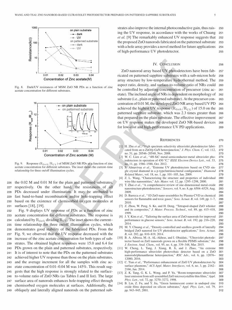
Fig. 8. Dark/UV resistances of MSM ZnO NR PDs as a function of zincacetate concentration for different substrates.
Fig. 9. Response (Rdark /RUV ) of MSM ZnO NR PDs as a function of zincacetate concentration for different substrates. The inset shows the current–timerelationship for three on/off illumination cycles.
the 0.02 M and 0.01 M for the plain and patterned substrates,226
respectively. On the other hand, the resistances of all227
PDs decreased under illumination. It may be attributed to228
fast band-to-band recombination and/or hole-trapping effect229
based on the existence of chemisorbed oxygen molecules at230
surfaces [18], [19].231
Fig. 9 displays UV response of PDs as a function of zinc232
acetate concentration for different substrates. The response is233
calculated by Rdark dividing RUV . The inset shows the current–234
time relationship for three on/off illumination cycles, which235
demonstrates good stability of the fabricated PDs. From the236
Fig. 9, we observed that the UV response decreased with the237
increase of the zinc acetate concentration for both types of sub-238
strates. The obtained highest responses were 15.0 and 6.4 for239
PDs grown on the plain and patterned substrates, respectively.240
It is of interest to note that the PDs on the patterned substrates241
achieved higher UV response than those on the plain substrates,242
and the average increment for all the samples with zinc ac-243
etate concentration of 0.01–0.04 M was 145%. This result sug-244
gests that the high response is strongly related to the surface-245
to-volume ratio of ZnO NRs (as Tables I and II list). The large246
surface area of nanorods enhances hole-trapping effect through247
chemisorbed oxygen molecules at surfaces. Additionally, the248
obliquely and laterally aligned nanorods on the patterned sub-249
strates also improve the internal photoconductive gain, thus rais- 250
ing the UV response, in accordance with the works of Chuang 251
et al. [9] The remarkably enhanced UV response suggests that 252
the proposed ZnO nanorods fabricated on the patterned substrate 253
with a hole array provides a novel method for future applications 254
of high-performance UV photodetector. 255
IV. CONCLUSION 256
ZnO nanorod array based UV photodetectors have been fab- 257
ricated on patterned sapphire substrates with a sub-micron hole 258
array structure by low-temperature hydrothermal method. The 259
aspect ratio, density, and surface-to-volume ratio of NRs could 260
be controlled by adjusting concentration of precursor (zinc ac- 261
etate). The inclined angle of NRs is dependent on morphology of 262
substrate (i.e., plain or patterned substrate). At the precursor con- 263
centration of 0.01 M, the developed ZnO NR array based UV PD 264
achieved the highest UV response (Rdark/RUV ) of 15.0 on the 265
patterned sapphire substrate, which was 2.3 times greater than 266
that prepared on the plain substrate. The effective improvement 267
on UV response makes the developed ZnO NR-based devices 268
for low-cost and high-performance UV PD applications. 269
REFERENCES 270
[1] H. Zhu et al., “High spectrum selectivity ultraviolet photodetector fabri- 271cated from an n-ZnO/p-GaN heterojunction,” J. Phys. Chem. C, vol. 112, 272no. 51, pp. 20546–20548, Nov. 2008. 273
[2] W. C. Lien et al., “4H-SiC metal-semiconductor-metal ultraviolet pho- 274todetectors in operation of 450 °C,” IEEE Electron Device Lett., vol. 33, 275no. 11, pp. 1586–1588, Oct. 2012. 276
[3] S. Almavivaa et al., “Extreme UV photodetectors based on CVD sin- 277gle crystal diamond in a p-type/intrinsic/metal configuration,” Diamond 278Related Mater., vol. 18, no. 1, pp. 101–105, Jan. 2009. 279
[4] Z. L. Wang, “Characterizing the structure and properties of individual 280wire-like nanoentities,” Adv. Mater. vol. 12, pp. 1295–1298, 2000. 281
[5] T. Zhai et al., “A comprehensive review of one-dimensional metal-oxide 282nanostructure photodetectors,” Sensors, vol. 9, no. 8, pp. 6504–6529, Aug. 2832009. 284
[6] D. Barreca et al., “1D ZnO nano-assemblies by Plasma-CVD as chemical 285sensors for flammable and toxic gases,” Sens. Actuat. B, vol. 149, pp. 1–7, 2862010. 287
[7] Z. Zhou, W. Peng, S. Ke, and H. Deng, “Tetrapod-shaped ZnO whisker 288and its composites,” J. Mater. Process. Technol., vol. 89, pp. 415–418, 2891999. 290
[8] J. Y. Kim et al., “Tailoring the surface area of ZnO nanorods for improved 291performance in glucose sensors,” Sens. Actuat. B, vol. 192, pp. 216–220, 2922014. 293
[9] M. Y. Chuang et al., “Density-controlled and seedless growth of laterally 294bridged ZnO nanorod for UV photodetector applications,” Sens. Actuat. 295B, vol. 202, pp. 810–819, 2014. 296
[10] B. A. Albissa, M.-A. AL-Akhras, and I. Obaidatc, “Ultraviolet photode- 297tector based on ZnO nanorods grown on a flexible PDMS substrate,” Int. 298J. Environ. Anal. Chem., vol. 95, no. 4, pp. 339–348, Mar. 2015. 299
[11] W. Cheng, L. Tang, J. Xiang, R. Ji, and J. Zhao, “An extreme 300high-performance ultraviolet photovoltaic detector based on a ZnO 301nanorods/phenanthrene heterojunction,” RSC Adv., vol. 6, pp. 12076– 30212080, 2016. 303
[12] C. Tian et al., “Performance enhancement of ZnO UV photodetectors by 304surface plasmons,” ACS Appl. Mater. Interfaces, vol. 6, no. 3, pp. 2162– 3052166, Jan. 2014. 306
[13] Z. K. Tang, G. K. L. Wong, and P. Yu, “Room-temperature ultraviolet 307laser emission from self-assembled ZnO microcrystallite thin films,” Appl. 308Phys. Lett., vol. 72, pp. 3270–3272, 1998. 309
[14] B. Lin, Z. Fu, and Y. Jia, “Green luminescent center in undoped zinc 310oxide films deposited on silicon substrates,” Appl. Phys. Lett., vol. 79, 311pp. 943–945, 2001. 312

IEEE P
roof
6 IEEE JOURNAL OF SELECTED TOPICS IN QUANTUM ELECTRONICS
[15] T. Singh, D. K. Pandya, and R. Singh, “Surface plasmon enhanced bandgap313emission of electrochemically grown ZnO nanorods using Au nanoparti-314cles,” Thin Solid Films, vol. 520, no. 14, pp. 4646–4649, May 2012.315
[16] B. A. Albiss, M.-A. AL-Akhras, and I. Obaidat, “Ultraviolet photodetector316based on ZnO nanorods grown on a flexible PDMS substrate,” Int. J.317Environ. Anal. Chem., vol. 95, no. 4, pp. 339–348, 2015.318
[17] P. Yang et al., “Controlled growth of ZnO nanowires and their optical319properties,” Adv. Funct. Mater. vol. 12, no. 5, pp. 323–331, May 2002.320
[18] J. D. Prades et al., Nanotechnology, vol. 19, 2008, Art. no. 465501.321[19] J. H. He, P. H. Chang, C. Y. Chen, and K. T. Tsai, “Electrical and opto-322
electronic characterization of a ZnO nanowire contacted by focused-ion-323beam-deposited Pt,” Nanotechnology, vol. 20, pp. 135701:1–135701:5,3242009.Q2 325
Fang-Hsing Wang (M’14) was born in Taiwan, in3261968. He received the B.S. and Ph.D. degrees in327electronic engineering from National Chiao-Tung328University, Hsinchu, Taiwan, in 1991 and 1997,329respectively.330
He was employed by Unipac Optoelectronic Cor-331poration from 1999–2001, where he researched and332developed technologies of TFT-LCDs. During 2002–3332003, he worked for Novatek Corporation to be an334IC designer for display driving ICs. In 2003, he335joined the faculty of National Chung-Hsing Univer-336
sity, Taichung, Taiwan, as an Assistant Professor. Since 2011, he has been an337Associate Professor in the Department of Electrical Engineering and Gradu-338ate Institute of Optoelectronic Engineering, National Chung-Hsing University,339Taichung, Taiwan. He is the author of more than 110 articles and 22 inventions.340His research interests include technologies of flat-panel displays and zinc oxide-341based thin-films and devices.342
Prof. Wang received the TACT International Conference Poster Paper Award343in 2011.344
345
Chih-En Tsai received the B.S. degree in electrical engineering from Yuan 346Ze University, Taoyuan, Taiwan, in 2012 and the M.S. degree in electrical 347engineering from National Chung Hsing University, Taichung, Taiwan, in 2015. 348His research interest includes the characteristics of ZnO nanorods, gas/UV light 349detectors, and the process and analysis of TCO films. 350
351

IEEE P
roof
QUERIES 352
Q1. Author: If you have not completed your electronic copyright form (ECF) and payment option please return to Scholar One 353
“Transfer Center.” In the Transfer Center you will click on “Manuscripts with Decisions” link. You will see your article 354
details and under the “Actions” column click “Transfer Copyright.” From the ECF it will direct you to the payment portal to 355
select your payment options and then return to ECF for copyright submission. 356
Q2. Author: Please provide article title in Ref. [18]. 357

IEEE P
roof
IEEE JOURNAL OF SELECTED TOPICS IN QUANTUM ELECTRONICS 1
ZnO Nanorod-Based Ultraviolet PhotodetectorPrepared on Patterned Sapphire Substrates
1
2
Fang-Hsing Wang, Member, IEEE, and Chih-En Tsai3
Abstract—A patterned sapphire substrate with a submicron holeQ1
4array structure was used to fabricate ZnO nanorod (NR) array5by low-temperature hydrothermal method. A ZnO seed layer was6spin-coated using sol-gel process and then etched to form sep-7arated seed islands. Different concentrations of zinc acetate in8the hydrothermal solution were performed for ZnO NR synthe-9sis to investigate ultraviolet (UV) photo-response properties. The10ZnO NRs synthesized on the patterned substrates were oriented11at various inclined angles. The diameter of the NRs increased and12their surface-to-volume ratio decreased as the concentrations of13zinc acetate increased from 0.01 to 0.04 M. X-ray diffraction and14photoluminescence analyses showed that the NRs synthesized in15a higher zinc acetate concentration had better crystal quality and16fewer defects. The current–voltage characteristics of the ZnO NR-17based metal-semiconductor-metal photodetectors exhibited a lin-18ear relationship, suggesting an Ohmic contact between NRs and19Al electrodes. The UV response, defined by the resistance ratio20(Rdark /RUV ), of the photodetectors increased with the decreasing21zinc acetate concentration from 0.04 to 0.01 M. Compared to tradi-22tional vertically aligned NR array on plain substrates, the proposed23ZnO NR-based photodetector on the patterned substrates achieved24improved UV responses, and the average increment for samples of250.01–0.04 M was 145%.26
Index Terms—ZnO nanorod, photodetectors, ultraviolet, nan-27otechnology, patterned substrate.28
I. INTRODUCTION29
U LTRAVIOLET (UV) photodetectors (PDs) have attracted30
increasing attention for last decade because of their wide31
applications in advanced communications, flame detection, air32
purification, ozone sensing and leak detection. UV photodetec-33
tors can be made based on wide band-gap semiconductor materi-34
als such as ZnO, GaN, SiC, SnO2 and diamond [1]–[3]. Among35
these materials, ZnO possesses certain unique properties, such36
as a direct band gap (3.37 eV), large exciton binding energy37
(60 meV), high thermal and chemical stability, transparence, and38
wide electrical conductivity range, and has become promising39
materials in applications of optoelectronic devices and sensors40
[4]. UV PDs come out based on the bulk, thin film or nanostruc-41
ture of the wide band-gap semiconductor materials. In general,42
the nanostructure materials have a higher photo responsivity43
because of scaling down of effective conductive channel and44
Manuscript received June 1, 2016; revised October 11, 2016; acceptedNovember 7, 2016. This work was supported in part by the Ministry of Scienceand Technology of Taiwan under Grant MOST 103-2221-E-005-040-MY2.
The authors are with the Department of Electrical Engineering andGraduate Institute of Optoelectronic Engineering, National Chung HsingUniversity, Taichung 402, Taiwan, R.O.C. (e-mail: [email protected]; [email protected]).
Color versions of one or more of the figures in this paper are available onlineat http://ieeexplore.ieee.org.
Digital Object Identifier 10.1109/JSTQE.2016.2630839
large surface to volume ratio. Especially, one-dimensional (1-D) 45
nanostructures have become a highlighted research topic in fab- 46
ricating electronic, optoelectronic, electrochemical, and elec- 47
tromechanical devices with nanoscale dimensions because of 48
their special shapes, compositions, and chemical, and physical 49
properties [5]. ZnO has many variety of different nanostructures, 50
including nanorods, nanowires, nanobelts, nanocombs, nanor- 51
ings, nanosprings, etc. Among them, 1-D ZnO nanorods (NRs) 52
prepared by hydrothermal reaction have been widely studied 53
because of advantages such as low cost and simple process 54
[6]–[12]. Kim et al. tailored the surface area of ZnO nanorods 55
by using different seed layers and precursor concentrations to 56
improve sensing performance [8]. Chuang et al. developed a 57
density-controlled and seedless growth method for laterally 58
bridged ZnO nanorods as a metal–semiconductor– metal pho- 59
todetector [9]. Their results indicated that highly dense lateral 60
ZnO nanorod-based PDs achieved a higher responsivity than 61
that with vertically aligned NRs. 62
In this study, we fabricated metal–semiconductor–metal 63
(MSM) ZnO nanorod-based UV PDs on a patterned concave 64
ZnO seed layer. The special seed layer was deposited on a sap- 65
phire substrate with a sub-micron honeycomb hole array struc- 66
ture using sol-gel spin-coating method. The UV response were 67
investigated particularly as a function of surface-to-volume ratio 68
of ZnO nanorods, which was tailored by the use of the patterned 69
seed layer and/or by changing the concentration of the precur- 70
sors in the hydrothermal growth solution. 71
II. EXPERIMENTS 72
Fig. 1 displays the flowchart of this experiment. The experi- 73
mental procedures for two types of substrates were: (a) devices 74
on flat glass or Si substrates: (1) cleaning substrates, (2) spin 75
coating ZnO seed layers by sol-gel method and then annealing 76
in Ar ambient at 500 °C for 1 h, (3) growing ZnO nanorod ar- 77
rays, (4) depositing aluminum interdigitated electrodes, and (b) 78
devices on patterned sapphire substrates: (1) cleaning substrate, 79
(2) depositing ZnO seed layers and then annealing in Ar ambient 80
at 500 °C for 1 h, (3) etching the seed layers to form separate 81
ZnO films by a dilute HCl solution (HCl:H2O = 1:1000) for 82
70 s, (4) growing ZnO nanorod arrays, (5) depositing aluminum 83
interdigitated electrodes. Fig. 2 exhibits the plan-view SEM im- 84
age of the patterned sapphire substrate with a sub-micron hole 85
array, which were brought from Shun-Hua Technology Inc. and 86
were fabricated via nanoimprint and etch method. The inset dis- 87
plays its cross sectional view. The hole pitch, height, and bottom 88
diameter were about 1.5, 0.5, and 0.3 μm, respectively. 89
The ZnO nanorod arrays were synthesized by hydrother- 90
mal method on seeded Corning eagle XG glass and patterned 91
1077-260X © 2016 IEEE. Personal use is permitted, but republication/redistribution requires IEEE permission.See http://www.ieee.org/publications standards/publications/rights/index.html for more information.

IEEE P
roof
2 IEEE JOURNAL OF SELECTED TOPICS IN QUANTUM ELECTRONICS
Fig. 1. Schematic flowchart of this experiment. The experimental procedurefor the two types of devices: (a) PDs grown on patterned sapphire substrates,(b) PDs grown on plain Si (or glass) substrates.
Fig. 2. Plan-view SEM image of the patterned sapphire substrate with a sub-micron hole array. The inset displays its cross sectional view.
sapphire substrates. First, substrates were cleaned by super-92
sonic bath in deionized water, acetone, and isopropyl alco-93
hol sequentially. Second ZnO seed layers were deposited by94
sol–gel spin coating method. Then the ZnO seed layer on sap-95
phire was etched by dilute hydrochloric acid to produce a pat-96
terned ZnO seed layer array. The source solutions for ZnO97
nanorods growth was prepared with the precursors, zinc acetate98
dehydrate Zn(C2H3O2)2 ·2H2O and Hexamethylenetetramine99
(HMTA) C6H12N4 as modifying agent in stoichiometric pro-100
portions dissolving in de-ionized water. The concentrations of101
zinc acetate solution (0.01–0.04 M) with the growth time of102
60 min were performed to grow ZnO nanorods.103
Fig. 3. Plan-view and cross-section FE-SEM images of the ZnO seed layergrown on different substrates: (a), (b) plane substrate, (c), (d) patterned sapphiresubstrate before wet etching, and (c), (f) patterned sapphire substrate after wetetching.
The X-ray diffraction (XRD, PANalytical) with Cu–Kα radi- 104
ation (λ = 1.54056 A, θ–2θ scan mode) was used to characterize 105
structural and crystallographic properties of the ZnO nanorods. 106
Surface morphologies and size distribution of the ZnO nanorods 107
were characterized by a field-emission scanning electron micro- 108
scope (FE-SEM, JEOL, JSM–6700F). Photoluminescence (PL) 109
spectroscopy (Horiba, iHR550) was employed at room temper- 110
ature using a 325 nm He–Cd laser for the investigation of optical 111
emission properties. 112
Finally, Al interdigitated electrodes with a thickness of 113
350 nm were deposited on the ZnO nanorod array using thermal 114
evaporation to form metal-semiconductor-metal (MSM) pho- 115
todetectors (PDs). The dark/photo currents were determined 116
using a Keithley 2400 source meter interfaced with a computer 117
under illumination from a 365 nm UV LED at RT in ambient 118
atmosphere. 119
III. RESULTS AND DISCUSSION 120
A. Growth of ZnO Nanorod Array 121
Fig. 3 shows plan-view and cross-section FE-SEM images 122
of the ZnO seed layer grown on different substrates: (a, b) 123
glass, (c, d) sapphire before wet etching, and (e, f) sapphire 124
after wet etching. From the Fig. 3(a), the thickness of the ZnO 125
seed layer grown by sol-gel method was about 220 nm, and their 126
surface particle size was about 30 nm. For the patterned sapphire 127
substrates, we observed that the continuous seed layer on the 128
concave surface had been separated into many independent seed 129
islands in each comb-like hole after wet etching (see Fig. 3(e). 130

IEEE P
roof
WANG AND TSAI: ZNO NANOROD-BASED ULTRAVIOLET PHOTODETECTOR PREPARED ON PATTERNED SAPPHIRE SUBSTRATES 3
Fig. 4. Plan-view and cross-section FE-SEM images of the ZnO nanorods:(a), (b) 0.01 M grown on plain Si substrates, (c), (d) 0.01 M grown on patternedsapphire substrates, (e), (f) 0.03 M grown on patterned sapphire substrates.
TABLE ISTRUCTURES OF ZNO NRS GROWN ON SI SUBSTRATES WITH DIFFERENT
CONCENTRATION OF ZINC ACETATE
Concentration of zinc acetate (M) 0.01 0.02 0.03 0.04
Diameter (nm) 50 60 95 150Length (nm) 1600 1700 1650 1630Density of ZnO NRs (μm−2) 100 110 85 40Total surface area of ZnO NRson 1 μm2 seed layer (μm2)
25.32 35.54 42.44 31.41
Total volume of ZnO NRs on 1μm2 seed layer (μm2)
0.31 0.53 0.99 1.15
Surface-to-volume ratio 81.7 67.1 42.9 27.3
Fig. 4(a)–(f) displays plan-view and cross-section FE-SEM131
images of ZnO nanorod array grown on different substrates. The132
typical vertically well-aligned ZnO nanorod array can be found133
on plain seeded substrates, as Fig. 4(a) and 4(b) shows. However,134
on the patterned substrate with a hole array, growth orientation135
of ZnO nanorods depended on the seed pattern and surface mor-136
phology of the substrate. Some of nanorods exhibited obliquely137
or laterally aligned structure instead of vertical ones (see138
Fig. 4 (c)–(f)). Besides, as comparing the nanorods grown139
with different concentration of the precursor, we found that140
the stronger precursor concentration, the thicker and longer141
nanorods were. The estimated structural parameters of ZnO142
nanorods grown on plane Si substrates and patterned sapphire143
substrates with different concentration of zinc acetate with144
growth time of 60 min were list in Table I and Table II. The145
diameter and total volume of ZnO nanorods both increased146
monotonically with the increase of the concentration of zinc147
TABLE IISTRUCTURES OF ZNO NRS GROWN ON SAPPHIRE SUBSTRATES WITH
DIFFERENT CONCENTRATION OF ZINC ACETATE
Concentration of zinc acetate (M) 0.01 0.02 0.03 0.04
Diameter (nm) 30 50 90 140Length (nm) 900 1650 1700 1250Density of ZnO NRs (μm−2) 105 60 65 50Total surface area of ZnO NRson 1 μm2 seed layer (μm2)
7.99 15.66 31.64 28.24
Total volume of ZnO NRs on 1μm2 seed layer (μm2)
0.06 0.19 0.70 0.96
Surface-to-volume ratio 133.2 82.4 45.2 29.4
Fig. 5. θ−2θ XRD patterns of ZnO nanorods prepared on (a) plain glasssubstrates and (b) patterned sapphire substrates as a function of zinc acetateconcentration.
acetate regardless of substrate type. The total surface area of 148
ZnO nanorods increased and then decreased with the concen- 149
tration of zinc acetate, and the maximum surface area was found 150
with zinc acetate solution of 0.03 M. In comparison, the ZnO 151
nanorods grown on the plain substrate had larger diameters and 152
the total surface area than the other. It may be due the better 153
crystal quality of the seed layer on the plain substrate because 154
of without undergoing the etch process. The surface-to-volume 155
ratio decreased with the increasing the concentration of zinc 156
acetate for the both types of samples, and it was worth noting 157
that the largest ratio (133.2) was achieved for 0.01 M on the 158
patterned sapphire substrate. 159
Fig. 5 presents θ–2θ XRD patterns of ZnO nanorods as a 160
function of concentration of zinc acetate in the hydrothermal 161
solution. As seen in Fig. 5(a) and (b), all the ZnO nanorods 162
exhibited polycrystalline nature with a highly (002) preferred 163
orientation along the c-axis, indicating a typical wurtzite struc- 164
ture. The peak intensity increased as the concentration of zinc 165
acetate increased, suggesting that the (002) peak intensity in- 166
creased with the increase of the total volume of ZnO NRs. Com- 167
pared to the ZnO nanorods on the patterned sapphire substrate, 168
nanorods on the plain substrate possessed higher (002) peak 169
intensity, revealing larger volume and better crystallinity. This 170
result is consistent with the findings in the FE-SEM observation 171
(Fig. 4). 172

IEEE P
roof
4 IEEE JOURNAL OF SELECTED TOPICS IN QUANTUM ELECTRONICS
Fig. 6. Photoluminescence spectra of ZnO nanorods grown on (a) plain Sisubstrates and (b) patterned sapphire substrates.
Photoluminescence (PL) spectra of ZnO nanorods grown on173
different substrates are shown in Fig. 6. All samples exhibited174
two emission bands. The sharp UV emission band centered at175
around 374.4 nm corresponded to the near-band-edge emission176
and free-exciton peak of ZnO [13]. The broad green emission177
bands in the visible region were located at around 460–570 nm178
and were referred to as the intrinsic defects (e.g., oxygen va-179
cancy and zinc interstitials) and crystal defects (e.g., lumines-180
cent centers) in the ZnO [14]–[16]. The insets list the intensities181
of the UV emission peak (IUV ) and the green emission band182
(IG ), as well as ratios of IG/IUV . Clearly, the NRs prepared183
with the precursor concentration of 0.03 M show enhanced UV184
emission and weakened green emission compared with those185
using 0.01 M regardless of substrate morphology. This is con-186
sistent with the results reported by Yang et al., in which they187
found that the green emission relative to the UV emission in-188
creased as the nanowire diameter decreased [17]. The intensity189
ratio between green emission and UV emission bands (IG/IUV ),190
which generally indicates the relative defect amount in ZnO, was191
smaller for the 0.03 M samples, revealing the less surface de-192
fects and higher crystal quality of the developed ZnO NRs in193
this condition [9].194
B. Characteristics of UV Photodetectors195
The MSM UV PDs were fabricated by evaporating Al inter-196
digitated electrodes on ZnO nanorod array. Fig. 7 show I–V char-197
acteristics of the MSM PDs in dark and under UV illumination198
Fig. 7. (a) Dark and (b) photo currents of MSM ZnO NR PDs as a functionof voltage for different concentration and substrates.
for different substrates. The observed highly linear relationship 199
in the I–V characteristics demonstrated a good Ohmic contact 200
property at the ZnO NRs and Al electrodes interface regardless 201
of illumination and substrate type. Since the electron affinity 202
of ZnO (χZnO = 4.35 eV) is higher than the work function of 203
Al (ΦAl = 4.25 eV), an Ohmic contact would be expected to 204
form as Al electrodes are deposited on ZnO nanorods. At 5.0 V 205
voltage bias, the dark and photo currents of the 0.01 M device 206
on the patterned substrate were 9.65 and 162 μA. The dark 207
current corresponds to the leakage current of the MSM PDs. 208
In dark ambient, oxygen molecules absorb on ZnO nanorod 209
surface and capture free electrons, and a depletion region is 210
formed near the surface, leading to a low current. Upon UV 211
illumination, electron–hole pairs are photo-generated, and then 212
holes are readily trapped at the surface or combined with nega- 213
tively charged absorbed oxygen ions, leaving behind electrons 214
in the nanorods that transport to anodes and contribute to the 215
high photocurrent. It is clear that the ZnO nanorod-based PDs 216
is highly sensitive to UV light, and the photocurrent increases 217
by approximate16 times of magnitude compared to the dark 218
current. The dark and photo resistances could be calculated as 219
518 and 30.9 kΩ, respectively for this device. Fig. 8 presents 220
calculated dark and UV resistances of PDs as a function of 221
zinc acetate concentration. The resistance of PDs gradually 222
decreased as the concentration of zinc acetate increased be- 223
cause of the thick nanorods and the improved crystallinity at 224
the high concentration. The maximum of resistance occurred at 225
IEEE P
roof
WANG AND TSAI: ZNO NANOROD-BASED ULTRAVIOLET PHOTODETECTOR PREPARED ON PATTERNED SAPPHIRE SUBSTRATES 5
Fig. 8. Dark/UV resistances of MSM ZnO NR PDs as a function of zincacetate concentration for different substrates.
Fig. 9. Response (Rdark /RUV ) of MSM ZnO NR PDs as a function of zincacetate concentration for different substrates. The inset shows the current–timerelationship for three on/off illumination cycles.
the 0.02 M and 0.01 M for the plain and patterned substrates,226
respectively. On the other hand, the resistances of all227
PDs decreased under illumination. It may be attributed to228
fast band-to-band recombination and/or hole-trapping effect229
based on the existence of chemisorbed oxygen molecules at230
surfaces [18], [19].231
Fig. 9 displays UV response of PDs as a function of zinc232
acetate concentration for different substrates. The response is233
calculated by Rdark dividing RUV . The inset shows the current–234
time relationship for three on/off illumination cycles, which235
demonstrates good stability of the fabricated PDs. From the236
Fig. 9, we observed that the UV response decreased with the237
increase of the zinc acetate concentration for both types of sub-238
strates. The obtained highest responses were 15.0 and 6.4 for239
PDs grown on the plain and patterned substrates, respectively.240
It is of interest to note that the PDs on the patterned substrates241
achieved higher UV response than those on the plain substrates,242
and the average increment for all the samples with zinc ac-243
etate concentration of 0.01–0.04 M was 145%. This result sug-244
gests that the high response is strongly related to the surface-245
to-volume ratio of ZnO NRs (as Tables I and II list). The large246
surface area of nanorods enhances hole-trapping effect through247
chemisorbed oxygen molecules at surfaces. Additionally, the248
obliquely and laterally aligned nanorods on the patterned sub-249
strates also improve the internal photoconductive gain, thus rais- 250
ing the UV response, in accordance with the works of Chuang 251
et al. [9] The remarkably enhanced UV response suggests that 252
the proposed ZnO nanorods fabricated on the patterned substrate 253
with a hole array provides a novel method for future applications 254
of high-performance UV photodetector. 255
IV. CONCLUSION 256
ZnO nanorod array based UV photodetectors have been fab- 257
ricated on patterned sapphire substrates with a sub-micron hole 258
array structure by low-temperature hydrothermal method. The 259
aspect ratio, density, and surface-to-volume ratio of NRs could 260
be controlled by adjusting concentration of precursor (zinc ac- 261
etate). The inclined angle of NRs is dependent on morphology of 262
substrate (i.e., plain or patterned substrate). At the precursor con- 263
centration of 0.01 M, the developed ZnO NR array based UV PD 264
achieved the highest UV response (Rdark/RUV ) of 15.0 on the 265
patterned sapphire substrate, which was 2.3 times greater than 266
that prepared on the plain substrate. The effective improvement 267
on UV response makes the developed ZnO NR-based devices 268
for low-cost and high-performance UV PD applications. 269
REFERENCES 270
[1] H. Zhu et al., “High spectrum selectivity ultraviolet photodetector fabri- 271cated from an n-ZnO/p-GaN heterojunction,” J. Phys. Chem. C, vol. 112, 272no. 51, pp. 20546–20548, Nov. 2008. 273
[2] W. C. Lien et al., “4H-SiC metal-semiconductor-metal ultraviolet pho- 274todetectors in operation of 450 °C,” IEEE Electron Device Lett., vol. 33, 275no. 11, pp. 1586–1588, Oct. 2012. 276
[3] S. Almavivaa et al., “Extreme UV photodetectors based on CVD sin- 277gle crystal diamond in a p-type/intrinsic/metal configuration,” Diamond 278Related Mater., vol. 18, no. 1, pp. 101–105, Jan. 2009. 279
[4] Z. L. Wang, “Characterizing the structure and properties of individual 280wire-like nanoentities,” Adv. Mater. vol. 12, pp. 1295–1298, 2000. 281
[5] T. Zhai et al., “A comprehensive review of one-dimensional metal-oxide 282nanostructure photodetectors,” Sensors, vol. 9, no. 8, pp. 6504–6529, Aug. 2832009. 284
[6] D. Barreca et al., “1D ZnO nano-assemblies by Plasma-CVD as chemical 285sensors for flammable and toxic gases,” Sens. Actuat. B, vol. 149, pp. 1–7, 2862010. 287
[7] Z. Zhou, W. Peng, S. Ke, and H. Deng, “Tetrapod-shaped ZnO whisker 288and its composites,” J. Mater. Process. Technol., vol. 89, pp. 415–418, 2891999. 290
[8] J. Y. Kim et al., “Tailoring the surface area of ZnO nanorods for improved 291performance in glucose sensors,” Sens. Actuat. B, vol. 192, pp. 216–220, 2922014. 293
[9] M. Y. Chuang et al., “Density-controlled and seedless growth of laterally 294bridged ZnO nanorod for UV photodetector applications,” Sens. Actuat. 295B, vol. 202, pp. 810–819, 2014. 296
[10] B. A. Albissa, M.-A. AL-Akhras, and I. Obaidatc, “Ultraviolet photode- 297tector based on ZnO nanorods grown on a flexible PDMS substrate,” Int. 298J. Environ. Anal. Chem., vol. 95, no. 4, pp. 339–348, Mar. 2015. 299
[11] W. Cheng, L. Tang, J. Xiang, R. Ji, and J. Zhao, “An extreme 300high-performance ultraviolet photovoltaic detector based on a ZnO 301nanorods/phenanthrene heterojunction,” RSC Adv., vol. 6, pp. 12076– 30212080, 2016. 303
[12] C. Tian et al., “Performance enhancement of ZnO UV photodetectors by 304surface plasmons,” ACS Appl. Mater. Interfaces, vol. 6, no. 3, pp. 2162– 3052166, Jan. 2014. 306
[13] Z. K. Tang, G. K. L. Wong, and P. Yu, “Room-temperature ultraviolet 307laser emission from self-assembled ZnO microcrystallite thin films,” Appl. 308Phys. Lett., vol. 72, pp. 3270–3272, 1998. 309
[14] B. Lin, Z. Fu, and Y. Jia, “Green luminescent center in undoped zinc 310oxide films deposited on silicon substrates,” Appl. Phys. Lett., vol. 79, 311pp. 943–945, 2001. 312

IEEE P
roof
6 IEEE JOURNAL OF SELECTED TOPICS IN QUANTUM ELECTRONICS
[15] T. Singh, D. K. Pandya, and R. Singh, “Surface plasmon enhanced bandgap313emission of electrochemically grown ZnO nanorods using Au nanoparti-314cles,” Thin Solid Films, vol. 520, no. 14, pp. 4646–4649, May 2012.315
[16] B. A. Albiss, M.-A. AL-Akhras, and I. Obaidat, “Ultraviolet photodetector316based on ZnO nanorods grown on a flexible PDMS substrate,” Int. J.317Environ. Anal. Chem., vol. 95, no. 4, pp. 339–348, 2015.318
[17] P. Yang et al., “Controlled growth of ZnO nanowires and their optical319properties,” Adv. Funct. Mater. vol. 12, no. 5, pp. 323–331, May 2002.320
[18] J. D. Prades et al., Nanotechnology, vol. 19, 2008, Art. no. 465501.321[19] J. H. He, P. H. Chang, C. Y. Chen, and K. T. Tsai, “Electrical and opto-322
electronic characterization of a ZnO nanowire contacted by focused-ion-323beam-deposited Pt,” Nanotechnology, vol. 20, pp. 135701:1–135701:5,3242009.Q2 325
Fang-Hsing Wang (M’14) was born in Taiwan, in3261968. He received the B.S. and Ph.D. degrees in327electronic engineering from National Chiao-Tung328University, Hsinchu, Taiwan, in 1991 and 1997,329respectively.330
He was employed by Unipac Optoelectronic Cor-331poration from 1999–2001, where he researched and332developed technologies of TFT-LCDs. During 2002–3332003, he worked for Novatek Corporation to be an334IC designer for display driving ICs. In 2003, he335joined the faculty of National Chung-Hsing Univer-336
sity, Taichung, Taiwan, as an Assistant Professor. Since 2011, he has been an337Associate Professor in the Department of Electrical Engineering and Gradu-338ate Institute of Optoelectronic Engineering, National Chung-Hsing University,339Taichung, Taiwan. He is the author of more than 110 articles and 22 inventions.340His research interests include technologies of flat-panel displays and zinc oxide-341based thin-films and devices.342
Prof. Wang received the TACT International Conference Poster Paper Award343in 2011.344
345
Chih-En Tsai received the B.S. degree in electrical engineering from Yuan 346Ze University, Taoyuan, Taiwan, in 2012 and the M.S. degree in electrical 347engineering from National Chung Hsing University, Taichung, Taiwan, in 2015. 348His research interest includes the characteristics of ZnO nanorods, gas/UV light 349detectors, and the process and analysis of TCO films. 350
351

IEEE P
roof
QUERIES 352
Q1. Author: If you have not completed your electronic copyright form (ECF) and payment option please return to Scholar One 353
“Transfer Center.” In the Transfer Center you will click on “Manuscripts with Decisions” link. You will see your article 354
details and under the “Actions” column click “Transfer Copyright.” From the ECF it will direct you to the payment portal to 355
select your payment options and then return to ECF for copyright submission. 356
Q2. Author: Please provide article title in Ref. [18]. 357