Embed Size (px)
Citation preview
2019/12/3
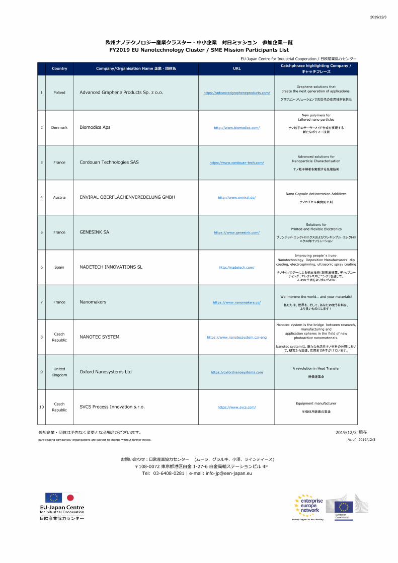
Country Company/Organisation Name 企業・団体名 URLCatchphrase highlighting Company /
キャッチフレーズ
1 Poland Advanced Graphene Products Sp. z o.o. https://advancedgrapheneproducts.com/
Graphene solutions that
create the next generation of applications.
グラフェン・ソリューションで次世代の応用技術を創出
2 Denmark Biomodics Aps http://www.biomodics.com/
New polymers for
tailored nano particles
ナノ粒子のテーラーメイド合成を実現する
新たなポリマー技術
3 France Cordouan Technologies SAS https://www.cordouan-tech.com/
Advanced solutions for
Nanoparticle Characterisation
ナノ粒子解析を実現する先端技術
4 Austria ENVIRAL OBERFLÄCHENVEREDELUNG GMBH http://www.enviral.de/Nano Capsule Anticorrosion Additives
ナノカプセル腐食防止剤
5 France GENESINK SA https://www.genesink.com/
Solutions for
Printed and Flexible Electronics
プリンテッド・エレクトロニクスおよびフレキシブル・エレクトロニクス向けソリューション
6 Spain NADETECH INNOVATIONS SL http://nadetech.com/
Improving people´s lives-
Nanotechnology Deposition Manufacturers: dip
coating, electrospinning, ultrasonic spray coating
ナノテクノロジーによる析出技術(超音波噴霧、ディップコーティング、エレクトロスピニング)を通じて、
人々の生活をより良いものに
7 France Nanomakers https://www.nanomakers.co/
We improve the world… and your materials!
私たちは、世界を、そして、あなたの使う材料を、より良いものにします!
8Czech
RepublicNANOTEC SYSTEM https://www.nanotecsystem.cz/-eng
Nanotec system is the bridge between research,
manufacturing and
application spheres in the field of new
photoactive nanomaterials.
Nanotec systemは、新たな光活性ナノ材料の分野において、研究から製造、応用までを手がけています。
9United
KingdomOxford Nanosystems Ltd https://oxfordnanosystems.com
A revolution in Heat Transfer
熱伝達革命
10Czech
RepublicSVCS Process Innovation s.r.o. https://www.svcs.com/
Equipment manufacturer
半導体用装置の製造
2019/12/3 現在
As of 2019/12/3
お問い合わせ:日欧産業協力センター (ムーラ、グラルキ、小澤、ラインティース)
〒108-0072 東京都港区白金 1-27-6 白金高輪ステーションビル 4F
Tel: 03-6408-0281 | e-mail: [email protected]
欧州ナノテクノロジー産業クラスター・中小企業 対日ミッション 参加企業一覧
FY2019 EU Nanotechnology Cluster / SME Mission Participants List
EU-Japan Centre for Industrial Cooperation / 日欧産業協力センター
参加企業・団体は予告なく変更となる場合がございます。
participating companies/ organisations are subject to change without further notice.
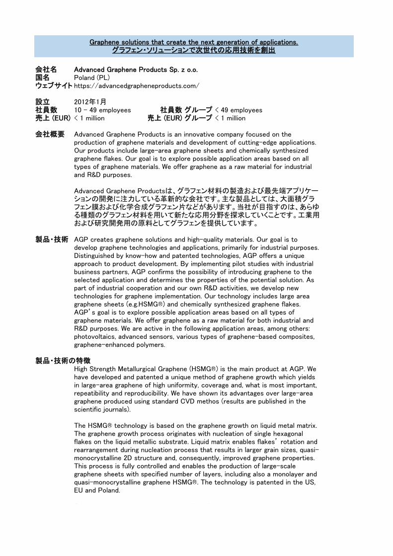
会社名国名ウェブサイト https://advancedgrapheneproducts.com/
設立社員数 10 - 49 employees 社員数 グループ < 49 employees売上 (EUR) 売上 (EUR) グループ < 1 million
会社概要
製品・技術
製品・技術の特徴
Graphene solutions that create the next generation of applications.グラフェン・ソリューションで次世代の応用技術を創出
Advanced Graphene Products is an innovative company focused on theproduction of graphene materials and development of cutting-edge applications.Our products include large-area graphene sheets and chemically synthesizedgraphene flakes. Our goal is to explore possible application areas based on alltypes of graphene materials. We offer graphene as a raw material for industrialand R&D purposes.
Advanced Graphene Productsは、グラフェン材料の製造および最先端アプリケーションの開発に注力している革新的な会社です。主な製品としては、大面積グラフェン膜および化学合成グラフェン片などがあります。当社が目指すのは、あらゆる種類のグラフェン材料を用いて新たな応用分野を探求していくことです。工業用および研究開発用の原料としてグラフェンを提供しています。
AGP creates graphene solutions and high-quality materials. Our goal is todevelop graphene technologies and applications, primarily for industrial purposes.Distinguished by know-how and patented technologies, AGP offers a uniqueapproach to product development. By implementing pilot studies with industrialbusiness partners, AGP confirms the possibility of introducing graphene to theselected application and determines the properties of the potential solution. Aspart of industrial cooperation and our own R&D activities, we develop newtechnologies for graphene implementation. Our technology includes large areagraphene sheets (e.g.HSMG®) and chemically synthesized graphene flakes.AGP’s goal is to explore possible application areas based on all types ofgraphene materials. We offer graphene as a raw material for both industrial andR&D purposes. We are active in the following application areas, among others:photovoltaics, advanced sensors, various types of graphene-based composites,graphene-enhanced polymers.
High Strength Metallurgical Graphene (HSMG®) is the main product at AGP. Wehave developed and patented a unique method of graphene growth which yieldsin large-area graphene of high uniformity, coverage and, what is most important,repeatibility and reproducibility. We have shown its advantages over large-areagraphene produced using standard CVD methos (results are published in thescientific journals).
The HSMG® technology is based on the graphene growth on liquid metal matrix.The graphene growth process originates with nucleation of single hexagonalflakes on the liquid metallic substrate. Liquid matrix enables flakes’ rotation andrearrangement during nucleation process that results in larger grain sizes, quasi-monocrystalline 2D structure and, consequently, improved graphene properties.This process is fully controlled and enables the production of large-scalegraphene sheets with specified number of layers, including also a monolayer andquasi-monocrystalline graphene HSMG®. The technology is patented in the US,EU and Poland.
AGP holds other patents and has also filed for new patents focused on other
Advanced Graphene Products Sp. z o.o.Poland (PL)
2012年1月
< 1 million
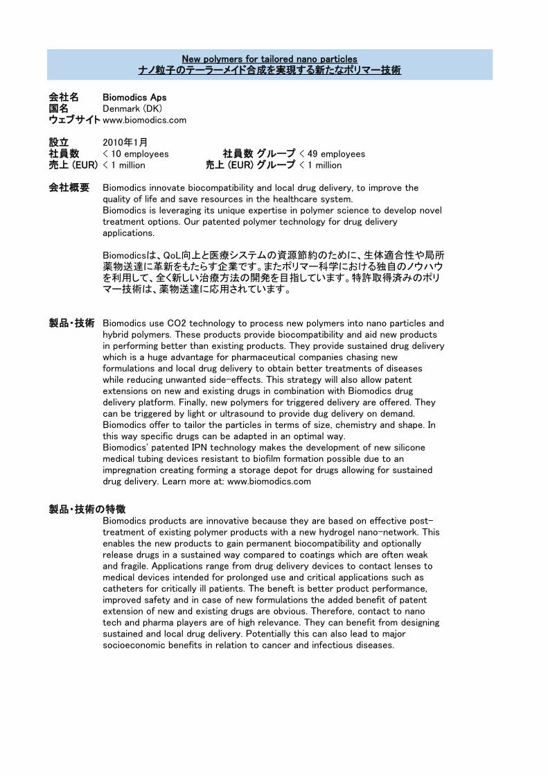
会社名国名ウェブサイト www.biomodics.com
設立社員数 < 10 employees 社員数 グループ < 49 employees売上 (EUR) 売上 (EUR) グループ < 1 million
会社概要
製品・技術
製品・技術の特徴
New polymers for tailored nano particlesナノ粒子のテーラーメイド合成を実現する新たなポリマー技術
Biomodics innovate biocompatibility and local drug delivery, to improve thequality of life and save resources in the healthcare system.Biomodics is leveraging its unique expertise in polymer science to develop noveltreatment options. Our patented polymer technology for drug deliveryapplications.
Biomodicsは、QoL向上と医療システムの資源節約のために、生体適合性や局所薬物送達に革新をもたらす企業です。またポリマー科学における独自のノウハウを利用して、全く新しい治療方法の開発を目指しています。特許取得済みのポリマー技術は、薬物送達に応用されています。
Biomodics use CO2 technology to process new polymers into nano particles andhybrid polymers. These products provide biocompatibility and aid new productsin performing better than existing products. They provide sustained drug deliverywhich is a huge advantage for pharmaceutical companies chasing newformulations and local drug delivery to obtain better treatments of diseaseswhile reducing unwanted side-effects. This strategy will also allow patentextensions on new and existing drugs in combination with Biomodics drugdelivery platform. Finally, new polymers for triggered delivery are offered. Theycan be triggered by light or ultrasound to provide dug delivery on demand.Biomodics offer to tailor the particles in terms of size, chemistry and shape. Inthis way specific drugs can be adapted in an optimal way.Biomodics' patented IPN technology makes the development of new siliconemedical tubing devices resistant to biofilm formation possible due to animpregnation creating forming a storage depot for drugs allowing for sustaineddrug delivery. Learn more at: www.biomodics.com
Biomodics products are innovative because they are based on effective post-treatment of existing polymer products with a new hydrogel nano-network. Thisenables the new products to gain permanent biocompatibility and optionallyrelease drugs in a sustained way compared to coatings which are often weakand fragile. Applications range from drug delivery devices to contact lenses tomedical devices intended for prolonged use and critical applications such ascatheters for critically ill patients. The beneft is better product performance,improved safety and in case of new formulations the added benefit of patentextension of new and existing drugs are obvious. Therefore, contact to nanotech and pharma players are of high relevance. They can benefit from designingsustained and local drug delivery. Potentially this can also lead to majorsocioeconomic benefits in relation to cancer and infectious diseases.
Biomodics ApsDenmark (DK)
2010年1月
< 1 million
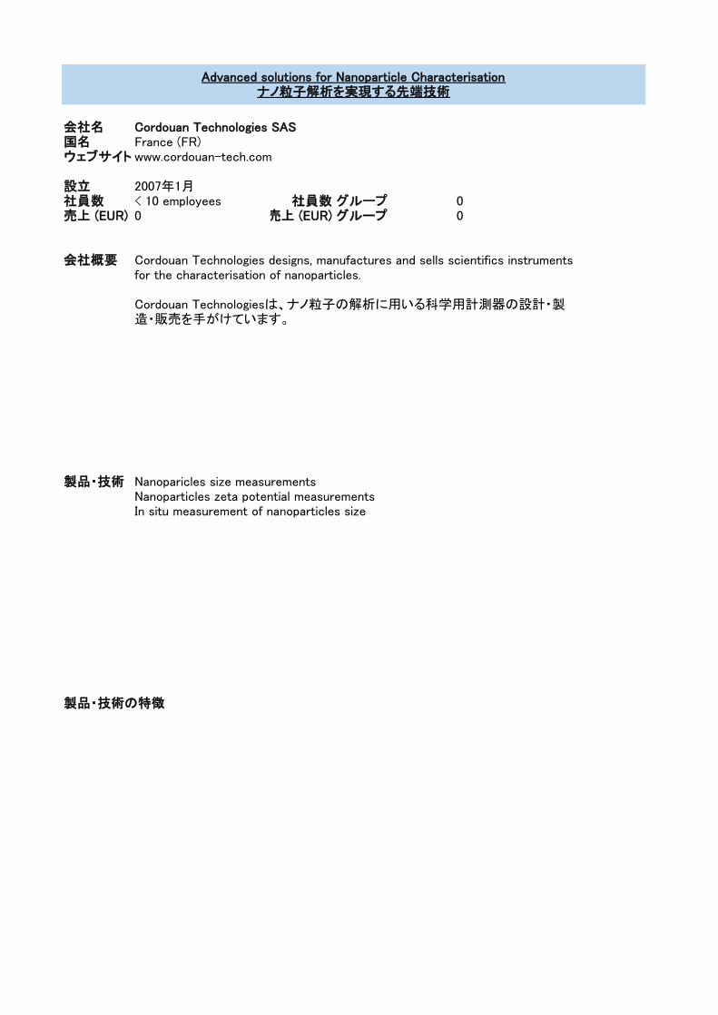
会社名国名ウェブサイト www.cordouan-tech.com
設立社員数 < 10 employees 社員数 グループ 0売上 (EUR) 売上 (EUR) グループ 0
会社概要
製品・技術
製品・技術の特徴
Cordouan Technologies designs, manufactures and sells scientifics instrumentsfor the characterisation of nanoparticles.
Cordouan Technologiesは、ナノ粒子の解析に用いる科学用計測器の設計・製造・販売を手がけています。
Nanoparicles size measurementsNanoparticles zeta potential measurementsIn situ measurement of nanoparticles size
Advanced solutions for Nanoparticle Characterisationナノ粒子解析を実現する先端技術
Cordouan Technologies SASFrance (FR)
2007年1月
0
会社名国名ウェブサイト http://www.enviral.de/
設立社員数 10 - 49 employees 社員数 グループ 0売上 (EUR) 売上 (EUR) グループ 1 to 10
会社概要
製品・技術
製品・技術の特徴
The SmartCorr product developed by ENVIRAL is based on fundamentalresearch by the Max-Planck-Institute which has been patented and exclusivelylicensed to ENVIRAL by Max-Planck-Innovation GmbH. In line with the self-healing mechanism of human skin, we developed an innovative process tofunctionalise corrosion protection coatings in order to also allow them to healdamage autonomously.
ENVIRALが開発を手がけるSmartCorr製品は、マックス・プランク研究所による基礎研究に基づいています。同研究の成果は、Max-Planck-Innovation GmbHが特許を取得し、ENVIRALにその独占的使用権が認められています。人間の皮膚がもつ自己修復作用を利用して、自律的な損傷修復も可能な防食被膜機能を実現する革新的な方法を開発しました。
We develop and produce anticorrosion additives base on a new technology ofnanoencapsulation, such additives added to dry and wet pints significantlyprolong the resistance of material to corrosion growth. According to our tests,the single coated layer with our additives can show the similar anticorrosioncharacteristics kike double coated layers without additives. Therefore, theeconomical saving are obvious.
Nano Capsule Anticorrosion Additivesナノカプセル腐食防止剤
ENVIRAL OBERFLÄCHENVEREDELUNG GMBHGermany
1994年1月
1 to 10
会社名国名ウェブサイト https://www.genesink.com/
設立社員数 < 10 employees 社員数 グループ < 49 employees売上 (EUR) 売上 (EUR) グループ < 1 million
会社概要 GenesInk is a world leader in advanced materials and formulations for theprinted & flexible electronics market. Our solutions of conductive and semi-conductive inks bring competitive advantages to industries looking for thin andflexible devices, high conductivity and outstanding electrical performances.
Since GenesInk creation we have been strongly networking and cooperating withthe industry and all related R&D centers and universities. This has enabled us toexchange product needs and test data with more than one thousand companiesand R&D centers. Based on that global network with direct users and OEMs weare able to collect strategic, marketing and technical information that are one ofthe pillar of our innovation: listening to our customers.
Multiple approaches are used to develop and market new products:・Understanding new products developments needs: our world class scientificcommittee is guiding the technological roadmap.・Listening to customers technical needs and specifications: Customer intimacyenables GenesInk to fine tune existing formulas to the exact needs of theprocess (beta customers testing).・Cooperating with R&D centers and key industry players: Acting as formulatorsin the development of new electronic products enable GenesInk to understandfuture needs and constraints.
Our patented technologies are successfully used in applications such as:・Integrated Smart Systems・In Mold Electronics・Thin and Large Area Electronics: OPV, OLED・Transparent conductive films for displays
Our inks are compatible with industrial printing methods and flexible substratesfor large scale production.
GenesInk is a company based in the south of France, in the area of Aix-En-Provence. It has a global distribution network and a sales office in Tokyo, Japanand USA. As an active company in the field of innovation, GenesInk is part ofthe H2020 European research program. Ongoing projects focus on ITO-freeelectrodes manufacturing and flexible batteries.
GenesInkは、プリンテッド・エレクトロニクス市場およびフレキシブル・エレクトロニクス市場で用いられる高性能素材・モデルの分野において、世界をリードする企業です。導電性や半導体性をもつインクによって、薄くてフレキシブルな機器や高い導電性と卓越した電気的性能を求める業界に競争力をもたらします。
GenesInkは設立以来、業界および関連R&Dセンターや大学と緊密に連携し、協働してきました。これにより、1,000を超す企業やR&Dセンターとの間で、製品ニーズやテストデータの交換が行われてきました。
世界中のダイレクトユーザーやOEM業者とのネットワークを活かして、当社のイノベーションを支える柱の一つともいえる「顧客の声を聞く」ことを通じて、戦略的情報・市場情報・技術情報の収集が可能となっています。
新製品の開発・販売には、複数の手法が用いられています。・新製品開発に対するニーズの把握:世界最高レベルの当社科学委員会が、技術ロードマップの作成を主導しています。・顧客の技術的ニーズや仕様ニーズの把握:顧客のニーズを深く理解することにより、工程上の細かな要求に応じて既存モデルを微調整します(ベータ版カスタマーテスト)。・R&Dセンターおよび主要業界関係者との協働:新たな電気製品の開発において新規モデルを考案することにより、将来的なニーズや制約を理解します。
当社の特許技術は、以下のような分野に応用されています。・統合型スマートシステム・インモールドエレクトロニクス・大面積薄膜エレクトロニクス:OPV(有機太陽電池)、OLED(有機EL)・ディスプレイ用透明導電膜
当社のインク製品は、産業用印刷方式および大量生産向けフレキシブル基盤に対応しています。
南フランスのエクサン・プロバンスを拠点に、世界規模の販売網を有し、日本(東京)と米国に営業所があります。イノベーション分野に積極的に取り組む企業として、欧州研究プログラム「ホライズン 2020(H2020)」に参加。現在、ITO(酸化インジウムスズ)不使用の電極とフレキシブル電池の製造を中心にプロジェクトが進行しています。
Solutions for Printed and Flexible Electronicsプリンテッド・エレクトロニクスおよびフレキシブル・エレクトロニクス向けソリューション
GENESINK SAFrance (FR)
2010年1月
< 1 million
製品・技術
製品・技術の特徴
GenesInk is a world leader in advanced materials and formulations for theprinted & flexible electronics market. Our solutions of conductive and semi-conductive inks bring competitive advantages to industries looking for thin andflexible devices, high conductivity and outstanding electrical performances.
Since GenesInk creation we have been strongly networking and cooperating withthe industry and all related R&D centers and universities. This has enabled us toexchange product needs and test data with more than one thousand companiesand R&D centers. Based on that global network with direct users and OEMs weare able to collect strategic, marketing and technical information that are one ofthe pillar of our innovation: listening to our customers.
Multiple approaches are used to develop and market new products:・Understanding new products developments needs: our world class scientificcommittee is guiding the technological roadmap.・Listening to customers technical needs and specifications: Customer intimacyenables GenesInk to fine tune existing formulas to the exact needs of theprocess (beta customers testing).・Cooperating with R&D centers and key industry players: Acting as formulatorsin the development of new electronic products enable GenesInk to understandfuture needs and constraints.
Our patented technologies are successfully used in applications such as:・Integrated Smart Systems・In Mold Electronics・Thin and Large Area Electronics: OPV, OLED・Transparent conductive films for displays
Our inks are compatible with industrial printing methods and flexible substratesfor large scale production.
GenesInk is a company based in the south of France, in the area of Aix-En-Provence. It has a global distribution network and a sales office in Tokyo, Japanand USA. As an active company in the field of innovation, GenesInk is part ofthe H2020 European research program. Ongoing projects focus on ITO-freeelectrodes manufacturing and flexible batteries.
GenesInkは、プリンテッド・エレクトロニクス市場およびフレキシブル・エレクトロニクス市場で用いられる高性能素材・モデルの分野において、世界をリードする企業です。導電性や半導体性をもつインクによって、薄くてフレキシブルな機器や高い導電性と卓越した電気的性能を求める業界に競争力をもたらします。
GenesInkは設立以来、業界および関連R&Dセンターや大学と緊密に連携し、協働してきました。これにより、1,000を超す企業やR&Dセンターとの間で、製品ニーズやテストデータの交換が行われてきました。
世界中のダイレクトユーザーやOEM業者とのネットワークを活かして、当社のイノベーションを支える柱の一つともいえる「顧客の声を聞く」ことを通じて、戦略的情報・市場情報・技術情報の収集が可能となっています。
新製品の開発・販売には、複数の手法が用いられています。・新製品開発に対するニーズの把握:世界最高レベルの当社科学委員会が、技術ロードマップの作成を主導しています。・顧客の技術的ニーズや仕様ニーズの把握:顧客のニーズを深く理解することにより、工程上の細かな要求に応じて既存モデルを微調整します(ベータ版カスタマーテスト)。・R&Dセンターおよび主要業界関係者との協働:新たな電気製品の開発において新規モデルを考案することにより、将来的なニーズや制約を理解します。
当社の特許技術は、以下のような分野に応用されています。・統合型スマートシステム・インモールドエレクトロニクス・大面積薄膜エレクトロニクス:OPV(有機太陽電池)、OLED(有機EL)・ディスプレイ用透明導電膜
当社のインク製品は、産業用印刷方式および大量生産向けフレキシブル基盤に対応しています。
南フランスのエクサン・プロバンスを拠点に、世界規模の販売網を有し、日本(東京)と米国に営業所があります。イノベーション分野に積極的に取り組む企業として、欧州研究プログラム「ホライズン 2020(H2020)」に参加。現在、ITO(酸化インジウムスズ)不使用の電極とフレキシブル電池の製造を中心にプロジェクトが進行しています。
GenesInk offers advanced materials for the printed & flexible market:
• Silver Nano Inks: joining the IoT revolution with innovative and flexibleapplications.
• Transparent Conductive Ink: TranDuctive® is our product line based on silvernano-wires and aiming at ITO replacement, OLED and OPV.
• ZnO, AZO and WO3 Nano Inks: solutions for efficient and longer shelf lifeorganic solar cells or for righterand flexible OLED lighting.
Our silver nano-inks are unique as they do not contain organic binders, incontrast with conventional silver pastes.This results in much thinner printed patterns with significantly betterconductivity and flexibility. This has a direct positive impact on electricalperformances and even enable new functionalities such printing on very thinsubstrates (below 25µm of thickness) which is not possible with conventionalsilver pastes.Since Japan is a very innovative country we are convinced that this newfeatures will interest the big electronics makers and we would like to be morevisible in this industry.
In addition, all of our inks have a very good stability and are safe for theoperators who handle them as they do not contain and CRM compounds(Carcinogenic, Reprotoxic, Mutagenic) in contrast with our competitors productswhich contain dangerous organic solvents.
会社名国名ウェブサイト nadetech.com
設立社員数 < 10 employees 社員数 グループ 0売上 (EUR) 売上 (EUR) グループ 1 to 10
会社概要
Improving people´s lives- Nanotechnology Deposition Manufacturers: dip coating, electrospinning,ultrasonic spray coating
ナノテクノロジーによる析出技術(超音波噴霧、ディップコーティング、エレクトロスピニング)を通じて、人々の生活をより良いものに
We are a spin-off of the Public University of Navarre (Spain), constituted as acompany in 2011. We are committed to improve our technology throughcontinuous research and development and we count among our partners severaluniversity professors and researchers that closely work with us in thedevelopment of new equipment. Our highly qualified team is currently composedby 8 employees, with a technical team of 5 R&D engineers (Industrial Engineersin electronics and automation, mechanics, electricity and IT), administration,commercial and management.We develop equipment that processes micro and nano materials to generate thinfilms using various deposition techniques such as ultrasonic spray, dip coatingand electrospinning among others. We adapt the optimal solution to the client’srequirements and we offer preliminary tests before purchase. In this way youcan be sure that the results will meet your requirements before making yourinvestment. The projects and clients of Nadetech are distributed in multiplesectors: biomedicine, tissue engineering, chemistry, food industry, crystals,chemistry, energy, etc … Likewise, we have experience in the development ofspecific R + D + i projects, both for internal improvement of our solutions as forspecific projects with clients.
当社は、ナバーラ州立大学(スペイン)から分離独立し、2011年に設立されました。継続的な研究開発による技術の向上に力を入れ、新たな機器の開発にあたっては、複数の大学教授や研究者をパートナーに迎え、緊密に連携しています。優れたメンバーを擁する当社チームは現在、従業員8名のほか、R&D担当エンジニア5名(エレクトロニクス、オートメーション、機械工学、電気工学、IT各分野の産業技術者)から成る技術チーム、運営担当、営業担当、マネジメント担当で構成されています。当社が開発しているのは、超音波噴霧、ディップコーティング、エレクトロスピニングといった方法を中心に、さまざまな析出技術を利用してマイクロ材料やナノ材料を処理し、薄膜を作製する装置です。当社は、最適なソリューションをクライアントの要件に合わせて調整しており、購入前の事前評価も可能です。これにより装置の成果物が要件を満たすものであるかどうか、資金投入前に確認することができます。Nadetechのプロジェクトならびにクライアントは、生物医学、再生医療、化学、食品産業、結晶工学、エネルギーなど多岐の分野にわたります。同様に、各研究開発イノベーション(R+D+I)プロジェクトを進めるための知見も有しており、当社ソリューションの社内改善のほか、クライアントごとのプロジェクトにも役立てられています。
NADETECH INNOVATIONS SLSpain (ES)
2011年1月
< 1 million
製品・技術
製品・技術の特徴
ND-DC Dip coater 150 and 300; ND-Rotary dip coater, ND-2D&3D dip coatingand its accessories https://nadetech.com/dip-coating.ND-SP mini and ultrasonic Spray coater,ND-SP Precision Spray coater and itsaccessorieshttps://nadetech.com/spraycoating/ND-ES Lab Electrospinning and its accessories.https://nadetech.com/portfolio/nd-es-lab-electrospinning/
As engineers and maufacturers we are in the continous pursuade of excellencedeveloping and up-grading our equipments thanks to the feed-back given byour clients
会社名国名ウェブサイト www.nanomakers.fr
設立社員数 10 - 49 employees 社員数 グループ < 49 employees売上 (EUR) 売上 (EUR) グループ 1 to 10
会社概要
製品・技術
製品・技術の特徴
We improve the world… and your materials!私たちは、世界を、そして、あなたの使う材料を、より良いものにします!
Nanomakers is a French company which designs, manufactures and sellsindustrial quantities of patented silicon-based nanopowders for doubling energydensity of the Li-ion batteries and for the disruptive reinforcement of materials(elastomers, metallic alloys, powders for additive manufacturing). Nanomakersturnover is made 99% in Asia and North America, and is being multiplied by tensince 2014.
Nanomakersは、大量の産業用シリコン製ナノ粉末(特許取得済み)の設計・製造・販売を手がけるフランス企業です。粉末は、リチウムイオン電池のエネルギー密度の倍増や、工業材料(エラストマー、金属合金、添加物製造に用いる粉末)の飛躍的な性能強化に利用されています。当社の取引高は、99%がアジアと北米での取引によるものであり、その数は、2014年以降10倍に増加しています。
Nanomakers design, produce and sell high quality patented silicon-based nano-powders. These nano-powders enhance drastically the mechanical, thermal andchemical performances of numerous industrial materials (elastomers, metals andcomponents of anode material in Li-ion battery).Nanomakers is a spin-off from CEA after 20 years of innovation on laserpyrolysis process which allows us to produce high qualities of nanopowders. Wehave exclusive rights on the patents produced by this R&D and owns a "readyto sell" product portfolio. This portfolio includes a set of nano-powders, anindustrial production process and solutions for handling and transportation ofpowders to customers' premises.
Nanomakers' nanopowders have very high purity (97-99%), very good homogeneity (with anarrow particles size distribution), an excellent reproducibility (conformity of every batches tospecifications and requirements of each industry) and can be customizable accordingcustomers' requirements (size from 40nm to 75nm, surface and coating). Comparing to othersimilar powders on the market, Nanomakers' products are recognized by experts in Japan andUSA.Nanomakers presently deliver industrial quantities for the first developed application ofelastomer joints in semiconductor sector. More than 90% products are for export to USA,Japan and S.Korea, with a sales doubled each year.In order to improve in innovation, Nanomakers’ R&D team is now focusing on new customersapplications, particularly in lightweight structure and envelope parts for aerospace as far ashigh performances Li-ion batteries in order to double their capacity. His industrial excellenceand his ability to innovate have earned Nanomakers to manage or be a part of many Frenchand European collaborative projects.
NanomakersFrance (FR)
2010年1月
1 to 10
会社名国名ウェブサイト www.nanotecsystem.cz
設立社員数 < 10 employees 社員数 グループ < 49 employees売上 (EUR) 売上 (EUR) グループ < 1 million
会社概要
製品・技術
製品・技術の特徴
Speeding application of novel photoactive nanomaterials and technologies toreal life . Nanotec company is focusing on the development of innovativephotoactive nano composite systems for the preventive system of th egrowth ofalgae ,fungi and other microorgannism on the culture heritage objects ,insulatedresidential houses and concrete structures.
全く新しい光活性ナノ材料・光活性技術の実生活への応用を迅速化しています。Nanotec社が現在注力しているのは、革新的な光活性ナノ合成システムです。文化財や断熱住宅、コンクリート製構造物において、藻類や菌類をはじめとする微生物の繁殖を抑える仕組みに応用されています。
Company is licensing their patents to nano coating manufactures andtransfering know-how to application company
We are aware of the fact that photoactive materials and application are wellknown and developed in Japan .What we are offering is the complex know-howrelated to function of photoactive materials to microorganism and application toculture heritage protection . Our approach can be consider as the novel one .
Nanotec system is the bridge between research, manufacturing and application spheres in the fieldof new photoactive nanomaterials
Nanotec systemは新たな光活性ナノ材料の分野において、研究から製造、応用までを手がけています
NANOTEC SYSTEMCzech Republic (CZ)
2016年1月
< 1 million
会社名国名ウェブサイト https://oxfordnanosystems.com/
設立社員数 10 - 49 employees 社員数 グループ < 49 employees売上 (EUR) 売上 (EUR) グループ < 1 million
会社概要
製品・技術
製品・技術の特徴
A revolution in Heat Transfer熱伝達革命
Oxford NanoSystems has created heat transfer enhancement coatings forprimarily targeting two phase heat transfer in boiling applications. The state ofthe art coatings are ideal for the Refrigeration and Air conditioning Industries,Power Electronics, and the defence sector. The coating enhance the efficiencyof existing materials, allowing for weight reductions, energy savings, and reducedcarbon emissions.
Oxford NanoSystemsは、主に沸騰を伴う二相熱伝達を対象に、熱伝達向上用のコーティング剤を開発しています。これら最先端のコーティング技術は、冷却装置や空調設備、パワーエレクトロニクス、防衛といった分野への応用に理想的です。このコーティングによって、既存の材料のエネルギー効率を向上させることができ、製品の軽量化、エネルギーの節約、炭酸ガス放出量の削減につながります。
OnS has developed "nanoFLUX" and innovative nanocoating technology whichincreases the heat transfer in two phase components. The coating has beenindependently tested by academics and Brunel University, London and asdemonstrated over a 500% increase. The coating is a low temperature processwhich can be implemented into a process after components have beenmanufactured. This reduces the need to change pre existing facilities. Thecoating has been demonstrated in fully manufactured brazed heat exchangers toreduce the size of these components by over 70%. The company has carried outadhesion trials and proved no degradation after 3 months of performance. Thecompany is now scaling the process to be able to deploy coating systemworldwide providing the product as a full service. Development is still ongoingbut results to date have been significant by global suppliers of heat transfercomponents.
The coating OnS have developed has economic benefits down the entire supplychains. For the HVAC market as an example the coating for the heat exchangermanufacturers will allow for material and overhead savings as the components will be smaller and therefore use less material and energy toproduce, the system manufactures will have a smaller more energy efficientproduct to implement into their systems which due to the size reduce will needless refrigerant and therefore make the overall systems cost less. Finally for theend users the efficiency saving will lead to lower electricity bills when using ACor refrigeration systems. At this time there are no other products on the marketwhich at low cost to be used on a commodity based market, is effective and canbe quickly scaled to meet the volumes needed in the application.
Oxford Nanosystems LtdUnited Kingdom (UK)
2012年1月
< 1 million
会社名国名ウェブサイト www.svcs.com
設立社員数 10 - 49 employees 社員数 グループ < 49 employees売上 (EUR) 売上 (EUR) グループ 1 to 10
会社概要
製品・技術
製品・技術の特徴
SVCS Process Innovation provide solutions for nanoscience technologies inthe area of Thermal Reactors, CVD (Chemical Vapor Deposition) and ALD(Atomic Layer Deposition) technologies for both mass production and/or fordemanding R&D or pilot project applications. The tools can be used for processdevelopment and materials growth in many areas of research includingsemiconductor, PV, MEMS and other nanotechnology applications. Typicalprocesses are Annealing, Boron and Phosphorus Diffusion, Oxides, Nitrides,TEOS, Polysilicon, Metal Oxides etc.
SVCS Process Innovationは、サーマル・リアクター、CVD(化学的気相成長法)、ALD(原子層堆積法)といった分野におけるナノサイエンス技術のソリューションを提供しています。大量生産向けに利用されるとともに、厳しい要件が適用されるR&Dやパイロットプロジェクトに応用されています。このツールは、半導体、太陽電池(PV)、微小電気機械システム(MEMS)などのナノテクノロジー分野のほか、数多くの研究分野において、工程開発や材料生成に利用することが可能です。代表的な工程としては、アニーリング、ホウ素拡散・リン拡散、酸化物、窒化物、TEOS(テトラエトキシシラン)、ポリシリコン、金属酸化物などが挙げられます。
SVCS is a manufacturer of thermal reactor (furnaces) that are used either forproduction or R&D of the “semiconductors”. We would like to approach R&Dinstitutes established by industries, universities or academic bodies.Semiconductor components are diode, transistor, integrated circuits (“chips”),processor, memory, as well as photovoltaic solar cell. Nowadays, except“semiconductor” the popular expressions in our target area MEMS,nanomaterials and nanotechnologies. Sensors, thin films etc. These laboratoriesare usually built with extrem requirements for high purity environment, so called“claen rooms”. Extremely high purity gases and liquids are used in the thermalreactors, therefore the additional part of our production are distribution systemsfor UHP gases and liquids.
Equipment manufacturer半導体用装置の製造
SVCS Process Innovation s.r.o.Czech Republic (CZ)
2006年1月
1 to 10