Embed Size (px)
Citation preview

1
Field Emission Properties of Single-Walled Carbon Nanotubes with a
Variety of Emitter-Morphologies
Yosuke SHIRATORI∗, Koji FURUICHI
1, Suguru NODA
∗∗, Hisashi SUGIME, Yoshiko
TSUJI, Zhengyi ZHANG2, Shigeo MARUYAMA
2, and Yukio YAMAGUCHI
Department of Chemical System Engineering, School of Engineering, The University of
Tokyo, 7-3-1 Hongo, Bunkyo-ku, Tokyo 113-8656, Japan
1DAINIPPON SCREEN MFG. CO., LTD., Tenjinkita 1-1, Teranouchi-agaru 4,
Horikawa-dori, Kamigyo-ku, Kyoto 602-8585, Japan
2Department of Mechanical Engineering, School of Engineering, The University of
Tokyo, 7-3-1 Hongo, Bunkyo-ku, Tokyo 113-8656, Japan
*E-mail address: [email protected]
∗∗E-mail address: [email protected]
Field emission properties of single-walled carbon nanotubes (SWNTs), which have been
prepared through alcohol catalytic chemical vapor deposition for 10 – 60 s, were
characterized in a diode configuration. Protrusive bundles at the top surface of samples
act selectively as emission sites. The number of emission sites was controlled by emitter
morphologies combined with texturing of Si substrates. SWNTs grown on a textured Si

2
substrate exhibited a turn-on field as low as 2.4 V/μm at a field emission current density
of 1 μA/cm2. Uniform spatial luminescence (0.5 cm
2) from the rear surface of the anode
was revealed for SWNTs prepared on the textured Si substrate. Deterioration of field
emission properties through repetitive measurements was reduced for the textured
samples in comparison with vertically aligned SWNTs and a random network of
SWNTs prepared on flat Si substrates. Emitter morphology resulting in improved field
emission properties is a crucial factor for the fabrication of SWNT-electron sources.
Morphologically controlled SWNTs with promising emitter performances are expected
to be practical electron sources.
KEYWORDS: single-walled carbon nanotube, field emission, alcohol catalytic
chemical vapor deposition, ethanol, textured Si, Raman spectroscopy

3
1. Introduction
Since the potential of carbon nanotubes (CNTs) as electron sources was
demonstrated by Rinzler et al.,1)
much effort has been devoted to trial applications of
CNTs for field emission displays (FEDs). Several different types of CNTs have been
implemented into triode-type FEDs. The Samsung and the Motorola groups reported
potential of color-SWNT- and -MWNT-FEDs,2,3)
respectively. However the practical
performance requirements for CNT-FEDs, e.g. uniformity of emission sites and high
extractive ratio (anode current/cathode current) in a triode-configuration, have not
achieved levels comparable to the Spindt-type FED.4)
Due to their large tip-curvature
and metallic conductivity, excellent field emission properties of CNTs have been
demonstrated by numerous groups, however their practical use has not yet been
realized.
One of the major obstacles to developing CNT-FEDs is the severe conditions, such
as high-temperatures required for growth especially for SWNTs. For the cases of
low-temperature plasma-enhanced chemical vapor deposition (CVD), ambitious
infrastructure is necessary. For the CNT-FED equipped with screen-printed
SWNT-emitters,2)
which were fabricated under mild conditions, large cathode-holes
result in a reduced hole density compared with the Spindt-type FED, causing an

4
inhomogeneous current distribution.
The choice of CNTs, suitable as electron emitters, is important. SWNTs typically
have diameters ranging from 1 to 2 nm, which enhance an applied electric field. On the
other hand they consist of only one rolled graphene sheet and they are therefore more
flexible than multi-walled nanotubes (MWNTs). We failed to find any literature
reporting the accurate sustainable current per SWNT, however their current-durability is
believed to be poorer than those for double-walled carbon nanotubes (DWNTs) and
MWNTs. This indicates that the ideal concepts of “sustainable emission by thick tubes”
and “low extraction voltage by sharp tip” are not mutually achievable.
A number of issues are important for future CNT-FED development. (I) A
low-temperature and/or short-time growth directly on cathodes through simple and safe
processes, (II) a giant tip-enhancement of an applied field and (III) a uniform spacial
current distribution, that is, a large number density of emission sites resulting in a mild
current per emitter. We focus here on SWNT-emitters prepared using alcohol catalytic
CVD (ACCVD).
ACCVD, which facilitates a low-temperature synthesis (down to 550 °C) of high
quality SWNTs through a safe process, was developed by Maruyama et al.5)
Ethanol
was thermally decomposed over the Fe/Co catalytic mixture embedded in zeolite5)
and

5
the Co-Mo bimetallic catalytic layer dip-coated from a metal acetate solution.6)
Field
electron emission (FE) from the SWNTs synthesized by ACCVD was first observed for
samples prepared on mesoporous-SiO2(200 nm)/Co-nanoparticles/Au-Ti(300 nm)/Si
substrates.7)
The properties obtained for the SWNTs (the turn-on field of 4.2 V/μm at
the current density of 10 μA/cm2 and the current density of 0.5 mA/cm
2 at 5.8 V/μm)
are believed to be further improved by controlling the emitter morphology and by
optimization of growth conditions. On the other hand, randomly oriented SWNTs,
which were synthesized using the CO disproportionation reaction catalyzed by
silica-supported Co-Mo bimetal, showed good FE properties due to significant
prevention of field-shielding especially for samples with a smaller CNT-bundle size. For
this structure the turn-on field was 0.6 V/μm and the current density was 1 mA/cm2 at
1.8 V/μm.8)
This suggests that the control of emitter morphology through optimization
of catalytic layers and of growth conditions is crucial for further studies.
ACCVD is suitable for SWNT growth directly and selectively on desired positions.
SWNTs synthesized from ethanol, which is catalyzed by self-organized metal
nanoparticles prepared by RF-magnetron sputtering of metals of the order of 0.1
nm-average thickness and subsequent reduction, has been actively and systematically
studied.9,10)
Prior to application of ACCVD for device fabrication, suitable catalyst

6
compositions to promote a rapid growth of high quality SWNTs, and the FE properties
of the obtained SWNTs must be systematically studied. In this paper we report field
emission properties of SWNT-emitters with different morphologies prepared through
ACCVD, which is catalyzed by representative catalytic/supporting layers
(Co/Al2O3(Al)) and discuss their potential for FED-applications.
2. Experimental Methods
Conventional silicon wafers were used as substrates. After removal of the oxidized
layer by hydrofluoric acid, a catalyst supporting layer (Al2O3 or Al) and a Co catalytic
layer were deposited on the substrates by using a conventional RF-sputtering system. In
addition to the substrates with a flat Si(100) surface, special substrates with textured
surfaces were also prepared by a wet chemical etching in hydrazine hydrate at 80 °C.
Because the Si(111) surface is more resistant to etching by a strong base, Si pyramids
with the (111) side faces are formed on the (100) surface. Sample preparation conditions
are specified for all samples in Table 1. After taking the substrates out of the sputtering
chamber, reduction of the oxidized top-surface and subsequent ACCVD were carried
out in the hot-wall ACCVD chamber consisting of a quartz glass tube entirely heated by
a furnace. After the reduction process, ACCVD was performed at 785 °C by introducing

7
ethanol at 4 kPa for 10 – 60 s.
Obtained sample-surfaces were observed by a Hitachi S-4700 field emission
scanning electron microscope (SEM). Raman spectroscopy was used to evaluate the
quality of CNTs at the molecular level. Raman spectroscopy is very powerful since
graphite related materials scatter intense peaks at around 1590 cm-1
originating from the
in-plane lattice vibrations (G-band) and another peak at around 1350 cm-1
attributed to
lattice defects in graphene sheets (D-band).11)
The intensity ratio between both bands
(G/D-ratio) is an indicator of the quality of obtained CNTs. Raman spectra were
recorded by a CHROMEX 501is spectrometer equipped with an ANDOR Technology
DV401-FI CCD system under a backscattering configuration. The samples were excited
with an Ar+-laser radiation (488.0 nm), which was focused on sample surfaces through a
SEKI TECHNOTRON optical unit and objectives with a magnification of 50 and a
numerical aperture of 0.80.
FE currents from the obtained CNT-films were measured 8 times at about 1×10⁻⁵
Pa under a diode configuration. The bottom surface of samples was grounded. An
indium-tin-oxide (ITO) glass and 150 μm-thick glass-slides located above a CNT film
were used as an anode and spacers, respectively. Measurement areas were
approximately 0.9 cm2. Voltage was swept by a KEITHLEY 2410 high-voltage source

8
meter, which is simultaneously an ammeter. Measurements were remote-controlled by
the LabTracer2 software and optional interfaces. I-V data were recorded every 30 ms in
a voltage ramp of 200 V/s and automatically loaded into an equipped PC. To evaluate
the luminescence uniformity, pulsed voltages (5 ms, 1/2-duty) were applied. Phosphor
layers on ITO/glass substrates were prepared by screen-printing of ZnO:Zn powders.
3. Results and Discussion
3.1 Combinations of catalyst / supporting material / substrate
CNT growth rate and quality are tunable by varying combinations of catalytic
materials – supporting materials – substrates. If an Al2O3 layer is used as a catalyst
supporting layer, a higher growth rate is expected due to efficient incorporation of
carbon into catalyst particles via Al2O3 surfaces.12)
However an increased Co-thickness
(around 1 nm) in comparison with the case of the Co/SiO2/Si system9)
is necessary. In
fact, a Co layer with a thickness of ca. 0.1 nm on a SiO2/Si substrate transforms into Co
nano-particles during annealing and such self-organized particles induce growth of high
quality SWNTs. Detail roles of the Al2O3 supporting layer on CNT-growth will be
discussed elsewhere. In the present case, the average Co- and Al2O3-thicknesses are
fixed into 1.2 and 10 nm, respectively, which promote growth of relatively high quality

9
CNTs. Here the following points should be noted: (1) discrepancy of growth rates
obtained under the same conditions (Table I) may attribute to gaseous hydrodynamics
and incubation and so on during ACCVD, which are not severely controlled in this work
and (2) the Al2O3 layer as thin as 10 nm, which has a moderate resistance for
microcathode applications, acts not only as a catalyst support but also as a resistive
layer for stable FE operations in practical triode devices. In order to evaluate the
influence of an Al2O3 layer on FE behavior, a representative sample with an Al layer in
place of an Al2O3 layer was also characterized. The main roles of an Al layer are also
inhibition of Co-diffusion into Si and decomposition of carbon source gas at the
oxidized thin layer, but the layer is conductive.
3.2 VA-CNTs and CNT-grass
3.2.1 Characterization of CNTs
Vertically aligned (VA)-CNTs were prepared on the Co/Al2O3/Si (Sample A) and
Co/Al/Si (Sample B) substrates. A random network of CNTs (CNT-grass)13)
was formed
on the Co/Al2O3/Si substrate (Sample C). Growth conditions including thicknesses of
catalytic/supporting layers are summarized in Table I with those for the other CNTs
introduced in §3.3. SEM micrographs obtained for VA-CNTs and a CNT-grass

10
synthesized by ACCVD are shown in Fig. 1. Surface morphology of the VA-CNTs (Fig.
1(a), right) is grass-like consisted of entangled bundles. On the other hand, in Sample C
(Fig. 1(c)), free-standing bundles with heights in μm order are found. Protrusion of
specific bundles in as-prepared Sample C is much more pronounced in comparison to
the VA-SWNTs (Samples A and B) since the protrusive bundles are not buried in the
surrounding SWNT-grass (Fig. 1(c)). In the case of the VA-SWNTs, protrusion of
bundles is not so pronounced because they are buried in the thick CNT forest (Fig. 1(a),
right).
Figure 2 shows representative Raman spectra recorded for Samples A-C. All
spectra clearly show radial breathing modes (RBMs) at the low-wavenumber region,
indicating the presence of SWNTs. The major peaks marked by triangles correspond to
the RBMs of SWNTs with diameters ranging from 0.8 to 1.4 nm, which are estimated
from the relationship, d = 248/ω (d:diameter, ω: wavenumber).5)
The peak at around 180
cm-1
(▼), which is a polarized band enhanced for VA-SWNTs,14)
is clearly intensified
for Samples A and B. A sharp peak at around 520 cm-1
apparent in Sample C originates
from the Si-Si lattice vibration of the Si substrate. The obtained CNTs reveal sharp and
split profiles of the G-band and G/D ratios ranging from 6 to 14, which are reasonable
profiles for SWNTs.

11
3.2.2 Field emission properties of VA-SWNTs and SWNT-grass
The current density (J) – electric field (E) curves and the Fowler-Nordheim (F-N)
plots obtained from the first (red) and third (blue) runs for Samples A-C are shown in
Fig. 3. Here J is the current divided by the electrode area. According to the F−N theory
for electron emission from a metal surface at an applied field Elocal, the obtained current
density JFN (Acm-2
) is given by eq. (1)8)
,
( )⎭⎬⎫
⎩⎨⎧ ×−
×=
−
local
5.172
local
6
FN
1083.6exp
1054.1
EE
J φφ
, (1)
where Elocal is a local field at an emission site given in Vcm-1
and φ is the work
function of an emitter material in eV. Here we assume φ of the present SWNTs is 5
eV,11)
which is a typical value for graphite. The field enhancement factor β (in cm-1
) is
defined in terms of Elocal = β V, where V is an applied voltage. Equation (1) is
transformed as
( ) ( ) ⎟⎟⎠
⎞⎜⎜⎝
⎛ ××+×
××−=
−
φβ
βφ 265.17
2 1054.1ln1
1083.6ln
SVVI , (2)
where S is an effective emission area in cm2. Because the coefficient of 1/V and the last
term in eq. (2) are uniquely determined for each emitter structure, the relationship
between 1/V and ln(I/V2) should be linear if an anode current originates from field
electron emission. β values are estimated from slopes of the relationship. The FE

12
parameters obtained for Samples A-C are listed in Table II with those for other samples
introduced in §3.3. The values for the first run and the average values for the subsequent
runs are shown separately. The data for the second runs are excluded since they show
the mixed properties of the first run and the subsequent runs.
For the first runs (Fig. 3(a), red), the turn-on fields (Eto), which extract the current
density of 1 μA/cm2, and the current densities at 4 V/μm (J4.0) are smaller and larger
than those from the subsequent runs (Fig. 3(a), bule), respectively. Large field
enhancement occurs during the first run. The β values calculated from the slopes (s1 and
s2 in Fig. 3(b)) are listed in Table II; lines 1, 3 and 5. Subsequent runs reveal almost
linear F-N plots (shown in blue) and deterioration of FE characteristics (Table II; lines 2,
4 and 6). Samples A (open circle) and B (closed circle) showed similar FE
characteristics (Fig. 3, Table II), indicating that we can exclude difference of supporting
layers (Al2O3 or Al) from the major factors determining FE properties. The first run F-N
characteristic is especially non-linear and comprises two types of relationships (Fig.
3(b)). Possible factors contributing to the non-linearity are (1) adsorbate-enhanced field
emission,15-17)
(2) current-induced evaporation (Joule heating),17-20)
(3) stretching of
entangled CNTs18,21)
or “Y” shape splitting of a bundle during voltage sweep,18)
(4) a
local density of states (LDOS) at the tips of CNTs,22-24)
(5) effect of space charge caused

13
by ionization of residual gases,21,23-26)
and (6) a large resistance between CNTs and a
cathode electrode.17)
In the present case, the resistance between SWNTs and the
backside of a Si substrate is several to several tens of kΩ. Since the effect of resistance
(Factor (6)) is negligible below several tens of kΩ, we exclude this effect as the major
mechanism of nonlinearity.
Exceptionally protrusive bundles in the as-prepared cathodes can enhance the
electric field. At 2 – 3 V/μm in the first run, a higher field enhancement switches on
(Fig. 3(b), red). It is difficult to identify the mechanism from the present study, however
the effective field at very local protrusions in the first run is variable by field-induced
motions of bundles (Factor (3)). Possibly local protrusive emitters in the as-prepared
samples rise up by the applied electric field. This finding coincides with the results that
the difference in β values below and above 3.0 V/μm for Samples A and B, for which
their stems are buried in the forest, is larger than that below and above 2.4 V/μm for
Sample C. Protrusive SWNTs causing giant field enhancement are sublimated,
subsequently emission sites will be renewed. It is believed that the total achieved
current of ca. 0.5 mA in the first run is divided into a small number of emission sites
induces evaporation of a SWNT (Factor (2)). Finally the sites, which are subjected to
comparable enhanced fields, increase. Here Factor (1), adsorbate-enhanced FE, should

14
also be noted however FE evaluation after atmospheric exposure and subsequent
evacuation indicated the effect of initial protrusion in as-prepared samples is more
significant for the first measuring runs than the effect of atmospheric adsorbates.
In the subsequent measuring runs for Sample C, the Eto, J4.0 and β values (Table II;
line 6) are slightly worse than those for Samples A and B (Table II; lines 2 and 4).
Figure 4 shows the photographic images of luminescence from the rear surface of the
anode at 3.3, 4.1 and 4.8 V/μm (pulse mode) obtained for Samples A, B and C. Highly
localized luminescence observed for Samples A and B (Figs. 4(a) and 4(b)) is caused by
the limited number of the emission sites; field enhancement occurs only at the tips of
local protrusive bundles but not at the top-surface of VA-SWNTs due to field screening
effect.26)
Luminescent spots are more widely spread for Sample C than the others. The
larger number of luminescent spots for Sample C than Samples A and B corresponds to
the larger number of protrusions. However in order to describe screening effect
multilevel consideration is necessary. Highly localized emission sites in Samples A and
B, which have higher β than that of Sample C, are more “screening-free” than the sites
in Sample C. The fact that screening effect is still observed in Sample C agrees with the
emitter morphology observed by SEM (Fig. 1(c)), which induces the screening effect
(inter-bundle distance < 2 × bundle height).26)

15
Strictly speaking the F-N relationships are not perfectly linear in the subsequent
runs for Samples A and B (Fig. 3(b), blue). Inflection points at around 3 V/μm are
shown by an arrow in Fig. 3(b). Field emission characteristics transform into the “large
field enhancement” state with a smaller slope at around 3 V/μm. In the present case, it is
believed that a local FE and a local large current induce non-linear F-N relationships. In
order to reveal the mechanisms, detail studies for Factors (1) – (5) causing non-linear
F-N relationships are necessary.
Field emission properties are determined from (I) primary structure (SWNT,
DWNT, …, MWNT), (II) secondary structure (bundle shape; height, diameter) and (III)
tertiary structure (emitter spacing). The major morphological difference between the top
surfaces of VA-SWNTs and CNT-grass is therefore tertiary structure.
3.3 Effect of substrate texturing
3.3.1 Characterization of CNTs
We controlled the secondary (bundle shape) and tertiary (emitter spacing)
structures through texturing of substrates as described in §2. Figure 5 shows SEM
micrographs of VA-CNTs and CNT-grass prepared on the textured Co/Al2O3/Si
substrates (Samples D and E). These CNTs have unique structures. Emission sites may

16
be CNTs at the apexes of tilted VA-CNT films in Sample D (Fig. 5(a)) and entangled or
free-standing bundles at the tips of Si pyramids in Sample E (Fig. 5(b)). In Samples D
and E, the number density of the pyramids is approximately 4 × 10⁵ /cm
2.
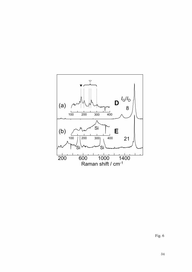
Figure 6 shows representative Raman spectra recorded for Samples D and E. The
presence of SWNTs in Sample D is supported by the appearance of RBMs in the
low-wavenumber region (Fig. 6(a)). Sample E shows an intense peak at around 520
cm-1
originating from the Si-Si lattice vibration of the Si substrate (Fig. 6(b)). A peak at
around 300 cm-1
and another intense peak at around 980 cm-1
detected for Sample E are
assigned to background scattering from the Si substrate. Major RBMs detected for
Samples A-C (Fig. 2) and a specific band featuring VA-SWNTs at around 180 cm-1
(▼)
are also found for Sample D (Fig. 6(a)). The presence of RBMs is not obvious for
Sample E due to the intense background signal at the low wavenumber region (Fig.
6(b)). However, a large G/D-ratio (= 21) and a sharp band shape of the G-band support
the existence of SWNTs.
3.3.2 Field emission properties of SWNTs prepared on textured substrates
In this section, we discuss effects of secondary and tertiary structures on FE
properties. Figure 7 shows the J-E curves and the F-N plots obtained from the first (red)

17
and third (blue) runs for Samples D and E. Figure 8 shows the photographic images of
luminescence from the rear surface of the anode at 3.3, 4.1 and 4.8 V/μm (pulse mode)
for these samples. The FE properties are listed in Table II. Initial protrusions of bundles
in the as-grown samples cause giant field enhancement during the first run. Such
exceptional protrusions may stretch with increasing applied field and finally evaporate.
Compared to for Samples A-C (without texturing), significantly improved FE properties
are revealed for Samples D and E in the subsequent runs (Figs. 7, 8 and Table II). For
the textured Sample, we exclude the possibility of a lowering of φ originating from
amorphous carbon (φ = 1.5 eV)27)
, which can be formed on the tips of pyramids by
current-induced evaporation. To test this assumption, field emission properties of the
textured Si itself (φ = 4.15 eV)28)
and an amorphous carbon film (5 nm) deposited on a
textured Si substrate were evaluated and no emission current was detected from either
samples up to 5.3 V/μm.
In Sample D, protrusive emission sites are located at the edges of VA-SWNTs on
the pyramids (as indicated by arrows in Fig. 5(a), right) since a VA-SWNT film only has
small number of protrusions at the top surface (§3.2.2). A number of straggly SWNTs at
the edges of the film enhance the applied electric field during the subsequent runs.
Moreover in the case that a certain emitter breaks the next emitter becomes active due to

18
the high stacking density of aligned SWNTs. As shown in Fig. 8(a), luminescence is
observed over the whole area. Lowering of field-screening and an extremely high
number of protrusions induce a stable and large area field emission. The inter-pyramid
spacing is 10 – 20 μm, therefore the screening effect is reduced. Pyramid tips with
protrusive bundles selectively become active as emission sites.
Single-bundle emitters with diameters of ca. 10 nm (Fig. 5(b)) and inter-bundle
spacing of 10 – 20 μm in Sample E show the lowest Eto, largest J4.0 (Table II) and the
largest number of luminescent spots (Fig. 8(b)). However the β value for the subsequent
repetitive runs is still comparable with that for Sample D. Single-bundle emitters
entangle or free-stand at the tips of Si pyramids (Fig. 5(b)). These bundles are shorter
than straggled bundles at the edges of the VA-SWNT film in Sample D (Fig. 5(a)).
Screening-free but short bundles in Sample E settles the β as large as that for Sample D.
On the other hand, luminescence image at 3.3 V/μm in Fig. 8(b) shows how the
emission sites disperse in comparison with other samples. Assuming that the number
density of the pyramids in Sample E is approximately 4 × 10⁵ /cm
2 (based on SEM
observation) and field enhancement selectively occurs at the tips of pyramids at 4 V/μm,
the current density of ca. 1 mA/cm2 corresponds to 2.5 nA per pyramid. This gives us a
rough estimate for a tolerable driving current per micro-cathode. Several nA per

19
micro-cathode is a possible design for SWNT-FEDs.
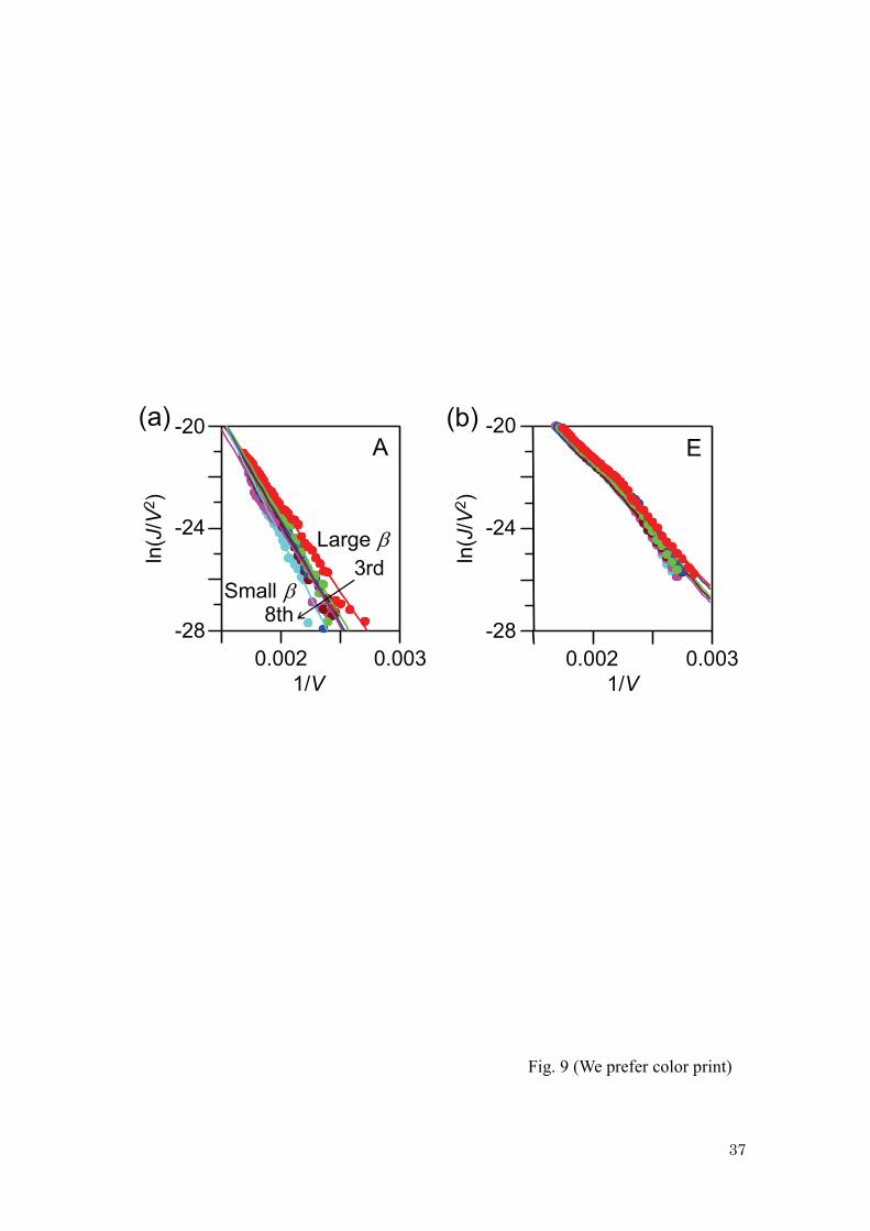
Figure 9 shows linear regressions for the F-N plots obtained from the repetitive
measurements (3rd – 8th runs) for Samples A and E. It is clear that the field
enhancement behavior obtained for Sample E is much more stable in comparison with
Sample A. These results indicate that a well separated tertiary structure and a large tip
curvature of single-bundle protrusions, which fulfill (1) low driving voltage, (2) large
area FE and therefore (3) long life-time, can be prepared though ACCVD by controlling
surface morphologies. In addition, up to now it is revealed that a reaction time of 10 s is
sufficient to prepare SWNT-emitters under ACCVD conditions used in this work.
Consequently morphologically controlled SWNTs prepared through CVD methods have
potential performances for FED applications.
4. Conclusions
SWNT-emitters were prepared on Co/Al2O3(Al)/Si substrates through ACCVD,
which realizes a reaction time of 10 s to grow a 4 μm-thick SWNT film. Field emission
properties of the obtained SWNTs were evaluated under the diode-type configuration.
For a textured Si cathode with SWNT-emitters on Si pyramids, the turn-on electric field
to extract a current density of 1 μA/cm2 was 2.4 V/μm, and a current density of 0.8

20
mA/cm2 was recorded at 4 V/μm. Large area luminescence uniformity (0.5 cm
2) was
also obtained. The study based on the Fowler-Nordheim model showed that field
emission properties of SWNTs are tunable by the morphological control of the
top-surface. Protrusion of emitters is crucial and the optimization of number density,
protrusion length and inter-protrusion distance is necessary for uniform field emission
and increased operating life. Texturing of substrates effects a large and selective field
enhancement at specific protrusive emitters. Currently, SWNTs prepared from ethanol
via a fast and safe process showed field mission characteristics suitable for electron
sources. Controllability of SWNT-growth and morphology is advantageous for further
study on field emission properties.
Acknowledgement
We gratefully thank Mr. Kageyasu Kuroki and Mr. Toshio Ohsawa for technical
supports and Mr. Takao Kishino for phosphor-printing process. The authors sincerely
acknowledge the Ministry of Education, Culture, Sports, Science and Technology
(MEXT), Japan for granting a partial financial support: a Grant-in-Aid for Young
Scientists (A), 1868602, 2006.

21
References
1) A. G. Rinzler, J. H. Hafner, P. Nikolaev, L. Lou, S. G. Kim, D. Tománek, P.
Nordlander, D. T. Colbert, and R. E. Smalley: Science 269 (1995) 1550.
2) J. E. Jung, Y. W. Jin, J. H. Choi, Y. J. Park, T. Y. Ko, D. S. Chung, J. W. Kim, J. E.
Jang, S. N. Cha, W. K. Yi, S. H. Cho, M. J. Yoon, C. G. Lee, J. H. You, N. S. Lee, J. B.
Yoo, and J. M. Kim: Physica B 323 (2002) 71.
3) B. F. Coll, K. A. Dean, E. Howard, S. V. Johnson, M. R. Johnson, H. Li, D. C. Jordan,
L. H. Tisinger, M. Hupp, S. M. Smith, S. R. Young, J. Backer, D. Weston, W. J.
Dauksher, Y. Wei, and J. E. Jaskie: EURODISPLAY ’05, 2005, p. 144.
4) S. Itoh, M. Tanaka, and T. Tonegawa: J. Vac. Sci. Technol. B 22 (2004) 1362.
5) S. Maruyama, R. Kojima, Y. Miyauchi, S. Chiashi, and M. Kohno: Chem. Phys. Lett.
360 (2002) 229.
6) Y. Murakami, S. Chiashi, Y. Miyauchi, M. Hu, M. Ogura, T. Okubo, and S.
Maruyama: Chem. Phys. Lett. 385 (2004) 298.
7) M. Tamura, Y. Kemmochi, Y. Murakami, N. Chino, M. Ogura, S. P. Naik, M. Takai, Y.
Tsuji, S. Maruyama, and T. Okubo: Appl. Phys. A 84 (2006) 247.
8) L. Zhang, L. Balzano, and D. E. Resasco: J. Phys. Chem. B 109 (2005) 14375.
9) S. Noda, Y. Tsuji, Y. Murakami, and S. Maruyama: Appl. Phys. Lett. 86 (2005)

22
173106.
10) S. Noda, H. Sugime, T. Ohsawa, Y. Tsuji, S. Chiashi, Y. Murakami, and S.
Maruyama: Carbon 44 (2006) 1414.
11) M. Sveningsson, R.-E. Morjan, O.A. Nerushev, Y. Sato, J. Bäckström, E.E.B.
Campbell, and F. Rohmund: Appl. Phys. A 73 (2001) 409.
12) S. Noda, K. Hasegawa, H. Sugime, K. Kakehi, Z. Zhang, S. Maruyama, and Y.
Yamaguchi: Jpn. J. Appl. Phys. 46 (2007) L399.
13) L. Zhang, Y. Tan, and D. E. Resasco: Chem. Phys. Lett. 422 (2006) 198.
14) Y. Murakami, S. Chiashi, E. Einarsson, and S. Maruyama: Phys. Rev. B 71 (2005)
085403.
15) K. A. Dean and B. R. Chalamala: Appl. Phys. Lett. 76 (2000) 375.
16) Y. C. Choi, Y. M. Shin, D. J. Bae, S. C. Lim, Y. H. Lee, and B. S. Lee: Diamond
Relat. Mater. 10 (2001) 1457.
17) J.-M. Bonard, C. Klinke, K. A. Dean, and B. F. Coll: Phys. Rev. B 67 (2003)
115406.
18) Y. Saito, K. Seko, and J. Kinoshita: Diamond Relat. Mater. 14 (2005) 1843.
19) Y. Wei, C. Xie, K. A. Dean, and B. F. Coll: Appl. Phys. Lett. 79 (2001) 4527.
20) C. Jin, J. Wang, M. Wang, J. Su, L.-M. Peng: Carbon 43 (2005) 1026.

23
21) H. Sato, K. Hata, H. Miyake, K. Hiramatsu, and Y. Saito: J. Vac. Sci. Technol. B 23
(2005) 754.
22) D. L. Carroll, P. Redlich, P. M. Ajayan, J. C. Charlier, X. Blase, A. De Vita, and R.
Car: Phys. Rev. Lett. 78 (1997) 2811.
23) J.-M. Bonard, J.-P. Salvetat, T. Stöckli, W. A. de Heer, L. Forró, and A. Châtelain:
Appl. Phys. Lett. 73 (1998) 918.
24) W. B. Choi, Y. H. Lee, N. S. Lee, J. H. Kang, S. H. Park, H. Y. Kim, D. S. Chung, S.
M. Lee, S. M. Lee, S. Y. Chung, and J. M. Kim: Jpn. J. Appl. Phys. 39 (2000) 2560.
25) N. S. Xu, Y. Chen, S. Z. Deng, J. Chen, X. C. Ma, and E. G. Wang: J . Phys. D: Appl.
Phys. 34 (2001) 1597.
26) N. S. Xu and S. E. Huq: Mater. Sci. Eng. R 48 (2005) 47.
27) V. M. Anishchik, V. V. Uglov, A. K. Kuleshov, A. R. Filipp, D. P. Rusalsky, M. V.
Astashynskaya, M. P. Samtsov, T. A. Kuznetsova, F. Thiery, and Y. Pauleau: Thin Solid
Films 482 (2005) 248.
28) C. Li, G. Fang, S. Sheng, Z. Chen, J. Wang, S. Ma, and X. Zhao: Physica E 30
(2005) 169.

24
Captions for figures
Fig. 1. SEM micrographs of (a, b) VA-CNTs on the Co/Al2O3/Si (Sample A) and
Co/Al/Si (Sample B) substrates and (c) CNT-grass on the Co/Al/Si substrate (Sample C).
Enlarged image of the top surface of Sample A is shown in (a)-right. Protrusive bundles
in Sample C are indicated by arrows (c).
Fig. 2. Raman spectra of (a, b) VA-CNTs on the Co/Al2O3/Si (Sample A) and Co/Al/Si
(Sample B) substrates and (c) CNT-grass on the Co/Al/Si substrate (Sample C).
Enlarged spectra of the low wavenumber region are indicated in the insets. Major RBMs
are marked by triangles and auxiliary lines: (▼) vertically aligned SWNTs and (∇)
others.
Fig. 3. (a) J-E curves and (b) F-N plots obtained from the first (red) and the third (blue)
measuring runs under the dc-voltage sweep mode for Samples A (○), B (●) and C ( ).
F-N plots for the first runs are composed of two linear relationships with the slopes s1 (<
3 μm) and s2 (> 3 μm). Changes of the slopes observed for Samples A and B at around 3
V/μm during the third run are indicated by an arrow.

25
Fig. 4. Pictures of luminescence from the rear surface of the anode at 3.3, 4.1 and 4.8
V/μm under the pulse driving mode (5 ms, 1/2-duty) and cross-sectional SEM
micrographs; (a) Sample A, (b) Sample B and (c) Sample C.
Fig. 5. SEM micrographs of (a) VA-CNTs on Sample D (left: top view, right: cross
sectional view) and (b) CNT-grass on Sample E (left: entangled bundle, right: vertically
standing bundle) prepared on the textured Co/Al2O3/Si substrates. Protrusions are
indicated by arrows. Inset in (b) is an enlarged image of the bundle.
Fig. 6. Raman spectra of (a) VA-CNTs (Sample D) and (b) CNT-grass (Sample E)
prepared on the textured Co/Al2O3/Si substrates. Enlarged spectra in the low
wavenumber region are indicated in the insets. Major RBMs are marked by triangles
and auxiliary lines: (▼) vertically aligned SWNTs and (∇) others.
Fig. 7. (a) J-E curves and (b) F-N plots obtained from the first (red) and the third (blue)
measuring runs under the dc-voltage sweep mode for Samples D (●) and E (○). F-N
plots for the first runs are composed of two linear relationships with the slopes s1 (< 2
μm) and s2 (> 2 μm).

26
Fig. 8. Pictures of luminescence from the rear surface of the anode at 3.3, 4.1 and 4.8
V/μm under the pulse driving mode (5 ms, 1/2-duty) and cross-sectional SEM
micrographs; (a) Sample D and (b) Sample E. The dark part at the upper left of the
phosphor screen (b) corresponds to a technically generated texture-free area.
Fig. 9. F-N plots obtained from the third to the eighth measuring runs (red: 3rd, green:
4th, blue: 5th, brown: 6th, pink: 7th, light blue: 8th) under the dc-voltage sweep mode
for (a) Sample A and (b) Sample E.

27
Tables
Table I. Conditions of ACCVD on Si substrates at the substrate temperature of 785 °C
and ethanol gas pressure of 4 kPa.
Layer thickness (nm)*1
Sample Morphology
of CNTs Co*2
Al*3
Al2O3*3
Time
(sec)
CNT film
thickness (μm)
G/D-
ratio*5
A VA*6
1.2 ⎯ 10 60 2.7 10
B VA 1.2 7 ⎯ 60 6.0 6
C Grass 1.2 ⎯ 10 60 0.3 14
D VA on Tex.*7
1.2 ⎯ 10 10 4.0 8
E Grass on Tex. 1.2 ⎯ 10 60 0.3 21
*1Average thickness on a flat surface.
*2Catalytic layer.
*3Supporting layer.
*4Data
obtained from Raman spectroscopy presented below. *5
VA: vertically aligned. *6
Tex.:
textured Si substrate.

28
Table II. Turn-on electric fields (Eto), current densities at 4 V/μm (J4.0) and field
enhancement factors (β) obtained for Samples A-E.
Sample Run Eto (Vμm-1
) J4.0 (mAcm-2
) β × 10-5
(cm-1
)
< 3.0 V/μm > 3.0 V/μm 1st 1.9 0.4
2.7 10.4 A
3rd– 2.9 0.2 1.0
< 3.0 V/μm > 3.0 V/μm 1st 2.7 0.5
2.7 10.0 B
3rd – 2.7 0.2 1.3
< 2.5 V/μm > 2.5 V/μm 1st 1.4 0.5
4.5 7.1 C
3rd – 3.1 0.1 0.9
< 1.9 V/μm > 1.9 V/μm 1st 1.4 1.0
3.5 9.1 D
3rd– 2.4 0.6 1.6
< 1.8 V/μm > 1.8 V/μm 1st 1.3 1.2
3.2 8.6 E
3rd– 2.4 0.8 1.4

29
Fig. 1
2 μm
(b) (c)
500 nm
1 μm
(a)
B C
500 nm
A

30
Fig. 2
Raman shift / cm-1200 1000600 1400
6
100 400
10100 400
14100 400
(b)
(a)
(c)
B
A
C
IG/ID

31
Fig. 3 (We prefer color print)
E / V⋅μm-1
J/
A⋅c
m-2
0.002 0.004 0.006
-26
-24
-22
-20
-18
ln(J
/V2)
1/V
S1
S2
(a)
(b)
0 1 2 3 4
10-7
10-8
10-6
10-5
10-4
10-3
10-9

32
Fig. 4 (We prefer color print)
500 nmC
(c)
B
(b)
A
(a)
4.8 V/μm4.1 V/μm3.3 V/μm
2 μm
1 μm
Morphology
7 m
m
8 mm

33
Fig. 5
(a)
5 μm50 μm
D
(b)
500 nm200 nm
E
50 nm
Top view Cross section
5 μm
34
Fig. 6
Raman shift / cm-1200 1000600 1400
8100 400
(a)
200 300
D
21100 400200 300
(b)
IG/ID
E
Si Si
Si

35
Fig. 7 (We prefer color print)
E / V⋅μm-1
J/
A⋅c
m-2
(a)
0.002 0.004 0.006
-26
-24
-22
-20
-18ln
(J/V
2)
1/V
S1
S2
(b)
0 1 2 3 4
10-6
10-7
10-5
10-4
10-3
10-2
10-8
10-9

36
Fig. 8 (We prefer color print)
4.8 V/μm4.1 V/μm3.3 V/μm
D(a)
5 μm
E(b)
500 nm
Morphology
37
Fig. 9 (We prefer color print)
0.002 0.003
-28
-24
-20
ln(J
/V2)
1/V0.002 0.003
-28
-24
-20
ln(J
/V2)
1/V
(a) (b)
3rd
8th
Large β
Small β
A E