Embed Size (px)
Citation preview
als 16 (2007) 74–80www.elsevier.com/locate/diamond
Diamond & Related Materi
Formation of b111N fiber texture in β-SiC filmsdeposited on Si(100) substrates
Velimir Radmilovic a,⁎, Ulrich Dahmen a, Di Gao b, Conrad R. Stoldt b,Carlo Carraro b, Roya Maboudian b
a National Center for Electron Microscopy, Lawrence Berkeley National Laboratory, Berkeley, CA, United Statesb Department of Chemical Engineering, University of California at Berkeley, Berkeley, CA, United States
Received 13 December 2005; received in revised form 28 February 2006; accepted 31 March 2006Available online 9 June 2006
Abstract
The evolution of the morphology and the texture of 3C-SiC films grown by chemical vapor deposition (CVD), using 1,3-disilabutane asprecursor, on Si(100) substrates is investigated by transmission electron microscopy. Films were found to exhibit a columnar grain structure with astrong b111N fiber texture and a high density of stacking faults and twins. The columnar grains do not originate at the substrate surface but on abuffer layer about 3 to 5 nm thick, consisting of interconnected 3D-islands that initiate as epitaxial nuclei. The change from b100N epitaxialislands to b111N columnar grains can be understood in terms of anisotropic growth rates and multiple twinning. The observed b111N fiber texture,faulted substructure, faceted surface morphology and carbon enrichment of the growth surface are in agreement with the proposed growth model.Published by Elsevier B.V.
Keywords: Silicon carbide; Chemical vapor deposition; Nucleation; Twinning; Texture; Intermediate layer; Polar crystal growth model
1. Introduction
Due to its high acoustic velocity and extremely stablephysicochemical properties, silicon carbide has recently beenpursued as a structural material in micro- and nanoelectrome-chanical systems (MEMS and NEMS) for use in harsh envi-ronments [1–3] as well as for ultra-high frequency signalprocessing systems [3,4].
Distinguished from more than 200 polytypes of SiC, a cubicSiC (3C-SiC) film can be obtained by a heteroepitaxial growthon the Si substrates, which offers the possibility of on-chipintegration with Si-based devices. Especially, polycrystalline3C-SiC films can be deposited on a variety of substratesincluding silicon oxide, polycrystalline Si, and silicon nitride,which make fabrication of multilayer MEMS structuresfeasible. As a result, extensive efforts have been directedtoward the growth of polycrystalline 3C-SiC films on Si [5–9].
⁎ Corresponding author.E-mail address: [email protected] (V. Radmilovic).
0925-9635/$ - see front matter. Published by Elsevier B.V.doi:10.1016/j.diamond.2006.03.017
The evolution of the morphology and growth habit of cubicpolar SiC, and non-polar diamond thin films on Si substrates hasbeen studied extensively, both experimentally [10–18] andtheoretically [15–22]. Depending on the substrate temperatureand the environmental conditions, different morphologies, de-fect structures and textures have been observed. However,despite substantial research in this area, the mechanism of low-temperature nucleation and growth of 3C-SiC films with highlytextured columnar grain structures is not yet understood. Theaim of this work is to investigate the mechanism of 3C-SiC filmgrowth on Si(100) substrates and the role of twinning in theformation of the observed strong {111} texture.
2. Experimental procedure
In the present work, the SiC deposition is performed in acustom-built, horizontally oriented hot-wall CVD reactormounted within a stainless steel vacuum chamber. Briefly, thereactor consists of an alumina tube (15 mm inner diameter,150 mm long) with a 50 mm long hot-wall zone, a sample stagewith an integrated thermocouple, and variable leak valves for
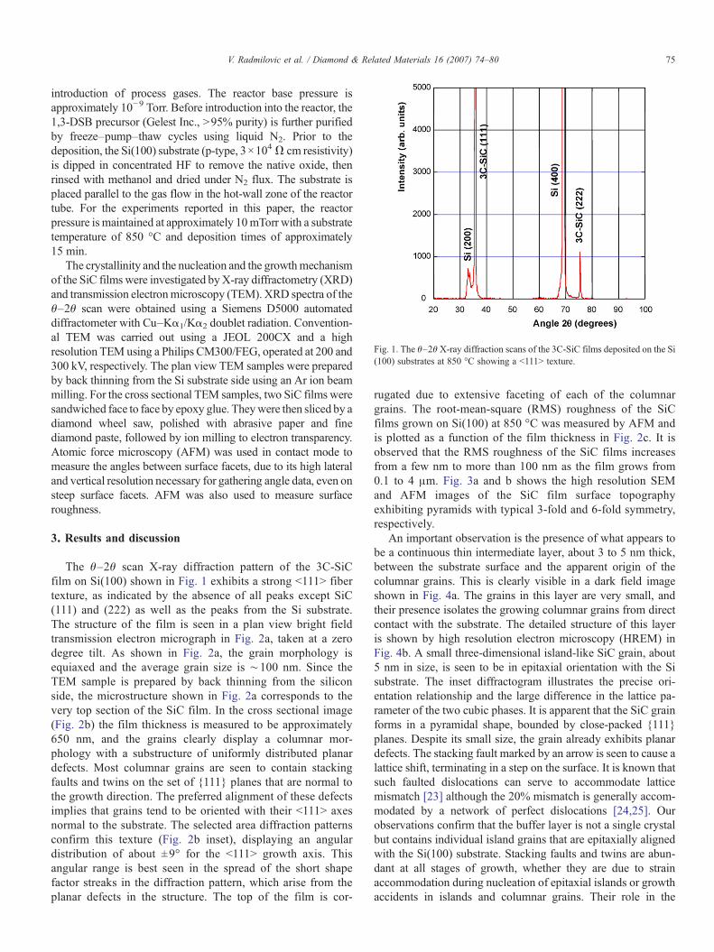
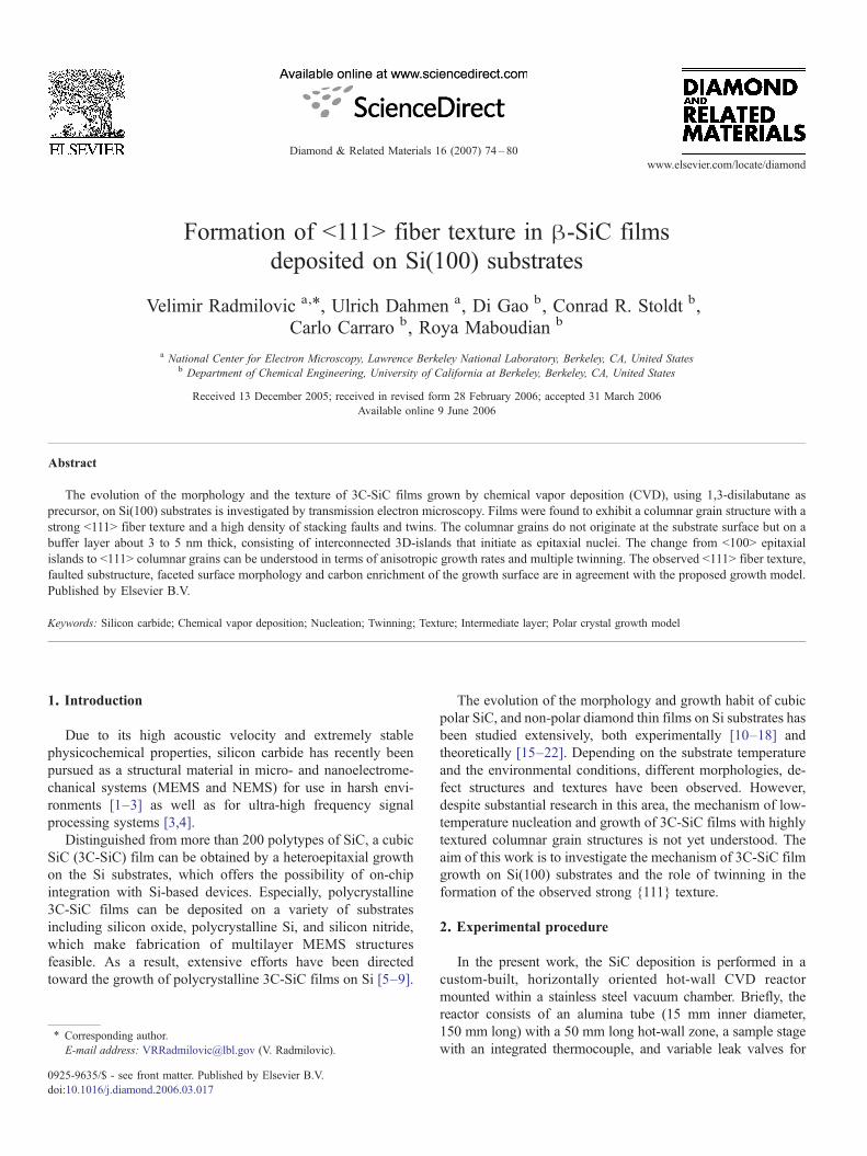
Fig. 1. The θ–2θ X-ray diffraction scans of the 3C-SiC films deposited on the Si(100) substrates at 850 °C showing a b111N texture.
75V. Radmilovic et al. / Diamond & Related Materials 16 (2007) 74–80
introduction of process gases. The reactor base pressure isapproximately 10−9 Torr. Before introduction into the reactor, the1,3-DSB precursor (Gelest Inc., N95% purity) is further purifiedby freeze–pump–thaw cycles using liquid N2. Prior to thedeposition, the Si(100) substrate (p-type, 3×10⁴Ω cm resistivity)is dipped in concentrated HF to remove the native oxide, thenrinsed with methanol and dried under N2 flux. The substrate isplaced parallel to the gas flow in the hot-wall zone of the reactortube. For the experiments reported in this paper, the reactorpressure is maintained at approximately 10mTorr with a substratetemperature of 850 °C and deposition times of approximately15 min.
The crystallinity and the nucleation and the growthmechanismof the SiC films were investigated byX-ray diffractometry (XRD)and transmission electronmicroscopy (TEM). XRD spectra of theθ–2θ scan were obtained using a Siemens D5000 automateddiffractometer with Cu–Kα1/Kα2 doublet radiation. Convention-al TEM was carried out using a JEOL 200CX and a highresolution TEM using a Philips CM300/FEG, operated at 200 and300 kV, respectively. The plan view TEM samples were preparedby back thinning from the Si substrate side using an Ar ion beammilling. For the cross sectional TEM samples, two SiC films weresandwiched face to face by epoxy glue. Theywere then sliced by adiamond wheel saw, polished with abrasive paper and finediamond paste, followed by ion milling to electron transparency.Atomic force microscopy (AFM) was used in contact mode tomeasure the angles between surface facets, due to its high lateraland vertical resolution necessary for gathering angle data, even onsteep surface facets. AFM was also used to measure surfaceroughness.
3. Results and discussion
The θ–2θ scan X-ray diffraction pattern of the 3C-SiCfilm on Si(100) shown in Fig. 1 exhibits a strong b111N fibertexture, as indicated by the absence of all peaks except SiC(111) and (222) as well as the peaks from the Si substrate.The structure of the film is seen in a plan view bright fieldtransmission electron micrograph in Fig. 2a, taken at a zerodegree tilt. As shown in Fig. 2a, the grain morphology isequiaxed and the average grain size is ∼100 nm. Since theTEM sample is prepared by back thinning from the siliconside, the microstructure shown in Fig. 2a corresponds to thevery top section of the SiC film. In the cross sectional image(Fig. 2b) the film thickness is measured to be approximately650 nm, and the grains clearly display a columnar mor-phology with a substructure of uniformly distributed planardefects. Most columnar grains are seen to contain stackingfaults and twins on the set of {111} planes that are normal tothe growth direction. The preferred alignment of these defectsimplies that grains tend to be oriented with their b111N axesnormal to the substrate. The selected area diffraction patternsconfirm this texture (Fig. 2b inset), displaying an angulardistribution of about ±9° for the b111N growth axis. Thisangular range is best seen in the spread of the short shapefactor streaks in the diffraction pattern, which arise from theplanar defects in the structure. The top of the film is cor-
rugated due to extensive faceting of each of the columnargrains. The root-mean-square (RMS) roughness of the SiCfilms grown on Si(100) at 850 °C was measured by AFM andis plotted as a function of the film thickness in Fig. 2c. It isobserved that the RMS roughness of the SiC films increasesfrom a few nm to more than 100 nm as the film grows from0.1 to 4 μm. Fig. 3a and b shows the high resolution SEMand AFM images of the SiC film surface topographyexhibiting pyramids with typical 3-fold and 6-fold symmetry,respectively.
An important observation is the presence of what appears tobe a continuous thin intermediate layer, about 3 to 5 nm thick,between the substrate surface and the apparent origin of thecolumnar grains. This is clearly visible in a dark field imageshown in Fig. 4a. The grains in this layer are very small, andtheir presence isolates the growing columnar grains from directcontact with the substrate. The detailed structure of this layeris shown by high resolution electron microscopy (HREM) inFig. 4b. A small three-dimensional island-like SiC grain, about5 nm in size, is seen to be in epitaxial orientation with the Sisubstrate. The inset diffractogram illustrates the precise ori-entation relationship and the large difference in the lattice pa-rameter of the two cubic phases. It is apparent that the SiC grainforms in a pyramidal shape, bounded by close-packed {111}planes. Despite its small size, the grain already exhibits planardefects. The stacking fault marked by an arrow is seen to cause alattice shift, terminating in a step on the surface. It is known thatsuch faulted dislocations can serve to accommodate latticemismatch [23] although the 20% mismatch is generally accom-modated by a network of perfect dislocations [24,25]. Ourobservations confirm that the buffer layer is not a single crystalbut contains individual island grains that are epitaxially alignedwith the Si(100) substrate. Stacking faults and twins are abun-dant at all stages of growth, whether they are due to strainaccommodation during nucleation of epitaxial islands or growthaccidents in islands and columnar grains. Their role in the
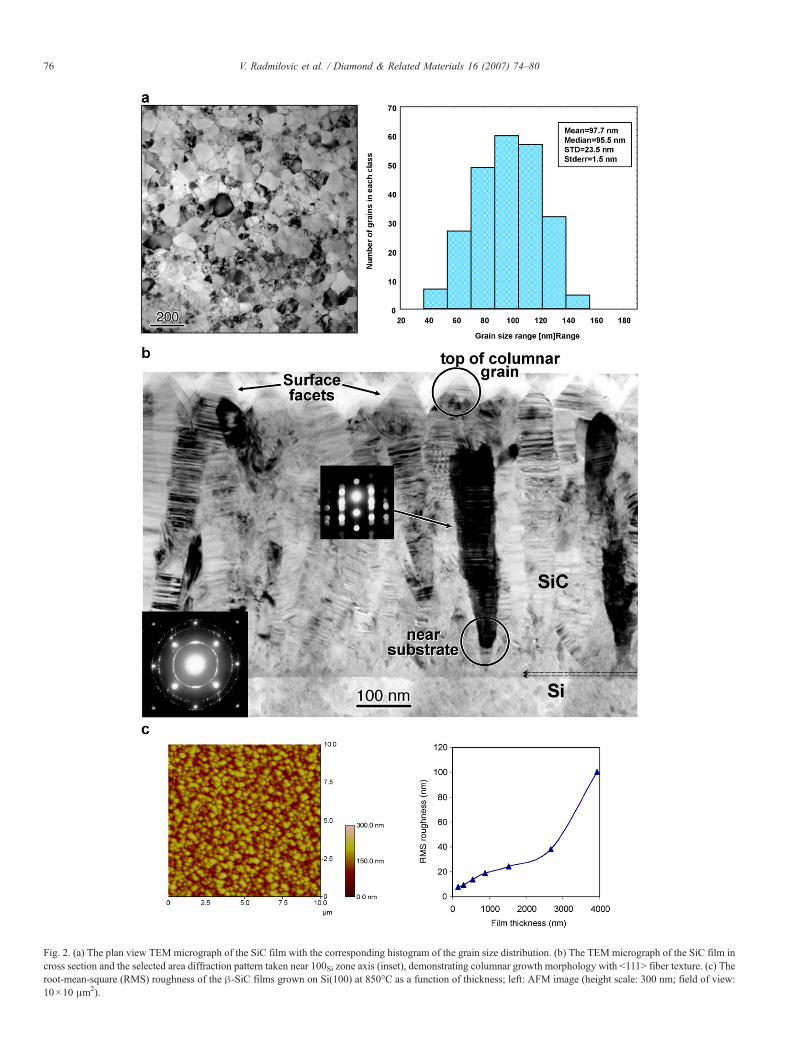
Fig. 2. (a) The plan view TEMmicrograph of the SiC film with the corresponding histogram of the grain size distribution. (b) The TEM micrograph of the SiC film incross section and the selected area diffraction pattern taken near 100Si zone axis (inset), demonstrating columnar growth morphology with b111N fiber texture. (c) Theroot-mean-square (RMS) roughness of the β-SiC films grown on Si(100) at 850°C as a function of thickness; left: AFM image (height scale: 300 nm; field of view:10×10 μm2).
76 V. Radmilovic et al. / Diamond & Related Materials 16 (2007) 74–80
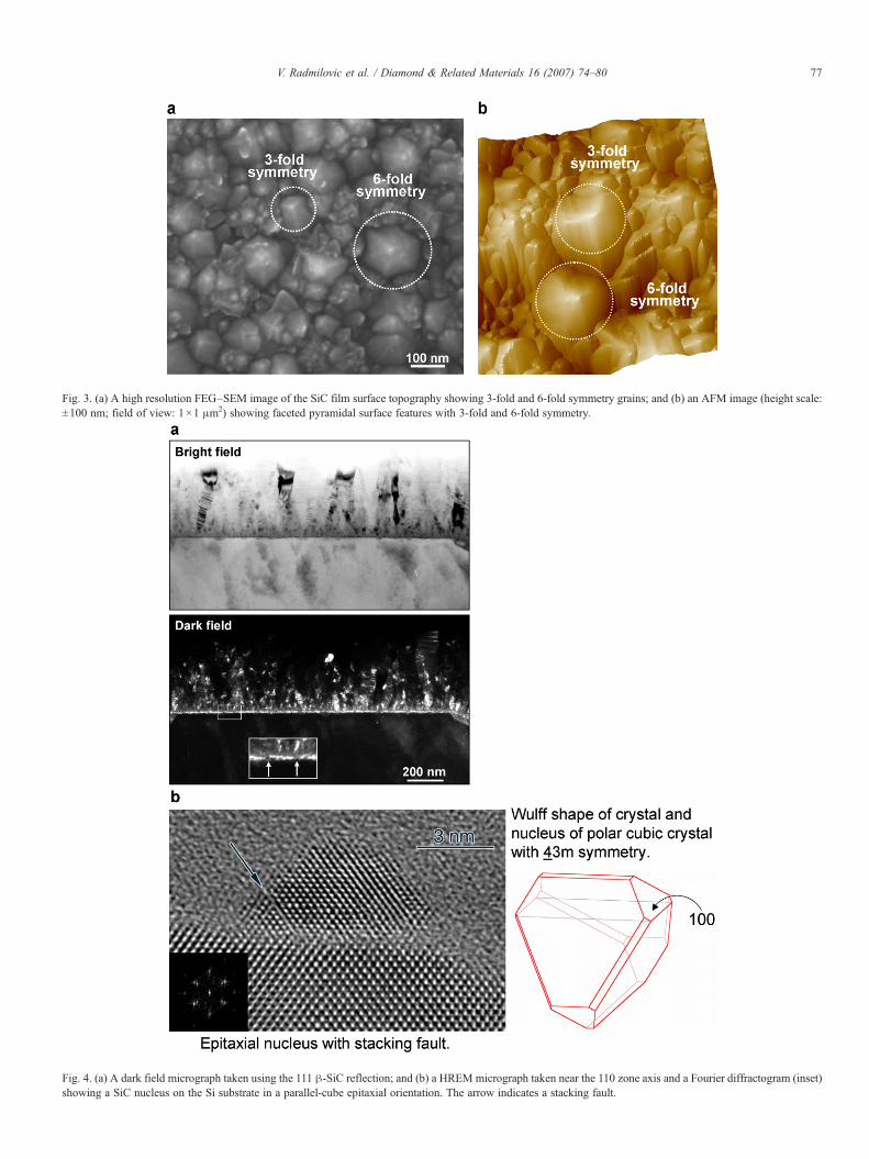
Fig. 3. (a) A high resolution FEG–SEM image of the SiC film surface topography showing 3-fold and 6-fold symmetry grains; and (b) an AFM image (height scale:±100 nm; field of view: 1×1 μm2) showing faceted pyramidal surface features with 3-fold and 6-fold symmetry.
Fig. 4. (a) A dark field micrograph taken using the 111 β-SiC reflection; and (b) a HREM micrograph taken near the 110 zone axis and a Fourier diffractogram (inset)showing a SiC nucleus on the Si substrate in a parallel-cube epitaxial orientation. The arrow indicates a stacking fault.
77V. Radmilovic et al. / Diamond & Related Materials 16 (2007) 74–80
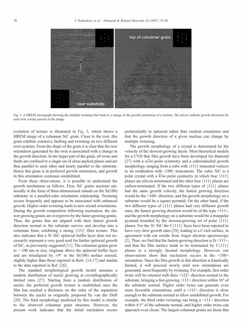
Fig. 5. A HREM micrograph showing the multiple twinning that leads to a change in the growth orientation of a nucleus. The arrows indicate growth directions foreach twin variant present in the image.
78 V. Radmilovic et al. / Diamond & Related Materials 16 (2007) 74–80
evolution of texture is illustrated in Fig. 5, which shows aHREM image of a columnar SiC grain. Close to the root, thisgrain exhibits extensive faulting and twinning on two differenttwin systems. From the shape of the grain it is clear that the neworientation generated by the twin is associated with a change inthe growth direction. In the larger part of the grain, all twins andfaults are confined to a single set of close-packed planes and arethus parallel to each other and nearly parallel to the substrate.Hence this grain is in preferred growth orientation, and growthin this orientation continues uninhibited.
From these observations, it is possible to understand thegrowth mechanism as follows. First, SiC grains nucleate epi-taxially in the form of three-dimensional islands on the Si(100)substrate in a parallel-cube orientation relationship. Twinningoccurs frequently and appears to be associated with enhancedgrowth. Higher order twinning leads to new crystal orientations.During the growth competition following nucleation, the slo-wer-growing grains are overgrown by the faster-growing grains.Thus, the grains that are aligned with their fastest growthdirection normal to the substrate survive and develop into acolumnar form, exhibiting a strong {111} fiber texture. Thisalso indicates that a 3C-SiC epitaxial buffer layer does not ne-cessarily represent a very good seed for further epitaxial growthof SiC, as previously suggested [11]. The columnar grains growto ∼100 nm in size, originate above the epitaxial buffer layerand are misaligned by ±9° to the Si(100) surface normal,slightly higher than those reported in Refs. [14,17] and similarto the data reported in Ref. [26].
The standard morphological growth model assumes arandom distribution of nuclei growing at crystallographicallylimited rates [27]. Starting from a random distribution ofnuclei, the preferred growth texture is established once thefilm has reached a thickness on the order of the separationbetween the nuclei as originally proposed by van der Drift[28]. The final morphology predicted by this model is similarto the observed columnar grain structure. However, thepresent work indicates that the initial nucleation occurs
preferentially in epitaxial rather than random orientation andthat the growth direction of a given nucleus can change bymultiple twinning.
The growth morphology of a crystal is determined by thevelocity of the slowest-growing facets. Most theoretical modelsfor a CVD thin film growth have been developed for diamond[27] with a m3̄m point symmetry and a cuboctahedral growthmorphology, ranging from a cube with {111}-truncated verticesto an octahedron with {100} truncations. The cubic SiC is apolar crystal with a 4̄3m point symmetry in which four {111}planes are silicon-terminated and the other four {111} planes arecarbon-terminated. If the two different types of {111} planeshad the same growth velocity, the fastest growing directionwould be the b100N direction, and the growth morphology on asubstrate would be a square pyramid. On the other hand, if thetwo different types of {111} planes had very different growthrates, the fastest growing direction would be of the type b111N,and the growth morphology on a substrate would be a triangularpyramid bounded by the slowest-growing set of polar {111}planes. For the 3C-SiC the C{111} faces have been reported tohave very slow growth rates [29], leading to a C-rich surface, inagreement with our results from Auger electron spectroscopy[2]. Thus, we find that the fastest-growing direction is Si b111N,and that the film surface tends to be terminated by C{111}planes in a strongly faceted morphology. However, ourobservations show that nucleation occurs in the b100Norientation. Since the film growth in this direction is kineticallylimited, it will proceed slowly until new orientations aregenerated, most frequently by twinning. For example, first ordertwins will be oriented with their b122N direction normal to thesubstrate, bringing a fast-growing b111N direction within 16° ofthe substrate normal. Higher order twins can generate evenmore favorable orientations, until a b111N direction is closeenough to the substrate normal to allow uninhibited growth. Forexample, the third order twinning can bring a b111N directionwithin 8.5° of the substrate normal, and higher order twins canapproach even closer. The largest columnar grains are those that
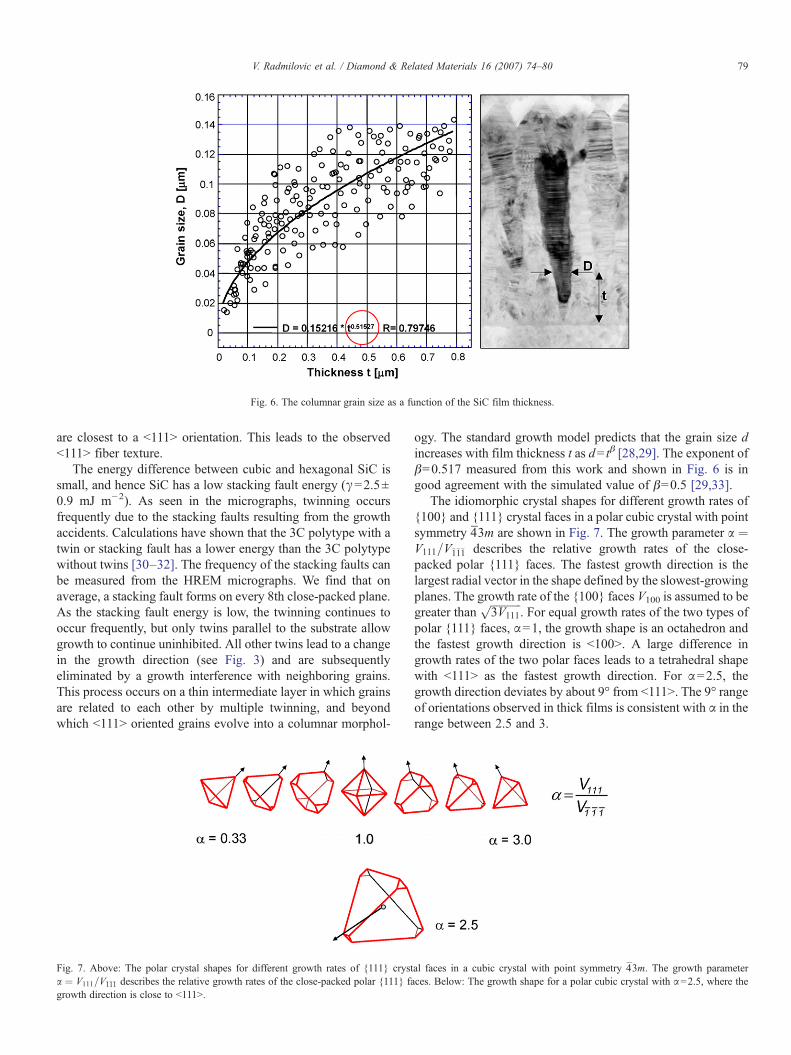
Fig. 6. The columnar grain size as a function of the SiC film thickness.
79V. Radmilovic et al. / Diamond & Related Materials 16 (2007) 74–80
are closest to a b111N orientation. This leads to the observedb111N fiber texture.
The energy difference between cubic and hexagonal SiC issmall, and hence SiC has a low stacking fault energy (γ=2.5±0.9 mJ m−2). As seen in the micrographs, twinning occursfrequently due to the stacking faults resulting from the growthaccidents. Calculations have shown that the 3C polytype with atwin or stacking fault has a lower energy than the 3C polytypewithout twins [30–32]. The frequency of the stacking faults canbe measured from the HREM micrographs. We find that onaverage, a stacking fault forms on every 8th close-packed plane.As the stacking fault energy is low, the twinning continues tooccur frequently, but only twins parallel to the substrate allowgrowth to continue uninhibited. All other twins lead to a changein the growth direction (see Fig. 3) and are subsequentlyeliminated by a growth interference with neighboring grains.This process occurs on a thin intermediate layer in which grainsare related to each other by multiple twinning, and beyondwhich b111N oriented grains evolve into a columnar morphol-
Fig. 7. Above: The polar crystal shapes for different growth rates of {111} crysta ¼ V111=V1̄1̄1̄ describes the relative growth rates of the close-packed polar {111} fagrowth direction is close to b111N.
ogy. The standard growth model predicts that the grain size dincreases with film thickness t as d= tβ [28,29]. The exponent ofβ=0.517 measured from this work and shown in Fig. 6 is ingood agreement with the simulated value of β=0.5 [29,33].
The idiomorphic crystal shapes for different growth rates of{100} and {111} crystal faces in a polar cubic crystal with pointsymmetry 4̄3m are shown in Fig. 7. The growth parameter a ¼V111=V1̄1̄1̄ describes the relative growth rates of the close-packed polar {111} faces. The fastest growth direction is thelargest radial vector in the shape defined by the slowest-growingplanes. The growth rate of the {100} faces V100 is assumed to begreater than
ffiffiffiffiffiffiffiffiffiffiffi
3V111p
. For equal growth rates of the two types ofpolar {111} faces, α=1, the growth shape is an octahedron andthe fastest growth direction is b100N. A large difference ingrowth rates of the two polar faces leads to a tetrahedral shapewith b111N as the fastest growth direction. For α=2.5, thegrowth direction deviates by about 9° from b111N. The 9° rangeof orientations observed in thick films is consistent with α in therange between 2.5 and 3.
al faces in a cubic crystal with point symmetry 4̄3m. The growth parameterces. Below: The growth shape for a polar cubic crystal with α=2.5, where the
80 V. Radmilovic et al. / Diamond & Related Materials 16 (2007) 74–80
4. Conclusion
In conclusion, the evolution of the thin film morphology andthe growth habits of the polycrystalline 3C-SiC on Si(100)substrates during a low-temperature CVD growth have beenstudied by transmission electron microscopy. The HREM re-veals that nucleation occurs in epitaxial 3-D pyramid-likemicrocrystals bounded by slow-growing C{111} planes. Thelow stacking fault energy leads to frequent twinning, and mul-tiple twinning changes the crystal orientation during growth.The growth competition leads to the termination of the slow-growing orientations, causing a transition from b100N orientedepitaxial islands to b111N oriented columnar SiC grains. Thisprocess results in a columnar grain structure separated from thesubstrate by a ∼5 nm transition layer that accommodates theorientation change via multiple twinning. The observed b111Nfiber texture, faulted substructure, faceted surface morphologyand carbon enrichment of the growth surface are in agreementwith this growth model for polar crystals.
Acknowledgements
This work is supported by the Director, Office of Science,Office of Basic Energy Sciences, Materials Sciences andEngineering Division of the U.S. Department of Energy underContract No. DE-AC02-05CH1123.
References
[1] M. Mehregany, et al., Int. Mater. Rev. 45 (2000) 85.[2] C.R. Stoldt, et al., Sens. Actuators, A, Phys. 97–98 (2002) 410.[3] Y.T. Yang, K.L. Ekinci, X.M.H. Huang, L.M. Schiavone,M.L. Roukes, C.A.
Zorman, M. Mehregany, Appl. Phys. Lett. 78 (2001) 162.[4] X.M.H. Huang, C.A. Zorman, M. Mehregany, M.L. Roukes, Nature 421
(2003) 496.[5] C.A. Zorman, A.J. Fleischman, A.S. Dewa, M. Mehregany, C. Jacob, S.
Nishino, P. Pirouz, J. Appl. Phys. 78 (1995) 5136.
[6] M. Mehregany, C.A. Zorman, Thin Solid Films 355–356 (1999) 518.[7] K. Nishino, J.A. Powell, H.A. Will, Appl. Phys. Lett. 42 (1983) 460.[8] T. Yoshinobu, H. Mitsui, Y. Tarui, T. Fuyuki, H. Matsunami, J. Appl. Phys.
72 (1992) 2006.[9] M. Kitabatake, M. Deguchi, T. Hirao, J. Appl. Phys. 74 (1993) 4438.[10] Y.H. Seo, K.S. Nahm, E.-K. Suh, H.J. Lee, Y.G. Hwang, J. Vac. Sci.
Technol., A 15 (1997) 2226.[11] G. Ferro, Y. Monteli, H. Vincent, V. Thevenot, M.D. Tran, F. Cauwet,
J. Bouix, J. Appl. Phys. 80 (1996) 4691.[12] C. Bittencourt, Surf. Interface Anal. 30 (2000) 603.[13] M.W. Russell, J.A. Freitas, W.J. Moore, J.E. Butler, Adv. Mater. Opt.
Electron. 7 (1997) 195.[14] J. Krausslich, A. Fissel, U. Kaiser, K. Goetz, L. Dressler, J. Phys., D-Appl.
Phys. 28 (1995) 759.[15] C. Wild, N. Herres, P. Koidl, J. Appl. Phys. 68 (1990) 973.[16] C. Wild, P. Koidl, W. Muller-Sebert, H. Walcher, R. Khol, N. Herres, R.
Locher, Diamond Relat. Mater. 2 (1993) 158.[17] L.O. Bjorketun, L. Hultman, I.P. Ivanov, Q.Wahab, J.E. Sundgren, J. Cryst.
Growth 182 (1997) 379.[18] J.H. Boo,D.C. Lim, S.B. Lee,K.W. Lee,M.M. Sung,Y.Kim,K.S.Yu, J. Vac.
Sci. Technol., B 21 (2003) 1870.[19] J. Yun, D.S. Dandy, Diamond Relat. Mater. 9 (2000) 439.[20] M. Kitabatake, Thin Solid Films 369 (2000) 257.[21] J. Yun, D.S. Dandy, Diamond Relat. Mater. 9 (2000) 439.[22] G. Carter, Vacuum 56 (2000) 87.[23] F. Ernst, P. Pirouz, J. Mater. Res. 4 (1989) 834.[24] C. Long, S.A. Ustin, W. Ho, J. Appl. Phys. 86 (1999) 2509.[25] G. Cicero, L. Pizzagalli, A. Catellani, Phys. Rev. Lett. 89 (2002) 156101.[26] C. Wild, R. Khol, N. Herres, W. Muller-Sebert, P. Koidl, Diamond Relat.
Mater. 2 (1993) 158.[27] J.P. Li, A.J. Steckl, I. Golecki, F. Reidinger, L. Wang, X.J. Ning, P. Pirouz,
Appl. Phys. Lett. 62 (1993) 3135.[28] A. van der Drift, Philips Res. Rep. 22 (1967) 267.[29] F. Paritosh, D.J. Srolovitz, C.C. Battaile, J.E. Butler, Acta Mater. 47 (1999)
2269.[30] L. Wang, W. Wada, L.F. Allard, J. Mater. Res. 7 (1992) 148.[31] C. Cheng, R.J. Needs, V. Heine, J. Phys. C. Solid State Phys. 21 (1988) 1049.[32] P.J.H. Denteneer, in: J. Tersoff, D. Vanderbilt, V. Vitek (Eds.), Atomic
Scale Calculation in Materials Science, MRS Proceed, vol. 141, 1989,p. 343.
[33] P. Smereka, X. Li, G. Russo, D.J. Srolowitz, Acta Mater. 53 (2005) 1191.