Embed Size (px)
Citation preview
1
Introduction to Biomedical Engineering
Kung-Bin Sung5/28/2007
Biomedical Instrumentation
2
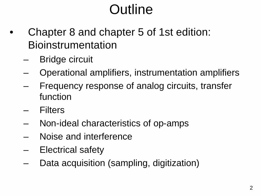
Outline
• Chapter 8 and chapter 5 of 1st edition: Bioinstrumentation
– Bridge circuit– Operational amplifiers, instrumentation amplifiers– Frequency response of analog circuits, transfer
function– Filters– Non-ideal characteristics of op-amps– Noise and interference– Electrical safety– Data acquisition (sampling, digitization)
3
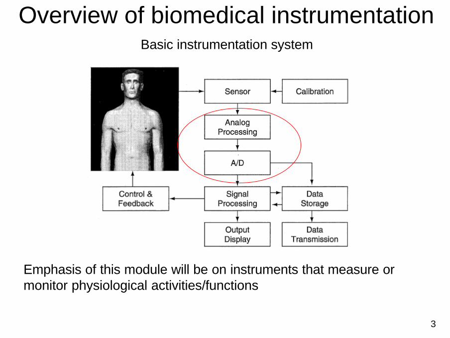
Overview of biomedical instrumentation
Emphasis of this module will be on instruments that measure or monitor physiological activities/functions
Basic instrumentation system
4
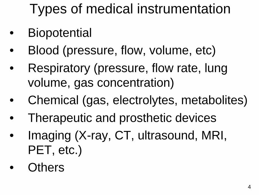
Types of medical instrumentation
• Biopotential• Blood (pressure, flow, volume, etc)• Respiratory (pressure, flow rate, lung
volume, gas concentration)• Chemical (gas, electrolytes, metabolites)• Therapeutic and prosthetic devices• Imaging (X-ray, CT, ultrasound, MRI,
PET, etc.)• Others
5
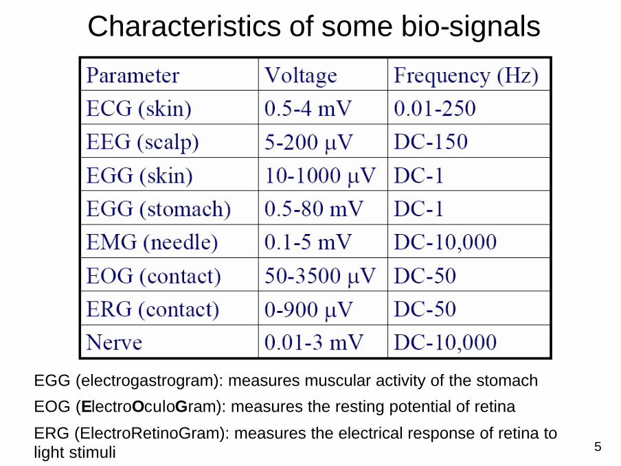
Characteristics of some bio-signals
EOG (ElectroOculoGram): measures the resting potential of retina
ERG (ElectroRetinoGram): measures the electrical response of retina to light stimuli
EGG (electrogastrogram): measures muscular activity of the stomach
6
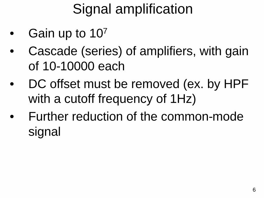
Signal amplification
• Gain up to 107
• Cascade (series) of amplifiers, with gain of 10-10000 each
• DC offset must be removed (ex. by HPF with a cutoff frequency of 1Hz)
• Further reduction of the common-mode signal
7
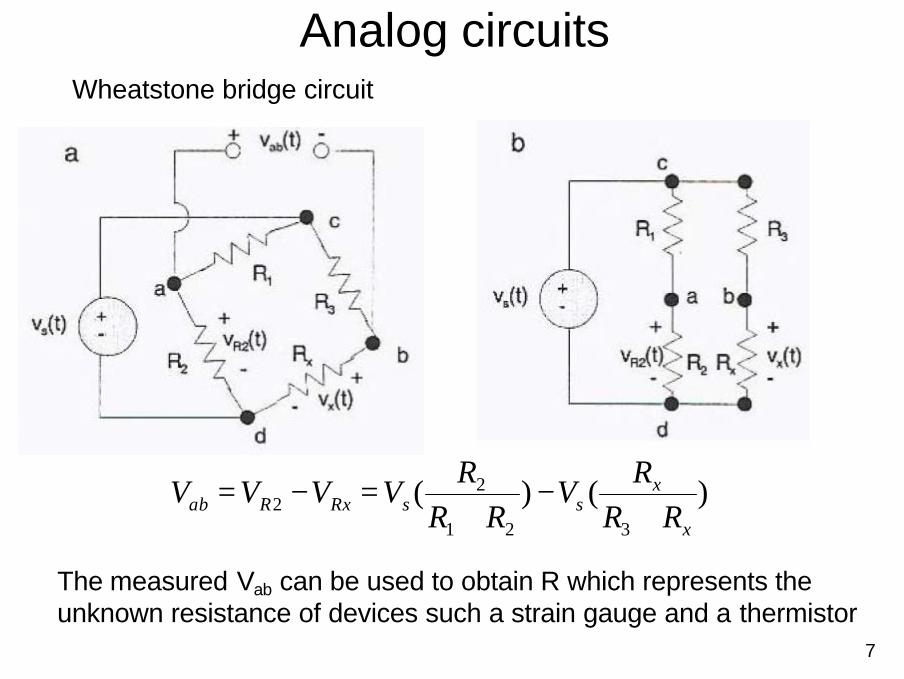
Analog circuitsWheatstone bridge circuit
)()(321
22
x
xssRxRab RR
RV
RRR
VVVV+
−+
=−=
The measured Vab can be used to obtain R which represents the unknown resistance of devices such a strain gauge and a thermistor
8
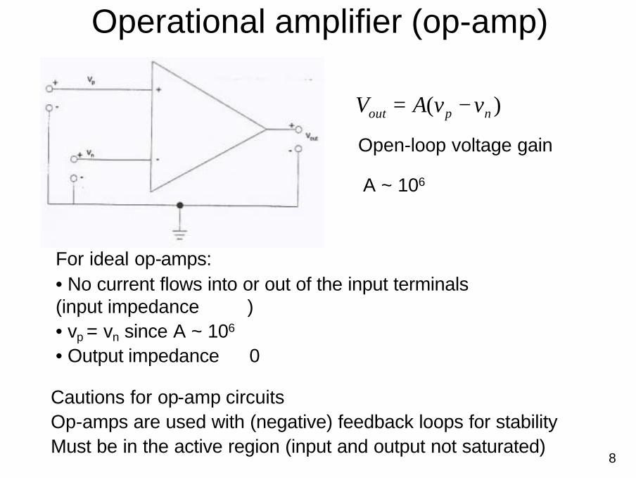
Operational amplifier (op-amp)
)( npout vvAV −=
A ~ 106
For ideal op-amps: •No current flows into or out of the input terminals (input impedance →∞)•vp = vn since A ~ 106
•Output impedance → 0
Open-loop voltage gain
Cautions for op-amp circuitsOp-amps are used with (negative) feedback loops for stabilityMust be in the active region (input and output not saturated)
9
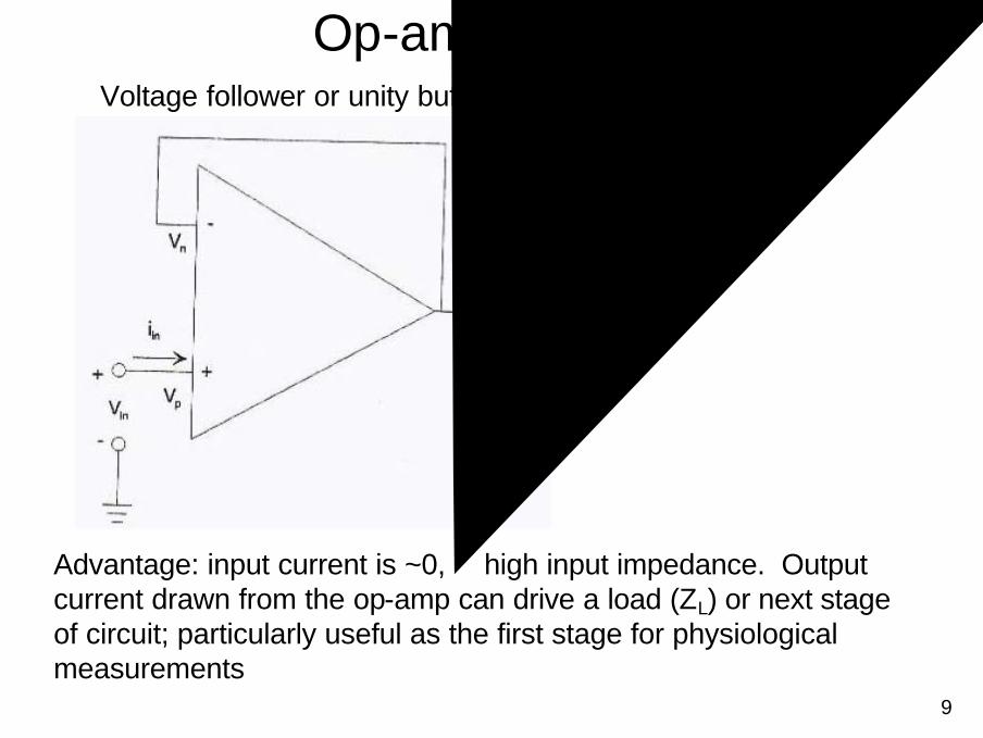
Op-amp circuitsVoltage follower or unity buffer
Vout = Vin
G=1
Advantage: input current is ~0, ∵high input impedance. Output current drawn from the op-amp can drive a load (ZL) or next stage of circuit; particularly useful as the first stage for physiological measurements
10
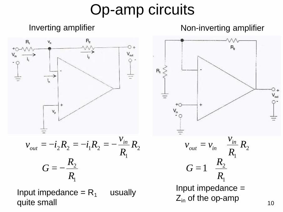
Op-amp circuits
21
2122 RRv
RiRiv inout −=−=−=
1
2
RR
G −=
Input impedance = R1 ⇒ usually quite small
Inverting amplifier Non-inverting amplifier
21
RRv
vv ininout +=
1
21RR
G +=
Input impedance =Zin of the op-amp
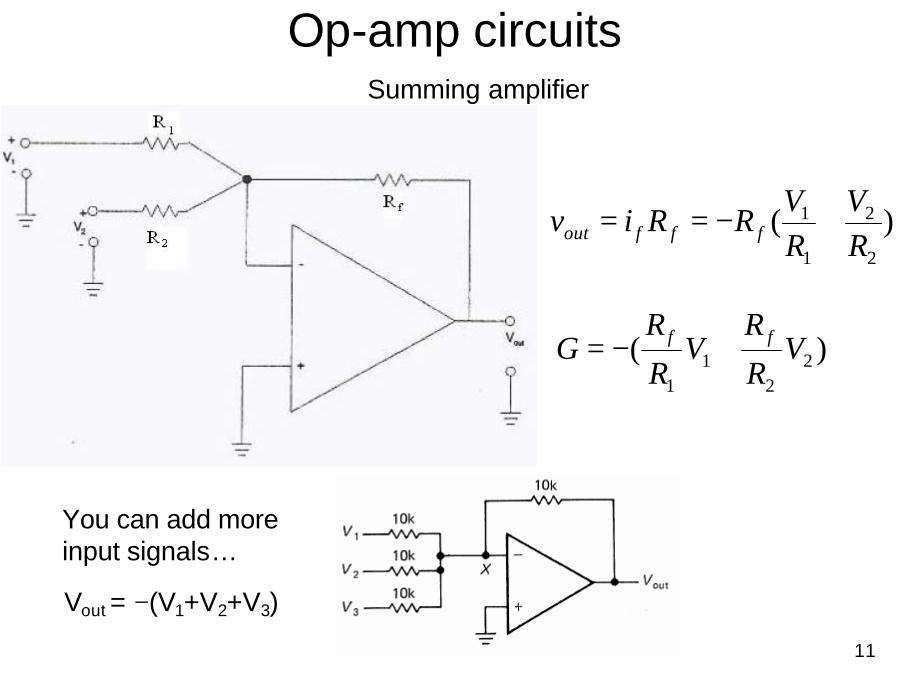
11
Op-amp circuits
)(2
2
1
1
RV
RV
RRiv fffout +−==
)( 22
11
VR
RV
R
RG ff +−=
Summing amplifier
You can add more input signals…
Vout = −(V1+V2+V3)
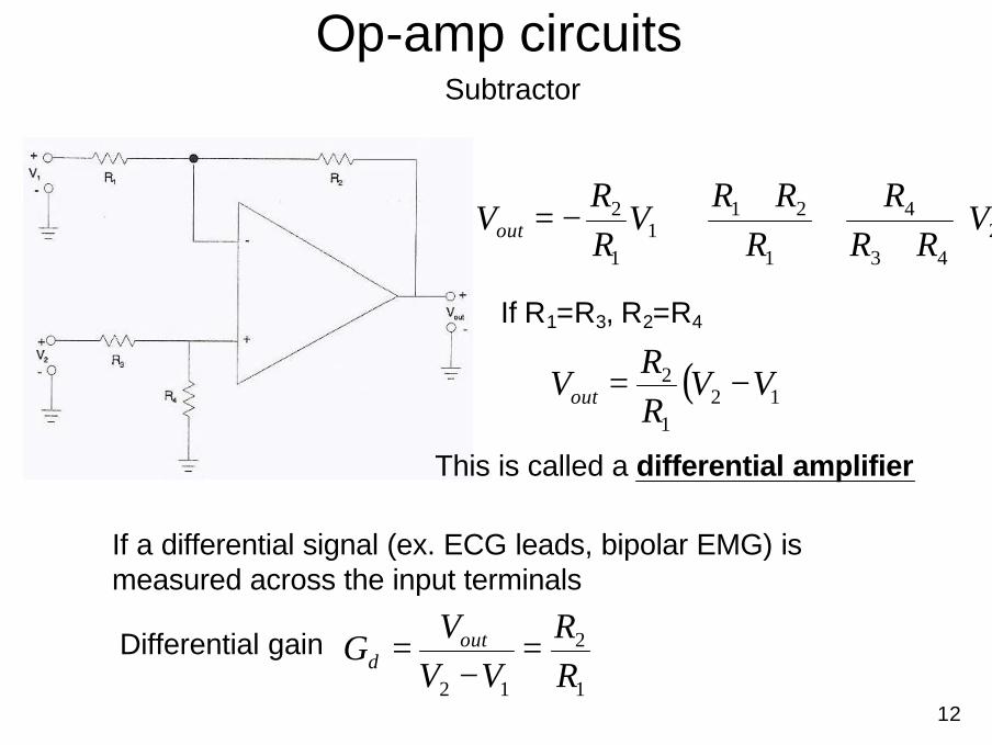
12
Op-amp circuits
243
4
1
211
1
2 VRR
RR
RRV
RR
Vout
+
++−=
( )121
2 VVRR
Vout −=
Subtractor
If R1=R3, R2=R4
This is called a differential amplifier
If a differential signal (ex. ECG leads, bipolar EMG) is measured across the input terminals
1
2
12 RR
VVV
G outd =
−=Differential gain
13
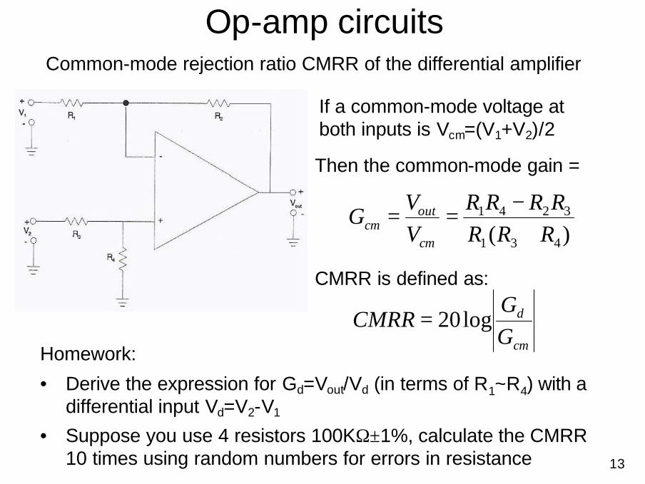
Op-amp circuits
)( 431
3241
RRRRRRR
VV
Gcm
outcm +
−==
Then the common-mode gain =
Homework:
• Derive the expression for Gd=Vout/Vd (in terms of R1~R4) with a differential input Vd=V2-V1
• Suppose you use 4 resistors 100KΩ±1%, calculate the CMRR 10 times using random numbers for errors in resistance
Common-mode rejection ratio CMRR of the differential amplifier
If a common-mode voltage at both inputs is Vcm=(V1+V2)/2
cm
d
GG
CMRR log20=
CMRR is defined as:
14
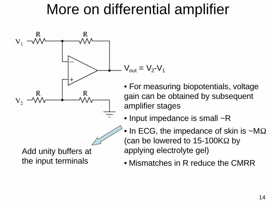
More on differential amplifier
Vout = V2-V1
•For measuring biopotentials, voltage gain can be obtained by subsequent amplifier stages
• Input impedance is small ~R
• In ECG, the impedance of skin is ~MΩ(can be lowered to 15-100KΩ by applying electrolyte gel)
•Mismatches in R reduce the CMRRAdd unity buffers at the input terminals
15
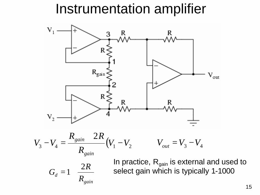
Instrumentation amplifier
( )2143
2VV
R
RRVV
gain
gain −+
=−
gaind R
RG
21+=
43 VVVout −=
In practice, Rgain is external and used to select gain which is typically 1-1000
16
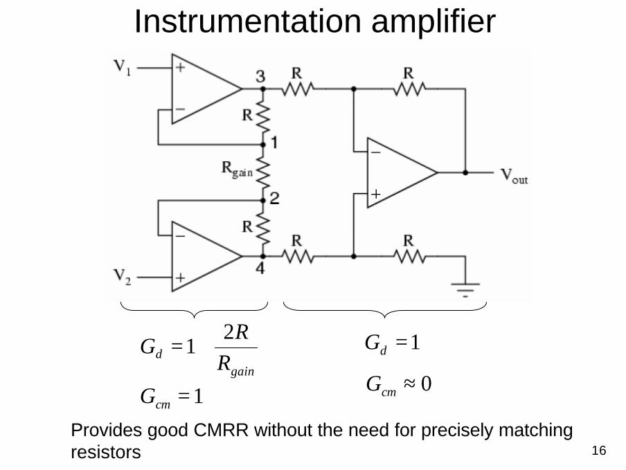
Instrumentation amplifier
1=cmG
1=dGgain
d RR
G2
1+=
0≈cmG
Provides good CMRR without the need for precisely matching resistors
17
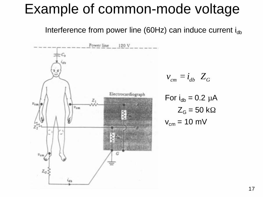
Example of common-mode voltageInterference from power line (60Hz) can induce current idb
Gdbcm Ziv ⋅=
For idb = 0.2 µA
ZG = 50 kΩvcm = 10 mV
18
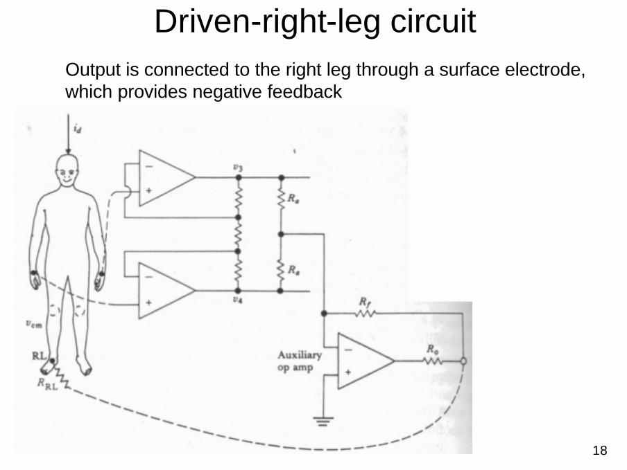
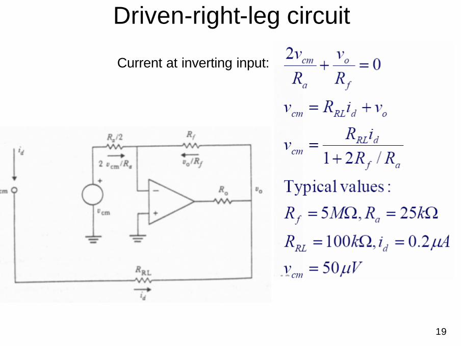
Driven-right-leg circuitOutput is connected to the right leg through a surface electrode, which provides negative feedback
19
Driven-right-leg circuit
Current at inverting input:
20
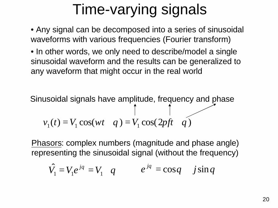
Time-varying signals
)2cos()cos()( 111 θπθω +=+= ftVtVtv
θθ ∠== 111 VeVV j θθθ sincos je j +=
Sinusoidal signals have amplitude, frequency and phase
Phasors: complex numbers (magnitude and phase angle) representing the sinusoidal signal (without the frequency)
•Any signal can be decomposed into a series of sinusoidal waveforms with various frequencies (Fourier transform)• In other words, we only need to describe/model a single sinusoidal waveform and the results can be generalized to any waveform that might occur in the real world
21
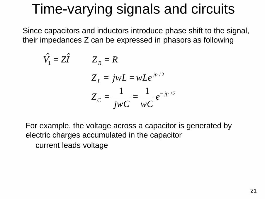
Time-varying signals and circuits
IZV ˆ1 = RZ R =
2/πωω jL LeLjZ ==
2/11 π
ωωj
C eCCj
Z −==
Since capacitors and inductors introduce phase shift to the signal, their impedances Z can be expressed in phasors as following
For example, the voltage across a capacitor is generated by electric charges accumulated in the capacitor∴ current leads voltage
22
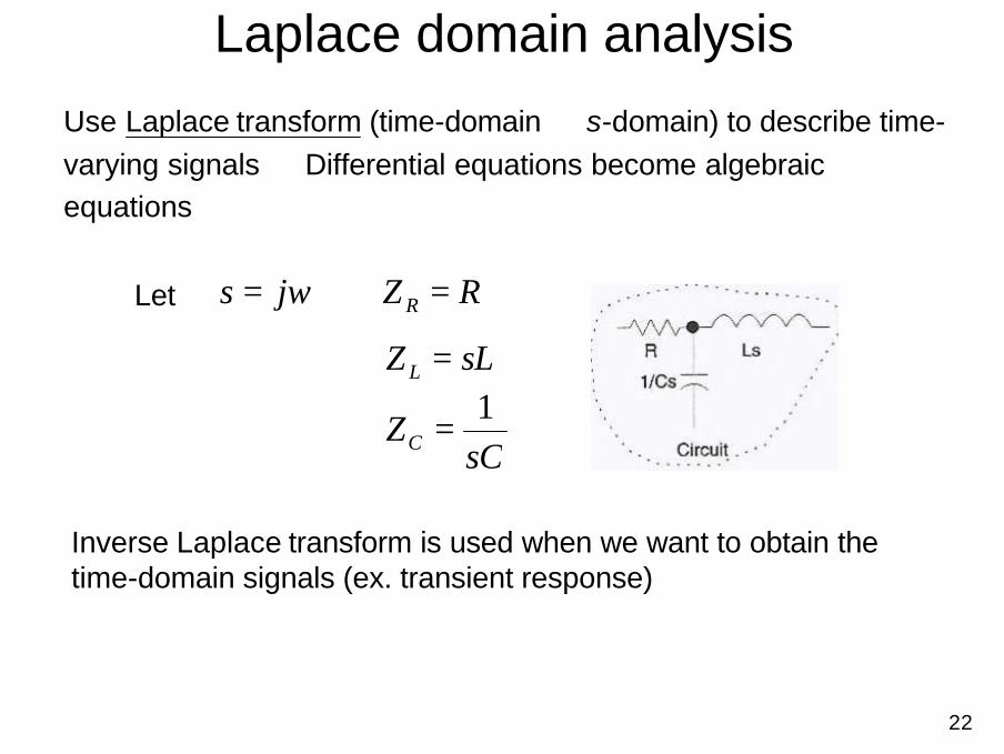
Laplace domain analysis
ωjs = RZ R =
sLZ L =
sCZC
1=
Use Laplace transform (time-domain → s-domain) to describe time-varying signals ⇒ Differential equations become algebraicequations
Let
Inverse Laplace transform is used when we want to obtain the time-domain signals (ex. transient response)
23
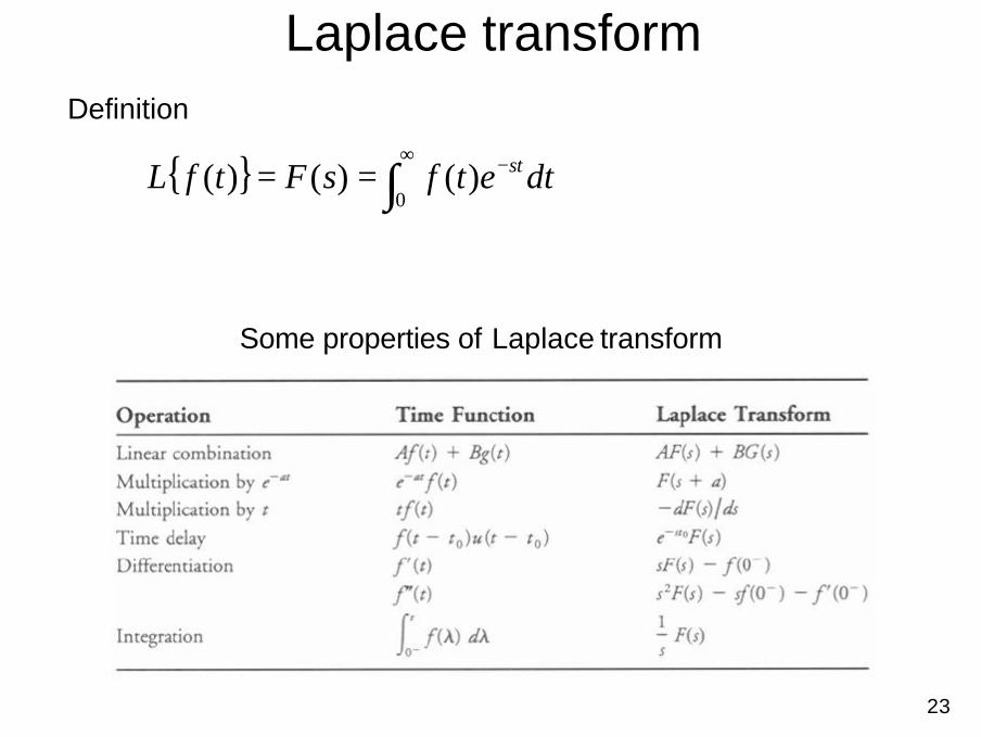
Laplace transform
∫∞ −==0
)()()( dtetfsFtfL st
Definition
Some properties of Laplace transform
24
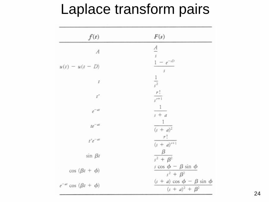
Laplace transform pairs
25
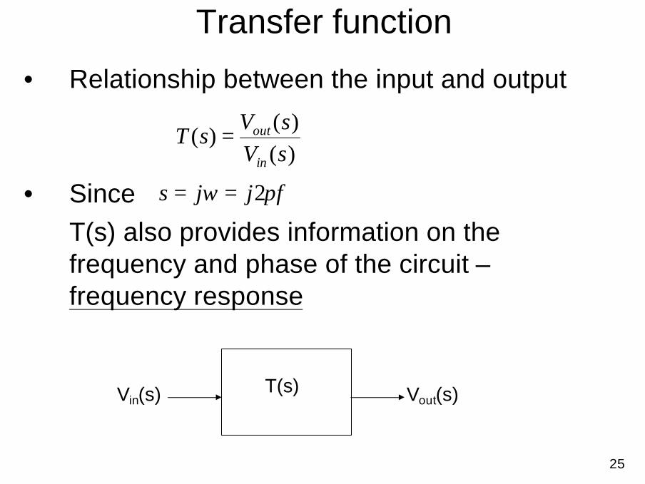
Transfer function
• Relationship between the input and output
• Since T(s) also provides information on the frequency and phase of the circuit –frequency response
)()(
)(sVsV
sTin
out=
fjjs πω 2==
T(s)Vin(s) Vout(s)
26
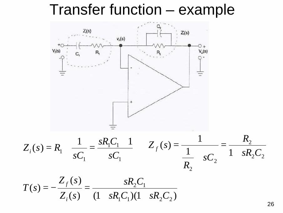
Transfer function – example
1
11
11
11)(
sCCsR
sCRsZ i
+=+=
)1)(1()(
)()(
2211
12
CsRCsRCsR
sZ
sZsT
i
f
++=−=
22
2
22
111
)(CsR
R
sCR
sZ f +=
+=
27
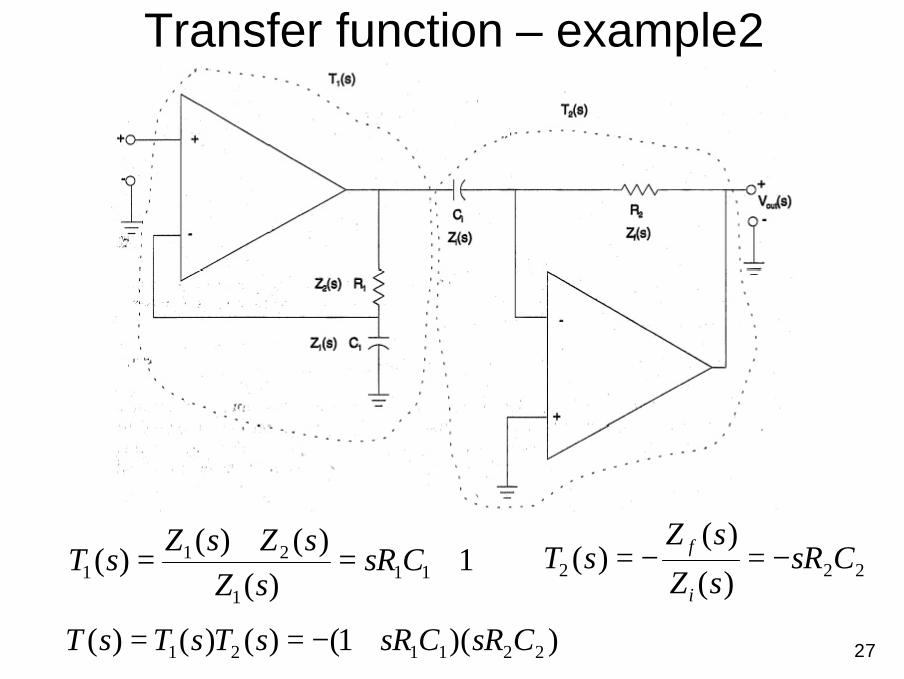
Transfer function – example2
1)(
)()()( 11
1
211 +=
+= CsR
sZsZsZ
sT
))(1()()()( 221121 CsRCsRsTsTsT +−==
222 )(
)()( CsR
sZ
sZsT
i
f −=−=
28
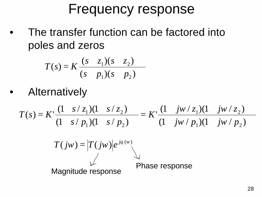
Frequency response
• The transfer function can be factored into poles and zeros
• Alternatively
⋅⋅⋅++⋅⋅⋅++
=))(())((
)(21
21
pspszszs
KsT
⋅⋅⋅++⋅⋅⋅++
=⋅⋅⋅++⋅⋅⋅++
=)/1)(/1()/1)(/1(
')/1)(/1()/1)(/1(
')(21
21
21
21
pjpjzjzj
Kpspszszs
KsTωωωω
)()()( ωθωω jejTjT =
Phase responseMagnitude response
29
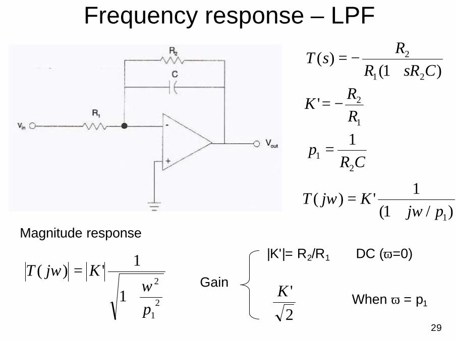
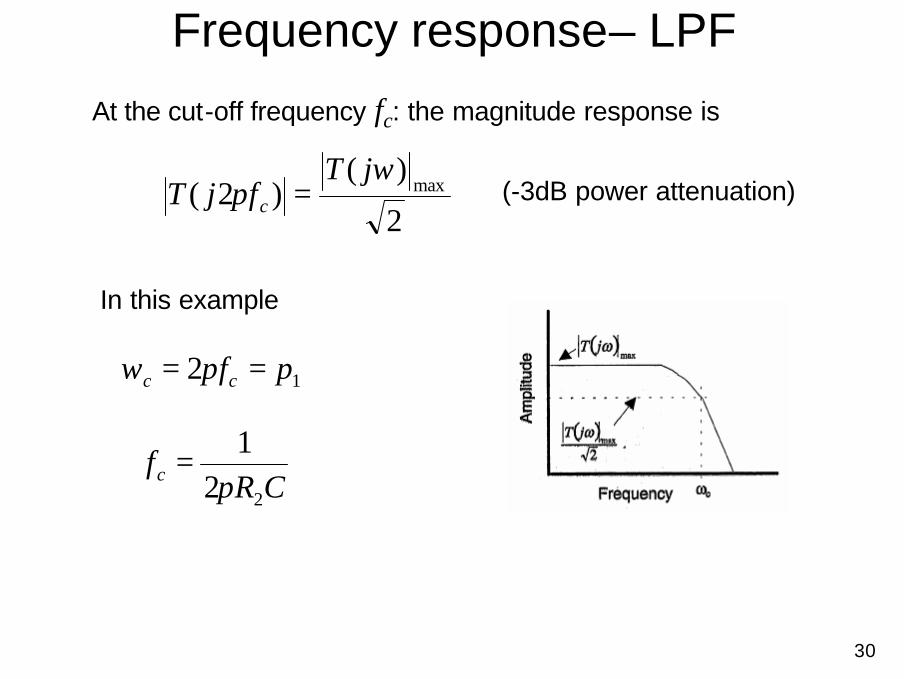
Frequency response – LPF
)1()(
21
2
CsRRR
sT+
−=
1
2'RR
K −=
CRp
21
1=
)/1(1
')(1pj
KjTω
ω+
=
21
2
1
1')(
p
KjTω
ω
+
=
Magnitude response
|K'|= R2/R1 DC (ω=0)
Gain
2'K When ω = p1
30
Frequency response– LPF
CRfc
221
π=∴
2
)()2( max
ωπ
jTfjT c =
At the cut-off frequency fc: the magnitude response is
In this example
12 pfcc == πω
(-3dB power attenuation)
31
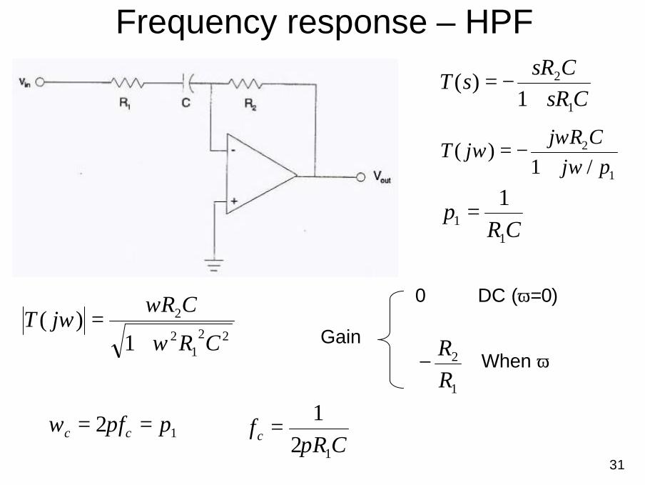
Frequency response – HPF
CsRCsR
sT1
2
1)(
+−=
1
2
/1)(
pjCRj
jTω
ωω
+−=
CRp
11
1=
221
2
2
1)(
CR
CRjT
ω
ωω
+=
0 DC (ω=0)
Gain
1
2
RR
− When ω→∞
CRfc
121
π=∴12 pfcc == πω
32
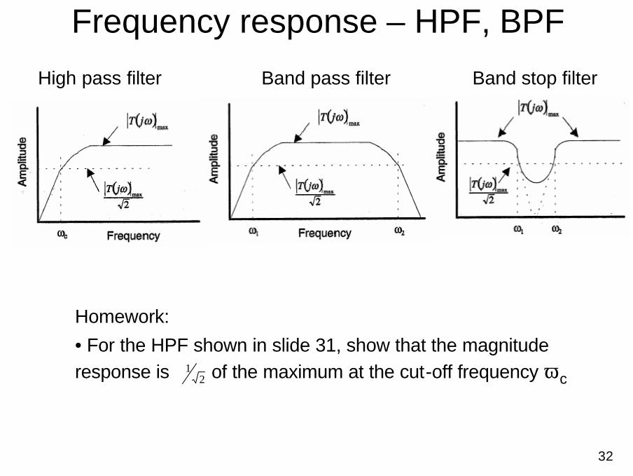
Frequency response – HPF, BPF
Homework:
•For the HPF shown in slide 31, show that the magnitude response is of the maximum at the cut-off frequency ωc
High pass filter Band pass filter Band stop filter
21
33
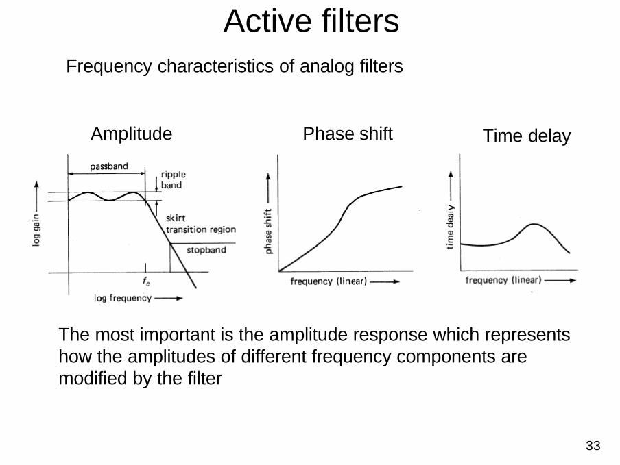
Active filtersFrequency characteristics of analog filters
Amplitude Phase shift Time delay
The most important is the amplitude response which represents how the amplitudes of different frequency components are modified by the filter
34
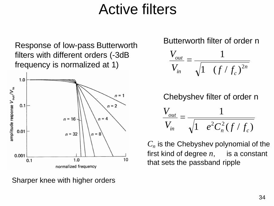
Active filters
)/(1
122
cnin
out
ffCeVV
+=
ncin
out
ffVV
2)/(1
1
+=
Response of low-pass Butterworth filters with different orders (-3dB frequency is normalized at 1)
Butterworth filter of order n
Chebyshev filter of order n
Cn is the Chebyshev polynomial of the first kind of degree n, ε is a constant that sets the passband ripple
Sharper knee with higher orders
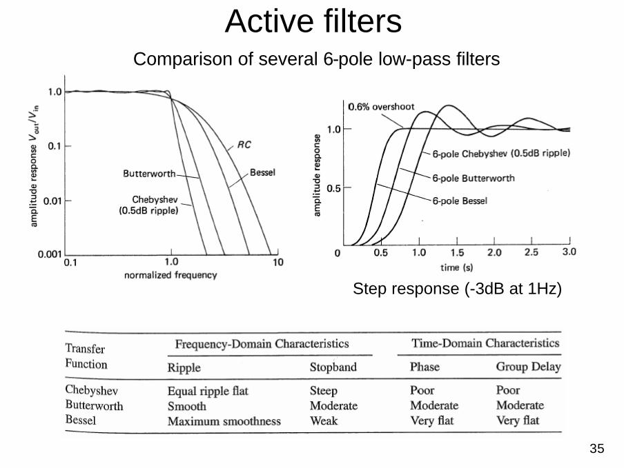
35
Active filtersComparison of several 6-pole low-pass filters
Step response (-3dB at 1Hz)
36
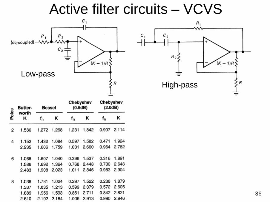
Active filter circuits – VCVS
Low-passHigh-pass
37
VCVS filter design
cfRC
π21
=
cn ffRC
π21
=
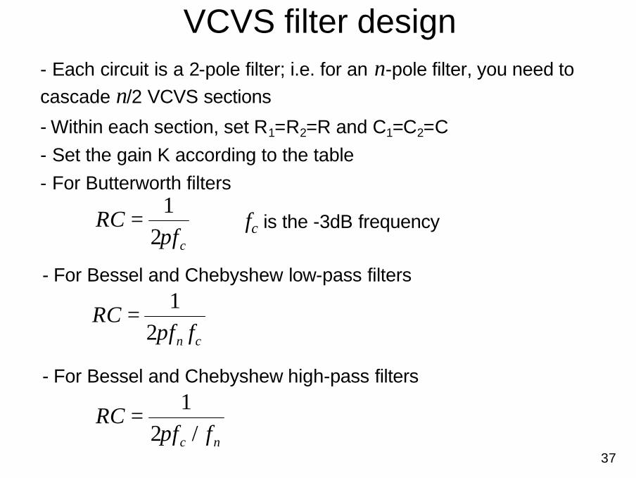
- Each circuit is a 2-pole filter; i.e. for an n-pole filter, you need to cascade n/2 VCVS sections
- Within each section, set R1=R2=R and C1=C2=C- Set the gain K according to the table- For Butterworth filters
nc ffRC
/21
π=
fc is the -3dB frequency
- For Bessel and Chebyshew low-pass filters
- For Bessel and Chebyshew high-pass filters
38
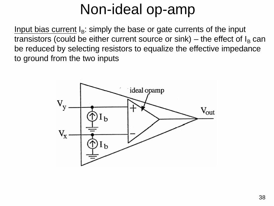
Non-ideal op-ampInput bias current IB: simply the base or gate currents of the input transistors (could be either current source or sink) – the effect of IB can be reduced by selecting resistors to equalize the effective impedance to ground from the two inputs
39
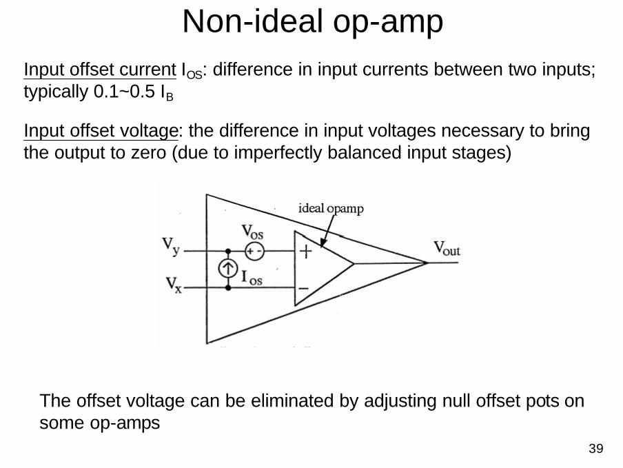
Non-ideal op-ampInput offset current IOS: difference in input currents between two inputs; typically 0.1~0.5 IB
Input offset voltage: the difference in input voltages necessary to bring the output to zero (due to imperfectly balanced input stages)
The offset voltage can be eliminated by adjusting null offset pots on some op-amps
40
Non-ideal op-amp
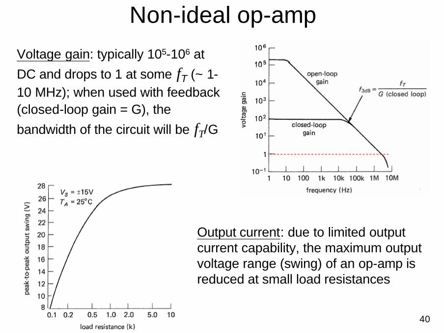
Voltage gain: typically 105-106 at
DC and drops to 1 at some fT (~ 1-10 MHz); when used with feedback (closed-loop gain = G), the
bandwidth of the circuit will be fT/G
Output current: due to limited output current capability, the maximum output voltage range (swing) of an op-amp is reduced at small load resistances
41
Practical considerations
• Negative feedback (resistor between the output and the inverted input terminal) provides a linear input/output response and in general stability of the circuit
• Choose resistor values 1kΩ-1MΩ (best 10kΩ–100kΩ)
• Match input impedances of the two inputs to improve CMRR
• Equalize the effective resistance to ground at the two input terminals to minimize the effects of IB
42
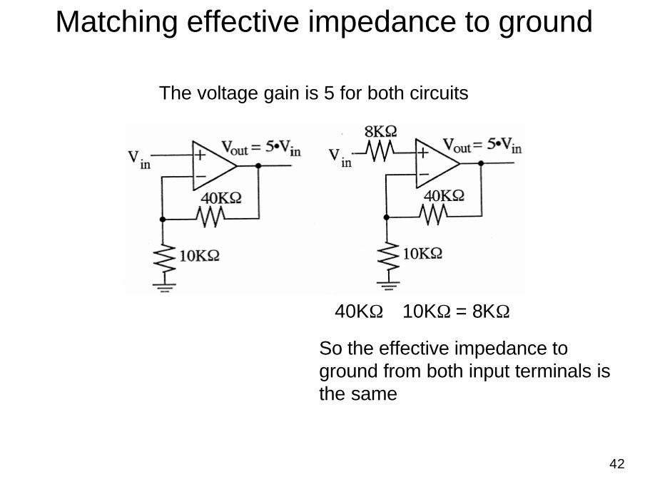
Matching effective impedance to ground
The voltage gain is 5 for both circuits
40KΩ∥10KΩ = 8KΩ
So the effective impedance to ground from both input terminals is the same
43
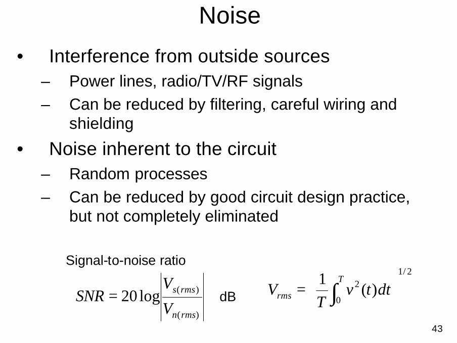
Noise
• Interference from outside sources– Power lines, radio/TV/RF signals– Can be reduced by filtering, careful wiring and
shielding
• Noise inherent to the circuit– Random processes– Can be reduced by good circuit design practice,
but not completely eliminated
)(
)(log20rmsn
rmss
V
VSNR =
Signal-to-noise ratio2/1
0
2 )(1
= ∫
T
rms dttvT
VdB
44
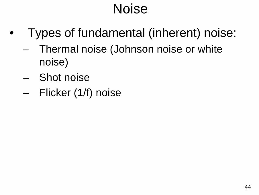
Noise
• Types of fundamental (inherent) noise:– Thermal noise (Johnson noise or white
noise)– Shot noise– Flicker (1/f) noise
45
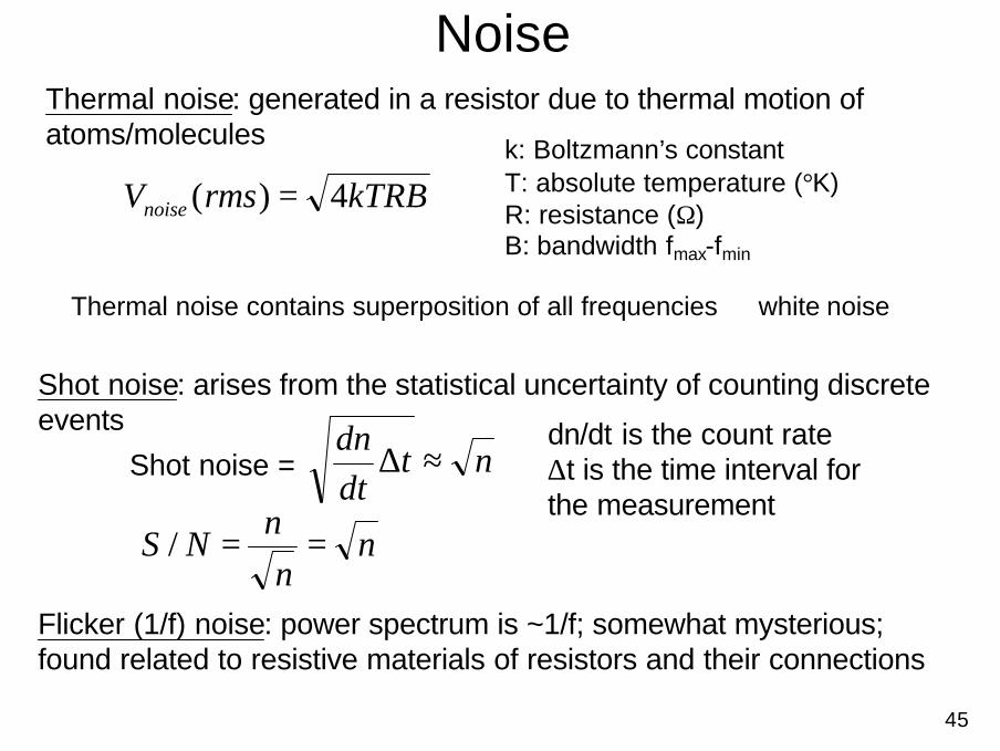
Noise
kTRBrmsVnoise 4)( =k: Boltzmann’s constantT: absolute temperature (°K)R: resistance (Ω)B: bandwidth fmax-fmin
Thermal noise: generated in a resistor due to thermal motion of atoms/molecules
Thermal noise contains superposition of all frequencies ⇒ white noise
nn
nNS ==/
Shot noise: arises from the statistical uncertainty of counting discrete events
Flicker (1/f) noise: power spectrum is ~1/f; somewhat mysterious; found related to resistive materials of resistors and their connections
Shot noise =dn/dt is the count rate∆t is the time interval for the measurement
ntdtdn
≈∆
46
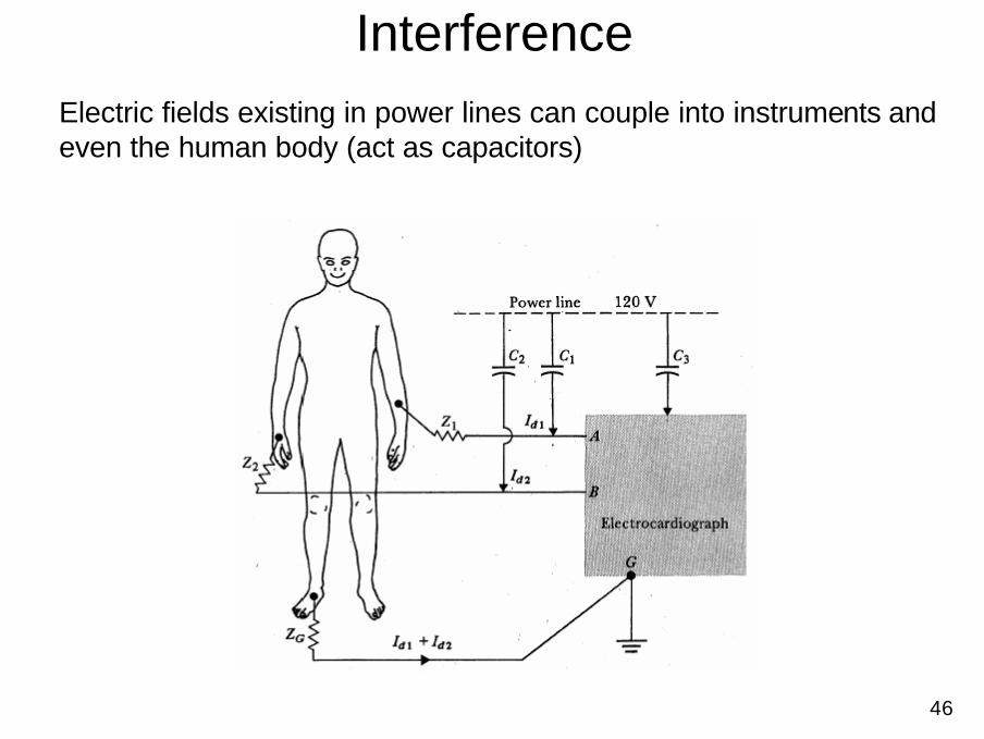
InterferenceElectric fields existing in power lines can couple into instruments and even the human body (act as capacitors)
47
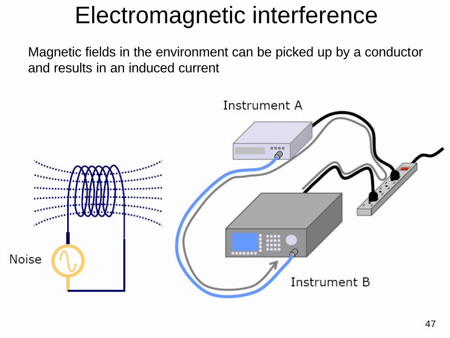
Electromagnetic interferenceMagnetic fields in the environment can be picked up by a conductor and results in an induced current
48
Electromagnetic interference
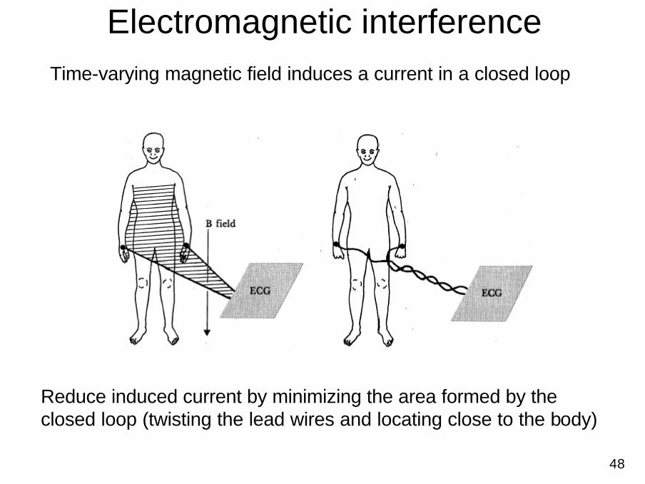
Reduce induced current by minimizing the area formed by the closed loop (twisting the lead wires and locating close to the body)
Time-varying magnetic field induces a current in a closed loop
49
Electrical safety
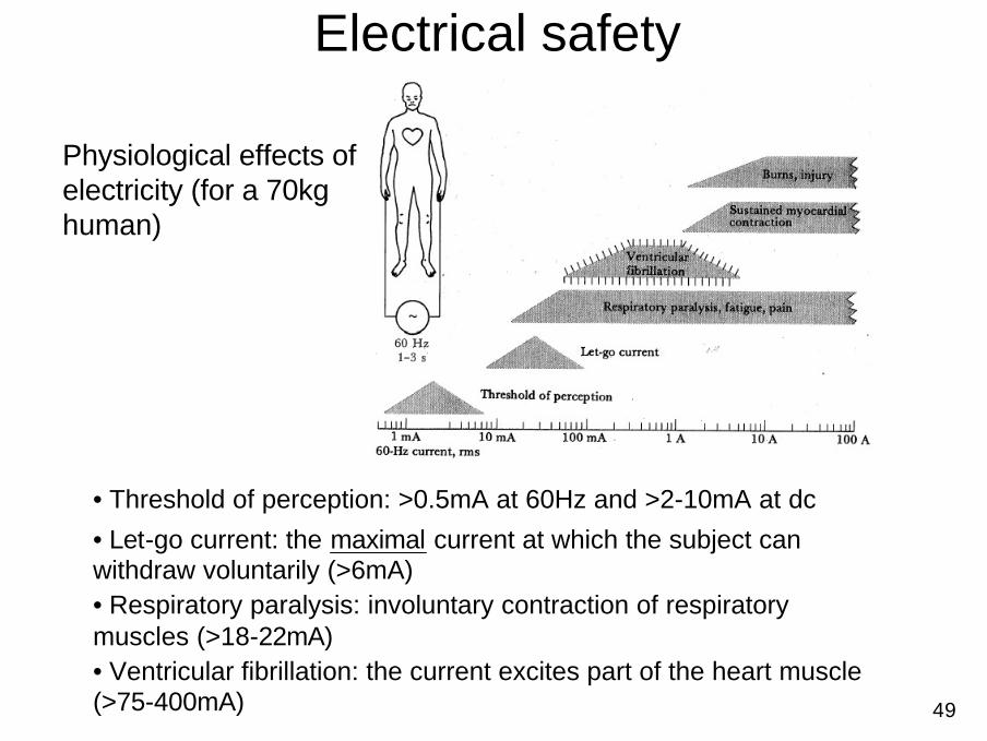
Physiological effects of electricity (for a 70kg human)
•Threshold of perception: >0.5mA at 60Hz and >2-10mA at dc
•Let-go current: the maximal current at which the subject can withdraw voluntarily (>6mA)•Respiratory paralysis: involuntary contraction of respiratory muscles (>18-22mA)•Ventricular fibrillation: the current excites part of the heart muscle (>75-400mA)
50
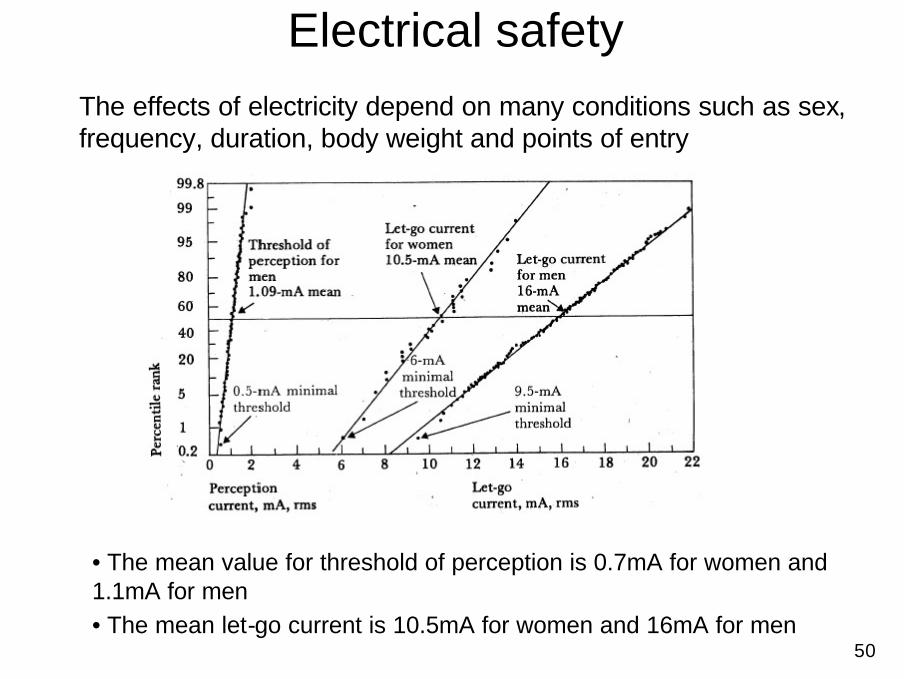
Electrical safetyThe effects of electricity depend on many conditions such as sex, frequency, duration, body weight and points of entry
•The mean value for threshold of perception is 0.7mA for women and 1.1mA for men•The mean let-go current is 10.5mA for women and 16mA for men
51
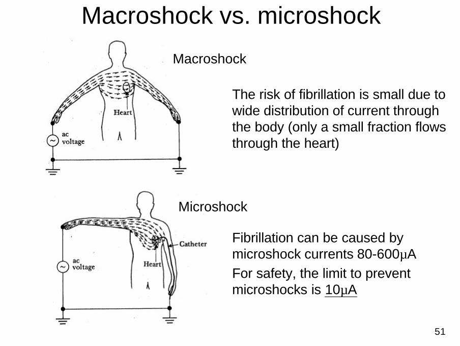
Macroshock vs. microshock
Microshock
The risk of fibrillation is small due to wide distribution of current through the body (only a small fraction flows through the heart)
Fibrillation can be caused by microshock currents 80-600µAFor safety, the limit to prevent microshocks is 10µA
Macroshock
52
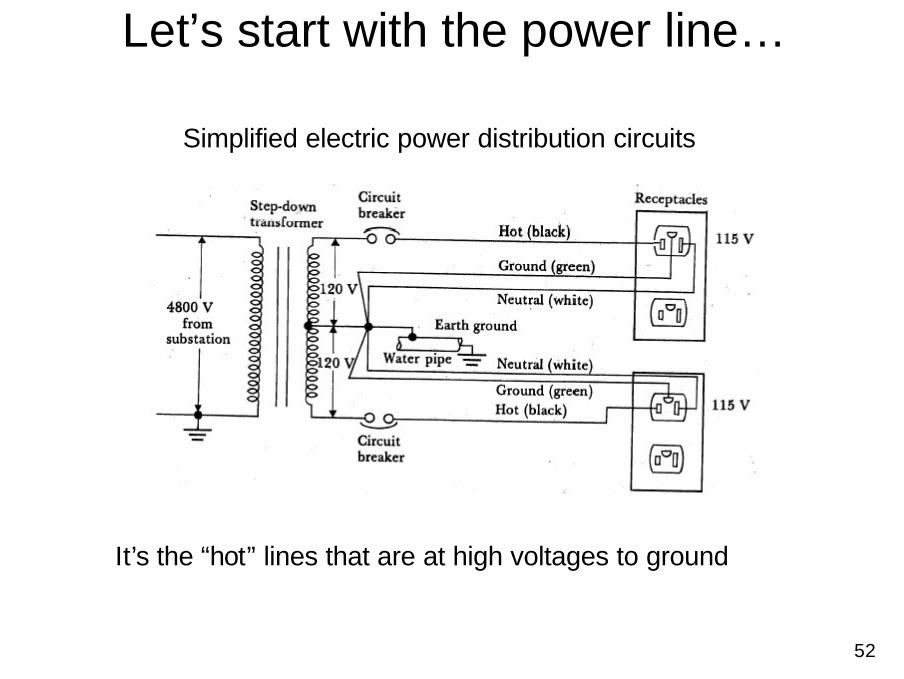
Let’s start with the power line…
Simplified electric power distribution circuits
It’s the “hot” lines that are at high voltages to ground
53
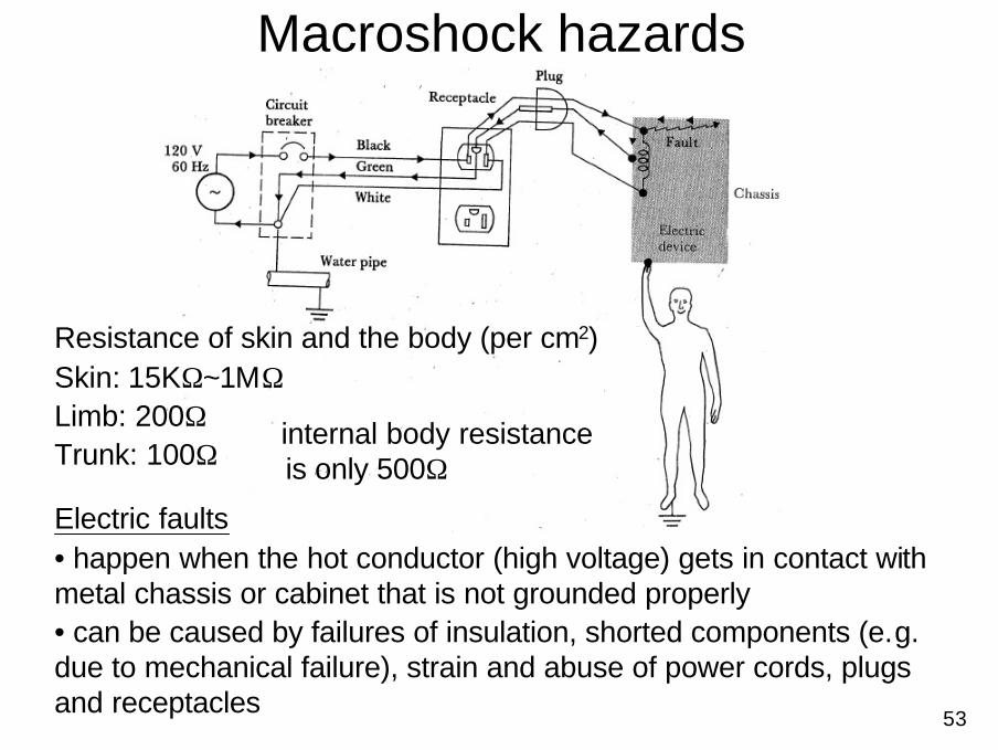
Macroshock hazards
Resistance of skin and the body (per cm2)Skin: 15KΩ~1MΩLimb: 200ΩTrunk: 100Ω
Electric faults•happen when the hot conductor (high voltage) gets in contact with metal chassis or cabinet that is not grounded properly•can be caused by failures of insulation, shorted components (e.g. due to mechanical failure), strain and abuse of power cords, plugs and receptacles
⇒ internal body resistanceis only 500Ω
54
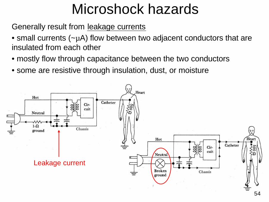
Microshock hazardsGenerally result from leakage currents•small currents (~µA) flow between two adjacent conductors that are insulated from each other•mostly flow through capacitance between the two conductors•some are resistive through insulation, dust, or moisture
Leakage current
55
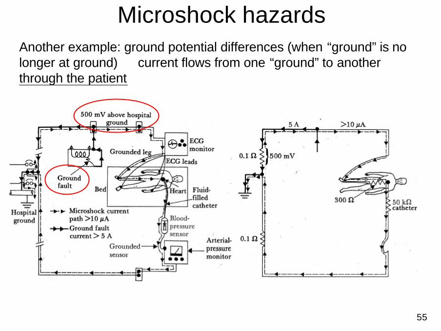
Microshock hazardsAnother example: ground potential differences (when “ground”is no longer at ground) ⇒ current flows from one “ground”to another through the patient
56
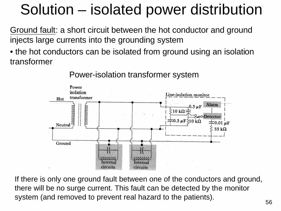
Solution – isolated power distributionGround fault: a short circuit between the hot conductor and ground injects large currents into the grounding system• the hot conductors can be isolated from ground using an isolation transformer
Power-isolation transformer system
If there is only one ground fault between one of the conductors and ground, there will be no surge current. This fault can be detected by the monitor system (and removed to prevent real hazard to the patients).

57
Solution – grounding system
•All the receptacle grounds and conductive surfaces in the vicinity of the patient are connected to the patient-equipment grounding point (with resistance = 0.15Ω)•The difference in potential between the conductive surfaces must be = 40mV•Each patient-equipment grounding point is connected individually to a reference grounding point that is in turn connected to the building ground
58
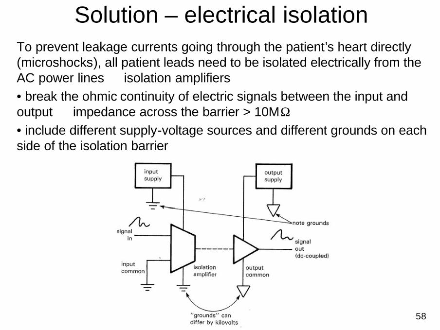
Solution – electrical isolationTo prevent leakage currents going through the patient’s heart directly (microshocks), all patient leads need to be isolated electrically from the AC power lines ⇒ isolation amplifiers•break the ohmic continuity of electric signals between the input and output ⇒ impedance across the barrier > 10MΩ• include different supply-voltage sources and different grounds on each side of the isolation barrier
59
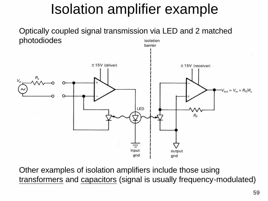
Isolation amplifier exampleOptically coupled signal transmission via LED and 2 matched photodiodes
Other examples of isolation amplifiers include those using transformers and capacitors (signal is usually frequency-modulated)
60
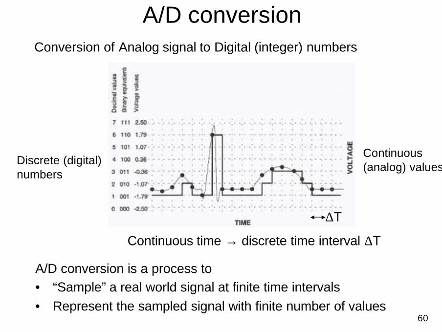
A/D conversionConversion of Analog signal to Digital (integer) numbers
Continuous (analog) valuesDiscrete (digital)
numbers
Continuous time → discrete time interval ∆T
A/D conversion is a process to• “Sample”a real world signal at finite time intervals• Represent the sampled signal with finite number of values
∆T
61
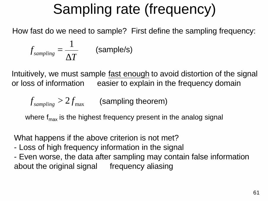
Sampling rate (frequency)How fast do we need to sample? First define the sampling frequency:
Tfsampling ∆
=1
max2 ffsampling >
(sample/s)
Intuitively, we must sample fast enough to avoid distortion of the signal or loss of information ⇒ easier to explain in the frequency domain
where fmax is the highest frequency present in the analog signal
(sampling theorem)
What happens if the above criterion is not met?- Loss of high frequency information in the signal- Even worse, the data after sampling may contain false information about the original signal ⇒ frequency aliasing
62
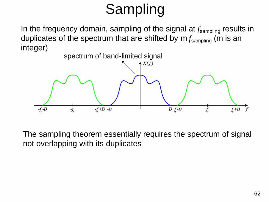
SamplingIn the frequency domain, sampling of the signal at fsampling results in duplicates of the spectrum that are shifted by m⋅fsampling (m is an integer)
spectrum of band-limited signal
The sampling theorem essentially requires the spectrum of signalnot overlapping with its duplicates
63
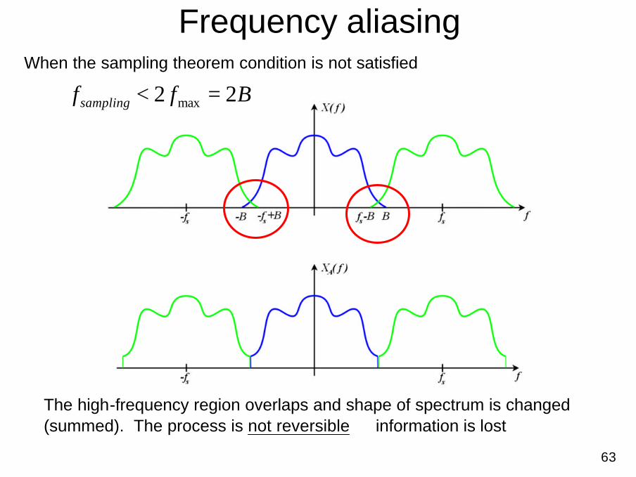
Frequency aliasingWhen the sampling theorem condition is not satisfied
Bffsampling 22 max =<
The high-frequency region overlaps and shape of spectrum is changed (summed). The process is not reversible ⇒ information is lost
64
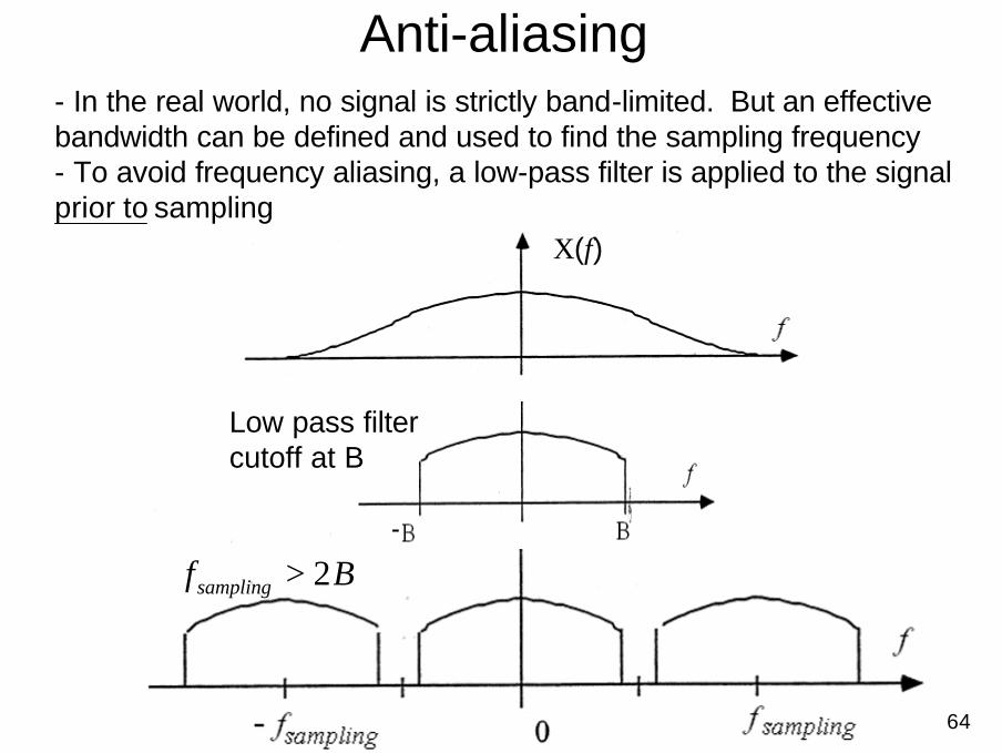
Anti-aliasing- In the real world, no signal is strictly band-limited. But an effective bandwidth can be defined and used to find the sampling frequency- To avoid frequency aliasing, a low-pass filter is applied to the signal prior to sampling
X(f)
Low pass filter cutoff at B
Bf sampling 2>
65
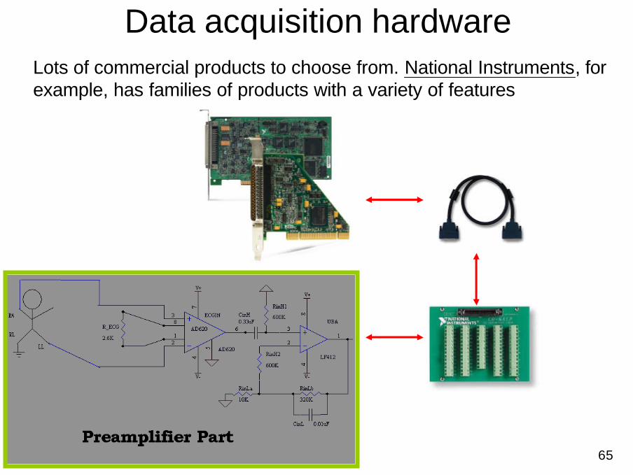
Data acquisition hardwareLots of commercial products to choose from. National Instruments, for example, has families of products with a variety of features
66
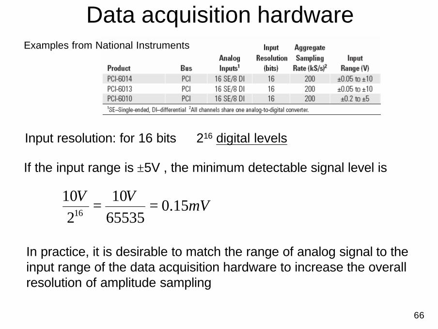
Data acquisition hardware
Input resolution: for 16 bits ⇒ 216 digital levels
If the input range is ±5V , the minimum detectable signal level is
mVVV
15.06553510
210
16 ==
In practice, it is desirable to match the range of analog signal to the input range of the data acquisition hardware to increase the overall resolution of amplitude sampling
Examples from National Instruments
67
References
• The Art of Electronics (2nd ed.), by Paul Horowitz and Winfield Hill
– Ch5: Active filters– Ch7: Precision circuits and low-noise
techniques
• Medical Instrumentation: application and design, 3rd ed., edited by John G. Webster
– Ch3: Amplifiers and Signal Processing– Ch14: Physiological effects of electricity