Embed Size (px)
Citation preview

-otl
aA
DD
76
1/
02
02
+fejaa
e*GMFTSH
9
NBSI 5-4900-46-259-879 )detnirp(
NBSI 2-5900-46-259-879 )fdp(
NSSI 4394-9971 )detnirp(
NSSI 2494-9971 )fdp(
ytisrevinU otlaA
gnireenignE lacirtcelE fo loohcS
gnireenigneonaN dna scinortcelE fo tnemtrapeD
fi.otlaa.www
+ SSENISUB YMONOCE
+ TRA
+ NGISED ERUTCETIHCRA
+ ECNEICS
YGOLONHCET
REVOSSORC
LAROTCOD SNOITATRESSID
ne
nitt
em
eL
iroJ
yg
olo
nhc
et r
otsi
sna
rt t
cef
fe-
dle
fi N-
III
laix
ati
pe
ot s
tn
em
evor
pmI
yti
srev
in
U otl
aA
0202
gnireenigneonaN dna scinortcelE fo tnemtrapeD
laixatipe ot stnemevorpmI rotsisnart tceffe-dlefi N-III
ygolonhcet
nenittemeL iroJ
LAROTCOD SNOITATRESSID

Printed matter4041-0619
NO
RDIC
SWAN ECOLABE
L


Preface
The research presented in this thesis was carried out at the Department ofElectronics and Nanoengineering, Micronova, at Aalto University School ofElectrical Engineering in addition to the Microsystems Technology Laboratoriesat the Massachusetts Institute of Technology.
I want to express my gratitude to Professor Markku Sopanen, the supervisorof this thesis for this great opportunity, Professor Tomás Palacios, supervisorof my work at MIT, and Professor Hironori Okumura (University of Tsukuba)for the N-polar AlN project. I am very grateful to Dr. Sami Suihkonen, thethesis advisor, for his guidance, help and expertise during this work, and theinteresting discussions on all things scientific and general.
I would like to thank Prof. Turkka Tuomi for organizing the SR-XRT mea-surement visits. Dr. Atte Haapalinna must also be thanked and Okmetic Oyjfor providing the Si and SOI substrates. Thank you, co-authors, co-workersand friends Mr. Iurii Kim, Dr. Christoffer Kauppinen, Dr. Mariusz Rudzínski,Dr. Justyna Grzonka, Dr. Alexander Pyymäki-Perros, Dr. Perttu Sippola, Dr.Henri Jussila, Dr. Lauri Riuttanen, Dr. Mikael Broas, Dr. John Rönn, Mr. KirillIsakov, Mr. Vladislav Khayrudinov, Dr. Taneli Juntunen, Dr. Tuomas Haggren,Dr. Jani Oksanen, Dr. Toufik Sadi, Dr. Ivan Radevici, Ms. Heli Seppänen, Ms.Camilla Tossi, Prof. Harri Lipsanen and Prof. Ilkka Tittonen. I wish to thankthe inhabitants of our corner office — The LED cave — although a change in thename is now in order, we truly had something special during these years insideand outside of work. Thanks to all the people of Micronova for the friendly anda pleasant working environment. I thank the Aalto Nanofab and VTT for thenanofabrication facilities and invaluable process support.
I would like to especially thank Mr. Nadim Chowdhury, officemate and friendat MIT, for his help with the transistor fabrication and lively discussions. Thanksto all Palacios group members for the pleasant working environment and makingme feel at home at MIT. I would also like to thank Dr. Ahmad Zubair, Mr. JoshuaPerozek, Mr. Marek Hempel, Ms. Elaine Mcvay and Mr. Mengyang Yuanfor help with the processing and characterization, in addition to Mr. JosephBaylon for helping with practical matters. I want to thank the staff of theMicrosystems Technology Laboratories for the nanofabrication facilities and
vii

Preface
process support. I thank all the people who made my visit possible and enjoyable,Fulbright Finland, people on Clinton Street and especially our group of Finns inCambridge, unapologetically known as The Finnish Mafia.
Finally, my warmest thanks to my family and friends for all the support duringmy life and studies, and to Mima.
This work has been partly funded by the Aalto ELEC Doctoral School of AaltoUniversity, Aalto University Foundation for Science and Technology, FulbrightFinland Foundation, and the Walter Alström Foundation. I am grateful for theirgenerosity.
September 1, 2019,
Jori Lemettinen
viii

Contents
Preface vii
Contents ix
List of Publications xi
Author’s Contribution xiii
Abbreviations xv
Symbols xix
1. Introduction 1
2. III-N semiconductors 52.1 Crystal structure . . . . . . . . . . . . . . . . . . . . . . . . . . . . 92.2 Crystallographic defects . . . . . . . . . . . . . . . . . . . . . . . 12
3. III-N growth 153.1 Substrates for III-N epitaxy . . . . . . . . . . . . . . . . . . . . . 173.2 Metal-organic vapor phase epitaxy . . . . . . . . . . . . . . . . . 213.3 Thermodynamics of crystal growth . . . . . . . . . . . . . . . . . 243.4 Surface kinetics of crystal growth . . . . . . . . . . . . . . . . . . 253.5 N-polar III-N epitaxy . . . . . . . . . . . . . . . . . . . . . . . . . 27
4. Characterization methods 314.1 In-situ monitoring . . . . . . . . . . . . . . . . . . . . . . . . . . . 314.2 Atomic force microscope . . . . . . . . . . . . . . . . . . . . . . . . 344.3 Scanning electron microscope . . . . . . . . . . . . . . . . . . . . 354.4 Selective etching . . . . . . . . . . . . . . . . . . . . . . . . . . . . 364.5 X-ray diffraction . . . . . . . . . . . . . . . . . . . . . . . . . . . . 37
4.5.1 High-resolution X-ray diffraction setup . . . . . . . . 384.5.2 Reciprocal space . . . . . . . . . . . . . . . . . . . . . . 404.5.3 Measurement types and geometries . . . . . . . . . . 41
ix

Contents
4.5.4 Threading dislocation density . . . . . . . . . . . . . . 434.6 Synchrotron X-ray topography . . . . . . . . . . . . . . . . . . . . 44
5. III-N field effect transistors 475.1 Metal-semiconductor field effect transistor . . . . . . . . . . . . 495.2 Formation of two-dimensional electron gas in HEMTs . . . . . 505.3 Spatial distribution of two-dimensional electron gas in HEMTs 535.4 Nitrogen-polar HEMT . . . . . . . . . . . . . . . . . . . . . . . . . 545.5 Operation of a III-N HEMT . . . . . . . . . . . . . . . . . . . . . 565.6 Normally-off/enhancement-mode HEMT . . . . . . . . . . . . . . 58
6. Nitrogen-polar AlGaN/AlN PolFET 636.1 N-polar unintentionally doped AlN MOVPE growth . . . . . . . 666.2 N-polar resistive AlN MOVPE growth . . . . . . . . . . . . . . . 686.3 N-polar PolFET fabrication and electrical characteristics . . . . 71
7. Improvements to metal-polar III-N FETs 757.1 MOVPE growth of GaN on 6-inch SOI-substrates . . . . . . . . 757.2 P-channel AlGaN/GaN HEMT on Si . . . . . . . . . . . . . . . . 767.3 Si-ion implanted AlN MESFET . . . . . . . . . . . . . . . . . . . 78
8. Prospects of III-N electronics markets 818.1 Power electronics . . . . . . . . . . . . . . . . . . . . . . . . . . . . 828.2 RF electronics . . . . . . . . . . . . . . . . . . . . . . . . . . . . . . 83
9. Summary 87
References 89
Publications 101
x

List of Publications
This thesis consists of an overview and of the following publications which arereferred to in the text by their Roman numerals.
I Jori Lemettinen, Christoffer Kauppinen, Marius Rudzinski, Atte Haapalinna,Turkka O. Tuomi, and Sami Suihkonen. MOVPE growth of GaN on 6-inch SOI-substrates: effect of substrate parameters on layer quality and strain. Semi-conductor Science and Technology, 32, 4, 045003, https://doi.org/10.1088/1361-6641/aa5942, March 2017.
II Nadim Chowdhury, Jori Lemettinen, Qingyun Xie, Yuhao Zhang, Nitul S.Rajput, Peng Xiang, Kai Cheng, Sami Suihkonen, Han Wui Then and TomásPalacios. p-Channel GaN Transistor based on p-GaN/AlGaN/GaN on Si. IEEEElectron Device Letters, https://doi.org/10.1109/LED.2019.2916253, May 2019.
III Jori Lemettinen, Hironori Okumura, Iurii Kim, Marius Rudzinski, JustynaGrzonka, Tomàs Palacios, and Sami Suihkonen. MOVPE growth of nitrogen-and aluminum-polar AlN on 4H-SiC. Journal of Crystal Growth, 487, 50-56,https://doi.org/10.1016/j.jcrysgro.2018.02.020, February 2018.
IV Jori Lemettinen, Hironori Okumura, Iurii Kim, Christoffer Kauppinen,Tomàs Palacios, and Sami Suihkonen. MOVPE growth of N-polar AlN on4H-SiC: Effect of substrate miscut on layer quality. Journal of Crystal Growth,487, 12-16, https://doi.org/10.1016/j.jcrysgro.2018.02.0132, February 2018.
V Jori Lemettinen, Hironori Okumura, Tomás Palacios and Sami Suihkonen. N-polar AlN buffer growth by MOVPE for transistor applications. Applied PhysicsExpress, 11, 10, 101002, https://doi.org/10.7567/APEX.11.101002, September2018.
VI Jori Lemettinen, Nadim Chowdhury, Hironori Okumura, Iurii Kim, Sami
xi

List of Publications
Suihkonen and Tomás Palacios. Nitrogen-Polar Polarization-Doped Field-Effect Transistor based on Al0.8Ga0.2N/AlN on SiC with drain current over 100mA/mm. IEEE Electron Device Letters, https://doi.org/10.1109/LED.2019.2923902,June 2019.
VII Hironori Okumura, Sami Suihkonen, Jori Lemettinen, Akira Uedono, YuhaoZhang, Daniel Piedra and Tomás Palacios. AlN metal-semiconductor field-effect transistors using Si-ion implantation. Japanese Journal of AppliedPhysics, 57, 4S, 04FR11, https://doi.org/10.7567/JJAP.57.04FR11, March 2018.
xii

Author’s Contribution
Publication I: “MOVPE growth of GaN on 6-inch SOI-substrates:effect of substrate parameters on layer quality and strain”
The author wrote the manuscript, designed and performed the epitaxy, per-formed the cross-sectional SEM, XRD, SR-XRT, reflectance and vertical break-down measurements. Co-authors performed the selective etching measurementand participated in vertical breakdown, reflectance, SR-XRT measurements andin writing the manuscript
Publication II: “p-Channel GaN Transistor based onp-GaN/AlGaN/GaN on Si”
The author participated in the gate recess etching, performed the AFM charac-terization and participated in writing the manuscript.
Publication III: “MOVPE growth of nitrogen- and aluminum-polar AlNon 4H-SiC”
The author wrote the manuscript, designed and performed the epitaxy andperformed XRD, SEM and AFM measurements. Co-authors performed theselective etching measurement and participated in epitaxy in addition to SEMmeasurements and in writing the manuscript.
xiii

Author’s Contribution
Publication IV: “MOVPE growth of N-polar AlN on 4H-SiC: Effect ofsubstrate miscut on layer quality”
The author wrote the manuscript, designed and performed the epitaxy and per-formed XRD, SEM and AFM measurements. Co-authors participated in epitaxyin addition to AFM and SEM measurements and in writing the manuscript.
Publication V: “N-polar AlN buffer growth by MOVPE for transistorapplications”
The author wrote the manuscript, designed and performed the epitaxy andperformed XRD measurements. Co-authors performed the transistor fabrication,electrical characterization and participated in writing the manuscript. TheSIMS measurements were outsourced to EAG laboratories.
Publication VI: “Nitrogen-Polar Polarization-Doped Field-EffectTransistor based on Al0.8Ga0.2N/AlN on SiC with drain current over100 mA/mm”
The author wrote the manuscript, designed and performed the epitaxy, transis-tor fabrication and electrical characterization. Co-authors participated in thetransistor fabrication, electrical characterization and in writing the manuscript.
Publication VII: “AlN metal-semiconductor field-effect transistorsusing Si-ion implantation”
The author performed the post-implantation annealing and participated inwriting the manuscript.
xiv

Abbreviations
2D two-dimensional
2DEG two-dimensional electron gas
2DHG two-dimensional hole gas
3D three-dimensional
3DEG three-dimensional electron gas
5G fifth generation
AC alternating current
AFM atomic force microscope
Al aluminum
AlGaAs aluminum gallium arsenide
AlGaN aluminum gallium nitride
AlN aluminum nitride
atm atmosphere
Au gold
B boron
BFOM Baliga’s figure of merit
BiCMOS bipolar and CMOS
BOX buried oxide
CCD charge-coupled device
CMOS complementary metal–oxide–semiconductor
xv

Abbreviations
Cp2Mg bis-cyclopentadienyl magnesium
Cu copper
D-mode depletion-mode
DC direct current
DSE defect selective etching
E-mode enhancement-mode
FET field-effect transistor
FM Frank-van Der Merwe
FOM figure of merit
Ga gallium
Ga2O3 gallium oxide
GaAs gallium arsenide
GaN gallium nitride
H hydrogen
H3PO4 phosphoric acid
HBT heterojunction bipolar transistor
HEMT high electron mobility transistor
HRXRD high resolution X-ray diffraction
HVPE hydride vapor phase epitaxy
IGBT insulated-gate bipolar transistor
II-IV two-four
III-N three-nitride
III-V three-five
In indium
InGaAs indium gallium arsenide
InGaN indium gallium nitride
InN indium nitride
InP indium phosphide
xvi

Abbreviations
KOH potassium hydroxide
LDMOS laterally diffused MOSFET
LED light emitting diode
LT low temperature
MBE molecular beam epitaxy
MESFET metal-semiconductor field-effect transistor
Mg magnesium
ML monolayer
MMIC monolithic microwave integrated circuit
MOSFET metal-oxide field-effect transistor
MOVPE metalorganic vapor-phase epitaxy
N nitrogen
N2H4 hydrazine
NaOH potassium hydroxide
NH3 ammonia
Ni nickel
PolFET polarization-doped field-effect transistor
QCSE quantum-confined Stark effect
RC resistive-capacitive
RF radio-frequency
RSM reciprocal space map
SEM scanning electron microscope
Si silicon
Si2H6 disilane
SiC silicon carbide
SiH4 silane
SiO2 silicon dioxide
SK Stranski-Krastanov
xvii

Abbreviations
SOI silicon-on-insulator
SR-XRT synchrotron-radiation X-ray topography
SS subthreshold swing
SSL solid-state lighting
TaC tantalum carbide
TEGa triethylgallium
Ti titanium
TLK terrace-ledge-kink
TMAl trimethylaluminum
TMGa trimethylgallium
TMIn trimethylindium
TTD threading dislocation density
UID unintentionally doped
USD united states dollar
VW Volmer-Weber
XRD X-ray diffraction
xviii

Symbols
a In-plane lattice constant
c Out-of-plane lattice constant
b Burger’s vector
d thickness
EC conduction band
Ec critical electric field
E f Fermi level
Eg band-gap
ES surface donor states
EV valence band
g reflection miller indices or gas
gm transconductance
H diffraction vector
Id drain current
k0 incident beam wave vector
kb Boltzmann constant
ks diffracted beam wave vector
l liquid
Lg gate length
Lgd gate-to-drain distance
xix

Symbols
Lgs gate-to-source distance
me electron mass
n order of diffraction
n(z) electron concentration
Na(z) acceptor concentration
Nd(z) donor concentration
ns sheet electron density
p(z) hole concentration
Q reciprocal space coordinate
q elementary charge
Ron on-resistance
s solid
T temperature
u dislocation line direction
V voltage or potential
Vdd positive supply voltage
Vds drain to source voltage
Vgs gate to source voltage
vsat saturated electron velocity
Vt threshold voltage
� reduced Planck’s constant
β width of a diffraction peak
ε dielectric constant
Θ epitaxial layer thickness in monolayers
θ angle between incident and diffracted beam
θb surface barrier height
κ thermal conductivity
λ wavelength
xx

Symbols
μe electron mobility
σ charge
Ψ(z) wave function
ω angle between sample surface and diffracted beam
xxi


1. Introduction
The adoption of III-nitride (III-N) semiconductor (GaN, AlN, InN) based devicescan be seen as the latest stage in the quest for higher power density and effi-ciency. This spectacle has been ongoing since the dawn of civilization, althoughaccelerating significantly during and after the industrial revolution. Fromburning coal to steam engines, practical electricity usage started with the devel-opment of a generator demonstrated in 1871 [1]. From there, electromechanicalrelays were replaced by vacuum tubes, first demonstrated in 1904 [2]. However,a paradigm shift occurred when transistors and especially integrated circuitscame into use in 1947 and 1958, respectively [3,4]. Now the focus is no longeron creating large-sized objects, but rather on the possibility of small and wellintegrated components in a single apparatus as famously outlined in ’There’sPlenty of Room at the Bottom’ in 1959 [5]. These factors are not directly limitedby resources and manpower, but by the level of technology. After the advent ofsilicon (Si) complementary metal oxide semiconductor (CMOS) technology, thecomplexity of integrated circuits has doubled roughly every two years bringingunprecedented change and possibilities [6].
Interestingly, the current prominent compound semiconductor families, so-called traditional III-Vs (e.g., GaAs and InP) and III-Ns, both gained theirfoothold in the market of light-emitting applications [7,8]. This occurred becausesilicon could not be used as a light emitter due to an indirect band gap. Thebasic epitaxial and bulk crystal growth techniques for the III-Vs were discoveredand developed for the first infra-red and red light emitting diodes (LED) in1955 [9]. Furthermore, these techniques enabled the diode laser (1962), whichtogether with the optical fiber (1970s) forms the backbone of a data-drivensociety [10,11]. This shall be a lesson to future semiconductor materials to startfrom the simpler two-terminal devices, and especially light-emitting applications,which are powerful in capturing the imagination of young scientists.
Later, in 1970s it was discovered that GaAs field effect transistors (FETs) offera much higher operating frequency in comparison to that of silicon FETs [12,13].Even more remarkable cut-off frequencies were achieved with high electronmobility transistors (HEMTs) [13]. HEMT exploits clever band engineering by aheterostructure separating the dopants from the transistor channel. This allows
1

Introduction
the channel to retain the bulk charge carrier mobility regardless of the dopingdensity.
Similarly, both semiconductor families have their application in swords andploughshares [13,14]. Having demonstrated excellent mm-wave amplificationproperties in 1983, GaAs HEMTs were perfected in the 1990s for radio frequency(RF) applications through the further investment of defense funding [15–18].Some of the developed technologies were transferred to the mass market, andcurrently, GaAs RF power amplifiers are used in cell phone handsets and basestations [19].
GaN was proposed as the material for blue LEDs which cannot be realizedwith the traditional III-Vs [8]. Blue LEDs were long sought after to completethe visible spectrum with solid-state sources. However, no suitable materialcandidate existed as a wide and direct band gap is required. In the 1980s, bothGaN and II-IV semiconductors were considered [8]. While II-IVs were limitedby reliability, the momentum of GaN crystal growth studies were peteringout as single-crystalline material had not been demonstrated, despite yearsof research [8]. Eventually, device quality material was achieved (1988) in areactor type, metalorganic vapor-phase epitaxy (MOVPE), that was pioneeredduring GaAs research, although heavily modified for GaN growth [20]. Afterthe demonstration of the blue LED, the GaN market exploded in the late 1990s[8,21,22]. The most impressive application was the phosphorous down-convertedwhite LED, for that is expected to dominate virtually all general lighting [8]. Itsimportance is highlighted by the 2014 Nobel prize in Physics which was awardedfor developing the blue GaN LED [23].
In an apparent case of history repeating itself, it did not take long to envisionthe GaN based HEMTs (1993) where the wide band gap of GaN could reap bene-fits [24]. Again, the defense contractors stepped in (early 2000s) and relativelyimmature GaN HEMTs were able to cater for the low volume markets [25,26].In these applications the unit cost has not been a stringent limitation overbleeding edge performance. New installations and upgrades are mostly basedon GaN, due to the much higher attainable power densities. A wide band gapallows the use of much higher operating voltages and tremendously increasesthe power density [14]. As a testament to this, GaN based RF amplifiers andmonolithic microwave integrated circuits (MMICs) show an order of magnitudehigher power densities below 100 GHz compared to GaAs technology [13]. GaAsand InP retain some of the niche applications beyond 100 GHz, for example inradio astronomy [13,14].
Completing the circle, GaN RF amplifiers are poised to possess the future5G mobile networks [14,27]. The global RF components and front-end modulemarket size is currently 18 billion USD [28]. As discussed, the GaN HEMTsoffer unparalleled power density rendering them compelling for base stations[14,27]. On the other hand, the increased efficiency could also place GaN intohandsets [27]. In addition, GaN-on-Si RF devices can reduce the substratecost, and subsequently, significantly affect the cost of the chip [29, 30]. GaAs
2

Introduction
technology cannot compete in terms of the substrate cost as devices grown on Siare not possible. Further, the GaN-on-Si can leverage the epitaxy infrastructurebuilt for GaN LEDs and similarly some of the Si fab capacity [29]. However,the use of GaN-on-Si devices for RF applications is challenging due to limitedthermal conductivity and losses caused by substrate conduction. The substratechoice ultimately depends on the performance per dollar and the performancefigures required in the actual 5G applications.
In addition to RF electronics, the III-Ns hold much promise in power electron-ics [31]. The low on-resistance, high breakdown voltage, and high operatingfrequency offers high power density and efficiency. The higher frequency alsoallows the reduction or elimination of passive components, thus significantlyreducing the overall system footprint [32]. In the case of the lower voltageswitching power applications, AC-adapters and DC-DC conversion (below 900 V),GaN-on-Si has the potential to replace the incumbent Si technology and over-come the proposed SiC-based alternatives. This sector encompasses roughly 70%of the 15 billion USD total power electronics component/module market [33].
Despite all of this, III-N technology is far from being perfected and holds muchuntapped potential and challenges [32]. This dissertation aims to improve III-Ntechnology on two fronts: to enable a higher level of integration as well as toforge a path to future ultra-wide band gap (UWBG) AlN-based transistors. Pub-lication I studies the growth of GaN HEMTs on silicon-on-insulator substrateswhich could offer better lateral isolation for power electronics and improved RFcharacteristics by reducing the substrate conduction losses [34]. In PublicationII, p-channel GaN HEMTs were fabricated monolithically with the more com-mon n-channel HEMTs. The development of GaN-CMOS would increase thepossible level of integration tremendously by enabling monolithic gate driverlogic. Finally, Publications III, IV, V, VI, and VII present the development offront-end-of-line fabrication process of an N-polar AlN-based transistor and anion-implanted metal-polar AlN-based transistor. We achieved the capability offabricating this novel N-polar transistor. UWBG AlN holds tremendous potentialfor high power applications due to a critical electric field four times that of GaNand forty times that of Si [32].
3


2. III-N semiconductors
III-Nitride (III-N) semiconductors are compound semiconductors made of one ormore atoms from the group III elements (Ga, Al, In and B) and nitrogen. In turn,the III-Ns are a subset of III-V semiconductors which similarly consist of groupIII and V elements. The III-N semiconductors possess some physical propertiesrendering them superior to other material systems in short wavelength lightemitters, power amplification, and power switching applications [14, 35, 36].Namely, these properties are a wider and direct band gap, high electron mobilityand saturation velocity, thermal stability, thermal conductivity and chemicalstability [37].
The interest in III-N short wavelength LEDs has existed since the semicon-ducting properties of III-V compounds were predicted in 1952 [38]. The materialsthemselves were discovered much earlier; AlN, InN and GaN were first reportedin 1907, 1910, and 1932, respectively [39]. The development of other III-Vmaterials was rapid, the first GaAs LED and laser were demonstrated as earlyas 1955 and 1962, respectively [9, 10]. In contrast, the first GaN LED wasrealized in 1972 [40]. However, the first demonstrations were seriously limitedby material disorder and especially poor p-type doping, problems which weretackled in the late 1980s and during the 1990s [41, 42]. It was not until 1994that the first InGaN-based LEDs achieved a brightness comparable to GaAsLEDs [22].
Similar to LEDs, HEMT based on GaAs/AlGaAs heterostructure were demon-strated in 1980 [15]. The great potential of these transistors was soon realizedfor radio-frequency applications in data communications and radars [16]. Asimilar approach using III-Ns, an AlGaN/GaN interface, was thought to exhibitsuperior performance and was first demonstrated in 1993 [24]. At present, theGaN-based HEMTs reign supreme in RF power amplification applications below100 GHz, and are poised to partially take over in mobile phone infrastructureand power electronics [13,14].
Figure 2.1 presents the in-plane lattice constant (a) and band gap energies(Eg) of various semiconductors and their alloys with the III-Ns colored blue inthis figure. It can be seen that the III-Ns fully span a wide band gap rangeincluding the visible spectrum. On the other hand, the lattice constants of III-Ns
5

III-N semiconductors
significantly differ from those of more traditional III-V semiconductors renderingintegration of these two groups difficult. Furthermore, the III-Ns most favorablycrystallize into a hexagonal wurtzite lattice whereas the other III-Vs are morethermodynamically stable in the cubic zinc blende configuration [37].
Figure 2.1. In-plane lattice constant a and band gap energy of various semiconductors and theiralloys. The alloy group to which the semiconductor belongs is represented by acolor: III-Ns (blue), other III-Vs (green), II-IVs (pink), elemental semiconductors(red), 6H polytype of SiC and sapphire (black). Sapphire is presented as a commonsubstrate for GaN epitaxy, although it is not a semiconductor. The colored areaillustrates the color of light emitted by the semiconductors. The lines between twobinary semiconductors depict the properties of the ternary alloys of these materials.Similarly, the area inside these lines describe the properties of quaternary alloys.Adapted from Reference [43].
The early challenges in realizing III-N devices were due to problems related toachievable material quality [7,37]. GaN (and other III-Ns) are characterized bya high thermal stability, which is due to the high binding energies between groupIII elements and nitrogen. This leads to high thermal stability, for example,the sublimation point of GaN exceeds 1400 ◦C [37,44]. Therefore, melt-basedgrowth techniques are extremely challenging, although recent progress has beenachieved towards bulk crystals, 50 mm GaN and AlN wafers being available[32,45]. In contrast, traditional III-V materials (GaAs and InP) can be grownusing Czochralski or Bridgman-Stockbarger melt-based methods [46,47]. An-other limitation is that only a few foreign substrates share the same atomicarrangement with GaN on the surface and have a sufficiently similar latticeconstant. The most prominent compatible substrates are (111) oriented Si, 4Hand 6H polytypes of SiC and c-plane sapphire [8,29,41].
At the time of writing, the majority of III-N growth is still performed onforeign substrates using either a low-pressure vapor phase (MOVPE, HVPE)or molecular beam epitaxy [7,35]. In earlier studies, it was discovered that by
6

III-N semiconductors
Table 2.1. Properties and figures of merits for various semiconductors [32,37]. The Baliga’s figureof merit gauges resistive losses while the combined figure of merit estimates overalleffectiveness of a high frequency and high power density device.
Si SiC GaAs GaN AlN Ga2O3
Bandgap Eg (eV) 1.1 3.3 1.4 3.4 6.0 4.5
Electron mobility μe
(cm2/Vs)1500 700 8500 1200 400 200
Saturation velocity vsat
(107 cm/V)1 2 1 2.7 1.9 2
2DEG density q/cm2 - - 4 × 10¹² 2 × 10¹³ 2 × 10¹³ -
Critical electric field Ec
(106 V/cm)0.3 2.2 0.4 3.3 12 6.5
Dielectric constant εr 11.8 10 12.8 9 8.5 10
Thermal conductivity κ
(W/cmK)1.5 4.9 0.46 1.3 2.9 0.2
Baliga’s figure of merit(relative to Si) εrμeEc
3:= 1 160 15 810 12300 1100
Combined figure ofmerit (relative to Si)κεrμevsatEc
2
:= 1 140 3.35 170 2450 14.1
applying a lower temperature nucleation layer, although riddled with defects,sufficiently single-crystalline GaN can be grown on sapphire [41]. Later on,more elaborate desorption and re-crystallization techniques greatly improvedthe material quality [7,48]. III-N growth is discussed in more detail in Chapter3.
Another major challenge was effective p-type doping. It was discovered thatMg-doping can produce p-type GaN [42]. However, as-grown p-GaN layers areresistive due to hydrogen-passivated acceptors. Therefore, thermal activationof Mg-doped layers is required. Even when activated, p-GaN shows low holeconcentration and two orders of magnitude lower conductivity compared to n-GaN [49]. This is due to the high activation energy of Mg acceptors (160-200 meV� kbT ≈ 26 meV, at room temperature) [37,49]. Thus, at room temperature only6% of the acceptors are activated.
In light-emitting applications, the wide and direct bandgap (Figure 2.1) of III-N alloys enables efficient LEDs and lasers in the short wavelength region fromultra-violet to green [7]. However, longer wavelengths are difficult to attain dueto the degrading quality of In-containing alloys [50–52]. The short wavelengthregion has historically been difficult to cover using other material systems[7, 51, 53]. GaAs based devices faced diminishing efficiency when emissionwavelength was decreased since there is a shortage of wide and direct band gapalloys. II-VI semiconductors have similarly faced serious reliability problems
7

III-N semiconductors
[54]. The importance of efficient short wavelength emitters was highlighted bythe 2014 Nobel prize which was awarded for developing the GaN-based blueLED [23]. The blue LED, especially when used as a base for white LEDs throughphosphor conversion, has prodigiously increased the efficiency of general lighting.It was estimated that solid-state lighting (SSL), spearheaded by GaN LEDs,could reduce world electricity consumption by 10% [7]. The crystal growth anddevice fabrication methods and tools that have been developed for GaN-basedSSL can be applied to GaN-based electronics and further to develop other wideband gap materials.
Figure 2.2. Specific on-resistance as a function of breakdown voltage of various semiconductorsfor power electronics applications (Publication VII).
In electronics applications, the performance of a low-frequency unipolar power-switching device roughly scales with the cube of the critical electric field, Ec
3,due to device dimensional scaling according to the Baliga’s Figure of Merit(BFOM) [55]. Table 2.1 presents properties and figures of merits for varioussemiconductors. The critical electric field has approximately a super-squarerelation to the band gap, Ec ∼ Eg
2.6. It follows that the performance of a powerdevice roughly scales to the eigth power of the material band gap, Eg
8 [32]. Onthe other hand, the current density is determined by the charge carrier density,mobility, and saturation velocity [56].
The III-N material system offers heterostructures in which a high-densityand high-mobility two-dimensional electron gas (2DEG) can be generated atthe material interface [24]. The 2DEG is formed by exploiting the differencesin band gaps of various III-N alloys together with strong spontaneous andpiezoelectric fields inherent to III-Ns [35]. Combining the high critical electricfield with the 2DEG allows a III-N device to exhibit a high voltage handlingcapability alongside high current output normalized by the die area. Figure 2.2presents the visualization of the BFOM, the specific on-resistance as a function ofbreakdown voltage, for various semiconductors. It can be seen that, due to theseconsiderations, the wide band gap GaN as well as the ultra-wide band gap AlN
8

III-N semiconductors
and their alloys hold great potential for high power applications. On the otherhand, the high mobility of the 2DEG and a high electron saturation velocity (vsat)enable high frequency operation [14]. Furthermore, the III-Ns have high thermalstability and high thermal conductivity. These properties complement each otherleading to a smaller die area being required to achieve high operation voltageand high current density. In radio-frequency (RF) applications, the high currentdensity results in a higher amplification and together with higher operationvoltage allows the use of fewer amplifier stages [14]. Considering the operationfrequency, the smaller transistor dimensions reduce parasitic reactances, andthe channel length can be more aggressively scaled while maintaining the samebreakdown voltage. III-N FETs are further discussed in Chapter 5.1.
It should be noted that the figures of merits (FOMs) are very simplistic ap-proaches that do not consider heterostructures or other more complex deviceconfigurations which allow the overcoming of some material limitations. Forexample, AlGaAs/InGaAs and AlGaN/GaN heterostructures have shown 2DEGmobilities in excess of 10000 and 2000 cm2/Vs, respectively [57,58]. Similarly,Si-based insulated-gate bipolar heterojunction transistors operate almost at anorder of magnitude beyond the theoretical BFOM limit, although at the expenseof switching speed. Nevertheless, the FOMs set the starting point for materialsand device engineering.
2.1 Crystal structure
The III-N semiconductors can crystallize either in hexagonal wurtzite or cubiczinc blende configuration, the former being more common and thermodynami-cally stable, thus being used in commercial devices [37]. Figure 2.3 presents thehexagonal wurtzite structure of GaN with one unit cell highlighted. In Figure2.3, the unit cell topmost plane perpendicular to the c-axis is called the metal-polar plane and, conversely, the bottom plane is referred to as the nitrogen-polar(N-polar) plane. The structure for AlN or InN can be obtained by substitutingthe Ga sites by Al or In, respectively.
The binding energies between group III atoms and nitrogen are strongercompared to arsenide or phosphide compounds. This explains some of thefundamental differences between these semiconductors, namely, the smallerIII-N lattice constants, greater band gaps, thermal stability, and sublimation,instead of melting under atmospheric pressure [37].
The III-Ns are polar materials with respect to the lattice direction c exhibitingboth spontaneous and piezoelectric polarization [37]. The spontaneous polariza-tion is present in any III-N crystal and does not depend on external forces. Thespontaneous polarization is due to three different factors. First, the wurtzitecrystal lacks inversion symmetry with respect to the c-axis. It can be seen(Figure 2.3) that by rotating the crystal such that the lattice vector c points inthe opposite direction, the atomic arrangement changes. Secondly, the nitrogen
9

III-N semiconductors
Figure 2.3. Hexagonal wurtzite structure of metal-polar GaN with one unit cell highlighted. Thelattice vector c points towards the metal-polar plane. [59]
atom is considerably more electronegative (3.04) than group III atoms (e.g., 1.81for Ga). Therefore, when bound together, the electron clouds of these atoms orbitcloser to nitrogen, forming a dipole. Finally, the III-N structure slightly deviatesfrom the theoretical wurtzite structure. The nearest neighbor distance betweenIII and N atoms in the c-axis is about 0.5% larger than required for symmetry,leading to non-uniform distribution of the dipoles. Most of the contributionsof the dipoles cancel each other due to multiple unit cells being stacked in acrystal. However, charges are present where the crystal has a discontinuityalong the c-plane, such as crystal facets or interfaces. The order of magnitudefor the spontaneous polarization charge is 2 × 10¹³ q/cm2 which determinesthe charge that can be expected in heterostructure interfaces. Similar to thespontaneous polarization, the piezoelectric polarization arises from the unequalcharge distribution along the c-axis. If the III-N wurtzite structure is underbi-axial strain along the c-plane, then the crystal also deforms with respect tothe c-axis. The deformation along the c-axis changes the charge distribution.Conversely, an external electric field can couple to the existing charges andcause mechanical strain [60]. In contrast to the III-Ns, arsenide and phosphidecompounds (e.g., GaAs and InP) are non-polar since the zinc blende structure issymmetrical and the differences in electronegativities are small.
GaN and other III-Ns are most commonly grown in the polar c-plane orienta-tion. However, other semi-polar and non-polar planes exist [30,35,37,61]. Figure2.4 presents common III-N crystal orientations. The classification between theseplanes is that semi-polar planes show some polarization albeit weaker than thec-plane. Likewise, the non-polar planes do not ideally have any polarization. Thenon-polar planes are perpendicular to the c-plane, thus exhibiting inversion sym-
10

III-N semiconductors
Figure 2.4. Schematic diagram of a) polar and non-polar crystal planes and b) an example of asemi-polar GaN wurtzite crystal plane [61].
metry regarding the growth direction. The semi-polar orientations are angledsomewhere between the c-plane and non-polar planes. The closer the plane is tothe c-plane, the stronger the polarization. The most prevailing non-polar planesare the m- and the a-plane while r-plane is the common semi-polar plane. Thereis particular interest in growing GaN in non-polar and semi-polar orientations.However, finding a suitable substrate becomes even more challenging comparedto c-plane GaN due to the complexity of the wurtzite lattice. Most proposedsolutions are growth on native substrates, which are limited in size and quantity,in addition to growth on patterned substrates [30,62,63]. In both approaches,anti-phase domains and other crystalline defects have thus far rendered themnonviable for commercial production [30,62].
The spontaneous and piezoelectric polarization in III-N devices can be ben-eficial or a challenge depending on the application. Since the vast majorityof commercial devices are realized using the polar c-plane material, the po-larization effects are considerable. In InGaN/GaN-LEDs the polarization isdetrimental to performance due to the quantum-confined Stark effect (QCSE)[64]. In this case, the polarization field spatially separates the charge carriersin the quantum wells reducing the radiative recombination probability, thuslowering efficiency. Interest has also been shown in fabricating LEDs using thesemi-polar and non-polar crystalline orientations [30,63]. However, the growthin these orientations has proved significantly challenging due to a lack of nativesubstrates and high material defect density when grown on foreign substrates.In contrast to the LEDs, the AlGaN/GaN HEMTs exploit the polarization togenerate the 2DEG which acts as the transistor channel [24,35]. The 2DEG isconfined to a thin region in a heterostructure which resembles a quantum wellgenerated by the band bending between AlGaN and GaN. The charge carriers inthe 2DEG originate from surface states. Formation of the 2DEG and HEMTs
11

III-N semiconductors
are discussed in more detail in Chapter 5.1.
2.2 Crystallographic defects
Crystalline materials do not perfectly follow ideal lattice structures, insteada location or collective locations in which the material deviates from the idealstructure is called a crystallographic defect. The defects can significantly changethe electrical and optical properties of crystalline semiconductors and operationof devices made from these materials [30,65].
Defects can be generated during the crystal growth, for example, due toimpurities in the growth medium or lattice mismatch between the substrateand layer being grown [66–69]. The defects can be divided into point defects inwhich the defect is localized around a single lattice point and line defects whichcan extend throughout the lattice.
The most important point defects to consider in III-N thin films are substi-tutional defects, typically unintentional impurities, in which a foreign atomsubstitutes an atom the lattice site. Impurities in semiconductor films can signif-icantly change the electrical properties. Intentionally alloyed impurities, in theform of doping, work in a similar fashion [70]. The change can be of the materialresistivity or whether the semiconductor is p- or n-type. For example, III-N filmsare typically slightly n-type due to unintentional oxygen incorporation which iscaused by traces of water in precursor material ammonia [67,71]. Compensatingdeep-level doping can be added to counter the unintentional n-type conductivity[66,72–74]. Other point defects include vacancies, which are lattice sites withoutan atom and interstitial sites where an extra atom occupies a site that is notincluded in the lattice. These types of defects and their contribution to materialproperties typically become significant in low defect density bulk materials.
Figure 2.5. Deformation of a lattice around a dislocation line due to (a) screw dislocation and (b)screw dislocation, tilt and twist in the mosaic mode, respectively. [75]
Line defects in the form of dislocations are the other significant defect typein III-Ns. Dislocations are areas around which the atoms in the lattice aremisaligned. Dislocations are typically generated during crystal growth to reduce
12

III-N semiconductors
the strain due to lattice mismatches. Two vectors define a dislocation, these arethe line vector l and Burgers vector b. The line vector defines the direction inwhich the dislocation propagates with the Burgers vector defining the magnitudeand direction of the displacement in the lattice. The Burgers vector typicallyequals a lattice vector or a sum of lattice vectors since the lattices separated bythe dislocation remain unperturbed.
Dislocations that have a line vector (close to) perpendicular to the substratesurface are called threading dislocations since they propagate through the grownlayer. These dislocations have a great effect on device performance. Threadingdislocations can reduce charge carrier mobility through increased scattering, actas vertical leakage paths, or reduce the luminous effectiveness of a quantumwell [30,65]. Therefore, the characterization and reduction of these dislocationsis key for efficient devices.
There are three (threading) dislocation types which are usually considered forIII-Ns. These are the edge, screw, and mixed dislocation in which the mixeddislocation is a combination of edge and screw dislocations. The edge and screwdislocation lines and resulting lattice deformations are presented in Figure 2.5.Dislocations in highly defective III-N films are typically approximated with themosaic model [75,76]. In this model, the crystal consists of ideal lattice grains inwhich the atoms are perfectly organized. The grains are then slightly misalignedfrom each other, thus confining the deformation to the grain boundaries. Themosaic model is a reasonable approximation for most epitaxial III-N films,especially those that are grown on foreign substrates [75]. In these films, thegrains are sufficiently small to justify the assumption of localized deformation.However, in low dislocation films, the deformation occurs more gradually aroundthe dislocation line and a more sophisticated analysis is required [75]. Theapplication of the mosaic model to assess dislocation density is further discussedwhen applied to X-ray diffraction in Chapter 4.5.1.
In this dissertation, all the grown films considered are c-plane oriented III-Ns;therefore, the dislocations propagate perpendicular to the c-plane and to thesubstrate, l = [0001]. An edge dislocation can be seen as an insertion of extrahalf-plane into the lattice as seen in Figure 2.5 (b). The other lattice planesbend around the extra half-plane. Another way to visualize the edge dislocationis to treat the dislocation as a boundary of two grains that are slightly twistedaway from each other. In the case of edge dislocations, b and l are perpendicularto each other. For an edge dislocation, the Burgers vector is bedge = 1
3 [1120]whose magnitude is equal to the in-plane lattice constant |bedge| = a. In a similarfashion, a screw dislocation can be seen as a boundary of two grains that havea different tilt (Figure 2.5 (a)). In this case, the height difference between thegrains c-planes at the grain edge is one unit cell. Thus, the screw dislocationbscrew = [0001] and |bscrew| = c, which is equal to the out-of-plane lattice constantand the b and l are parallel. Therefore, the edge and screw dislocations areorthogonal. Usually, the edge dislocations dominate the crystalline quality;there are less than 2% of screw dislocations. The combination of an edge and a
13

III-N semiconductors
screw dislocation, a mixed dislocation, is usually treated as a separate case. Inthe mixed dislocation, the grains are displaced by a half-plane as in the edgedislocation and by an out-of-plane lattice constant c as in the screw dislocation.The mixed dislocation is thus bmixed = bedge + bscrew = 1
3 [1120] + [0001] = 13 [1123]
and |bmixed| = |bedge| + |bscrew| = a + c.
14

3. III-N growth
There has been interest in producing III-N crystals since the semiconductingproperties of III-Vs were predicted in 1952 [38]. Polycrystalline AlN, InN and,GaN had been reported much earlier in 1907, 1910, and 1932, respectively[39]. However, a sufficiently high crystalline quality for device applications wasreached much later in the late 1980s [20].
The difficulties in realizing single crystalline material were due to the phys-ical properties of III-Ns, which required growth on non-native substrates andmodified growth reactor design [8,37]. As previously discussed, the growth ofbulk III-Ns is extremely difficult due to the high temperatures required and thepressures which necessitate the growth on foreign substrates. It was eventuallydiscovered in 1988 that a sapphire substrate could be used for the growth of GaN[20]. C-plane (0001) cut sapphire offers the same hexagonal atomic arrangementas GaN; hence, GaN preferentially grows in the c-plane orientation on sapphire.However, GaN could not be directly grown as a large lattice mismatch (14%) andlow stiction at high growth temperature caused large grains. A low temperatureAlN buffer layer was used to cover the substrate as AlN offers more conformaldeposition and a wider parameter space for growth [7,8,20,41]. Smooth GaNfilms were then obtained on the AlN buffer layer. Trimethylgallium, trimethy-laluminum and ammonia were used as the gallium, aluminum and nitrogensources, respectively, in an hydrogen environment. The reactor in this earlystudy had a modified flow scheme compared to the then typical GaAs MOVPE[7, 20]. A much higher inert gas flow (carrier flow) was used. This is donebecause the very high temperatures, in excess of 1000 ◦C, required for GaNgrowth can cause turbulent flow in the reactor chamber. A higher flow rate isused to overcome the convection effects.
Once single crystalline GaN had been achieved, changing the conduction typethrough doping was the next challenge, although suitable dopants had beentheoretically identified. It was quickly discovered that silicon could be used asan n-type dopant and it yielded conductive films as-grown [21]. Silicon dopantwas supplied to the reactor during growth using gas-source precursors, eithersilane or disilane, which were readily available due to their use in fabricationof Si-based devices. On the other hand, p-type doping of GaN and other III-Ns
15

III-N growth
was, and still is, a major challenge which delayed the demonstration of high-efficiency light emitting devices [70]. P-type doping was eventually realizedusing magnesium [77,78]. Although magnesium had been theorized to lead top-type conduction, the as-grown Mg-doped GaN was highly resistive [77,78]. Mgcould be incorporated during growth by using bis-cyclopentadienyl-magnesiumas the metal-organic source. However, Mg-doping for achieving p-type layersis not very effective due to two factors. First, the activation energy of Mg-acceptors in GaN is high (160-200 meV � kbT (300 K) ≈ 26 meV). Thus, atroom temperature, only 6% of the acceptors are activated [70]. Secondly, theMg-acceptors are passive as-grown, unable to bind electrons because Mg-atomsform complexes with hydrogen [70]. In earlier studies the complexes werebroken with electron beam irradiation [77]. It was later discovered that a simplepost-growth thermal annealing could be used [78]. However, the annealing isconducted in nitrogen ambient to prevent the forming of new Mg-H complexes.Other impurities and co-doping have been studied for p-type III-Ns, but despitethe challenges, Mg-doping has been the most used approach [70]. In the future,polarization could be potentially used for creating higher hole densities [79].
At present, multiple methods exist for the growth of epitaxial III-N crystals[20,45,80–83]. Epitaxy means a growth method in which the growing materialattempts to copy the crystalline structure and orientation of the substrate ideallyproducing a single crystalline material. In the case of III-N epitaxy, due to alack of native substrates, it could be considered that the used substrates aresufficiently similar to enable a III-N layer to be grown with a tolerable threadingdislocation density (TTD). A low TTD is required for electronic devices withhigh charge carrier density, such as LEDs or FETs, since the dislocations actsas routes for recombination or leak currents, thus limiting overall efficiency[30,65].
The growth methods can be divided into thin-film and bulk growth methods.Established thin-film methods are metal-organic vapor phase epitaxy (MOVPE)and molecular beam epitaxy (MBE) [20,81,83]. The growth process in MOVPEis based on chemical reactions of organometallic compounds as opposed to MBEin which physical deposition (phase transition) is employed. Two common bulkgrowth methods are hydride vapor phase epitaxy (HVPE) and ammonothermalgrowth [45,82]. In the case of HVPE, chemical reactions of metal chlorides areused whereas the ammonothermal method is based on supercritical ammoniaunder high pressure and temperature conditions [8].
The thin-film methods are used to create device structures on an existingsubstrate whereas bulk methods aim to realize a suitable base for the thin-filmgrowth. The thin-film methods are more versatile meaning that many materialcompositions can be achieved together with sharp interfaces and doping whilethe bulk growth methods are more limited. However, the bulk methods have amuch faster growth rate in the order of 100 μm/h (HVPE) compared, for example,to typical 1 μm/h in MOVPE [20,81,82].
MOVPE and MBE growth of III-Ns is well established on foreign substrates.
16
III-N growth
The bulk growth methods are still limited by throughput, maximum wafer size,and achievable material quality. Nevertheless, bulk substrates are expectedto unleash the full potential of III-Ns once maturity is reached. The threadingdislocation densities (TTD) of ammonothermal GaN can be as low as 104/cm2
[84]. HVPE growth on sapphire substrates can be thought of as a middleground between these two approaches. Using this method, a TTD of 107/cm2
can be reached in commercial scale production [82] which is roughly one order ofmagnitude lower than by MOVPE/MBE growth [30]. However, due to the highcost, these quasi-bulk substrates are virtually exclusively used for InGaN-laserswhere low TTD is required due to high current density.
Most commercial III-N devices are fabricated using MOVPE since it is pos-sible to scale the reactor size to accommodate more and larger wafers [29]. Inaddition maintenance is easier and growth is somewhat faster. However, MBEis attractive for materials research as doping and interfaces can be controlled onthe monolayer level.
3.1 Substrates for III-N epitaxy
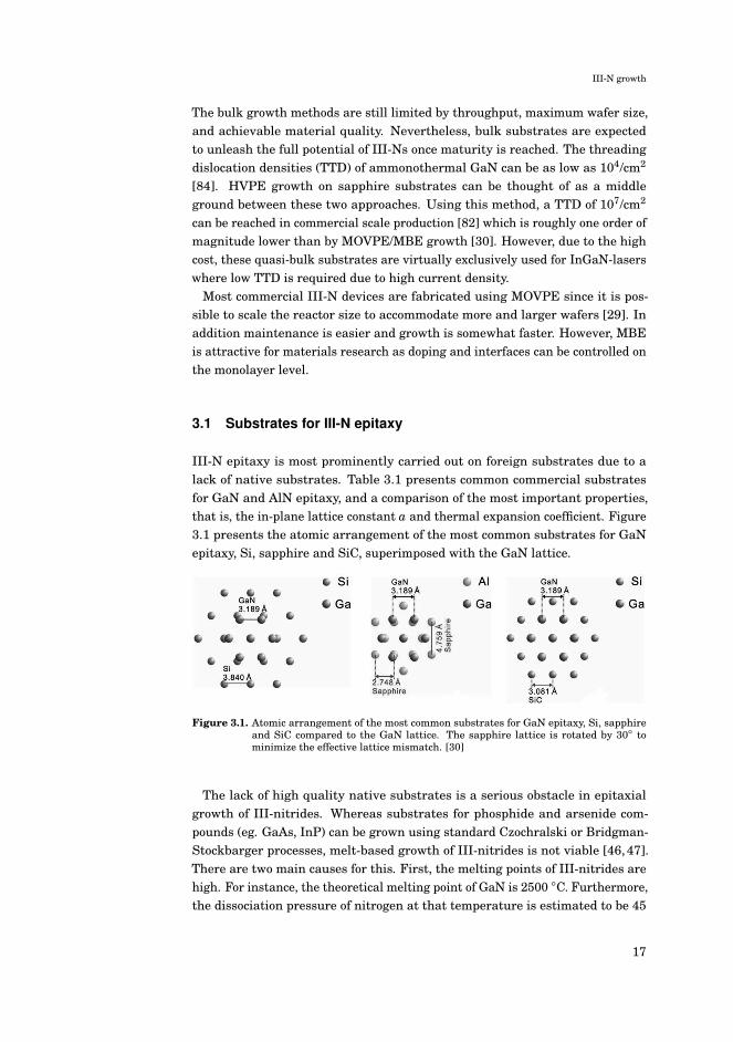
III-N epitaxy is most prominently carried out on foreign substrates due to alack of native substrates. Table 3.1 presents common commercial substratesfor GaN and AlN epitaxy, and a comparison of the most important properties,that is, the in-plane lattice constant a and thermal expansion coefficient. Figure3.1 presents the atomic arrangement of the most common substrates for GaNepitaxy, Si, sapphire and SiC, superimposed with the GaN lattice.
Figure 3.1. Atomic arrangement of the most common substrates for GaN epitaxy, Si, sapphireand SiC compared to the GaN lattice. The sapphire lattice is rotated by 30◦ tominimize the effective lattice mismatch. [30]
The lack of high quality native substrates is a serious obstacle in epitaxialgrowth of III-nitrides. Whereas substrates for phosphide and arsenide com-pounds (eg. GaAs, InP) can be grown using standard Czochralski or Bridgman-Stockbarger processes, melt-based growth of III-nitrides is not viable [46,47].There are two main causes for this. First, the melting points of III-nitrides arehigh. For instance, the theoretical melting point of GaN is 2500 ◦C. Furthermore,the dissociation pressure of nitrogen at that temperature is estimated to be 45
17

III-N growth
Table 3.1. Common substrates for III-N epitaxy and III-N materials [37].
Si (111) SiC Sapphire GaN AlN
In-plane lattice constanta nm
3.840 3.081 2.748 3.189 3.122
Lattice mismatch toGaN (%)
-16.95 3.54 16.09 - 2.47
Lattice mismatch to AlN(%)
-18.96 1.04 13.29 -2.41 -
Thermal expansion coef-ficient Δa/a (ppm/K)
2.6 4.2 7.2 5.6 4.2
Thermal expansion mis-match to GaN (%)
53 25 -28 - 25
Thermal expansion mis-match to AlN (%)
38 0 -71 -33 -
Thermal conductivity(W/cmK)
1.5 3.8 0.5 1.6 2.9
000 atm. Therefore, it is clear that GaN melt cannot be created at least withoutextreme conditions [45].
GaN is widely grown on non-native substrates despite the existence of nativeammonothermally grown and HVPE grown substrates. However, native sub-strates are not available in sufficient sizes and quantities at a competitive cost.Sapphire, Si and SiC are the most used substrates for epitaxial growth of GaNand typical substrate sizes range from 100 mm to 200 mm [30]. The use of thesesubstrates presents challenges especially in lattice mismatch, thermal expansionmismatch and, in the case of silicon, chemical stability [29, 30, 37, 68, 85]. Itis evident that the substrate choice is a compromise between factors such asprice and lattice mismatch together with electrical, chemical and mechanicalproperties. The use of non-native substrates has required the development ofdifferent nucleation and buffer layers in order to achieve high quality III-Nmaterial for devices.
It can be seen (Table 3.1) that SiC has the best properties for III-N growthout of the most common foreign substrates. SiC offers small lattice and thermalmismatches in addition to high thermal conductivity. SiC offers an almostlattice matched substrate particularly for AlN-based devices. However, SiC ismore expensive compared to Si and sapphire; therefore, SiC is mostly used forapplications in which high power density and material quality is preferred overunit-area cost, mostly RF power amplifiers [14,29,36]. SiC has a smaller in-planelattice constant, meaning that III-N layers can be grown under compression.This somewhat offsets the positive thermal expansion mismatch (SiC exhibitssmaller thermal expansion than III-Ns). When the grown structure is cooled toroom temperature, the III-Ns accumulate tensile strain. The strain due to these
18

III-N growth
mismatches needs to be balanced ensuring that the net effect is minimized in theintended storage and operating temperatures. Strain engineering is one of thekey components III-N epitaxy, as too high a strain can cause cracks renderingthe material unusable. Thin-films can withstand more compressive strain thantensile strain without forming cracks [86,87].
Sapphire substrate is considered to be one of the easiest substrates from thestandpoint of strain engineering, due to a positive lattice mismatch and negativethermal expansion mismatch [8]. Both factors allow the maintenance of thegrown film under compression. Table 3.1 uses effective lattice mismatch as theIII-Ns grown on sapphire have their lattice rotated by 30◦ around the c-axis tominimize the lattice mismatch. It should be noted that due to the relativelylarge lattice mismatch, III-Ns grown on sapphire quickly relax towards theirfree-standing lattice parameters. Furthermore, most commercial devices employpatterned substrates which enable control of the nucleation/coalescence, leadingto much lower TTDs, in addition to better light extraction from LEDs [8]. Thedownside of sapphire substrate is the low thermal conductivity which limitsachievable power density. However, sapphire is extensively used for blue/greenLEDs, where the optical transparency of sapphire is also a benefit.
GaN epitaxy on silicon is challenging due to lattice and thermal mismatches[29, 30]. In addition, GaN can not be grown directly on silicon since galliumreacts with silicon at elevated temperatures in a process called meltback etchingwhich renders the substrate and film unusable [29,30]. Despite these limitations,the growth of GaN on Si has high commercial potential since Si offers largesubstrates (currently up to 200 mm in (111) orientation) at a low cost. Si offersreasonable thermal conductivity which allows higher power density devices, suchas power electronics, in comparison to sapphire substrates. Furthermore, thereare many Si-compatible processing lines available in current fabs. AlthoughGaN-on-Si device processing is more difficult, for example, the Si substrate hasto be removed for LEDs due to Si absorbing much of the emitted light, the lowsurface area cost allows to offset the challenges for commercially viable products.Indeed, GaN-on-Si technology has found its way to LEDs, power electronics, andmicro-LED displays [8,36].
The development of a suitable buffer structure for GaN growth on Si has lastedsome time. The growth typically starts with AlN to protect the Si surface fromgallium. Then, AlGaN layers are deposited where the material composition ischanged from AlN to GaN. These layers are vital for strain engineering, theGaN layer has to be grown under compression due to large positive thermalexpansion mismatch [29,86,87]. The composition of the AlGaN layers can begraded step-wise, gradually, or in a chirped fashion. Different grading schemesallow a tailoring of the strain, dislocation annihilation, and possible interfacecharges [30].
The previously discussed substrates consists of only one material, althoughthe substrates can be patterned especially in the case of sapphire. One possiblecomposite substrate, a substrate consisting of multiple materials, is a silicon-
19

III-N growth
on-insulator (SOI) substrate. SOI substrates are readily available as they areused in the Si-CMOS industry and micro-electro-mechanical systems (MEMS).However, the (100) oriented Si is much more common than the (111) required forGaN epitaxy. A SOI substrate consists of a handle wafer which is typically (100)silicon, a buried oxide (BOX) which is SiO2, and a device silicon layer. Typically,the handle wafer also has a compensating oxide with the same thickness as theBOX to limit thermal expansion stresses. The use of a SOI substrate has beenshown to be beneficial for GaN epitaxy for two reasons. First, from the point ofepitaxy, the SOI substrate device layer together with the BOX can absorb someof the stresses generated during the crystal growth [88–92]. Therefore, lowerdislocation densities have been demonstrated using SOI substrates for GaNepitaxy. However, the use of a SOI substrate requires optimization of the bufferstructure to prevent cracks. Secondly, the BOX provides additional verticalelectrical insulation [91]. The vertical insulation of GaN-on-SOI was investigatedin Publication I. In its simplest form, this insulator decreases the vertical leakagecurrent, increases the vertical breakdown voltage and can reduce parasiticreactances in RF applications [34]. At the circuit level, the SOI substrate can beused to more efficiently isolate transistors when combined with trench isolation.A SOI substrate has been used to demonstrate monolithic integration of a half-bridge and gate driver logic [93,93]. The monolithic integration increases thelevel of integration which can be realized, and reduces the losses from gatedriver to power transistors. Although the use of a SOI substrate increases thecost of fabrication, the increased integration can reduce the total device costas packaging effort is reduced. This is a further testament to substrate choicebeing a vital part of the whole device and system design.
An extension of the composite substrates is the thermal expansion matchedsubstrate. In this substrate type, the substrate is constructed from multiple ma-terials in order to bring the total thermal expansion coefficient of the substrateclose to the epitaxial layers. In one approach, the substrate core is polycrys-talline AlN and the epitaxy-ready face is (111) Si [94]. This type of substrateoffers thermal expansion characteristics that are very close to that of GaN owingto the AlN core. The use of a thin silicon wafer as the surface allows largediameter substrates up to 8-inch. Using this approach, thick layers up to 15 μm(4-5 times than on typical Si-substrate) have been grown on 6-inch substrates[30, 94]. The layers show improved crystalline quality due to the increasedthickness and dislocation annihilation although the lattice mismatch betweenSi and GaN remains unchanged.
The vast majority of commercial III-N devices are grown as c-plane (0001)oriented GaN [8]. The reason for this is twofold. First, as mentioned, III-Nalloys preferably crystallize into a wurtzite lattice. In contrast, typical III-Vsemiconductors have a cubic lattice. Therefore, when using a conventionalIII-V substrate, it is challenging to realize an interface in which the atoms ofthe substrate and the epitaxial layer coincide. The atomic arrangement of thecrystal planes needs to have the same symmetry, and the difference in lattice
20

III-N growth
constants needs to be low for a mono-crystalline layer [80, 95]. For example,GaN grown on (100) oriented silicon leads to a multi-crystalline growth becausethe hexagonal GaN typically has four different orientations on the rectangularsilicon surface [68]. In contrast, similar GaN growth on (111) oriented siliconcan yield single crystal layers as both materials have a hexagonal symmetry inthe interface. Secondly, it seems that GaN requires delicate growth conditionswhen grown in orientations other than c-plane [62]. This is because the growthrate of GaN is dependent on crystal plane and, on the other hand, joininggrain boundaries with these planes can cause inversion domains and crystallinedefects [30, 61, 62]. Using a foreign substrate increases the creation of thesedefects. The annihilation of inversion domains and crystalline defects is moredifficult when GaN is grown in a non-polar or semi-polar orientation. Thesereasons clearly explain the extensive use of c-plane GaN in contrast to the otherorientations which present considerable challenges.
3.2 Metal-organic vapor phase epitaxy
Figure 3.2 schematically presents a simplified precursor delivery system in III-NMOVPE consisting of metal-organic and gas sources. A sophisticated gas controlsystem is required to efficiently control growth rate, material composition, andrealize sharp interfaces [80]. The purpose of this system is to achieve a suitableprecursor molar flow to the reactor, in addition to appropriately diluting andseparating the gas flows to limit parasitic reactions. In the MOVPE apparatus, acarrier gas, either hydrogen (H2) or nitrogen (N2), is used to transport and dilutethe source materials. There are many parallel gas lines so that the reactor flowcan be kept constant while switching between source materials. Furthermore,especially at the high temperatures required by III-N growth, there is a separatehigh flow rate of inert gas to overcome the effect of convection.
There are typically at least three different organo-metallic sources for group IIIatoms, trimethylgallium (TMGa), trimethylaluminum (TMAl) trimethylindium(TMIn) for Ga, Al and In, respectively. Triethylgallium (TEGa) is also commonlyused for low-temperature (In)GaN growth [8]. These precursor materials arebrought to the reactor in vapor form. The vapor is formed inside the sources,which are called bubblers. A carrier gas flows through the source and picksup some of the liquid precursor to form vapor. By controlling the bubblertemperature, pressure, and carrier flow rate, the precursor molar flow rate canbe controlled.
Ammonia (NH3) is typically used as the precursor for nitrogen. It should benoted that N2 is thermally too stable to be used as a source for atomic nitrogen.Other source materials for N, such as hydrazine (N2H4), have been used, butNH3 offers good reactivity and is available on an industrial scale. For n- andp-type doping, sources of silicon (Si) and magnesium (Mg) are used, respectively[70]. Typically, these sources are either silane (SiH4) or disilane (Si2H6) for Si
21

III-N growth
Figure 3.2. Schematic diagram of the gas lines of a MOVPE apparatus. Adapted from [96].
and bis-cyclopentadienyl-magnesium (Cp2Mg) for Mg. Carrier gases are notchemically active in the growth process; however, they do change the overallgrowth kinetics. N2 carrier gas is employed when growing In-containing alloyswhich are thermodynamically less stable and more prone to etching by H2 [8,97].
The precursor materials are brought to the reactor in vapor form by the carriergas. Figure 3.3 shows various transport processes and chemical reactions inthe MOVPE process [80]. Inside the reactor, the vapor comes into contact withthe heated substrate. The precursor in the vapor undergoes a reaction calledpyrolysis in which the atom of the desired material layer separates from theother atoms of the precursor molecule. With NH3, the molecule can be similarlythermally cracked to yield atomic nitrogen. The separated atoms then diffuseon the substrate where they can be incorporated to the semiconductor whilethe pyrolysis by-products are removed by the inert gas flow. However, some ofthe by-products are incorporated into the growing crystal. In MOVPE growth,the most common unintentional impurities are carbon, hydrogen and oxygen[67,71,98–100].
Some of the MOVPE reactors designed for III-N growth are cold-wall reactorsmeaning that only the susceptor is heated whereas other parts are cooled [101].The cold-wall design reduces parasitic reactions between the precursor materials,that is reactions that do not produce crystal growth but deposition on reactorwalls or other by-products. The reactors further employ liners, typically made ofquartz, that can be changed since there is some inadvertent deposition on thewalls. In addition, the liners reduce metal incorporation into the crystal from
22

III-N growth
Figure 3.3. Molecular transport and surface processes in a MOVPE reactor. Adapted fromReference [81].
the reactor metal parts. Another way to reduce the parasitic reactions is to mixthe group III precursors and ammonia just before the substrate. To achieve this,MOVPE apparatus can have two arrays of gas injectors, one for each precursortype, in close proximity to the substrate. The reactor in this work employs aclose coupled showerhead design in which the injectors are set to 11 mm fromthe substrate [101]. The susceptor is SiC-coated for thermal stability; othercoatings such as TaC, can offer even higher operating temperatures [66].
Growth in a MOVPE reactor is based on chemical reactions. The reactionproducing GaN can be simply described as
Ga(CH3)3(g)+NH3(g)→GaN(s)+3CH4(g). (3.1)
In this reaction, one TMGa molecule reacts with one ammonia molecule toproduce GaN and three methane molecules. However, the intermediate productsand reaction pathways are considerably more complex [8,102]. The molar flowof N into the reactor is typically orders of magnitude greater than the molar flowof group III atoms [8,20]. A higher molar flow, and thus partial pressure, of N isneeded since the dissociation pressure of N is much greater than for the groupIII atoms.
The temperature during growth is set to ensure that the grown material is ina metastable state, meaning that if the precursor flow is stopped, the crystalstarts to decompose [80]. For III-N materials, the growth temperatures are inexcess of 1000 ◦C [37,44]. The temperature is strongly dependent on the reactorpressure as at lower pressures the crystal is less thermally stable. Reducedpressures are typically used for III-N growth to reduce the parasitic prereactionsbetween the precursors. III-N growth is typically carried out in the metastableregime. In the metastable regime, the favorable lattice sites with higher binding
23

III-N growth
energies incorporate adatoms, whereas atoms trying to bind to lower energybinding sites can be desorbed [80]. Typically, lower growth rates produce bettermaterial quality as there is a higher probability of adatoms being desorbed fromlower energy defect sites. Similarly, impurity incorporation is reduced as theimpurity atoms in general have lower binding energies.
The majority of III-N growth is carried out in a mass transport limited temper-ature regime [35,37]. Here, the growth rate is limited by the gas phase transportof the precursors to the surface. The mass transport regime has a weak temper-ature dependence since the effects of gas density and diffusion constant limiteach other. Nevertheless, the desorption rate increases with temperature, andespecially H2 carrier gas can cause etching of the crystal surface.
3.3 Thermodynamics of crystal growth
Traditionally, when considering thermodynamics, three different growth modeshave been used to model epitaxy [80,95]. These are the Frank-van der Merwe(FM), Volmer-Weber (VW) and Stranski-Krastanov (SK) which are shown inFigure 3.4. These growth modes differ in the relative magnitudes of surface andinterface energies [80]. The FM mode can also be described as a layer-by-layermode. One full crystalline layer is completely grown before the next starts toform. In the FM growth, the binding energy between the substrate and theadatoms dominate compared to ad-atom to ad-atom binding. In contrast, theVW growth is characterized by 3D islands or aggregates, and in which the ad-atom interactions dominate. The islands can coalesce to produce a completelayer if growth is continued for a sufficiently long period. SK growth start asa thin-strained 2D layer known as the wetting layer. After a certain criticalthickness, 3D islands start to form. This implies that the relative strength of theinteractions change as a function of the film thickness due to the accumulatingstrain in the growing film.
III-N MOVPE growth displays some characteristics of FM and VW growthdepending on the substrate and thickness of the grown film. However, especiallythe multistep growth processes on sapphire are considerably more complex[104, 105]. The initial III-N growth on foreign substrates typically has VWcharacteristics, during which some islands or aggregates are formed. On onehand, this is due to the strain imposed by lattice mismatch, and on the other,the relatively low binding energies of the adatoms to typical substrates. Forexample, in GaN growth on sapphire, first, a low-temperature nucleation layeris deposited [8, 20]. Lower temperatures are used due to the low binding tothe substrate. Then, the temperature is increased to desorb and recrystallizeamorphous material into larger islands before continuing the growth at highertemperature. During higher temperature growth the islands grow and coalesceforming a 2D surface. After the coalescence, the growth exhibits layer-by-layercharacteristics.
24

III-N growth
Figure 3.4. Schematical cross-sectional view of growth modes in epitaxial growth: a) Frank-vander Merwe, b) Volmer-Weber and c) Stranski-Krastanov. Θ denotes the epitaxiallayer thickness in monolayers. [103]
Figure 3.5. Various atomic positions in the terrace-ledge-kink model.
3.4 Surface kinetics of crystal growth
Considering the surface kinetics, the substrate miscut should also be taken intoaccount as it creates preferred nucleation sites [80,95]. Miscut is the deviationof the substrate plane from the exact crystal orientation. A miscut substratehas a step-like surface morphology in which the step height ranges from oneto a few monolayers. Figure 3.5 presents schematically the surface of a miscutsubstrate and different atomic positions in a terrace-ledge-kink (TLK) model.The density of steps can be controlled by changing the miscut angle; a higherangle leads to more steps. The TLK model explains in a simplified form thedifferences in binding energy between lattice sites. Steps have a higher bindingenergy for adatoms as more bonds can be formed with neighbor atoms. Stepatoms, kink atoms, and step adatoms can form 4, 3, and 2 bonds in the TLKmodel, respectively, compared to a 1 bond of a terrace adatom. The increased
25

III-N growth
binding energy explains the preferred nucleation to a step edge compared to thestep terrace.
Figure 3.6. Step flow growth mode, island nucleation and roughening.
In an ideal case, nucleation would only occur on the step edges which incor-porate adatoms within the diffusion length with the steps then propagatinglaterally [106]. This growth mode is known as the step-flow growth, which isschematically presented in Figure 3.6. In practice, there might be some islandnucleation on the terraces due to spontaneous nucleation or nucleation to defectsites. The island nucleation needs to be sufficiently low to maintain step-flowcharacteristics and prevent surface roughening.
Island nucleation can occur on the terraces if the surface supersaturation, theamount of adatoms compared to desorbing atoms, is greater than the saturationneeded for spontaneous nucleation [106]. The supersaturation can be tuned by
26

III-N growth
changing various process parameters, such as the molar flow of the precursorsor temperature [99,100,106].
Figure 3.7. Step-bunching during step-flow growth.
Another phenomena called step-bunching, which is schematically presentedin Figure 3.7, can cause severe surface roughening during step-flow growth.In step-bunching, the lateral velocity of surface steps varies. The differencein velocities can lead to one step to catch another and form one higher step.The process is not self-limiting and can cause macroscopic step heights. Thebunching is caused by the difference in step-down or step-up adatom captureprobability to a step edge [107]. Step-bunching is more pronounced if the adatomdiffusion length is equal or greater than the terrace width. Therefore, substrateswith a greater miscut are more prone to exhibit step-bunching. Conversely,smaller miscut substrates have a wider growth parameter window for stablestep-flow growth.
3.5 N-polar III-N epitaxy
The vast majority of commercial III-N devices are grown using metal-polarc-plane orientation, although N-polar orientation could offer several benefits[8,35,108,109]. The lack of commercial devices based on N-polar III-Ns is dueto the challenges in crystal growth and resulting poor crystal quality [108].Especially high surface roughness of N-polar films has been a serious obstacle.N-polar epitaxy is more difficult than metal-polar due to different propertiesof these surfaces. Figure 3.8 presents the cross-sectional atomic structure ofmetal-polar (right) and nitrogen-polar (left) c-plane oriented III-Ns. N-polarsurfaces exhibit different diffusion energies and pathways [110–112]. Anotherchallenge is defining a stable single polarity film through nucleation layers[112,113].
N-polar GaN has been studied together with Ga-polar GaN since the start ofGaN research. In the early studies on sapphire substrates, it was found that thenucleation layer plays a critical role in defining the polarity of GaN [108,114,115].
27

III-N growth
Figure 3.8. Cross-sectional atomic structure of metal-polar (right) and nitrogen-polar (left) c-plane oriented III-Ns [108].
Typically, metal-polar GaN growth is started with a low-temperature (LT) GaNor AlN layer followed by desorption and recrystallization techniques. On theother hand, if the sapphire substrate surface is nitridated at a high temperature,the epitaxial layers are N-polar. The nitridation is followed by typical nucleationand recrystallization to reach a planar layer. Substrates with a miscut of 4◦
have been used to counter the formation of hexagonal hillocks [116].The atomic arrangement of a III-N surface, dangling bonds, and the most
favorable diffusion pathways depend on the material in question as well as thepolarity. For example, the theoretically thermodynamically stable surface forboth N-polar and Ga-polar GaN is Ga-terminated despite an N-terminated N-polar surface being possible under high nitrogen partial pressure [110]. However,for AlN, the Al-terminated (0001) and the N-terminated (0001) surfaces aremost stable for respective polarity [110]. N-polar films are typically grownusing higher temperatures and higher V/III-ratios (higher N-partial pressure) toachieve good crystalline quality [114,115,117–119]. Increasing the temperatureis most likely required due to the higher binding and diffusion energies of N-polar films [108]. On the other hand, the higher V/III- reduces the diffusion ofmetal-adatoms. In addition, too low a V/III-ratio can cause metal-polar domainsin N-polar growth, which was shown in Publication III.
There are two effects, hexagonal hillocks and step-bunching, which can causemacro-scale roughening of an N-polar surface, thus rendering the materialunusable for devices [112,116]. Step-bunching and hexagonal hillocks were ob-served in Publications III and IV. In early N-polar growth studies, the hexagonalhillocks were attributed to inversion domains, locations on the substrate atwhich the polarity of the grown material changes [113]. Later, the hexagonalhillock density was reduced by using a better substrate chemo-mechanicalpolishing and by using a miscut substrate [112, 113]. The hexagonal hillocksare independent of the substrate material and have been observed on nativesubstrates, Si, sapphire and SiC [113,116,118,120–124].
The remaining hexagonal hillocks, which are not due to inversion domains,
28

III-N growth
and step-bunching can be seen as manifestations of the same physical processes,although a rigorous model has not been established (Publication IV). The hillocksare predominantly generated during the nucleation of the epitaxial layer on thesubstrate, although unfavorable growth parameters can create a hillock at anypoint (Publication V). A substrate with significant miscut is frequently usedfor N-polar epitaxy to eliminate the hexagonal hillocks [116]. The miscut istypically between 2◦ and 4◦ for N-polar GaN growth. Increasing the substratemiscut increases the density of the surface steps. The surface steps are preferrednucleation sites as described in the TLK model. Increase in the step nucleationsites promotes step-flow growth and reduces the adatom supersaturation onthe terraces, thereby reducing island nucleation. These factors significantlyreduce the hexagonal hillock growth. However, the use of a miscut substrate cancause step-bunching [116]. The probability of step-bunching increases when thesurface step separation compared to the diffusion length is decreased. On theother hand, it seems that N-polar surfaces have different relative probabilitiesbetween the step-up and step-down capture than metal-polar ones [106, 107].The elimination of hexagonal hillocks was demonstrated in Publication IV.
The hexagonal hillocks can be also eliminated by tuning the process parame-ters, which was demonstrated in Publication IV. This is especially important forN-polar AlN which is very prone to step-bunching. It has been shown that thehexagonal hillocks can be eliminated by using a high growth temperature, lowgrowth rate and high V/III-ratio, even when using nominally on-axis substrates(Publications IV and V). The high temperature and low growth rate both reducethe surface supersaturation and island nucleation [106]. On the other hand,increasing the V/III-ratio decreases the diffusion length, thus reducing thecapture of adatoms into an island nucleus and step-up capture onto the plateauof a hillock [125]. It could be possible that a very high N partial pressurechanges the relative probability of the step-up and step-down capture rates[107]. However, it is difficult to separate the contributions of these differentprocesses to hillock generation and further studies are needed.
SiC is a good substrate for studying the polarity of III-Ns since the SiC surfacetermination, also referred to as carbon- or silicon-face, defines the preferentialpolarity of the epitaxial layer [126,127]. The polarity of grown AlN films wasinvestigated in Publication III. Metal-polar films are obtained on silicon-face SiCand, in contrast, carbon-face SiC yields N-polar material [127]. However, mixed-polarity films can result if the growth parameters are too far from the optimalgrowth window for certain polarity. For example, too low a growth temperatureor V/III-ratio causes mixed polarity AlN on carbon-face SiC. Generally, metal-polar growth is considered more stable in retaining a set polarity. In mostcases, the growth of GaN on SiC starts with an AlN nucleation layer since theadhesion of Ga to SiC is low. It is possible to directly grow GaN on SiC at areduced growth temperature [128]. In addition, the AlN can be used for strainengineering and to offer some lattice mismatch mitigation. As N-polar III-Nsrequire elevated growth temperature, N-polar growth of GaN on SiC necessitates
29

III-N growth
the use of AlN nucleation layer. A substrate with high miscut (∼ 4◦) is used toeliminate hexagonal hillocks. The AlN layer thickness is kept low, some tensof nanometers, as N-polar AlN is very prone to step-bunching and the surfaceroughness increases quickly as thickness increases [129]. The nucleation layeris planarized using a low-temperature GaN or AlGaN layer [129]. Then, themain GaN layer, with a resistive interlayer, and the active layers are deposited[130,131]. It has been recently shown that arbitrarily thick N-polar AlN withouthexagonal hillocks or step-bunching can be obtained on substrates with a miscutof 1◦ or less (Publications IV and V). These AlN layers can be used for devicesbased on either AlN or high Al-content AlGaN. It should be also possible to usethese layers for N-polar GaN.
N-polar layers can be obtained on (111) silicon substrates by polarity inversion[124]. The growth process is very similar to metal-polar GaN growth, the growthstarts as metal polar. However, a greater substrate miscut (∼ 4◦) has been used toreduce the amount of hexagonal hillocks. First, an AlN nucleation layer or layersare deposited followed by the AlGaN layers for strain engineering. During theAlGaN layers, polarization inversion is generated by using high concentrationmagnesium-doping [124]. The alloy grading and doping allows the achievementof stable polarity inversion and the following layers are N-polar. A thick andresistive GaN buffer layer is required for device vertical insulation due to theMg-doped GaN being conductive. Finally, the device layers are grown on top ofthe GaN buffer. It might be possible to directly grow N-polar layers on silicon ifan N-polar AlN layer can be nucleated through some surface conditioning.
30

4. Characterization methods
A variety of characterization methods are required in order to account for themultiple physical properties that are vital for III-N devices [8, 35, 132]. Theproperties of interest include layer thickness, alloy composition, material dis-order and surface/interface roughness. The very first characterization occursduring crystal growth through in-situ monitoring. Typical characterization meth-ods can be divided into beam-based (scanning electron microscope and X-raydiffraction) and contact methods (atomic force microscope and selective etch-ing). Another division can be formed between destructive and non-destructivemethods. The selective etching is consider destructive as typically the sampleis consumed in the process while the other methods presented in this disserta-tion are non-destructive, the sample can be processed further into devices aftercharacterization. Many measurement setups can complement each other, espe-cially in cases in which a quantitative figure of merit is a function of multiplemeasurands. For example, converting the bulk density of charge carriers intosheet density requires knowing the layer thickness.
4.1 In-situ monitoring
In-situ monitoring in the context of this thesis refers to the measurementsthat are conducted during crystal growth inside a MOVPE reactor. In-situmonitoring is a tool for optimizing and monitoring the growth typically in termsof growth rate (layer thickness), surface roughness and strain [133]. Further,active process control can be utilized when the reactor parameters are tunedafter a certain point (e.g., thickness) is met, which is especially effective duringprocess development. Since the layers are measured as they form, some of theproperties can be extracted more easily than when working on the completelayer stack. For example, the change in the surface roughness can be more easilytraced to a certain layer or growth step.
The vast majority of in-situ monitoring is optically performed through view-ports in the reactor showerhead. Multiple spots along a wafer can be measuredas the wafer is rotated in the reactor. Modern III-N reactors typically offer three
31

Characterization methods
different types of in-situ measurements. These are reflectance, temperature,and substrate curvature. The reflectance is mainly used to assess the layerthickness and roughness. The reactor used in this dissertation provides threedifferent wavelengths for the reflectance measurements, 405 nm, 633 nm and950 nm [101, 133]. A shorter wavelength offers better resolution both for thelayer thickness and roughness, but can be absorbed depending on the materialbeing grown. The reflectance measurement is schematically presented in Figure4.1 on the left. A laser beam is aligned through a view port of the reactorshowerhead. The beam is reflected back by a substrate and is collected into adetector using a beam splitter.
�
Figure 4.1. Reflectance measurement and emissivity corrected temperature measurement leftand right, respectively.
An accurate temperature reading on the sample surface is important for pro-cess repeatability and development as there is a significant difference betweenthe reactor heater temperature and the substrate surface temperature. Fur-thermore, the difference changes depending on the growth conditions and wafercurvature. Two instruments provide complementary data for measuring thetemperature. The first is the emissivity-corrected substrate surface temperaturemeasurement which is presented in Figure 4.1 on the right. The emissivity ismeasured by directing a broad band light source to the substrate and measuringthe sample reflection coefficient. It should be noted that the film stack emissivitychanges while the material is grown. The temperature is estimated by fittingthe sample black-body radiation which is corrected by the measured sampleemissivity.
32

Characterization methods
The second temperature measurement setup is the mapping substrate surfacetemperature measurement which is shown in Figure 4.2 on the left. The temper-ature profile is important for achieving uniform layers as the growth rate andespecially the composition of In-containing alloys is dependent on the surfacetemperature [97,134]. Due to the complexity of the emissivity correction, thetemperature profile is a more qualitative tool to reduce relative temperaturedifferences by adjusting the reactor heaters. The temperature profile is mea-sured by a two-wavelength array of diodes which have a different sensitivityto infra-red radiation. The whole wafer can be mapped as it is rotated in thereactor. The relative intensities are used together with a fitting to a black-bodymodel for the temperature estimates.
Figure 4.2. Mapping temperature measurement and substrate wafer curvature measurementleft and right, respectively.
The wafer curvature measurement is presented in Figure 4.2 on the right.The wafer curvature is monitored to realize crack-free layers and wafers whichare sufficiently flat for device processing. These considerations are especiallyimportant for GaN-on-Si epitaxy due to the large lattice and thermal mismatches,which become more prominent as the wafer size is scaled up [30]. The thermalexpansion effects can be estimated as the bare wafer is heated up to growthtemperature and, conversely, when the complete layer stack is cooled after theprocess. The strain state of grown films can be assessed by observing the changein wafer curvature during layer growth [135]. For example, a perfectly latticematched film should not alter the wafer curvature during growth. The wafercurvature is measured by aligning two parallel 405 nm laser beams through aview-port perpendicular to the wafer. The reflected beams are guided back intoa detector. The curvature can be estimated by comparing the change betweenthe distance of the laser beam spots on the detector.
33

Characterization methods
4.2 Atomic force microscope
Figure 4.3. Atomic force microscope setup and effect of tip convolution to measured samplemorphology a) and b), respectively.
An atomic force microscope (AFM) is a physical contact microscope for measur-ing the surface morphology of a surface down to atomic resolution in an idealcase [132]. The advantage of AFM over most microscopy techniques is that it cangive quantitative results such as the surface height as a function of location. TheAFM is based on the atomic forces, which can be either attractive or repulsivedepending on the distance, between an atomically sharp tip and the sample.
The most used measurement for thin-films is the semi-contact mode. Figure4.3 a) presents the AFM measurement setup. In this measurement mode, thetip is attached to a cantilever which is set to vibrate at a certain frequency.The frequency is measured by directing a laser beam to the tip and collectingthe reflected beam to a detector. As the tip is brought into close proximityto the sample, the force between the tip and the sample alters the vibrationfrequency. The cantilever is moved up or down with piezoelectric actuatorsto maintain the nominal vibration frequency. The sample surface height at a
34

Characterization methods
certain location can be collected from the actuator movement. The cantilever ismoved to scan the sample surface to collect the surface morphology. Due to thephysical nature of the measurement, the measured surface is the convolution ofthe actual surface and the tip properties. Figure 4.3 b) presents the effects oftip convolution. The tip convolution is small for samples in which the aspect-ratio of structures is low, that is, the height changes are small compared to thelateral scale. Conversely, AFM might not reproduce high-aspect ratio structurescorrectly whereas undercut features cannot be measured at all.
4.3 Scanning electron microscope
A scanning electron microscope (SEM) is a beam-based microscope which allowsthe observation of much smaller features than an optical microscope on a rel-atively large lateral scale (some millimeters) [132]. This higher resolution isdue to the smaller wavelength of high energy electrons compared to visible light.An electron with an energy of 10 keV has a wavelength of approximately 10 pm[132]. On the other hand, the optical microscope is typically diffraction-limitedwhen imaging microfabricated structures. The features that can be accuratelyobserved in optical microscope are in the order of visible light, roughly 500 nm,whereas a SEM allows one to observe structures down to the nanometer-scale.
Figure 4.4. Scanning electron microscope setup [136]
The SEM operates by focusing an electron beam to the sample surface. Thebeam is generated by an electron gun with it being shaped and deflected byelectro-magnetic lenses. Two types of electrons are emitted by the samplewhen being illuminated by the electron beam. These are the backscatteredand secondary electrons. The backscattered electrons are caused by elastic
35

Characterization methods
scattering of the electron beam and the specimen atoms. Heavy elements causemore backscattering, which generates some contrast between different materials.Secondary electrons are emitted when the beam electron ejects an electron froma sample atom. By scanning the sample with the beam, the emission intensityas a function of location is measured to produce a grayscale image. The contrastin the image is produced by the change of emission intensity due to differentmaterials and features. SEM can only yield quantitative results in the lateralplane, it is possible to laterally estimate the distance between two features,but not the difference in height. Further, some information on the samplemorphology is needed to correctly interpret the images. Elemental analysis canbe performed to some accuracy by measuring characteristic X-rays generatedin the sample. The characteristic X-rays are generated when an electron in thesample atom is ejected and the vacancy is filled by a higher energy electron.The electron transition energy is released in the form of an X-ray photon whoseenergy is characteristic to the element in question.
4.4 Selective etching
Selective etching is a destructive characterization method that is applied togain a direct assessment of certain material parameters especially during thefirst steps of process development or in order to calibrate non-destructive andindirect characterization methods. Selective etching is used to enlarge smallfeatures to enable them to be viewed using other characterization methods orto increase the difference between two materials that are otherwise difficult todistinguish [137–140].
An example of the first case is defect selective etching (DSE). DSE is appliedto provide a direct estimate of the threading dislocation density of a thin-film[137, 138]. The threading dislocation cores that reach the film surface aretypically very small, therefore making it difficult to map them using microscopy,such as SEM or AFM. DSE increases the core size by creating an etch pitto render it visible in microscopy. DSE is particularly effective in measuringlow defect density samples or samples in which the spatial defect density isnon-uniform, such as films grown on patterned substrates. In these cases, thecommonly used X-ray diffraction (XRD) needs elaborate modeling to correctlyestimate the defect density [75,141]. DSE provides a direct defect density valuewhich could then be used to calibrate the XRD measurements for the particularepitaxy process.
DSE is based on the different etch rates of the dislocations on the crystalsurface. The difference is due to the varying chemical reactivity of crystalplanes and material composition variance near a dislocation. Typical etchantsinclude heated H3PO4, KOH and eutectic KOH-NaOH [137–140]. Etchingenvironment and parameters need to be chosen to ensure that all the dislocationsare sufficiently enlarged to be visible but not overlapping due to overetching.
36

Characterization methods
DSE of GaN allows a determination of whether the dislocation in question isan edge, screw, or mixed dislocation. It has been shown that the etch pit size issmallest for edge dislocations followed by mixed and screw dislocations [142].The size is in contradiction with the dislocation burgers vectors in which edgedislocation has the smallest size followed by screw and mixed dislocations. Thedifference has been attributed to varying impurity incorporation between thedislocation types [142].
Selective etching is an effective and simple method to find the polarity ofa c-axis III-N film [139, 140]. It has been shown that a metal-polar film isunaffected by an aqueous KOH solution whereas an N-polar film is readilyetched [139,140]. The difference in chemical reactivity between the polarities isdue to surface termination and the number of dangling bonds [110,111]. Thepolarity of a sample or possible polarity inversion domains can be studied bythe polarity-selective KOH etching and imaging the sample with SEM after theetch.
4.5 X-ray diffraction
X-ray diffraction (XRD) is a powerful and important non-destructive tool forcharacterizing crystalline quality and interfaces of epitaxial layers or stacks oflayers. XRD can be used to study the crystal orientation, estimate dislocationdensities, strain, stress, alloy composition and whether a layer is strained orrelaxed [75,141]. XRD probes the collective properties of a certain volume of thecrystal and yields quantitative values, such as peak widths or lattice constants,as opposed to other methods, such as microscopy, which allows, for example,individual dislocations to be qualitatively observed. The quantities provided byXRD analysis can be related physical properties including dislocation density,lattice constants and strain. Typically, the beam area is between 10 mm × 10 mmand 1 mm × 1 mm and the probed material depth some tens of micrometers.
Figure 4.5. Geometrical representation of Bragg’s law.
XRD is based on the interaction between X-ray photons and the electron cloudsof the atoms in the studied material. The distance between atoms in crystalline
37

Characterization methods
solids is roughly on the same order of magnitude as the wavelength of X-rayphotons, 0.1 nm, which enables diffraction. The crystal can be seen as a 3Ddiffraction grating. Each atom in the crystal can be thought of as a source ofspherical waves. The atomic arrangement in the crystal determines the angles ofdiffraction, and the elements determine the diffraction intensity. The differencein distance traveled, and thus, the phase between the waves, causes constructiveinterference according to Bragg’s law
nλ= 2dsinθ, (4.1)
where n, λ, d, and θ are the order of diffraction, wavelength, distance betweenthe lattice planes and angle of diffraction, respectively. The Bragg’s law geomet-rically is presented in Figure 4.5. The order of diffraction is typically chosento be one for better resolution. This can be achieved by using specific sets orsubsets of lattice planes. For a hexagonal lattice, such as the III-Ns, the latticespacing is given by
d =√
3
4( h2+k2+hka2 + 3l2
4c2 ), (4.2)
where h, k and l are the Miller indices of the plane and a and c are the latticeconstants.
4.5.1 High-resolution X-ray diffraction setup
Figure 4.6 schematically presents a typical high-resolution XRD (HRXRD) setup.The X-ray source for material studies typically has a copper anode inside avacuum tube which is bombarded by high energy electrons. When the electronshit the anode, wide spectrum Bremsstrahlung (deceleration radiation) andcharacteristic X-rays are produced [141]. The characteristic X-rays are createdwhen a high-energy electron knocks an inner-bound electron from orbit in theanode material. The vacant energy level is filled by a higher energy boundelectron and the energy difference is emitted as an X-ray photon. CharacteristicX-rays are useful for diffraction studies, because the energy spectrum, andin turn, the wavelength spectrum, is narrow in addition to the high intensity.Copper is chosen due to it possessing a suitable emission line Kα1 with awavelength λ = 0.1540560 nm [75], in addition to good thermal stability andconductivity. Thermal conductivity is important for the X-ray tube operationsince the X-ray generation efficiency is about 1%.
The X-ray beam exiting the source is divergent with a parabolic mirror beingused to collimate the beam. The HRXRD setup uses two monochromatorsto increase the angular and wavelength resolution needed for highly orderedepitaxial materials. The resolution is increased because Bragg’s condition issatisfied at a smaller angle range. A monochromator ideally selects only asingle wavelength corresponding to a suitable emission line and angle of thebeam. The monochromator is based on quadruple diffraction from nearly perfectgermanium crystals. The first monochromator is located after the source and
38

Characterization methods
Figure 4.6. Schematic diagram of high resolution XRD setup [59].
before the sample. The angle between the sample surface and the incident beamis called ω. The sample stage can be rotated around multiple axes in order toreach a suitable diffraction. The sample diffracts the beam into multiple exitingbeams. The angle between the incident beam and a diffracted beam is called2θ. In a symmetrical measurement, ω= 2θ/2. The diffracted beam is directed toa detector through an analyzer crystal, which again has a narrow wavelengthand angular acceptance. The analyzer crystal further increases resolution andselects only the diffraction due to elastic scattering in which the energy and, inturn, wavelength, is conserved.
The downside of using the full HRXRD setup is that for high angular resolutionmuch of the beam intensity is sacrificed. Therefore, the detection limit in termsof combined material thickness and quality is reduced compared to the powderXRD setup; in other words, the measurements are slower, especially for thinneror lower quality films. The setup choice is a compromise between time andprecision. One way to significantly speed up the measurement is to use andetector array. In this approach, which uses a CCD array, the detector cansimultaneously sample photons on multiple angle values. Some measurements,such as reciprocal space mapping which is discussed later, require an orderof magnitude less time when using a CCD detector, although at a reducedangular resolution, due to the lack of an analyzer crystal. Nevertheless, thearray detector setup is sufficient for the vast majority of epitaxial III-N films.The full HRXRD setup is required if the crystal under consideration is grownusing bulk methods, absolute lattice constants are being studied (as opposed to,e.g., relative location to the substrate peak) or there are partially overlappingpeaks as can be the case with AlN and SiC due to a small lattice mismatch.
39

Characterization methods
4.5.2 Reciprocal space
Reciprocal space is a convenient mathematical tool for analyzing XRD of crys-talline solids. The definition of reciprocal space allows a connection between themeasured peak positions to in-plane and out-of-plane lattice constants and peakbroadening into physical properties. Reciprocal lattice can be constructed fromthe basis vectors of three dimensional lattice. If the direct space lattice vectorsare a1,a2 and a3, the reciprocal space vectors are defined as
b1 = a2 ×a3
a1 ·a2 ×a3,
b2 = a1 ×a3
a1 ·a2 ×a3and (4.3)
b3 = a1 ×a2
a1 ·a2 ×a3.
The cross product in 4.3 causes the reciprocal lattice vectors to be perpendicularto the respective real space vectors. In other words, a reciprocal space vectoris perpendicular to a plane span by real space vectors. A vector Hhkl drawnin the reciprocal space from the origin to coordinates (h,k,l) is perpendicularto the real space lattice plane with Miller indices (hkl). The denominator inthe equations 4.3 equals the volume of the real space unit cell and thus thevolume of the reciprocal space unit cell is the inverse of a real space unit cell.Similarly it follows that the length of reciprocal space vector Hhkl , which is alsoknown as the scattering vector, is connected to the real space lattice spacingdhkl as |Hhkl | = 1/dhkl . The reciprocal space vector Hhkl can be described usingthe incident and diffracted beam wave vectors, Hhkl = k0 - ks, which allows thetransformation of measured quantities to a reciprocal space.
The reciprocal space is typically expressed in terms of two components Qx andQy, which are on the same plane as the incident and diffracted wave vectors k0
and ks. Qx and Qy correspond to direction parallel to a certain real space planewith Miller indexes (h,k,l) and direction perpendicular to the plane, respectively.The magnitude of Qx and Qy can be calculated from the measurement geometryusing the angles between the sample and the incident and diffracted beams
|Qx| = 12
(cos(ω)− cos(2θ−ω)) and (4.4)
|Qy| = 12
(sin(ω)+ sin(2θ−ω)). (4.5)
40

Characterization methods
4.5.3 Measurement types and geometries
��
Figure 4.7. Schematic example of reciprocal space mapping around an off-axis reflection. Sub-strate and four different cases are presented. Lattice matched, relaxed, tenselystrained, and partially compressively strained layer cases (a, b, c, and d, respectively)are shown.
There are two typical one-dimensional measurements for characterizing crys-talline semiconductors. These are the ω and the ω−2θ scans. In the ω scan,the sample stage is typically rotated such that the ω angle changes but the 2θangle stays constant. Other measurement setup geometries are also possiblethat are equivalent from a diffraction point of view. In reciprocal space, the ω
41

Characterization methods
scan traces an arch around the origin. In other words, the scattering vectorlength is maintained but the direction is changed. This can be seen as probinglattice planes with the same spacing but different orientation. Peak broadeningin an ω scan can be connected to material disorder, non-homogeneous strain anddislocations [75]. On the other hand, in an ω−2θ scan, the difference between ω
and 2θ is maintained such that ω−2θ/2 is constant. In this case, the scatteringvector length changes, but the orientation remains constant. This means thatlattice planes with the same orientation but different spacing are probed. Whenmeasuring epitaxial stacks, different peaks around certain reciprocal latticepoint in the ω−2θ scan are typically created by different materials.
Most common measurement geometries can be divided into three categories,symmetrical, asymmetrical, and skew-symmetric. In the symmetrical case, theincident and diffracted beam angle are equal ω= 2θ/2, which is opposite to theasymmetrical case where ω �= 2θ/2. In the skew-symmetric case, ω= 2θ/2 but thediffraction plane (span by k0 and ks) is not perpendicular to the sample surfaceinstead the sample is tilted along χ-axis. Symmetrical scans probe planes (0,0,l),l ∈N+. Asymmetrical and skew-symmetric scans can be used to probe off-axisplanes (h,k, l) where either h or k �= 0 and l ∈N+. The geometry for arbitrarylattice plane can be found using the lattice plane spacing in Equation 4.2 andBragg’s law (Equation 4.1). For off-axis planes, basic geometry can be used tocalculate the angle between the sample surface and the desired lattice plane.This angle is then used to offset the ω and 2θ in asymmetrical scans or as theχ value in skew-symmetric scans. For the asymmetrical scans, it is beneficialto use a geometry where the ω angle is greater. This geometry creates beamcompression and reduces measurement time compared to the opposite case ofbeam broadening.
The symmetrical scans can be used to obtain the out-of-plane lattice constant cand estimate screw or mixed type dislocation densities based on peak broadening.Symmetrical scans do not provide information on pure edge-type dislocationssince the edge dislocation Burgers vector (direction and magnitude of the dislo-cation) and line direction are perpendicular to the diffraction plane [75]. Thiscan be checked with the invisibility criterion
g · (b×u)= 0 (4.6)
where g,b and u are the reflection, Burgers vector and dislocation line direction.Similarly, symmetrical scans do not offer information on the lattice parameter asince the (0,0,1) and (1,0,0) planes are orthogonal. Analogously, it can be seenbased on Equation 4.4 that Qx = 0 if ω= 2θ/2.
To access the lattice parameter a and reciprocal space coordinate Qx asymmet-rical scans can be employed for of-axis reflections. Especially reciprocal spacemaps (RSM) around these reflections are useful for determining the strain/re-laxation state of heterostructures. A RSM is a 2D slice of the reciprocal spacearound a certain reflection. Figure 4.7 schematically presents a RSM around anoff-axis reflection. Strained epitaxial layers share the same lattice constant a;
42

Characterization methods
therefore, the peaks exist on the same Qx coordinate (Figure 4.7 a. Converselya relaxed layer (Figure 4.7 b exhibits the lattice constants of an unstrainedcrystal. Although the layer is strained, it might not be lattice matched andthe Qy coordinate (connected to lattice parameter c) is important to assess thestrain state. A tensile (compressive) in-plane film stress causes out-of-planecontraction (expansion) compared to the relaxed value according to the Poissoneffect (Figure 4.7 c and d). Furthermore, both lattice constants are requiredwhen determining the alloy composition of a (partially or fully) strained layer.While the asymmetrical RSMs are typically used for overview of the epitaxiallayer, the asymmetrical scans similar to the symmetrical scans do not offerinformation on the edge dislocation density.
skew-symmetric scans are able to assess the edge dislocation density as thedislocation line direction does not coincide with the diffraction plane. Further-more, these scans can access more reflections since the sample does not blockthe beam. The contribution from edge dislocations to peak broadening increasesas the χ-angle increases and the diffraction plane moves closer to being per-pendicular to the edge dislocation line direction. Conversely, the contributionfrom screw dislocations to peak broadening is reduced. The downside of using askew-symmetric configuration is that the diffraction intensity is reduced, whichcan increase the required measurement time or render measurements infeasiblewith lower quality or thinner samples [75].
4.5.4 Threading dislocation density
The mosaic model is typically used to approximate the disorder in epitaxialIII-Ns [75,76]. The model approximates a highly disordered film reasonably well.The total threading dislocation density in III-N epitaxy on foreign substratesis typically in the order of 108/cm2 or greater. For bulk III-Ns or heteroepitaxy,other models are required. In addition, it could be beneficial to use topographyin order to analyze individual dislocations [143–146].
In the mosaic model, the crystal consist of grains that are themselves perfectlyordered but are slightly misoriented from each other. The misorientation be-tween the grains is split into two orthogonal components, tilt and twist. Tilt andtwist describe the grain alignment away from the substrate normal and rotationaround the substrate normal, respectively. Tilt creates screw dislocations on thegrain boundaries while twist causes edge dislocations. A dislocation that hascontribution from both tilt and twist is called a mixed dislocation.
The diffraction from the crystal is constructed from the contributions of indi-vidual grains. Each of the grains produces a narrow diffraction peak. The peakspoint in slightly different directions depending on the order of misorientation.Collectively, the diffraction peak resembles either a Gaussian or a Lorentzianlineshape. It can be shown that for the mosaic model the dislocation density isdirectly proportional to the peak broadening and inversely proportional to thegrain size. However, for randomly distributed dislocations the peak broadening
43

Characterization methods
is directly proportional to the square of the dislocation density. For high dis-location density, the two approaches yield roughly the same estimates as thedistance between dislocations is small; hence, it is typically easier to assumethe random distribution [75]. Low dislocation films require more sophisticatedmethods [75].
The total dislocation density can be estimated by separating the contributionsof tilt and twist to peak broadening. The symmetrical reflections peak widthis only affected mostly by the screw dislocations with some broadening due tomixed dislocations. Similarly, the edge dislocations cause most of the broadeningof an in-plane peak together with some components from mixed dislocations.However, it is difficult to measure in-plane scattering; therefore, a series ofskew-symmetric scans with different χ-angle are used. The contributions fromtilt and twist can be separated using the following relation:
β2hkl = (βtilt cosχ)2 + (βtwistsinχ)2 (4.7)
where βhkl , βtilt, βtwist and χ are the measured width of a diffraction peak withMiller indices (hkl), peak broadening due to crystalline tilt, peak broadeningdue to crystalline twist and measurement inclination angle for the diffractionpeak with Miller indices (hkl). Based on Equation 4.7, it can be seen that thepeak broadening in low (high) χ-angles is mostly from tilt (twist). Since typicallythe edge dislocation (twist) density in epitaxial III-N is greater by an order ofmagnitude, high χ-angle scans offer better view of the overall crystal quality.
In highly disordered films, the aforementioned approach can be justified as thedislocations typically dominate the peak broadening. Other factors can becomesignificant, especially in low dislocation density films, in bulk crystals, crystalsunder high strain, or in curved structures.
4.6 Synchrotron X-ray topography
Synchrotron X-ray topography (SR-XRT) utilizes the broad and continuous elec-tromagnetic spectrum generated by the synchrotron beam bending magnets[143–145,147]. SR-XRT allows the observation of individual features, such asdislocations, as opposed to the collective crystal properties. SR-XRT is mostsuited for near perfect crystals with dislocation density in the order of 106/cm2 orlower. In high disorder materials, the contributions from individual dislocationsoverlap in the topograph. The synchrotron radiation is a secondary effect ofthe particle accelerator which was found to be useful for studying the structureof crystalline solids. Currently, some synchrotrons are dedicated for the syn-chrotron radiation studies. The continuous, high brilliance and low divergencebeam, especially in the X-ray spectrum, is effective for characterizing crystallinesemiconductors.
The synchrotron radiation is generated as electrons travel in a semi-continuousmanner in a circle. The electrons are guided with bending magnets. The change
44

Characterization methods
of electron momentum in the magnet causes the emission of continuous X-rayradiation. The X-ray wavelength is in the 0.1 nm range, which is in the sameorder as the lattice constants in crystalline solids, thus enabling diffraction.
The broad X-ray spectrum allows the simultaneous recording of multiplediffractions as Bragg’s condition is satisfied by multiple lattice planes [143–146].The X-ray beam is directed on the sample and the resulting diffraction patternis recorded on X-ray film. A perfect crystal would produce a uniform diffractionintensity. Any deviation from a perfect lattice, such as dislocations, grainboundaries or strain, causes deformation of the diffracting lattice planes andthus results in a non-homogenous diffracted intensity [143–146]. The sample istypically tilted by few degrees allowing symmetrical reflections to be recorded.Otherwise, the symmetrical reflections are lost in the pattern generated by thebeam.
Two measurement geometries are used, back reflection and transmissiontopographs. In back reflection, the X-ray beam passes through the X-ray filmbefore reflecting (diffracting) back from the sample. The back reflection is mostsensitive to the material on the sample surface. Conversely, in the transmissiongeometry, the beam travels through the sample before being collected on thefilm. The transmission topography probes the bulk of the crystal.
45


5. III-N field effect transistors
III-N field effect transistors (FETs), especially high electron mobility transistors(HEMTs), offer superior performance compared to other semiconductor materialsystems for high-power density and high-frequency applications [13,14,31,35,36].This is mainly due to the high band gap and resulting high breakdown field inaddition to the ability to create a transistor channel that has a high densityof charge carriers with high mobility and saturation velocity. This channel istypically described as two-dimensional-electron gas (2DEG) with the deviceswith this channel type being called HEMTs. HEMTs exhibit a high attainablecurrent density and high operation frequency due to the low resistance and highmobility of the 2DEG. HEMTs are the most common III-N transistors, althoughdevices with doped channels exist [148]. However, the doped III-N FETs facechallenges in dopant activation due to the high band gaps of these materialsand reduced charge carrier mobility due to scattering.
The first HEMT demonstration was based on an AlGaAs/GaAs heterostructurein 1980 [15]. The GaAs HEMTs saw quick adoption as RF amplifiers wherethey started to replace GaAs based metal-semiconductor field-effect transistors(MESFETs) which had been developed during the 1970s [12]. A commercialGaAs HEMT amplifier was already launched in 1983 [16]. The III-N HEMTswere delayed by the available material quality. Most of the material issues weresolved in the late 1980s and early 1990s during the race for an efficient blueLED [8, 20]. By leveraging the developed growth techniques, an AlGaN/GaNHEMT was finally demonstrated in 1993 [24]. The HEMTs in commercial RFapplications are especially seen in the form of monolithic microwave integratedcircuits (MMIC) where they have seen use in cell phones and other telecom-munication systems and radars [13, 14]. At present, the GaAs-based HEMTsare targeted at applications which require extreme frequencies as these deviceshave demonstrated cut-off frequencies in excess of 1 Thz, which is a result ofthe remarkable electron mobility [13,57]. On the other hand, GaN MMICs arepoised to take over many applications under 100 GHz as they have shown ordersof magnitude higher output power owing to the large GaN breakdown field [14].Another application field for the GaN HEMTs is power electronics [31,36]. Here,the high breakdown field together with low on-resistance and high oscillation
47

III-N field effect transistors
frequency allows the construction of very efficient circuits. Currently, there isincreasing commercial interest in GaN HEMTs on silicon which can considerablyreduce the cost of GaN circuits. The GaN-on-Si HEMT production benefits fromthe large area silicon substrates and existing processing lines that can be usedwith little modification [31].
The simplest AlGaN/GaN HEMTs are normally-on depletion-mode (negativethreshold voltage) devices as the 2DEG is present without any external bias[24]. Conversely, negative gate-bias needs to be applied to turn the deviceoff. Commercial devices have shifted towards normally-off enhancement-mode(positive threshold voltage) devices due to the simpler circuit design and saferoperation as the HEMTs turn off in case of a failure [31,149]. The enhancement-mode operation can be achieved, for example, by inserting a slice of p-type GaNunder the gate metal which depletes the 2DEG under the gate [149–151]. Thisapproach is a trade-off between maximum current density and enhancement-mode operation (value of the threshold voltage) as normally-off channels typicallyhave a higher resistance. Nevertheless, the enhancement-mode GaN HEMTsare finding their way into commercial products for power electronics [31,36].
Almost exclusively, the commercial III-N HEMTs are n-channel, the chargecarrier in the channel is electron, that is [32]. This is because the generationof two-dimensional-hole gas (2DHG) is more difficult and the hole mobility anddensity is low [32]. Therefore, the p-channel HEMTs have shown only 1/1000 thecurrent densities compared to similar n-channel devices. The low current densitylimits the usefulness of these devices. The p-channel devices would need a muchlarger surface area on the chip compared to the n-channel counterparts, whichin turn induces large RC-delay. Especially demonstrating a high current densityp-channel enhancement-mode devices has proved challenging. A further compli-cation is that both transistors should ideally be monolithically fabricated fromthe same epitaxial stack which was investigated in Publication II. Nevertheless,p-channel HEMTs hold much promise as complementary logic could be realized.This could allow a much higher level of integration as, currently, the GaN-basedpower electronics require a heterogeneous integration of Si-transistors for gatedrivers or the use of resistor/enhancement-mode transistor logic, which limitsthe complexity of the circuit [32,93,152].
The 2DEG in III-N HEMTs is created by exploiting three different effectswhich are related to III-N material properties [24,35,37]. First, the III-N semi-conductors (Al,Ga,In)N can be alloyed to create heterostructures, which enablesthe confinement of the charge carriers into the material interface. Secondly, theIII-Ns exhibit piezoelectric and spontaneous polarization, which can be exploitedto create an electric field which moves charge carriers into the confinement area.Lastly, the surface donor states of III-Ns can be used to create electrons forthe channel. These factors allow a spatial separation of the donor states fromthe channel and confine the electrons into an area in the material interfacewhich resembles a quantum well. The separation of the donors, whether theyare created by surface states or doping, allows the channel to ideally retain the
48

III-N field effect transistors
charge carrier mobility of undoped material [13]. In contrast, for example, insilicon FETs the doping in the channel lowers the charge carrier mobility.
5.1 Metal-semiconductor field effect transistor
Figure 5.1. Schematic cross-section of an n-channel silicon-doped GaN MESFET. The shadedregion depicts the higher electron density in the channel layer.
Metal-semiconductor field effect transistors (MESFETs) use dopant generatedcharge carriers to form the conductive channel [148]. AlN-based MESFETswere studied in Publications V and VII. In case of the III-N MESFETs, thechannels are almost exclusively n-type as p-type conduction is low due to thehigh activation energy and low hole mobility [70]. The n-type dopant, silicon,can be introduced either during growth or by using ion-implantation [8]. Ion-implantation of AlN was studied in Publication VII. Doping during the growthis considered easier as less processing steps are required. The ion-implantationcauses some damage to the lattice and thermal annealing being typically re-quired to activate the dopants [153]. In addition, the electron density andmobility is typically higher in layers which are doped during growth. However,the ion-implantation allows the control of the areas in which the transistor chan-nel is formed by selectively implanting through a mask layer. More sophisticatedschemes can be achieved by multiple implantations which has been seen in GaAsMESFETs [154]. For example, the area under the source and drain contacts canbe heavily doped to reduce the contact resistances whereas the channel has alower doping density to increase mobility and reduce the voltage required toturn off the transistor. However, the III-N MESFETs are not widely used sincethe HEMTs offer superior performance in terms of power density and operationfrequency.
49

III-N field effect transistors
Figure 5.2. Schematic cross-section of a typical AlGaN/GaN HEMT.
5.2 Formation of two-dimensional electron gas in HEMTs
Figure 5.2 presents the schematic cross-section of a simple AlGaN/GaN HEMT.A buffer is first grown on the substrate to account for the differences betweenthe substrate and GaN. The differences can include chemical compatibility,especially with silicon substrates, and thermal expansion and lattice mismatch[8, 30, 35, 37]. The buffer incorporates insulating layers and the substrateshould be as resistive as possible to eliminate vertical current paths in theselateral devices. The channel layer GaN is placed on top of the buffer andan AlGaN layer is grown to generate the confinement for the charge carriers.The 2DEG is located close to the AlGaN/GaN interface on the GaN side. Itshould be noted that real-world HEMTs typically employ a thin AlN layer at theAlGaN/GaN interface to reduce alloy scattering due to the spatial variation inthe AlGaN composition [155]. The AlN also creates a stronger polarization andhigh band offset. Similarly, a thin GaN-cap layer is used to reduce the ohmiccontact resistance. Source and drain contacts typically employ four-componentTi/Al/Ni/Au metallization in laboratory setting that forms ohmic contact throughmetal protrusions into GaN [156–158]. For the gate metallization, Ni/Au is mostprominently used. Au-free metallization is preferred in commercial productionfor Si-CMOS compatibility [159].
The following derivation for HEMT 2DEG using plate capacitor approximationfollows the formulation in References [160,161]. Figure 5.3 shows the formationof free charge carriers in an undoped AlGaN layer when donor surface statesare present. The layer is assumed to be strained to GaN although not physicallyconnected. This layer corresponds to the top AlGaN layer in a typical metal-polarHEMT. The bands are initially level (Figure 5.3 a)). The piezo and spontaneouspolarization cause uneven charge distribution on the crystal facets and generatean electric field as well as tilt the bands (Figure 5.3 b)). A sufficient electric field,which depends on the AlGaN composition and thickness, will tilt the band suchthat the Fermi level reaches the surface states (Figure 5.3 c)). The donors createfree electrons that are stimulated to the conduction band. The free electrons are
50

III-N field effect transistors
Figure 5.3. Formation of free charge carriers in an undoped AlGaN layer when donor surfacestates are present. The layer is assumed to be strained to GaN although not phys-ically connected. Ec, Ef, ES, and EV are the energies of the conduction band, theFermi level, surface donor states and the valence band, respectively. Band diagramsshow the energy levels before considering polarization, band bending due to polar-ization effects, free electron generation from surface states and accumulation ofelectrons to the positive facet and resulting band bending (a, b, c and d, respectively)
moved by the electric field and accumulate near the positive charge facet andcause band bending (Figure 5.3 d)).
Figure 5.4 shows the formation of the 2DEG at the AlGaN/GaN interface. Thefree electrons generated from surface states and polarization flow to the GaNside of the material interface and form the 2DEG. AlGaN energy band bendingis small as the charge carriers are on the GaN side, although the charge reducesthe band tilting from the polarization. GaN energy bands bend to account for thefree electrons. It can be seen that the 2DEG is formed without external electricfield; thus, the transistor channel is present. Therefore, an external electric fieldneeds to be applied in order to turn the transistor off. This structure leads tonormally-on depletion-mode operation.
The equation for the 2DEG sheet charge carrier density can be obtained bymodeling the charges as three plate capacitors and using the energy band dia-gram in Figure 5.5. The capacitors are formed from three dipoles and associatedcharges. The first two are the polarization-induced charges in the AlGaN andGaN, ±σAlGaN and ±σGaN. The last dipole is formed by the uncovered spacecharge in the surface donors and the 2DEG sheet charge, σS and ns. The mag-nitude of an electric field in a plate capacitor is given by E = σ/ε, where σ and
51

III-N field effect transistors
Figure 5.4. Formation of 2DEG at the AlGaN/GaN interface. Free electrons generated fromsurface states and polarization flow to the GaN side of the material interface andform the 2DEG. Energy bands presented illustratively when the free electrons areon the AlGaN side of the interface and steady state band bending and electrons in2DEG, a and b, respectively.
�
�
�
Figure 5.5. Conduction band diagram of an AlGaN/GaN HEMT.
ε are the charge and dielectric constant between the plates, respectively. Theareas in which the charges overlap, the electric field is the sum of the individualfields. Thus, we can get the electric field in the AlGaN layer as a function of thepolarization charge and the 2DEG sheet charge
ΔVAlGaN
d= σAlGaN
ε− qns
ε, (5.1)
where ΔVAlGaN , d, σAlGaN and ns, are the potential drop across the AlGaNlayer, AlGaN thickness, polarization charge and the 2DEG sheet electron density.The potential drop can be also expressed as
qΔVAlGaN = qφb +E f −ΔEc, (5.2)
where the φb, E f and ΔEc are the surface barrier height, Fermi level positioncompared to the GaN conduction band edge and conduction band discontinuity.Based on Equations 5.1 and 5.2 the ns can be expressed as
ns = σAlGaN
q− ε
q2d(qφb +E f −ΔEc). (5.3)
Based on Equation 5.3 it can be seen that the AlGaN layer thickness needs toexceed some critical value and have a sufficiently high Al-concentration in order
52

III-N field effect transistors
to generate 2DEG at the material interface. A further analysis can be performedif the variables are expressed with respect to the Al-concentration. The lowerlimit for 2DEG formation in an AlGaN/GaN interface is roughly a 10 nm-thickAlGaN with 10% Al-concentration which generates ns = 1012/cm2 [162]. Onthe other hand, a theoretical AlN/GaN interface with infinite AlN thicknesshas an ns = 5×10¹³/cm2 [162]. It should be noted that the lattice and thermalmismatches limit the attainable thickness and Al-concentration product. Thetypical 30-nm-thick Al30Ga70N has an ns = 1-2×10¹³/cm2.
5.3 Spatial distribution of two-dimensional electron gas in HEMTs
In the previous section, an equation for the 2DEG sheet electron density wasderived using plate capacitors approximation. A more detailed picture of the2DEG and its spatial distribution can be obtained by numerically solving thePoisson’s and Schrödinger’s equations . The time-independent Schrödinger’sequation (for electrons) is
[ −�2
2m∗e∇2 +V (z)
]Ψ(z)= EΨ(z), (5.4)
where m∗e , V (z), Ψ(z) and E are the electron effective mass, the electric field, the
wave function and energy related to the wave function. The Poisson’s equationfor electrostatics is
∇E =−∇2 V = σ
ε, (5.5)
where E, V , σ and ε are the electric field, the electric potential field, chargedensity and dielectric constant, which can all be dependent on the position. Theelectric potential can be further written as the function of free charge carriersand space charges of the donors and acceptors as
−∇2 V = σ
ε= q
ε(n(z)− p(z)+Na(z)−Nd(z)), (5.6)
where q, n(z) , p(z) , Na(z) and Nd(z) are the electron charge, electron, hole,ionized acceptor and ionized donor concentrations, respectively. The n(z) andp(z) can be written using the equations for density of states and Fermi-Diracdistribution which is dependent on the V(z). Thus, the solutions of Equations5.4 and 5.6 are dependent on each other since the charge carrier profile effectsthe potential field and on the other hand the potential field changes the chargecarrier distribution. The equations can be numerically solved to yield a self-consistent solution for the charge distribution and potential profile which satisfyboth equations.
Figure 5.6 presents the calculated conduction band profile and charge carrierdensity profile for an AlGaN/GaN HEMT using a 1D Poisson-Schrödinger solverBandEng [163]. The AlGaN thickness was 30 nm and Al-concentration was30%. It can be seen that the 2DEG is well confined in the AlGaN/GaN interface,
53

III-N field effect transistors
the electron density decreases quickly as distance from the interface increases.The integrated sheet electron density ns = 2.0×10¹³/cm2. The majority of thecarriers and the point of maximum density are located on the GaN side ofthe interface. However, some of the electrons are located inside the AlGaN.This is somewhat unwanted since the AlGaN mobility and, thereby, the overall2DEG mobility is reduced. The lower mobility is due to Al-containing alloysintrinsically exhibiting lower mobility and due to alloy scattering which alsoscreens the 2DEG on the GaN side [164]. The 2DEG can be confined moreeffectively by inserting a few-nanometer strained AlN layer in the AlGaN/GaNinterface [155]. The higher bandgap of AlN shapes the electron concentrationtowards the GaN providing a spatially more uniform barrier owing to the lack ofalloy scattering in binary AlN.
Figure 5.6. Calculated conduction band profile (red line) and charge carrier density (black line)profile of an AlGaN/GaN HEMT. The Al-concentration in the AlGaN was 30% andthickness was 30 nm.
5.4 Nitrogen-polar HEMT
Nitrogen-polar (N-polar) HEMTs have a reversed structure compared to thetypical metal-polar HEMTs [108, 109]. Figure 5.7 schematically shows thestructures of metal-polar AlGaN/GaN HEMT and N-polar GaN/AlGaN HEMT.In the case of the N-polar HEMT, the GaN layer is on top of the AlGaN barrier.Figure 5.7 shows both spontaneous and piezoelectric polarization as well as thelocation of the 2DEG. Both of the structures are assumed to be strained to GaN.Therefore, the GaN layer only shows spontaneous polarization, while the AlGaNlayer exhibits both types of polarization. It can be seen that, in the case of theN-polar HEMT, the 2DEG is similarly formed to the GaN/AlGaN interface butsince the structure is reversed, the 2DEG is located on the surface side.
Figure 5.8 shows the calculated conduction band profile and charge carrier
54

III-N field effect transistors
Figure 5.7. The formation of 2DEG and strain states of layers in metal-polar and N-polarAlGaN/GaN heterostructures.
density profile for a N-polar GaN/AlGaN HEMT. The AlGaN thickness was30 nm and Al-concentration was 30%. The electron density profile is similar tothe metal-polar AlGaN/GaN HEMT in Figure 5.6. The integrated sheet electrondensity was similar as for the metal-polar HEMT, ns = 1.8×10¹³/cm2.
Figure 5.8. Calculated conduction band profile (red line) and charge carrier density (black line)profile of an N-polar GaN/AlGaN HEMT. The Al-concentration in the AlGaN was30% and thickness was 30 nm.
The key difference between metal- and N-polar HEMTs is that in N-polarHEMTs the 2DEG can be positioned closer to the device surface on top of ahigher band gap barrier layer [109]. The more optimal position of the 2DEGleads to multiple benefits. First, the higher band gap material provides astrong inherent back-barrier for electron confinement in the channel [165]. Theincreased confinement improves both off and on-state performance especially
55

III-N field effect transistors
in highly scaled transistors countering some short channel effects. Secondly,low-resistivity ohmic contacts to the channel can be formed through the lowerband gap and lower surface potential material [166]. Currently, the metal-polarHEMT contact resistances are limited by the wide band gap material. Further,by using ohmic contact regrowth, extremely low contact resistances can beachieved in N-polar devices [167]. Thirdly, the N-polar transistors can be scaledmore aggressively because the 2DEG is located between the gate metal and thegate-barrier -interface, thus reducing the effective gate-channel distance [168].The gate-channel distance and charge carrier density can be independentlycontrolled, within the limits of achievable material compositions and thickness,whereas in the metal-polar devices using a thinner barrier reduces the gate-channel distance but also decreases the charge carrier density in the channel[169]. Finally, using the N-polar materials enhancement-mode devices can befabricated more easily by adding an additional barrier layer on top of the channel,thereby depleting the channel [170]. Using enhancement-mode transistorssignificantly simplifies the circuit design [31].
5.5 Operation of a III-N HEMT
A III-N HEMT is a barrier control device and the operation resembles a typicalSi MOSFET for the most part [31,35]. As previously discussed the AlGaN/GaNHEMTs are normally-on depletion-mode devices. The 2DEG is present at thematerial interface without any external perturbation. Conversely, an externalbias is applied to deplete the channel and bring the device into off-state. Theability to tune the device resistance with an external bias is the very essence ofthe transistor, a trans-resistor. The ideal transistor is able to instantly changeits state between that of an ideal insulator and conductor.
Figure 5.9 presents the energy band diagram of an AlGaN/GaN HEMT underthe gate. It can be seen that (Figure 5.9 a) the electron gas is present and thetransistor is in conduction-state without a gate bias. The channel can be depletedby applying a negative gate bias (Figure 5.9 b). In this case, the conduction bandedge is lifted above the Fermi level and electrons are not accumulated to formthe 2DEG at the material interface. Conversely, if a positive gate bias would beapplied, the potential well at the interface would be made deeper resulting in ahigher charge carrier density.
Figure 5.10 presents the conduction band edge along the HEMT channel fromsource to drain. The conduction band edge is constant when the source anddrain are in equilibrium (Figure 5.10 a), Vds = 0. However, if the gate-sourcevoltage is reduced, the conduction band edge under the gate moves closer tothe Fermi level and the density of 2DEG is reduced. The voltage at which theconduction band edge reaches the Fermi level is called the threshold voltage.
When a source to drain voltage (Vds) is applied, the conduction band edge istilted (Figure 5.10 b). Increasing Vds reduces the electron density in the channel
56

III-N field effect transistors
Figure 5.9. Schematical conduction band diagram of an AlGaN/GaN HEMT in the gate region.a) shows the HEMT bands when no gate bias is applied, the channel is present. b)presents the HEMT when negative gate bias is applied, which is below the thresholdvoltage. The channel is pinched-off under the gate.
Figure 5.10. Conduction band edge along the HEMT channel from source to drain. a) Sourceand drain are in equilibrium, Vds = 0. b) With applied source to drain bias. In bothcases the gate to source voltage Vgs is varied.
and can lead to pinch-off near the drain. This increases the channel resistivityand eventually saturation is reached, the source to drain current Id does notincrease with increasing Vds. A higher Id can be reached by using a postive Vgs
(Figure 5.10 b gray curve). Here, the positive gate bias reduces the tilting of theconduction band and allows a higher Vds (and Id) without pinch-off.
Figure 6.8 presents output and transfer characteristics of a HEMT a) and b),respectively, in addition to typical device metrics. The output characteristicsare a set of Id curves plotted as a function of Vds at various Vgs values. First, asVds is applied without gate bias the Id increases linearly. Therefore, this regionis called the linear region, and the device shows constant resistance, which iscalled the on-resistance. The on-resistance is defined by the channel resistance,contact resistance, and access resistance, the resistance into the gate region.The on-resistance can be reduced by applying a positive gate bias increasingthe 2DEG density in the channel, thus reducing the channel resistance. AsVds is increased further, the transistor goes into saturation as the channel ispartially pinched off. The resistance in this region is called output resistance.Increasing Vgs allows the transistor to operate at higher Vds without pinch-off.
57

III-N field effect transistors
��
�
Figure 5.11. Output and transfer characteristics of a HEMT (a and b, respectively), respectively,in addition to typical device metrics.
When a sufficiently negative Vgs is applied, the channel is pinched off and thetransistor is on off-state. A non-zero leak current is present which increases withincreasing Vds. If Vds is increased, eventually a breakdown is reached which candestroy the device depending on the created current path and magnitude.
Transfer characteristics are set of Id curves plotted as a function of Vgs atset Vgs values, although only one such curve is shown in Figure 6.8 b). At low(negative) Vgs, the device shows non-zero off-current. The Id increases rapidlyafter threshold voltage (Vt). The slope of this part is called the subthresholdswing (SS) and is expressed in units of V/decade indicating the required changein Vgs to increase the Id by one decade. The on/off-ratio is the ratio between theoff-current and the on-current. In Si-MOSFETs, the on-current is measuredwhen the Vgs is equal to positive voltage supply (Vdd). However, since III-N HEMTs typically have a Schottky-type gate electrode, a few volts of gateoverdrive is typically used for on-current measurement to limit gate leakage.Transconductance (gm) is a typical transistor metric to assess the attainableamplification. gm is calculated as the change in Id when Vgs is varied at a setVds.
gm ≡ ΔId
ΔVgs
∣∣∣∣Vds
(5.7)
5.6 Normally-off/enhancement-mode HEMT
The simplest AlGaN/GaN HEMT is a depletion-mode normally-on device aspreviously discussed, the 2DEG is present without external bias. Nonetheless,normally-off enhancement-mode HEMTs are highly interesting for power andgeneral electronics as the circuit design is considerably simplified and safetyincreased in case of a failure [31,149]. On the other hand, since the normally-offHEMTs sacrifice some current density and have an increased fabrication effortwhich is discussed next, RF power HEMTs tend to be normally-on [14].
Figure 5.12 presents the schematic side-view of a p-GaN gated enhancement-
58

III-N field effect transistors
Figure 5.12. Schematic cross-section of a typical enhancement-mode p-GaN/AlGaN/GaN HEMT.Modifications to the simplest AlGaN/GaN HEMT are the gate recess and p-GaNgate material.
mode HEMT. Metal-polar enhancement-mode HEMTs in their current formmost typically utilize a gate recess in addition to regrown p-GaN gate material,thus requiring two-step epitaxy [150]. Other epitaxy schemes are possible wherethe p-GaN is etched in order to regrow the AlGaN. P-GaN regrowth is generallyconsidered challenging. On the other hand, etching the AlGaN can reducecurrent density. Therefore, the epitaxy and fabrication processes have to bethoroughly optimized.
Figure 5.13. Calculated conduction band profile under the gate of a normally-off p-GaN-gatedHEMT. Two devices are presented, one with a GaN back-barrier and second withan AlGaN back-barrier red and black, respectively. Both HEMTs have a p-GaNgate with a thickness of 30 nm, however the AlGaN back barrier allows to increasethe 2DEG-generating AlGaN thickness and Al-composition from 15 nm and 18% to20 nm 23% while maintaining a better channel confinement.
Electrically, the p-GaN gate is used to raise the gate potential such that theconduction band under the gate material is significantly lifted above the Fermi-level [149]. Therefore, the 2DEG is depleted under the gate and the device has
59

III-N field effect transistors
a positive threshold voltage, external bias is used to bring the device into aconduction-state. The gate recess is required since the p-GaN cannot sufficientlylift the potential to deplete the charge density generated by the standard 30-nm-thick Al70Ga30N. The AlGaN thickness-composition product needs to be under acertain threshold to realize a normally-off p-GaN gate [149]. This is analogous,although opposite, to the thickness-composition product requirement for forming2DEG [162].
Figure 5.13 presents the calculated conduction band profile under the gateelectrode for two different p-GaN-gated HEMTs. It can be seen that the conduc-tion band in the GaN-channel region is lifted above the Fermi-level such thatthere is no 2DEG. Both devices have a 30-nm-thick p-GaN cap with a Mg-dopingdensity of 1 × 10¹⁹/cm3. The hole density in the p-GaN is significantly lowerdue to the low Mg-acceptor activation energy. The device in black (Figure 5.13)has an Al10Ga90N back-barrier with a 10-nm-thick GaN channel, whereas thedevice in red has a GaN channel and no additional barrier layer. The AlGaNback barrier allows an increase of 2DEG-generating AlGaN thickness and Al-composition from 15 nm and 18% to 20 nm 23% while maintaining a betterchannel confinement. The AlGaN-barrier thickness and Al-composition is lim-ited by lattice mismatches and thermal expansion during the epitaxy. Bothchannels show a sheet electron density of about 9 × 10¹²/cm2 when broughtinto a conduction-state through gate enhancement. The typical normally-onAlGaN channel (Figure 5.6) has a two times higher sheet electron density thanthese p-GaN capped gates. Therefore, the p-GaN capped gates show two timesthe sheet resistance when compared to their depletion-mode counterparts. Theenhancement-mode HEMTs have the thinner AlGaN only under the gate tolimit the increase in device on-resistance. Similarly, the gate length (and recessdepth) is a trade-off between on-resistance, on/off-ratio, and reliability [149].
Figure 5.14. Schematic cross-section of an N-polar E-mode AlGaN/GaN/AlGaN HEMT. Modifica-tions to the N-polar GaN/AlGaN HEMT is the AlGaN gate capping layer.
N-polar GaN/AlGaN HEMTs can converted into made E-mode by includingan additional AlGaN capping layer under the gate [109, 170]. Figure 5.14presents the schematic side-view of an N-polar AlGaN gated E-mode HEMT.
60

III-N field effect transistors
E-mode HEMTs can be easier to realize in the N-polar orientation than theincumbent metal-polar as there is no need for gate recess or p-type GaN, and,ideally, only one epitaxy step is required. Therefore, the N-polar E-mode HEMTschannel in the gate region has ideally the same sheet resistance as the accessregion as opposed to the p-GaN-gated HEMTs in which there is a trade-offbetween the recess depth and on-resistance [149]. Further, the structure can begrown in a single epitaxy step or by AlGaN-regrowth in the gate region, whichis considerably easier than regrowth of p-GaN. The challenges in the p-GaNregrowth are the electrical activation, and achieving uniform doping densitystarting immediately from the growth interface.
Figure 5.15. Calculated energy band profile under the gate of an E-mode N-polar HEMT. TheE-mode operation is achieved by adding an additional Al30Ga70N capping-layerto deplete the channel. A 10-nm-thick n-type GaN layer is used to prevent thegeneration of parasitic hole conduction.
Figure 5.15 presents the calculated band diagram under the gate of an N-polarE-mode HEMT. The device structure consists of thick GaN-buffer, 11-nm-thickSi-doped GaN (doping density 8 × 10¹⁸/cm3), 27.5 nm of Al30Ga70N, a 10-nm-thick GaN channel and 30-nm-thick Al30Ga70N capping layer. The structure issimilar to the N-polar D-mode HEMT in Figure 5.8 with two additions. First, thetopmost AlGaN-layer is added to significantly lift the conduction band above theFermi-level in the channel region, thus depleting the channel when no externalbias is present. Secondly, a thin Si-doped GaN region is added to prevent theaccumulation of holes in the GaN-buffer/AlGaN interface which, could generatea parasitic conduction path.
61

6. Nitrogen-polar AlGaN/AlN PolFET
The on-resistance and, in turn, the current density of AlN-based devices, hasbeen limited by the contact and access resistances of the source/drain [171]. Thislimitation is extremely stringent for FETs since low on-resistance is essentialfor efficient operation, although deep-UV AlN-based LEDs are also hindered.Previously, the N-polar structures have shown much reduced source/drain-resistance for GaN-based FETs [108, 109]. Although highly interesting, thedemonstration of N-polar AlN-based devices as a potential remedy for the highcontact resistance has been previously prevented by the lack of device qualitylayers [32,108,109].
In this work, the front-end-of-line (FEOL) fabrication process was developedfor an N-polar AlGaN/AlN polarization-doped field effect transistor (PolFET)(Publications III-VI). The term PolFET within this thesis is used to describe atransistor which uses a continuously graded channel material and piezoelectriceffects to create a 3-dimensional electron gas (3DEG) [172,173]. This chapterspecifically discusses the background and fabrication of an N-polar PolFET, butsimilar considerations could also be used for a metal-polar PolFET.
The combination of the N-polar structure, an improved edge-based contact tech-nology, and the large charge density of the polarization-graded 3D electron gasallowed the fabrication of devices with more than 120 mA/mm current density(Publication VI). The PolFET structure, especially in the N-polar configuration,might be beneficial for high aluminum-content III-N FETs. High Al-contentUWBG HEMTs with AlGaN channel are currently being pursued to extend thelimits of high power devices [164,171,174]. However, the demonstration of highAl-content channel transistors has faced serious challenges due to high sheetresistance and poor electrical contacts. By using an N-polar configuration, thetransistor channel can be placed in the top layer, closest to the surface, movingit closer to the contacts. Similarly, the spatially distributed 3DEG channel inthe PolFET has a significant electron concentration throughout the layer. Bothof these factors are shown to contribute to low resistivity contacts in PublicationVI.
Figure 6.1 schematically shows the difference between an N-polar HEMTchannel and an N-polar PolFET channel. A HEMT uses an abrupt material
63

Nitrogen-polar AlGaN/AlN PolFET
��
Figure 6.1. The spatial distribution of electrons in N-polar HEMT and PolFET.
interface in the form of a heterostructure. The spontaneous and piezoelectricpolarization in the topmost strained layer combined with surface states (asdiscussed earlier) generates electrons that can be trapped into a quantum-wellin the material interface. In contrast, in a PolFET, the channel material iscontinuously graded, usually starting from the buffer composition, towards someending composition which has a lower bandgap.
Figure 6.2. Calculated conduction band profile (red line) and charge carrier density (black line)profile of an N-polar AlGaN/AlN PolFET. The Al-concentration in the 100-nm-thickAlGaN-channel was graded linearly from 0% to 30%. The colored area illustrates thegrading.
In a HEMT, the polarization charges are formed at the material interfaces dueto the discontinuity. However, the PolFET channel material is discontinuoussince the material composition changes as a function of thickness. Therefore,the polarization charge is gradually spread over the entire channel. The spreadpolarization charge together with the changing band gap generates an uniformelectron density in the channel material [172,173]. The analytical derivation ofthe electron density and the sheet electron density is not straightforward. Aswith HEMT, significant electron concentration is generated after some thresholdproduct of channel thickness and composition [162]. Roughly similar to a HEMT,increasing the channel thickness linearly increases the sheet electron density.However, PolFETs show a decreasing spatial electron density. Changing theending composition further from the buffer exponentially increases the electron
64

Nitrogen-polar AlGaN/AlN PolFET
density. It should be noted that, although the AlGaN/GaN HEMT is the mostprevalent material choice, any III-N material combination is possible as long asthe polarization and confinement requirements are met [162].
Figure 6.2 shows the calculated conduction band and electron density profilesfor an N-polar PolFET in which a graded AlGaN channel is grown on AlN. Thechannel starting composition is AlN, and the material is linearly graded to anending composition of Al70Ga30N. A similar electron density profile could bereached by, for example, using two different AlGaN compositions. It can beseen (Figure 6.2) that a 3DEG channel has formed, there is an almost constantelectron density in the graded AlGaN material. Compared to the HEMTs(Figures 5.6 and 5.8), the peak electron concentration is about two orders ofmagnitude lower. However, since the PolFET 3DEG is spread across a largervolume, the sheet electron density is similar to a HEMT, ns = 1.7×10¹³/cm2.
Since the PolFET channel material composition is graded, it is required thatthe channel is a ternary (or quaternary) compound. However, the ternarycompounds have typically lower electron mobility due to alloy scattering whichcan limit achievable current density [164]. Moreover, the mobility changesas a function of the channel location due to the composition grading. It isparamount to have the highest possible material quality, even more so thanin the case of the HEMTs. On the other hand, the saturated electron velocitydecreases as electron density or current density increases [175]. Thus, PolFETscan maintain a higher saturated electron velocity than HEMTs since the peakelectron concentration is lower. The cutoff frequency and power gain dependdirectly on the electron saturation velocity. This could lead to more linear RFperformance. Additionally, PolFETs exhibit better temperature stability in theiron-current as the alloys scattering is more prominent than phonon scattering,which is highly temperature dependent [164].
65

Nitrogen-polar AlGaN/AlN PolFET
6.1 N-polar unintentionally doped AlN MOVPE growth
Figure 6.3. SEM images of 200-nm-thick N-polar AlN layers grown on 4H-SiC substrates witheither 4◦ or 1◦ miscut towards [1100] (M-plane) at 1150◦C nominal substrate surfacetemperature with varying V/III-ratio. Reproduced from Publication IV.
As with any epitaxial semiconductor device, the starting point of device fabri-cation is the formation of a high-quality unintentionally doped (UID) layer ona chosen substrate. High-quality in this case is quantified by low TTD and asmooth surface on the micro and macro scale. The demonstration of N-polarAlN-based devices has been previously prevented by the lack of device qualitylayers. Although similar TTD has been reached for N-polar layers, the high
66
Nitrogen-polar AlGaN/AlN PolFET
surface roughness has been a serious obstacle. There are two effects, hexago-nal hillocks and step-bunching, which can cause macro-scale roughening of anN-polar surface, thus rendering the material unusable for devices [112,116].
Publications III and IV discuss the growth of UID N-polar AlN on SiC. SiCwas chosen as a substrate as it defines the polarity of grown III-N layers as longas the growth conditions are properly set. III-N layers grown on C-face (Si-face)SiC are preferentially N-polar (metal-polar).
Figure 6.4. XRC FWHMs of symmetrical 002 (filled symbols) and skew-symmetric 102 (opensymbols) scans for 200-nm-thick N-polar AlN layers grown on 4H-SiC substrateswith 1◦ miscut (black) and 4◦ miscut (red) at 1150◦C nominal substrate surfacetemperature with varying V/III-ratio. Reproduced from Publication IV.
A substrate with significant miscut is frequently used for N-polar epitaxy toeliminate the hexagonal hillocks [116]. The miscut is typically between 2◦ and 4◦
for N-polar GaN growth. However, the use of a miscut substrate can cause stepbunching [116]. The hexagonal hillocks can be also eliminated by tuning theprocess parameters which was demonstrated in Publication IV. This is especiallyimportant for N-polar AlN which is very prone to step-bunching. Figure 6.3shows SEM images of 200-nm-thick N-polar AlN layers on SiC substrates with1◦ and 4◦ miscut towards M-plane. The growth temperature was 1150◦C andthe growth rate was 0.1 μm/h. It can be seen that the layers grown on the 4◦
miscut substrates exhibit stable step-flow growth without hexagonal hillocksin the studied growth window. However, the used V/III-ratio has a significantimpact on the morphology of the layers grown on the 1◦ miscut substrates. Itcan be seen (Figure 6.3) that the layer grown using V/III-ratio of 1000 has ahigh density of hexagonal hillocks. By increasing the V/III-ratio to 10000, thedensity of hexagonal hillocks is greatly reduced, although the size of the hillockis increased. Finally, increasing the V/III-ratio to 20000 and above eliminatesthe hexagonal hillocks. The high temperature and low growth rate both reducethe surface supersaturation and island nucleation [106]. On the other hand,
67

Nitrogen-polar AlGaN/AlN PolFET
increasing the V/III-ratio reduces the diffusion length, thus reducing the captureof adatoms into an island nucleus and step-up capture onto the plateau of ahillock [125].
A trend similar to the surface roughness can be seen in the XRD FWHMs.Figure 6.4 shows the X-ray rocking curve FWHMs of symmetrical 002 (filledsymbols) and skew-symmetric 102 (open symbols) scans for 200-nm-thick N-polarAlN layers grown on 4H-SiC substrates with 1◦ miscut (black) and 4◦ miscut(red) at 1150◦C nominal substrate surface temperature with varying V/III-ratio.In the case of both miscuts, the lowest FWHM (and TTD) is reached at the lowestIII/V-ratio that is sufficient to suppress the formation of the hexagonal hillocks.For the 4◦ miscut substrate, the optimal V/III-ratio in this study was 1000, thelowest used, as no hillocks were observed using this miscut. On the other hand,the 1◦ miscut substrate had the lowest crystalline disorder when a V/III-ratioof 20000 was used. In both cases, increasing the V/III-ratio further increasedthe crystalline disorder. As long as the hexagonal hillocks are eliminated, alower V/III-ratio increases the diffusion length and allows the adatoms to reachmore favorable lattice sites, thus increasing crystalline quality. The establishedoptimal growth conditions for low miscut substrates were found to be stable asthe same parameters result in high-quality N-polar AlN films even when usingnominally on-axis substrates (Publications IV and V).
6.2 N-polar resistive AlN MOVPE growth
After the UID growth has been established, resistive layers have to be imple-mented for vertical device isolation and they also set the lower limit for leakagecurrent assuming a (perfectly) resistive substrate. The development of resistiveN-polar AlN is discussed in Publication V. It should be noted that the substrateresistivity (conductivity) can cause significant device leakage especially if thebuffer and device layers are thin compared to the substrate. Vertical isolation isachieved during epitaxy, lateral isolation is done during the processing typicallyby etching trenches (mesas) or ion-implantation.
When the vertical isolation is considered, the transistor can be modeled as tworesistors in parallel, one representing the buffer resistivity, and the second thetransistor channel (disregarding substrate conductance). Typically, the bufferresistivity can be thought of as a constant, although, for example, temperatureaffects the buffer resistivity. The channel resistivity can be altered by changingthe gate potential, thereby changing the resistivity in the gate area as previouslydiscussed in Section 5.5. The transistor on-resistance is set by the lowest channelresistance, in the case of III-N FETs, at few volts of overdrive above the Vt. Onthe other hand, the off-current is ultimately limited by the buffer resistivity, ifthe gate voltage is set well below the Vt. These two factors define the transistoron/off-ratio, an important figure of merit.
The resistive layers are realized when the impurity concentration in the grown
68

Nitrogen-polar AlGaN/AlN PolFET
film is sufficiently low such that no charge carriers are generated. This isachieved by tuning the epitaxy process conditions. Another possibility is tointroduce compensating impurities (doping) or defects that pin the Fermi levelnear the center of bandgap, ensuring that there is a very low concentration of freecharge carriers (high resistivity). The effect is the same as very low impurity, anintrinsic, semiconductor; the compensation doping is typically easier in practice.The UID MOVPE grown III-Ns typically show some low n-type conductancemainly due to oxygen, and other impurities [72]. Iron and carbon are commonlyused for compensation doping during GaN growth [73,74].
Figure 6.5. SIMS depth profiles of silicon (solid black), oxygen (solid red), hydrogen (dashedblack), and carbon (dashed red) concentrations in N-polar AlN layers grown withvarious V=III ratios at the growth temperature of 1150 ◦C. The V=III ratios of thesample layers were 1000, 5000, and 10000. The marker layers and the sample layersare indicated by the white and gray areas, respectively. The marker layers weregrown with a V/III ratio of 20000 at the growth temperature of 1150 ◦C. Reproducedfrom Publication V.
The development of resistive N-polar AlN was studied in Publication V. Twosamples were grown in which the V/III-ratio and temperature were varied. C-face on-axis SiC was used as the substrate. It was discovered that while theconcentration of typical impurities, oxygen, hydrogen, and carbon was low, thefilms contained significant unintentional silicon rendering them conductive. Thegrowth was started using the conditions for the UID AlN growth. A 400-nm-thickUID layer was grown, which acted as a marker layer, at 1150 ◦C with a V/IIIratio of 20000. After this layer, pairs of 200-nm-thick marker and sample layerswere grown. The marker layers had the same growth conditions as the firstlayer. The growth rates for the marker layers and sample layers were 0.1 μm/hand between 0.3 to 0.4 μm/h, respectively. Secondary-ion mass spectrometry
69

Nitrogen-polar AlGaN/AlN PolFET
Figure 6.6. SIMS depth profiles of silicon (solid black), oxygen (solid red), hydrogen (dashedblack), and carbon (dashed red) concentrations in N-polar AlN layers grown withvarious growth temperatures at a V/III ratio of 8000. The growth temperatures ofthe sample layers were 1050, 1085, and 1110 ◦C. The marker layers and samplelayers are indicated by white and gray areas, respectively. The marker layers weregrown at a V/III ratio of 20000 at a growth temperature of 1150 ◦C. Reproducedfrom Publication V.
(SIMS) measurements, were carried out to determine the concentrations ofsilicon, oxygen, hydrogen and carbon in the AlN layers as a function of depth.
Figure 6.5 shows the SIMS measured impurity concentration as a functionof depth in the sample in which the V/III-ratio was varied between 1000 and10000. The oxygen, hydrogen, and carbon concentrations were independent ofthe V/III ratio in this growth regime being 3 × 117, 1 × 10¹⁷, and 3 × 10¹⁶ /cm3,respectively. On the other hand, the silicon concentration in N-polar AlN layerswas heavily dependent on the V/III ratio, using V/III ratios of 10000 and 5000reduced the Si concentration by a factor of five compared to the marker layers.However, the silicon concentration was increased by decreasing the V/III ratioto 1000, reaching a level comparable to that of the marker layers (2 × 10¹⁸ /cm3)due to the degradation in crystalline quality at low V/III ratios (Publication IIIand IV). The decrease in silicon concentration may result from the increasedgrowth rate because the growth rate was roughly quadrupled compared withthe marker layer conditions.
Figure 6.6 shows the SIMS measured impurity concentration as a functionof depth in the sample in which the nominal sample surface temperature wasvaried between 1050 and 1110 ◦C. The V/III ratio for the sample layers was 8000.The growth of smooth films at reduced temperature and V/III ratio suggests thatthe surface diffusion during N-polar AlN growth needs to be sufficiently low. The
70

Nitrogen-polar AlGaN/AlN PolFET
concentration of oxygen, hydrogen, and carbon impurities was independent of thegrowth temperature in this growth regime. However, the silicon concentrationin N-polar AlN layers was heavily dependent on the growth temperature. Thesilicon concentration decreased from 2 × 10¹⁸ /cm3 to 9 × 10¹⁵ /cm3 when growthtemperature was decreased from 1110 ◦C to 1050 ◦C. The most likely cause forthe unintentional silicon incorporation into the AlN layers is the etching of theSiC-coated susceptor in the H2/NH3 atmosphere.
An N-polar AlN MESFET was grown utilizing the optimized low-impurityconditions in order to study the buffer resistivity. A two-step approach was usedsince a direct low-temperature N-polar AlN growth results in a very rough sur-face due to hexagonal hillocks (Publication IV). A 50-nm-thick high-temperatureUID layer was grown first to provide a high quality and smooth starting point.Then, a 400-nm-thick AlN layer was grown for the vertical insulation at 1050 ◦C.These layers were followed by 10 nm of UID AlN to reduce surface roughnessand an silicon-doped n++-layer which acts as the MESFET channel.
Using the developed buffer, the MESFET exhibited maximum three-terminalLgd of 1180 V when the Lgd was 30 μm. The off-state Id was less than 10 nA/mmat Vds = 1000 V. These results show the potential of the N-polar AlN buffer forhigh-power applications. However, the effective Ec of the three-terminal Lgd was0.36 MV/cm while the theoretical Ec of AlN is 12 MV/cm. This shows that theresistive N-polar AlN should be developed further, for example, by employingextrinsic compensation doping, such as iron or carbon doping, and/or by changingthe susceptor coating material to prevent unintentional silicon incorporation [66,73,74]. Similarly, growth conditions that allow further reduction in temperatureshould be investigated.
6.3 N-polar PolFET fabrication and electrical characteristics
Once the prerequisites, the UID and the resistive N-polar AlN growth, hadbeen developed, these layers could be used as a starting point for an AlGaN/AlNPolFET. Figure 6.7a shows the schematic cross-section of the PolFET. The PolFEThas the familiar two-step buffer structure, A 50-nm-thick high-temperature UIDlayer was grown first to provide a high quality and smooth starting point. Then,a 400-nm-thick AlN layer was grown for the vertical insulation at 1050 ◦C.These layers were followed by 10 nm of UID AlN to reduce surface roughness.On top of this AlN buffer, a continuously graded 100-nm-thick AlGaN layer,starting from AlN and ending in Al0.8Ga0.2N, was grown which acts as thetransistor channel. Finally, a silicon-doped n++-Al0.8Ga 0.2N capping layer with30 nm thickness was grown on top of the graded AlGaN channel to furtherreduce the access resistances. Figure 6.7b shows the calculated energy banddiagram of the PolFET. It can be seen that the profile in the continuously-gradedAlGaN-channel is very flat and that the peak charge carrier density is 1.3 ×10¹⁸/cm3. The integrated sheet charge of the channel is 1.2 × 10¹³/cm2 which is
71

Nitrogen-polar AlGaN/AlN PolFET
similar to a non-graded channel of the same alloy composition and similar to atypical HEMT.
The fabrication process starts with the source/drain recess etching in Cl2-based reactive ion etching (RIE) to a depth of 50 nm. The sample was dippedinto 1:3 water:HCl solution before contact metal evaporation to remove thesurface native oxide. Ti (20 nm)/ Al (100 nm)/ Ni (25 nm)/ Au (50 nm) metalstack was evaporated and patterned by lift-off for electrical contacts, followedby annealing at 700 ◦C for 30 s in nitrogen ambient. After fabricating thesource/drain contacts, the device lateral isolation was performed by mesa etchingin Cl2-based RIE to a depth of 400 nm. Finally, Ni (30 nm)/ Au (200 nm) wasevaporated and patterned using lift-off for the gate metallization.
�
Figure 6.7. (a) Schematic cross-section of the fabricated N-polar AlGaN/AlN PolFET with re-cessed source/drain contacts. (b) Calculated energy-band diagram (red lines) andcharge carrier density (black line) profile of the PolFET. The dashed horizontalline shows the Fermi level. The y-axis for energy has been broken for readability.Reproduced from Publication VI.
Figure 6.8. (a) N-polar PolFET DC output characteristics for gate-source voltage from +4 V to-20 V. (b) Transfer characteristics at a drain-source voltage of +10V for gate-sourcevoltage with a gate length of 4 μm and source to drain distance of 12 μm. Reproducedfrom Publication VI.
Figure 6.8a presents the DC output characteristics of the PolFET with a gatelength of 4 μm and source to drain spacing of 12 μm at room temperature. Itcan be seen that the PolFET has normally-on operation as expected from thesimulated band structure. The maximum Id was 62.8 mA/mm for Vgs = +4 V. The
72

Nitrogen-polar AlGaN/AlN PolFET
�
Figure 6.9. N-polar PolFET transfer characteristics at a drain-source voltage of +10V for gate-source voltage at operating temperatures of 20 ◦C and 250 ◦C. (b) N-polar PolFETwith a 30-nm-thick Al2O3 gate insulator DC output characteristics for gate-sourcevoltage from +4 V to -36 V. Reproduced from Publication VI.
combination of the N-polar structure, the recessed contacts, and the polarization-graded 3D electron gas was found to significantly reduce the contact resistance.The reduced contact resistance allows the PolFET to demonstrate more than oneorder of magnitude greater Id-density in contrast to earlier reports for very highAl-content (>70%) AlGaN/AlN polarization-doped (HEMT/PolFET) transistors[171]. The DC transfer characteristics of the PolFET at room temperature arepresented in Figure 6.8b. The measurements were performed at Vds of +10 V.The off state Id was 3.7 μA for Vgs = -16 V. The off-state Id was limited by gateleakage (Figure 6.8). The on off/off ratio was 1.1× 10⁴.
Figure 6.9a presents transfer characteristics of the PolFET between 20 ◦C and250 ◦C. The Id increased 17% at 250 ◦C compared to 20 ◦C. The temperaturestability of Id is due to small mobility degradation of the AlGaN channel sincealloy scattering is greater than phonon scattering [164]. Typical AlGaN/GaNHEMTs show decreasing Id at higher temperatures [176]. However, the PolFETon/off-ratio is significantly reduced at elevated temperatures, which is attributedto buffer leakage due to thermally activated impurities. Therefore, the buffershould be improved by reducing unintentional impurities or by compensationdoping [66, 73, 74]. Figure 6.9b presents the DC output characteristics of aPolFET at room temperature with an atomic layer deposited 30-nm-thick Al2O3
gate insulator. The device had a gate length of 3 μm and source to drain spacingof 11 μm. The gate insulator increased Id significantly to 126 mA/mm for Vgs
= +4 V, at the expense of very negative pinch-off Vgs, which is attributed toreduction in electron trapping to surface states [177]. Nevertheless, this resultshows a way of improving the maximum Id.
73


7. Improvements to metal-polar III-NFETs
Methods for improving the performance of metal-polar III-N FETs were studiedon two fronts, namely, by increasing the level and density of integration, andUWBG AlN FETs. The level of integration was approached with two separatestudies, growth of GaN on 6-inch SOI and co-fabrication of p- and n-channelAlGaN/GaN HEMT on Si, Publications I and II, respectively. The fabrication ofSi-ion implanted AlN MESFET was studied in Publication VII.
7.1 MOVPE growth of GaN on 6-inch SOI-substrates
The MOVPE growth of GaN on 6-inch SOI-substrates was studied in PublicationI. A SOI substrate consists of a bulk handle wafer which is typically (100) silicon,a buried oxide (BOX) which is SiO2, and a thin (typically 0.1 to 10’s μm) devicesilicon layer. The use of a SOI substrate has been shown to be beneficial forGaN epitaxy for two reasons. First, from the point of epitaxy, the SOI substratedevice layer together with the BOX can absorb some of the stresses generatedduring the crystal growth [88–92]. Therefore, lower dislocation densities havebeen demonstrated using SOI substrates for GaN epitaxy. However, the use of aSOI substrate requires optimization of the buffer structure to prevent cracks.Secondly, the BOX provides additional vertical insulation [91]. In the simplestform, this insulator decreases the vertical leakage current, increases the verticalbreakdown voltage, and can reduce parasitic reactances in RF applications [34].On the circuit level, the SOI substrate can be used to more efficiently isolatetransistors when combined with trench isolation. The monolithic integrationincreases the level of integration that can be realized as well as reduces thelosses from the gate driver to the power transistors.
In Publication I, a typical MOVPE growth process of GaN on Si was usedto grow GaN layers on 6-inch SOI substrates. The growth was started with alow-temperature AlN layer followed by a high-temperature AlN, and step-gradedbuffer AlGaN layers for strain engineering before the GaN layers. These GaNtemplates could be used for HEMTs or LEDs with the addition of device layers.The AlGaN buffer provides compressive strain to counter the tensile strain on
75

Improvements to metal-polar III-N FETs
GaN layers due to thermal expansion mismatch when cooled to room tempera-ture. Further, the buffer helps to match the vastly different lattice constants ofSi (111) and GaN, in addition to offering some dislocation annihilation.
The threading dislocation density (TTD) of grown layers was examined usingDSE. The DSE measurements suggested that the use of SOI substrate forGaN epitaxy approximately reduces the dislocation density by a factor of twocompared to a reference bulk Si sample. The strain state and TTD of GaNlayers were estimated using XRD. GaN layers grown on SOI exhibited lowerstrain according to the XRD analysis, whereas the TTD estimates were the samecompared to bulk Si reference. Synchrotron radiation X-ray topography (SR-XRT) analysis showed a formation of a dislocation network in the SOI device Silayer. The lower strain of GaN and the lower TTD is suggested to result from theformation of dislocation network. Finally, the vertical insulation characteristicsof a SOI substrate was compared to the reference bulk Si in GaN applications.Aligned contact pads on top of the epitaxial layers and on the wafer bottom werefabricated. The pads consisted of evaporated Ti (20 nm) / Au (80 nm) layers. Avoltage ramp test was applied between the pads until the onset of breakdown.The breakdown of structures grown on SOI was delayed by approximately 400 Vcompared to the bulk Si. These results show that GaN-on-SOI platform ispromising for power electronics applications.
7.2 P-channel AlGaN/GaN HEMT on Si
The co-fabrication of E-mode p-channel HEMTs and n-channel HEMTs on 6-inchSi for CMOS applications was the focus of Publication II. Almost exclusively,the commercial III-N HEMTs are n-channel; the charge carrier in the channelis an electron [32]. P-channel HEMTs hold much promise as complementarylogic could be realized. This could allow a much higher level of integrationas the GaN-based power electronics currently require either heterogeneousintegration of Si-transistors for gate drivers or the use of resistor/enhancement-mode transistor-logic which limits the complexity of the circuit [32,93,152].
The demonstration of p-channel HEMTs has been limited because the gen-eration of two-dimensional-hole gas (2DHG) is more difficult. 2DHG mobilityand density is low compared to 2DEG [32], an even more challenging problemhas been the formation of ohmic contacts to p-GaN and the access resistancefrom contacts to the channel. Therefore the p-channel HEMTs have shown only1/1000 the current densities compared to similar n-channel devices. The lowcurrent density limits the usefulness of these devices. The p-channel deviceswould need a much larger surface area on the chip compared to the n-channelcounterparts, which in turn induces large RC-delay. Especially demonstratinga high current density p-channel E-mode devices has proved challenging asthe gate recess decreases the on-current, a similar trade-off between Vt and Id
that exists for E-mode n-channel HEMTs. A further complication is that both
76
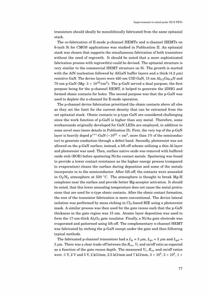
Improvements to metal-polar III-N FETs
transistors should ideally be monolithically fabricated from the same epitaxialstack.
The co-fabrication of E-mode p-channel HEMTs and n-channel HEMTs on6-inch Si for CMOS applications was studied in Publication II. An epitaxialstack was chosen that supports the simultaneous fabrication of both transistorswithout the need of regrowth. It should be noted that a more sophisticatedfabrication process with regrowth(s) could be devised. The epitaxial structure isvery similar to the commercial HEMT structure on Si. The growth is startedwith the AlN nucleation followed by AlGaN buffer layers and a thick (4.2 μm)resistive GaN. The device layers were 420 nm UID GaN, 15 nm Al0.2Ga0.8N and70 nm p-GaN (Mg: 3 × 10¹⁹/cm3). The p-GaN served a dual purpose; the firstpurpose being for the p-channel HEMT, it helped to generate the 2DHG andformed ohmic contacts for holes. The second purpose was that the p-GaN wasused to deplete the n-channel for E-mode operation.
The p-channel device fabrication prioritized the ohmic contacts above all elseas they set the limit for the current density that can be extracted from theset epitaxial stack. Ohmic contacts to p-type GaN are considered challengingsince the work function of p-GaN is higher than any metal. Therefore, someworkarounds originally developed for GaN LEDs are employed, in addition tosome novel ones (more details in Publication II). First, the very top of the p-GaNlayer is heavily doped p+++-GaN (∼1021 × cm3, more than 1% of the semiconduc-tor) to generate conduction through a defect band. Secondly, photoresist was notallowed on the p-GaN surface; instead, a lift-off scheme utilizing a thin Al-layerand photoresist was used. Then, surface native oxide was removed with bufferedoxide etch (BOE) before sputtering Ni/Au contact metals. Sputtering was foundto provide a lower contact resistance as the higher energy process (comparedto evaporation) cleans the surface during deposition and some of the metalsincorporate in to the semiconductor. After lift-off, the contacts were annealedin O2/N2 atmosphere at 550 ◦C. The atmosphere is thought to break Mg-Hcomplexes near the surface and provide better Mg-acceptor activation. It shouldbe noted, that this lower annealing temperature does not cause the metal protru-sions that are used for n-type ohmic contacts. After the ohmic contact formation,the rest of the transistor fabrication is more conventional. The device lateralisolation was performed by mesa etching in Cl2-based RIE using a photoresistmask. A similar process was then used for the gate recess such that the p-GaNthickness in the gate region was 15 nm. Atomic layer deposition was used toform the 17-nm-thick Al2O3 gate insulator. Finally, a Ni/Au gate electrode wasevaporated and patterned using lift-off. The complementary n-channel HEMTwas fabricated by etching the p-GaN except under the gate and then followingtypical methods.
The fabricated p-channel transistors had a Lg = 3 μm, Lgs = 3 μm and Lgd =3 μm. There was a clear trade-off between the Ron, Vt and on/off ratio as expectedas a function of the gate recess depth. The measured Vt, Ron and on/off ratioswere -1 V, 2 V and 5 V, 2 kΩ/mm, 2.5 kΩ/mm and 7 kΩ/mm, 3 × 10⁵, 3 × 10⁵, 1 ×
77
Improvements to metal-polar III-N FETs
105 and 1 × 10³, for p-GaN thicknesses of 9 nm, 15 nm and 21 nm under the gate,respectively. The highest Id was 1.1 mA/mm at Vds = -5 V and Vgs = -11 V. 2DHGdensity and hole drift mobility were 4 × 10¹²/cm2 and 7.5 cm2/V×s respectively.While the hole density in 2DHG is comparable to the electron density in a 2DEG,the mobility is roughly two orders of magnitude lower. Therefore, the channelproperties together with the ohmic contacts explain the challenges experiencedfor the p-channel transistors. Nevertheless, these results are interesting asthey show comparable performance to previous demonstrations, which were onsapphire, on commercially viable 6-inch Si, while simultaneously offering theoption of n-channel HEMTs. Although the p-HEMT performance is currentlylimited, they could prove beneficial in CMOS gate drivers for integrated GaNelectronics in which enhancement-resistor logic is currently used. The channelproperties could be potentially improved by regrowth(s) especially in the gateregion, employing a UID GaN that would improve the hole mobility. N-polarstructures could potentially offer a higher hole mobility when the holes areinduced using polarization.
7.3 Si-ion implanted AlN MESFET
The fabrication of AlN-based Si-ion implanted MESFETs was studied in Publi-cation VII. UWBG AlN holds tremendous potential for high power applicationsdue to a critical electric field four times that of GaN and forty times that of Si[32].
The MESFETs were fabricated from 1-μm-thick AlN templates on sapphiregrown by DOWA Electronics Materials. Si-ion implantations were performed atdifferent angles and energies (see Publication VII for details) to create a uniformdoping profile for the transistor channel and ohmic contacts. The implantationwas simulated to yield a box profile with a depth of 200 nm and concentrationof 1 × 10²⁰/cm3. The Si-donors were thermally activated in a MOVPE reactorat a pyrometer measured surface temperature of 1230 ◦C for 30 min in an N2
atmosphere.Typical fabrication process was used for the AlN MESFETs. After the ion-
implantation, Ti (20 nm)/Al (100 nm)/Ni (25 nm)/Au (50 nm) metal stacks weredeposited using an electron-beam evaporation and patterned using lift-off forsource/drain contacts. The contact metals were annealed at 800 ◦C for 30 s inan N2 ambient. Mesa isolation was obtained by Cl2-based RIE. A Ni (30 nm)/Au(200 nm) metal stack was deposited for the gate electrode.
The electron mobility and sheet carrier concentration of the n-type AlN layerwere 130 cm2/V × s and 6 × 10⁸/cm2, respectively. The carrier concentration ismuch lower than the doping density since the activation ratio in UWBG AlN islow. The MESFETs had a Lg of 2 μm and Lgs of 2 μm. The AlN MESFETs had anormally-on operation and pinch-off voltage (Vgs) of <-10 V. The maximum Id
was 8.7 μA/mm for Vgs = +8 V. The AlN MESFET showed an effective critical
78

Improvements to metal-polar III-N FETs
electric field of 1.0 MV/cm in three terminal Lgd measurements. A three terminalLgd of 2370 V was achieved at Lgd = 25 μm. While these values are better thanthose previously reported for (Al)GaN-buffers, they fall short of the theoreticalEc of 12 MV/cm of AlN. The discrepancy could be due to conduction on the devicesurface or unintentional impurities in the UID AlN buffer.
The AlN MESFET Id was limited by both the channel and contact resistances;nevertheless, it exhibited good breakdown characteristics. The donor-createdchannels are less efficient as semiconductor band gap increases. For UWBGsemiconductor based FETs, polarization induced channels should be employedto increase the channel charge carrier density [32]. Nevertheless, these resultsshow the possibility of fabricating AlN MESFETs and some of these techniquescould be applied to other UWBG devices.
79

8. Prospects of III-N electronics markets
The commercial interest in III-N-based electronics is due to both the demon-strated and potential higher performance over incumbent Si, SiC and GaAstechnologies [14,31,35]. The III-N markets can be split into power electronicsand RF electronics. In power electronics, GaN competes with established Si andSiC-based devices, whereas the competitors in RF electronics are Si and GaAs.The prevalence of Si technology is due to the extreme maturity and economicsof scale which allow to overcome some of the limitations of Si for both powerand RF applications. SiC has been applied to power electronics in which theincreased breakdown field is valuable [31, 32]. On the other hand, GaAs RFelectronics, especially in the form of monolithic microwave integrated circuits(MMICs), are mature and cover some of the RF telecom market, in addition todefense and space applications [14].
The market penetration of especially GaN-based electronics is twofold. First,the GaN devices have enabled applications which have not been previously vi-able, mostly for radio and radar electronics in aerospace and defense applications[13,14]. In these applications, the unit cost has not been a stringent limitationand relatively immature GaN HEMTs have been able to cater for the low volumemarkets. The second wave of GaN adoption, which is currently underway, occursin the more high volume markets of general power electronics and telecom RFelectronics [14,31]. In this case, the increasing maturity of GaN starts to offer ahigher performance per dollar compared to the other semiconductor materials.
The commercial viability of GaN is enhanced by increasing performance figuresof each generation, in addition to adoption of epitaxy on large-area siliconsubstrates and leveraging the development of larger SiC substrates [31, 32].Adoption is further increased as the level of integration increases, in otherwords, the shift from discrete components to integrated circuits. Early playersstart to favor a certain technology when the total system cost breaks even,whereas the actual tipping point for the industry is the component level cost, acase demonstrated by the adoption of SiC and GaAs over Si. However, multipletechnologies are used on the system level as the required level of integrationand other figures of merits change.
81

Prospects of III-N electronics markets
8.1 Power electronics
The power electronics sector is currently split, in terms of voltage and frequency,between the three semiconductors, Si, SiC and GaN, the two former ones beingmost prominent and mature [31,35]. In power electronics, SiC is experiencing asteady adoption over Si. Vertical silicon devices (thyristor, FET and IGBT) havehistorically been able to dominate much of the low frequency (below 100 khz)power applications, whereas lateral MOSFETs have replaced much of the passiveconsumer-market AC-adapters. Vertical technology has expanded the voltagerange of solid-state power electronics into the kVs while being limited to roughlybelow 10 khz. The vertical devices have enabled the electric rail and electricgrid applications for power semiconductors and shown reduced losses in lowervoltage systems such as motor drives, electric vehicles and photovoltaic invertersdue to decreased resistive losses [31,32].
The GaN HEMT is competing on these two fronts. In the case of the lowervoltage switching power, AC-adapters and DC-DC conversion (below 900 V), GaN-on-Si has the potential to replace the incumbent Si technology and overcomethe proposed SiC-based alternatives. This sector encompasses roughly 70% ofthe 15 billion USD total power electronics component/module market [33]. TheGaN power devices currently account for only a 20 million USD market, but arapid growth is expected to roughly 500 million USD by 2023 [33]. This growthis spearheaded by the adoption of the rapid charging applications of consumerelectronics, switching power supplies, electric vehicles as well as by enablingnew applications.
GaN HEMTs offer a much higher operation frequency, which has become atouchstone for power switching, than Si or SiC based transistors. The higherfrequency allows the reduction or elimination of passive components, thussignificantly reducing the overall system footprint [32]. A further reduction insize is due to both the higher power density at reduced resistive losses and up to200 ◦C channel temperature compared to Si maximum junction temperatures,which are closer to 100 ◦C. While GaN-on-Si per unit area is more expensivethan Si, the performance per dollar is offset by the aforementioned factors. Thelow-cost large-area Si substrates for GaN HEMTs allow a reduction of the costbelow that of SiC. However, the the GaN and SiC power devices are on a collisioncourse as the voltage is scaled up.
Medium voltage (1 kV to 2 kV) applications have been ideal for SiC deviceswith competition with GaN being seen at the lower end of this range, whichhas 20% share of the total market [33]. The GaN HEMTs are limited in thisregime as higher breakdown voltages require a larger surface area in the lateraldevices. In contrast, the electric field is easier to handle in vertical SiC devices byincreasing the drift region thickness. Furthermore, SiC MOSFETs can operate atmuch higher temperatures and have better thermal conductivity. GaN HEMTscan be pushed into higher operating voltages by employing SiC substrates. Thisallows higher material quality and thicker layers, which can help to increase
82

Prospects of III-N electronics markets
the breakdown voltage. Simultaneously, the SiC substrate has a higher thermalconductivity and stays more resistive at higher temperatures compared to a Sisubstrate. However, the GaN on SiC significantly increases the cost and bringsthe unit area cost to the level of pure SiC devices. Therefore, the SiC devicesinitially seem to retain the upper hand. In the longer term, the advances in bothtechnologies will decide the outcome in medium voltage applications.
Multiple approaches, some of which are studied in this thesis, have beenproposed to both improve the performance of III-N devices in the current applica-tions and expand the application range. The development of GaN-CMOS wouldincrease the possible level of integration tremendously by enabling monolithicgate driver logic, which is studied in Publication II. Publication I demonstratedincreased isolation of GaN devices when grown on SOI substrates which couldalso enable a higher level of integration.
The voltage handling capability and maximum power density could be signifi-cantly increased by using AlN-based FETs as AlN ideally offers four times thecritical electric field compared to GaN [32]. Thus, the III-N application rangecould be further extended to the medium voltage region and potentially intohigh and very high voltages. The AlN-based FETs are studied in PublicationsIII-IIV. Similarly, GaN as a material is not inherently limited to medium volt-ages, rather the limiting factor is the lack of vertical III-N devices [32]. VerticalIII-N devices are being developed which show significantly higher breakdownvoltages at the expense of operating frequency as they are MOSFETs and notHEMTs [32,178]. The high voltage regime presents untapped applications andgrowth for solid-state power electronics.
8.2 RF electronics
The global RF components market was valued at 18 billion USD in 2018 [28].Similar to the power electronics, the RF electronics is divided between threesemiconductor families. These are Si, traditional III-Vs (GaAs and InP) and GaN.The choice of the material depends on operating frequency, power density andthe level of integration needed for the application. Historically, the solid stateRF electronics were spawned by GaAs MESFET technology in the 1970s whichenabled semiconductors to replace some of the vacuum tube applications [12,13].The real breakthrough was the demonstration of GaAs HEMT and its applicationin the 1990s to commercial telecommunication and military/space radio/radarapplications [15]. Especially the development of MMICs paved the way for anunprecedented level of integration and complexity, which is analogous to thetransition from vacuum tubes to discrete solid state components and eventuallyto integrated circuits [13]. More recently Si, has entered into RF electronics inthe form of laterally diffused metal oxide semiconductor (LDMOS) and SiGebipolar and CMOS technology (BiCMOS). These silicon-based transistors haveseen large-scale use in the cell phone handset front-end modules and base
83

Prospects of III-N electronics markets
stations where they are combined with GaAs hetero-junction bipolar transistor(HBT) RF power amplifiers. GaAs HBTs are preferred over GaAs HEMTs formass markets as the fabrication process can be all-optical lithography. The RFGaAs HEMTs typically require electron beam lithography for the gate module,which significantly increases the cost.
The upcoming 5G networks present a interesting challenge for RF electronicsas operating frequency, power density and the level of integration have tobe increased while lowering the cost. Silicon technology has a high level ofintegration but difficulties in simultaneously achieving high operating frequency(30 GHz to 100 GHz) with suitable power (from 10 W up to 100 W). GaAs offershigher cut-off frequencies and higher power densities than Si. However, GaAshas a higher chip cost than Si due to the substrate price as well as difficulties inreaching very high power densities. It might be possible to gradually improvethese technologies to reach the required performance. However, it is GaNHEMTs that are poised to dominate much of the 5G markets. In addition, asSi and GaAs are expected to be only gradually improved, GaN HEMTs possessmuch untapped potential, and their performance is being improved at a fasterrate [13].
GaN HEMTs and MMICs roughly offer an order of magnitude higher powerdensity in applications below 100 GHz compared to the other semiconductormaterials. In addition, GaN-on-Si RF devices can reduce the substrate costsignificantly impacting chip cost [29, 30]. However, the use of GaN-on-Si forRF applications requires the use of high resistivity substrates which are moreexpensive than standard silicon. Moreover, Si has a lower thermal conductivitythan GaN and becomes more conductive at higher temperatures. The presentfull potential of GaN RF amplifiers can be unleashed on SiC substrates that offera higher crystal quality and three times the thermal conductivity of Si [14,32].The substrate choice ultimately depends on the performance per dollar. As isthe case with GaN LEDs, multiple vendors offer products on both substrates[8]. The RF GaN market is currently valued at 380 million, telecommunicationsoccupying roughly 40%, but it is expected to grow to 1.3 billion USD by 2023,partially due to 5G adoption [179]. In defense applications, the GaN MMICson SiC are steadily replacing their GaAs counterparts. New installations andupgrades are mostly based on GaN due to the much higher attainable powerdensities. The defense applications account for roughly 40% of the GaN RFmarkets [179]. GaAs and InP retain some of the niche applications beyond100 GHz, for example, in radio astronomy [13,14]
In the future, the GaN RF HEMTs could be further improved by using anN-polar structure. The N-polar structures offer many benefits, such as inherentback-barrier for electron confinement, low-resistivity ohmic contacts, and easiervertical scaling [165–169]. These factors can increase the cut-off frequency andpower density significantly [170]. Similarly, AlN-based structures could offer anorder of magnitude higher power density and further scaling of the device dueto increased critical electric field [32,174]. N-polar structures and AlN-based
84

Prospects of III-N electronics markets
FETs were studied in Publications III-IIV.
85


9. Summary
This thesis investigated two areas for improving III-N transistor technology.Namely, methods for a higher level of integration and, on the other hand, ultra-wide band gap (UWBG) AlN-based transistors. For increasing the integration,GaN HEMT epitaxy on 6-inch SOI substrates and the monolithic fabrication of p-and n-channel HEMTs on 6-inch Si substrates were investigated in PublicationsI and II, respectively. Publications III, IV, V and VI present the development ofthe front-end-of-line fabrication process of an N-polar AlN-based PolFET on SiC.Publication VII investigates the fabrication of an ion-implanted AlN MESFET.
The effects of SOI substrate for GaN epitaxy on layer quality and strainwere investigated in Publication I. Synchrotron radiation X-ray topographyanalysis confirmed that the stress relief mechanism in GaN-on-SOI epitaxy isthe formation of a dislocation network to the SOI device Si layer. In addition,the buried oxide layer significantly improves the vertical leakage characteristicsas the onset of the breakdown is delayed by approximately 400 V.
Monolithic fabrication of p- and n-channel HEMTs on 6-inch Si substrates wasinvestigated in Publication II. This study advances the GaN based complemen-tary circuit technology that uses p-GaN gated AlGaN/GaN HEMT by fabricatingp-channel transistor using the same epi-structure as p-GaN-gated n-channeldevices.
Publications III and IV study the nucleation and UID growth of AlN in bothmetal-polar and N-polar configurations. Publication III further confirms theneed to separately optimize the MOVPE growth conditions for metal and N-polar AlN on SiC. The N-polar material requires much higher temperaturesand different V/III-ratio as previously reported in the literature. PublicationIV further expands on the N-polar AlN growth on SiC. The use of N-polar AlNwas previously limited by macro-scale surface roughness due to step-bunchingand micro-hillocks. We showed that by using a reduced substrate miscut, thestep-bunching could be solved. Further, the combination of high growth temper-ature, reduced growth rate and high V/III-ratio was used to control the surfacesupersaturation and eliminate the hexagonal hillocks. Thus, we demonstratedthe first device quality N-polar AlN on SiC.
Publication V discusses the development and optimization of a resistive N-
87

Summary
polar AlN buffer, which was further used to demonstrate an N-polar AlN MES-FET. This is the first demonstration of an N-polar AlN-based transistor. Thebuffer growth was started with a high-temperature nucleation layer for achiev-ing low dislocation density. XRD FWHMs were 120 and 210 arcsec for (002)and (102) reflections, respectively. However, it was discovered that the hightemperature growth leads to unintentional Si incorporation. Therefore, a re-duced temperature layer was grown to act as electrical insulation. The bufferdemonstrated low leakage, 5.6 nA/mm at a 100 V bias. Finally, a Si-doped n++-AlN layer was grown for a MESFET demonstration which exhibited an off-statedrain current of 0.27 nA/mm
The AlN buffer was used as a foundation for an N-polar AlGaN/AlN PoLFETon SiC presented in Publication VI. This is the first demonstration of an N-polarAlN-based polarization doped (PolFET, HEMT) FET. The combination of theN-polar structure, an improved edge-based contact technology and the largecharge density of the polarization-graded 3D electron gas allows the fabricationof devices with more than 120 mA/mm current density. This is the highest valuereported for an AlGaN/AlN heterostructure so far.
Publication VII shows the first demonstration of ion-implanted metal-polarAlN MESFET. The off-state breakdown voltage was 2370 V for drain-to-gatespacing of 25 μm showing the great potential of AlN high-power applications.Ion-implantation can further improve the AlN-based FETs.
The results of this thesis could improve the GaN technology on two fronts. First,the development of GaN-CMOS would increase the possible level of integrationgreatly by enabling monolithic gate driver logic. Secondly, UWBG AlN holdstremendous potential for high power applications due to a critical electric fieldfour times that of GaN and forty times that of Si.
88

References
[1] S. P. Thompson, Dynamo-electric machinery: a manual for students of electrotech-nics. American technical book Company, 1901.
[2] H. Dylla and S. T. Corneliussen, “John Ambrose Fleming and the beginning ofelectronics,” Journal of Vacuum Science & Technology A: Vacuum, Surfaces, andFilms, vol. 23, no. 4, pp. 1244–1251, 2005.
[3] J. Bardeen and W. H. Brattain, “The transistor, a semi-conductor triode,” PhysicalReview, vol. 74, no. 2, p. 230, 1948.
[4] J. S. C. Kilby, “Turning potential into realities: The invention of the integratedcircuit (Nobel lecture),” ChemPhysChem, vol. 2, no. 8-9, pp. 482–489, 2001.
[5] R. Feynman, “There’s plenty of room at the bottom,” in Feynman and computation.CRC Press, 2018, pp. 63–76.
[6] W. Haensch, E. J. Nowak, R. H. Dennard, P. M. Solomon, A. Bryant, O. H.Dokumaci, A. Kumar, X. Wang, J. B. Johnson, and M. V. Fischetti, “Silicon CMOSdevices beyond scaling,” IBM Journal of Research and Development, vol. 50, no.4.5, pp. 339–361, 2006.
[7] E. F. Schubert, T. Gessmann, and J. K. Kim, Light emitting diodes. Wiley OnlineLibrary, 2005.
[8] T.-Y. Seong, J. Han, H. Amano, and H. Morkoc, III-Nitride based light emittingdiodes and applications. Springer Science & Business Media, 2013, vol. 126.
[9] R. Braunstein, “Radiative Transitions in Semiconductors,” Phys. Rev., vol. 99,pp. 1892–1893, Sep 1955. [Online]. Available: https://link.aps.org/doi/10.1103/PhysRev.99.1892
[10] N. Holonyak Jr and S. Bevacqua, “Coherent (visible) light emission fromGaAs1−xPx junctions,” Applied Physics Letters, vol. 1, no. 4, pp. 82–83, 1962.
[11] C. K. Kao, “Nobel Lecture: Sand from centuries past: Send future voices fast,”Reviews of Modern Physics, vol. 82, no. 3, p. 2299, 2010.
[12] R. L. Van Tuyl, C. A. Liechti, R. E. Lee, and E. Gowen, “GaAs MESFET logicwith 4-GHz clock rate,” IEEE Journal of Solid-State Circuits, vol. 12, no. 5, pp.485–496, 1977.
[13] J. A. Del Alamo, “The high-electron mobility transistor at 30: impressive accom-plishments and exciting prospects,” 2011.
[14] R. S. Pengelly, S. M. Wood, J. W. Milligan, S. T. Sheppard, and W. L. Pribble,“A review of GaN on SiC high electron-mobility power transistors and MMICs,”Microwave Theory and Techniques, IEEE Transactions on, vol. 60, no. 6, pp.1764–1783, 2012.
89

References
[15] T. Mimura, S. Hiyamizu, T. Fujii, and K. Nanbu, “A new field-effect transistorwith selectively doped GaAs/n-AlxGa1-xAs heterojunctions,” Japanese Journal ofApplied Physics, vol. 19, no. 5, p. L225, 1980.
[16] M. Niori, T. Saito, K. Joshin, and T. Mimura, “A 20GHz high electron mobilitytransistor amplifier for satellite communications,” in 1983 IEEE InternationalSolid-State Circuits Conference. Digest of Technical Papers, vol. 26. IEEE, 1983,pp. 198–199.
[17] L. Corey, E. Jaska, and J. Guerci, “Phased-array development at DARPA,” inIEEE International Symposium on Phased Array Systems and Technology, 2003.IEEE, 2003, pp. 9–16.
[18] D. Ingram, Y. Chen, J. Kraus, B. Brunner, B. Allen, H. Yen, and K. Lau, “A 427mW, 20% compact W-band InP HEMT MMIC power amplifier,” in 1999 IEEERadio Frequency Integrated Circuits Symposium (Cat No. 99CH37001). IEEE,1999, pp. 95–98.
[19] M. Feng, S.-C. Shen, D. C. Caruth, and J.-J. Huang, “Device technologies for RFfront-end circuits in next-generation wireless communications,” Proceedings ofthe IEEE, vol. 92, no. 2, pp. 354–375, 2004.
[20] H. Amano, I. Akasaki, K. Hiramatsu, N. Koide, and N. Sawaki, “Effects of thebuffer layer in metalorganic vapour phase epitaxy of GaN on sapphire substrate,”Thin Solid Films, vol. 163, pp. 415–420, 1988.
[21] N. Koide, H. Kato, M. Sassa, S. Yamasaki, K. Manabe, M. Hashimoto, H. Amano,K. Hiramatsu, and I. Akasaki, “Doping of GaN with Si and properties of bluem/i/n/n+ 1ga with Si-doped n+-layer by MOVPE,” Journal of Crystal Growth, vol.115, no. 1-4, pp. 639–642, 1991.
[22] S. Nakamura, T. Mukai, and M. Senoh, “Candela-class high-brightness InGaN/Al-GaN double-heterostructure blue-light-emitting diodes,” Applied Physics Letters,vol. 64, no. 13, pp. 1687–1689, 1994.
[23] J. Heber, “Nobel Prize 2014: Akasaki, Amano & Nakamura,” Nature Physics,vol. 10, no. 11, pp. 791–791, 2014.
[24] M. Asif Khan, A. Bhattarai, J. Kuznia, and D. Olson, “High electron mobilitytransistor based on a GaN-Al x Ga1- x N heterojunction,” Applied Physics Letters,vol. 63, no. 9, pp. 1214–1215, 1993.
[25] M. Rosker, C. Bozada, H. Dietrich, A. Hung, D. Via, S. Binari, E. Vivierios,E. Cohen, and J. Hodiak, “The DARPA wide band gap semiconductors for RFapplications (WBGS-RF) program: Phase II results,” CS ManTech, vol. 1, 2009.
[26] M. J. Rosker, J. D. Albrecht, E. Cohen, J. Hodiak, and T.-H. Chang, “DARPA’s GaNtechnology thrust,” in 2010 IEEE MTT-S International Microwave Symposium.IEEE, 2010, pp. 1214–1217.
[27] Z. Popovic, “Amping up the PA for 5G: Efficient GaN power amplifiers withdynamic supplies,” IEEE Microwave Magazine, vol. 18, no. 3, pp. 137–149, 2017.
[28] G. V. Research, “Radio Frequency (RF) Components Market Size,” 2019.
[29] A. Dadgar, “Sixteen years GaN on Si,” Physica Status Solidi (b), vol. 252, no. 5,pp. 1063–1068, 2015.
[30] D. Zhu, D. Wallis, and C. Humphreys, “Prospects of III-nitride optoelectronicsgrown on Si,” Reports on Progress in Physics, vol. 76, no. 10, p. 106501, 2013.
[31] J. Millan, P. Godignon, X. Perpina, A. Perez-Tomas, and J. Rebollo, “A surveyof wide bandgap power semiconductor devices,” IEEE Transactions on PowerElectronics, vol. 29, no. 5, pp. 2155–2163, 2014.
90

References
[32] J. Tsao, S. Chowdhury, M. Hollis, D. Jena, N. Johnson, K. Jones, R. Kaplar,S. Rajan, C. Van de Walle, E. Bellotti et al., “Ultrawide-Bandgap Semiconductors:Research Opportunities and Challenges,” Advanced Electronic Materials, vol. 4,no. 1, p. 1600501, 2018.
[33] M. Rosina, “GaN and SiC power device: market overview,” SEMICON Europa,2018.
[34] H.-C. Chiu, L.-Y. Peng, H.-Y. Wang, H.-C. Wang, H.-L. Kao, G.-Y. Lee, andJ.-I. Chyi, “The Characterization of InAlN/AlN/GaN HEMTs Using Silicon-on-Insulator (SOI) Substrate Technology,” Journal of The Electrochemical Society,vol. 163, no. 2, pp. H110–H114, 2016.
[35] B. Gil, III-nitride semiconductors and their modern devices. Oxford UniversityPress, 2013, vol. 18.
[36] B. J. Baliga, “Gallium nitride devices for power electronic applications,” Semicon-ductor Science and Technology, vol. 28, no. 7, p. 074011, 2013.
[37] H. Morkoç, General properties of nitrides. Wiley Online Library, 2008, vol. 1.
[38] H. Welker, “Über neue halbleitende Verbindungen,” z. Naturforsch. 7a, vol. 744,1952.
[39] W. Johnson and J. Parsons, “Nitrogen compounds of gallium. I, II,” The Journal ofPhysical Chemistry, vol. 36, no. 10, pp. 2588–2594, 1932.
[40] J. Pankove, E. Miller, D. Richman, and J. Berkeyheiser, “Electroluminescence inGaN,” Journal of Luminescence, vol. 4, no. 1, pp. 63–66, 1971.
[41] K. Hiramatsu, S. Itoh, H. Amano, I. Akasaki, N. Kuwano, T. Shiraishi, and K. Oki,“Growth mechanism of GaN grown on sapphire with A1N buffer layer by MOVPE,”Journal of Crystal Growth, vol. 115, no. 1-4, pp. 628–633, 1991.
[42] H. Amano, M. Kito, K. Hiramatsu, and I. Akasaki, “P-type conduction in Mg-doped GaN treated with low-energy electron beam irradiation (LEEBI),” JapaneseJournal of Applied Physics, vol. 28, no. 12A, p. L2112, 1989.
[43] Energy band gap and lattice constant of various semiconductors at roomtemperature. [Online]. Available: http://www.seas.ucla.edu/smrl/GaN.html
[44] M. Mastro, O. Kryliouk, M. Reed, T. Anderson, A. Davydov, and A. Shapiro,“Thermal Stability of MOCVD and HVPE GaN layers in H2, HCl, NH3 and N2,”Physica Status Solidi (a), vol. 188, no. 1, pp. 467–471, 2001.
[45] V. Avrutin, D. J. Silversmith, Y. Mori, F. Kawamura, Y. Kitaoka, and H. Morkoç,“Growth of bulk GaN and AlN: Progress and challenges,” Proceedings of the IEEE,vol. 98, no. 7, pp. 1302–1315, 2010.
[46] D. Holmes, R. Chen, K. Elliott, and C. Kirkpatrick, “Stoichiometry-controlledcompensation in liquid encapsulated Czochralski GaAs,” Applied Physics Letters,vol. 40, no. 1, pp. 46–48, 1982.
[47] K. Sonnenberg and E. Kuessel, “Developments in vertical Bridgman growth oflarge diameter GaAs,” III-Vs Review, vol. 10, no. 5, pp. 30–34, 1997.
[48] K. Hoshino, N. Yanagita, M. Araki, and K. Tadatomo, “Effect of low-temperatureGaN buffer layer on the crystalline quality of subsequent GaN layers grown byMOVPE,” Journal of Crystal Growth, vol. 298, pp. 232–234, 2007.
[49] W. Götz, N. Johnson, J. Walker, D. Bour, and R. Street, “Activation of acceptorsin Mg-doped GaN grown by metalorganic chemical vapor deposition,” AppliedPhysics Letters, vol. 68, no. 5, pp. 667–669, 1996.
91

References
[50] R. Singh, D. Doppalapudi, T. Moustakas, and L. Romano, “Phase separation inInGaN thick films and formation of InGaN/GaN double heterostructures in theentire alloy composition,” Applied Physics Letters, vol. 70, no. 9, pp. 1089–1091,1997.
[51] T. Mukai, M. Yamada, and S. Nakamura, “Characteristics of InGaN-basedUV/blue/green/amber/red light-emitting diodes,” Japanese Journal of AppliedPhysics, vol. 38, no. 7R, p. 3976, 1999.
[52] T. Langer, A. Kruse, F. A. Ketzer, A. Schwiegel, L. Hoffmann, H. Jönen, H. Bre-mers, U. Rossow, and A. Hangleiter, “Origin of the “green gap”: Increasing non-radiative recombination in indium-rich GaInN/GaN quantum well structures,”Physica Status Solidi c, vol. 8, no. 7-8, pp. 2170–2172, 2011.
[53] S. Saito, R. Hashimoto, J. Hwang, and S. Nunoue, “InGaN light-emitting diodes onc-face sapphire substrates in green gap spectral range,” Applied Physics Express,vol. 6, no. 11, p. 111004, 2013.
[54] S. Guha, J. DePuydt, M. Haase, J. Qiu, and H. Cheng, “Degradation of II-VI basedblue-green light emitters,” Applied Physics Letters, vol. 63, no. 23, pp. 3107–3109,1993.
[55] B. J. Baliga, “Power semiconductor device figure of merit for high-frequencyapplications,” IEEE Electron Device Letters, vol. 10, no. 10, pp. 455–457, 1989.
[56] P. H. Woerlee, M. J. Knitel, R. Van Langevelde, D. B. Klaassen, L. F. Tiemeijer,A. J. Scholten, and A. T. Zegers-van Duijnhoven, “RF-CMOS performance trends,”IEEE Transactions on Electron Devices, vol. 48, no. 8, pp. 1776–1782, 2001.
[57] L. D. Nguyen, A. S. Brown, M. A. Thompson, and L. M. Jelloian, “50-nm self-aligned-gate pseudomorphic AlInAs/GaInAs high electron mobility transistors,”IEEE Transactions on Electron Devices, vol. 39, no. 9, pp. 2007–2014, 1992.
[58] F. Lecourt, A. Agboton, N. Ketteniss, H. Behmenburg, N. Defrance, V. Hoel,H. Kalisch, A. Vescan, M. Heuken, and J.-C. De Jaeger, “Power performance at 40GHz on quaternary barrier InAlGaN/GaN HEMT,” IEEE Electron Device Letters,vol. 34, no. 8, pp. 978–980, 2013.
[59] S. Sintonen, “Synchrotron radiation x-ray topography of crystallographic defectsin GaN,” Ph.D. dissertation, Aalto University, 2014.
[60] A. Müller, D. Neculoiu, G. Konstantinidis, A. Stavrinidis, D. Vasilache, A. Cis-maru, M. Danila, M. Dragoman, G. Deligeorgis, and K. Tsagaraki, “6.3-GHz filmbulk acoustic resonator structures based on a gallium nitride/silicon thin rane,”Electron Device Letters, IEEE, vol. 30, no. 8, pp. 799–801, 2009.
[61] A. Konar, A. Verma, T. Fang, P. Zhao, R. Jana, and D. Jena, “Charge transport innon-polar and semi-polar III-V nitride heterostructures,” Semiconductor Scienceand Technology, vol. 27, no. 2, p. 024018, 2012.
[62] Q. Sun, C. D. Yerino, B. Leung, J. Han, and M. E. Coltrin, “Understanding andcontrolling heteroepitaxy with the kinetic Wulff plot: A case study with GaN,”Journal of Applied Physics, vol. 110, no. 5, p. 053517, 2011.
[63] A. Strittmatter, J. E. Northrup, N. M. Johnson, M. V. Kisin, P. Spiberg, H. El-Ghoroury, A. Usikov, and A. Syrkin, “Semi-polar nitride surfaces and heterostruc-tures,” Physica Status Solidi (b), vol. 248, no. 3, pp. 561–573, 2011.
[64] T. Takeuchi, S. Sota, M. Katsuragawa, M. Komori, H. Takeuchi, H. Amano, andI. Akasaki, “Quantum-confined Stark effect due to piezoelectric fields in GaInNstrained quantum wells,” Japanese Journal of Applied Physics, vol. 36, no. 4A, p.L382, 1997.
92

References
[65] S. W. Kaun, M. H. Wong, S. Dasgupta, S. Choi, R. Chung, U. K. Mishra, and J. S.Speck, “Effects of threading dislocation density on the gate leakage of AlGaN/GaNheterostructures for high electron mobility transistors,” Applied Physics Express,vol. 4, no. 2, p. 024101, 2011.
[66] J. Jeschke, A. Knauer, and M. Weyers, “Si impurity concentration in nominallyundoped Al0. 7Ga0. 3N grown in a planetary MOVPE reactor,” Journal of CrystalGrowth, vol. 483, pp. 297–300, 2018.
[67] D. Koleske, A. Wickenden, R. Henry, and M. Twigg, “Influence of MOVPE growthconditions on carbon and silicon concentrations in GaN,” Journal of CrystalGrowth, vol. 242, no. 1-2, pp. 55–69, 2002.
[68] A. Dadgar, P. Veit, F. Schulze, J. Bläsing, A. Krtschil, H. Witte, A. Diez, T. Hempel,J. Christen, R. Clos et al., “MOVPE growth of GaN on Si–Substrates and strain,”Thin Solid Films, vol. 515, no. 10, pp. 4356–4361, 2007.
[69] S. Raghavan, I. C. Manning, X. Weng, and J. M. Redwing, “Dislocation bendingand tensile stress generation in GaN and AlGaN films,” Journal of Crystal Growth,vol. 359, pp. 35–42, 2012.
[70] P. Pampili and P. J. Parbrook, “Doping of III-nitride materials,” Materials Sciencein Semiconductor Processing, vol. 62, pp. 180–191, 2017.
[71] D. D. Koleske, a. E. Wickenden, R. L. Henry, and M. E. Twigg, “Influence ofMOVPE growth conditions on carbon and silicon concentrations in GaN,” Journalof Crystal Growth, vol. 242, pp. 55–69, 2002.
[72] B.-C. Chung and M. Gershenzon, “The influence of oxygen on the electrical andoptical properties of GaN crystals grown by metalorganic vapor phase epitaxy,”Journal of Applied Physics, vol. 72, no. 2, pp. 651–659, 1992.
[73] X. Li, J. Bergsten, D. Nilsson, Ö. Danielsson, H. Pedersen, N. Rorsman, E. Janzén,and U. Forsberg, “Carbon doped GaN buffer layer using propane for high electronmobility transistor applications: Growth and device results,” Applied PhysicsLetters, vol. 107, no. 26, p. 262105, 2015.
[74] S. Heikman, S. Keller, S. P. DenBaars, and U. K. Mishra, “Growth of Fe dopedsemi-insulating GaN by metalorganic chemical vapor deposition,” Applied PhysicsLetters, vol. 81, no. 3, pp. 439–441, 2002.
[75] M. Moram and M. Vickers, “X-ray diffraction of III-nitrides,” Reports on Progressin Physics, vol. 72, no. 3, p. 036502, 2009.
[76] R. Chierchia, T. Böttcher, H. Heinke, S. Einfeldt, S. Figge, and D. Hommel,“Microstructure of heteroepitaxial GaN revealed by x-ray diffraction,” Journal ofApplied Physics, vol. 93, no. 11, pp. 8918–8925, 2003.
[77] H. Amano, M. Kito, K. Hiramatsu, and I. Akasaki, “P-type conduction in Mg-doped GaN treated with low-energy electron beam irradiation (LEEBI),” JapaneseJournal of Applied Physics, vol. 28, no. 12A, p. L2112, 1989.
[78] S. Nakamura, T. Mukai, M. Senoh, and N. Iwasa, “Thermal annealing effects onp-type Mg-doped GaN films,” Japanese Journal of Applied Physics, vol. 31, no. 2B,p. L139, 1992.
[79] L. Yan, Y. Zhang, X. Han, G. Deng, P. Li, Y. Yu, L. Chen, X. Li, and J. Song,“Polarization-induced hole doping in N-polar III-nitride LED grown by metalor-ganic chemical vapor deposition,” Applied Physics Letters, vol. 112, no. 18, p.182104, 2018.
[80] G. B. Stringfellow, Organometallic vapor-phase epitaxy: theory and practice. El-sevier, 1999.
93

References
[81] A. C. Jones and P. O’Brien, CVD of Compound Semiconductors: Precursor Synthe-sis, Developmeny and Applications. John Wiley & Sons, 2008.
[82] B. Łucznik, B. Pastuszka, I. Grzegory, M. Bockowski, G. Kamler, E. Litwin-Staszewska, and S. Porowski, “Deposition of thick GaN layers by HVPE on thepressure grown GaN substrates,” Journal of Crystal Growth, vol. 281, no. 1, pp.38–46, 2005.
[83] B. Heying, R. Averbeck, L. Chen, E. Haus, H. Riechert, and J. Speck, “Controlof GaN surface morphologies using plasma-assisted molecular beam epitaxy,”Journal of Applied Physics, vol. 88, no. 4, pp. 1855–1860, 2000.
[84] R. Dwilinski, R. Doradzinski, J. Garczynski, L. Sierzputowski, A. Puchalski,Y. Kanbara, K. Yagi, H. Minakuchi, and H. Hayashi, “Excellent crystallinity oftruly bulk ammonothermal GaN,” Journal of Crystal Growth, vol. 310, no. 17, pp.3911–3916, 2008.
[85] H. Ishikawa, G.-Y. Zhao, N. Nakada, T. Egawa, T. Jimbo, and M. Umeno, “GaN onSi substrate with AlGaN/AlN intermediate layer,” Japanese Journal of AppliedPhysics, vol. 38, no. 5A, p. L492, 1999.
[86] C. McAleese, M. Kappers, F. Rayment, P. Cherns, and C. Humphreys, “Straineffects of AlN interlayers for MOVPE growth of crack-free AlGaN and AlN/GaNmultilayers on GaN,” Journal of Crystal Growth, vol. 272, no. 1-4, pp. 475–480,2004.
[87] J. Zhang, H. M. Wang, M. E. Gaevski, C. Chen, Q. Fareed, J. Yang, G. Simin,and M. A. Khan, “Crack-free thick AlGaN grown on sapphire using AlN/AlGaNsuperlattices for strain management,” Applied Physics Letters, vol. 80, no. 19, pp.3542–3544, 2002.
[88] J. Sun, J. Chen, X. Wang, J. Wang, W. Liu, J. Zhu, and H. Yang, “Stress reductionin GaN films on (111) silicon-on-insulator substrate grown by metal-organicchemical vapor deposition,” Materials Letters, vol. 61, no. 22, pp. 4416–4419,2007.
[89] J. Cao, D. Pavlidis, Y. Park, J. Singh, and a. Eisenbach, “Improved quality GaN bygrowth on compliant silicon-on-insulator substrates using metalorganic chemicalvapor deposition,” Journal of Applied Physics, vol. 83, no. 7, p. 3829, 1998. [Online].Available: http://scitation.aip.org/content/aip/journal/jap/83/7/10.1063/1.366613
[90] X. Wang, A. Wu, J. Chen, X. Wang, Y. Wu, J. Zhu, and H. Yang, “Study of GaNgrowth on ultra-thin Si membranes,” Solid-State Electronics, vol. 52, no. 6, pp.986–989, 2008.
[91] Q. Jiang, C. Liu, Y. Lu, and K. J. Chen, “1.4-kV AlGaN/GaN HEMTs on a GaN-on-SOI platform,” IEEE Electron Device Letters, vol. 34, no. 3, pp. 357–359, 2013.
[92] X. Wang, A. Wu, J. Chen, X. Wang, Y. Wu, J. Zhu, and H. Yang, “Study of GaNgrowth on ultra-thin Si membranes,” Solid-State Electronics, vol. 52, no. 6, pp.986–989, 2008.
[93] X. Li, M. Van Hove, M. Zhao, K. Geens, V.-P. Lempinen, J. Sormunen, G. Groe-seneken, and S. Decoutere, “200 V enhancement-mode p-GaN HEMTs fabricatedon 200 mm GaN-on-SOI with trench isolation for monolithic integration,” IEEEElectron Device Letters, vol. 38, no. 7, pp. 918–921, 2017.
[94] T. J. Anderson, A. D. Koehler, M. J. Tadjer, J. K. Hite, A. Nath, N. A. Mahadik,O. Aktas, V. Odnoblyudov, C. Basceri, K. D. Hobart et al., “Electrothermal eval-uation of thick GaN epitaxial layers and AlGaN/GaN high-electron-mobilitytransistors on large-area engineered substrates,” Applied Physics Express, vol. 10,no. 12, p. 126501, 2017.
94

References
[95] H. Brune, Epitaxial Growth of Thin Films. Wiley-VCH Verlag GmbH &Co. KGaA, 2013, pp. 421–492. [Online]. Available: http://dx.doi.org/10.1002/9783527680566.ch20
[96] Schematische Darstellung einer MOCVD Apparatur. [Online]. Avail-able: https://www.ifkp.tu-berlin.de/menue/arbeitsgruppen/ag_bimberg/forschung/labore_und_experimentelle_techniken/epitaxie/
[97] M. Bosi and R. Fornari, “A study of Indium incorporation efficiency in InGaNgrown by MOVPE,” Journal of Crystal Growth, vol. 265, no. 3-4, pp. 434–439,2004.
[98] M. Imura, H. Sugimura, N. Okada, M. Iwaya, S. Kamiyama, H. Amano, I. Akasaki,and A. Bandoh, “Impact of high-temperature growth by metal-organic vaporphase epitaxy on microstructure of AlN on 6H-SiC substrates,” Journal of CrystalGrowth, vol. 310, no. 7-9, pp. 2308–2313, 2008.
[99] S. Mita, R. Collazo, A. Rice, R. Dalmau, and Z. Sitar, “Influence of galliumsupersaturation on the properties of GaN grown by metalorganic chemical vapordeposition,” Journal of Applied Physics, vol. 104, no. 1, p. 013521, 2008.
[100] S. Mita, R. Collazo, A. Rice, J. Tweedie, J. Xie, R. Dalmau, and Z. Sitar, “Impactof gallium supersaturation on the growth of N-polar GaN,” Physica Status Solidi(C) Current Topics in Solid State Physics, vol. 8, no. 7-8, pp. 2078–2080, 2011.
[101] T. Webb, CCS6x2FT System Manual, 3rd ed., Aixtron, September 2013.
[102] R. P. Parikh and R. A. Adomaitis, “An overview of gallium nitride growth chem-istry and its effect on reactor design: Application to a planetary radial-flow CVDsystem,” Journal of Crystal Growth, vol. 286, no. 2, pp. 259–278, 2006.
[103] Acarlso3. Growth modes of thin films. [Online]. Available: https://en.wikipedia.org/wiki/Stranski%E2%80%93Krastanov_growth
[104] X. Sun, D. Li, Y. Chen, H. Song, H. Jiang, Z. Li, G. Miao, and Z. Zhang, “Insitu observation of two-step growth of AlN on sapphire using high-temperaturemetal–organic chemical vapour deposition,” CrystEngComm, vol. 15, no. 30, pp.6066–6073, 2013.
[105] S. Kim, J. Oh, J. Kang, D. Kim, J. Won, J. W. Kim, and H. K. Cho, “Two-stepgrowth of high quality GaN using V/III ratio variation in the initial growth stage,”Journal of Crystal Growth, vol. 262, no. 1-4, pp. 7–13, 2004.
[106] I. Bryan, Z. Bryan, S. Mita, A. Rice, J. Tweedie, R. Collazo, and Z. Sitar, “Surfacekinetics in AlN growth: A universal model for the control of surface morphologyin III-nitrides,” Journal of Crystal Growth, vol. 438, pp. 81–89, 2016.
[107] K. Bellmann, U. W. Pohl, C. Kuhn, T. Wernicke, and M. Kneissl, “Controllingthe morphology transition between step-flow growth and step-bunching growth,”Journal of Crystal Growth, vol. 478, pp. 187–192, 2017.
[108] S. Keller, H. Li, M. Laurent, Y. Hu, N. Pfaff, J. Lu, D. F. Brown, N. A. Fichtenbaum,J. S. Speck, S. P. Denbaars, and U. K. Mishra, “Recent progress in metal-organicchemical vapor deposition of (000-1) N-polar group-III nitrides,” SemiconductorScience and Technology, vol. 29, p. 113001, 2014.
[109] M. H. Wong, S. Keller, N. Dasgupta, D. J. Denninghoff, S. Kolluri, D. F.Brown, J. Lu, N. a. Fichtenbaum, E. Ahmadi, U. Singisetti, A. Chini,S. Rajan, S. P. DenBaars, J. S. Speck, and U. K. Mishra, “N-polarGaN epitaxy and high electron mobility transistors,” Semiconductor Scienceand Technology, vol. 28, no. 7, p. 74009, 2013. [Online]. Available:http://iopscience.iop.org/0268-1242/28/7/074009/article/
95

References
[110] T. K. Zywietz, J. Neugebauer, and M. Scheffler, “The adsorption of oxygen atGaN surfaces,” Applied Physics Letters, vol. 74, no. 12, p. 1695, 1999. [Online].Available: http://scitation.aip.org/content/aip/journal/apl/74/12/10.1063/1.123658
[111] T. Zywietz, J. Neugebauer, and M. Scheffler, “Adatom diffusion at GaN (0001) and(000-1) surfaces,” Applied Physics Letters, vol. 73, no. 4, pp. 487–489, 1998.
[112] A. R. A. Zauner, E. Aret, W. J. P. Van Enckevort, J. L. Weyher, S. Porowski, andJ. J. Schermer, “Homo-epitaxial growth on the N-face of GaN single crystals: Theinfluence of the misorientation on the surface morphology,” Journal of CrystalGrowth, vol. 240, no. 1-2, pp. 14–21, 2002.
[113] J. Weyher, P. Brown, A. Zauner, S. Müller, C. Boothroyd, D. Foord, P. Hageman,C. Humphreys, P. Larsen, I. Grzegory, and S. Porowski, “Morphological andstructural characteristics of homoepitaxial GaN grown by metalorganic chemicalvapour deposition (MOCVD),” Journal of Crystal Growth, vol. 204, no. 4, pp.419–428, 1999.
[114] T. Matsuoka, Y. Kobayashi, H. Takahata, T. Mitate, S. Mizuno, A. Sasaki, M. Yoshi-moto, T. Ohnishi, and M. Sumiya, “N-polarity GaN on sapphire substrate grown byMOVPE,” Physica Status Solidi (B) Basic Research, vol. 243, no. 7, pp. 1446–1450,2006.
[115] S. Keller, C. S. Suh, Z. Chen, R. Chu, S. Rajan, N. A. Fichtenbaum, M. Furukawa,S. P. DenBaars, J. S. Speck, and U. K. Mishra, “Properties of N-polar AlGaN/GaNheterostructures and field effect transistors grown by metalorganic chemicalvapor deposition,” Journal of Applied Physics, vol. 103, no. 3, pp. 1–5, 2008.
[116] S. Keller, N. A. Fichtenbaum, F. Wu, D. Brown, A. Rosales, S. P. Denbaars,J. S. Speck, and U. K. Mishra, “Influence of the substrate misorientation onthe properties of N-polar GaN films grown by metal organic chemical vapordeposition,” Journal of Applied Physics, vol. 102, no. 8, 2007.
[117] S. Keller, N. Fichtenbaum, F. Wu, G. Lee, S. P. Denbaars, J. S. Speck, and U. K.Mishra, “Effect of the nucleation conditions on the polarity of AlN and GaN filmsgrown on C-face 6H-SiC,” Japanese Journal of Applied Physics, Part 2: Letters,vol. 45, no. 8-11, 2006.
[118] D. Won and J. M. Redwing, “Effect of AlN buffer layers on the surface morphologyand structural properties of N-polar GaN films grown on vicinal C-face SiCsubstrates,” Journal of Crystal Growth, vol. 377, pp. 51–58, 2013. [Online].Available: http://dx.doi.org/10.1016/j.jcrysgro.2013.04.038
[119] D. Won, X. Weng, Z. Y. Al Balushi, and J. M. Redwing, “Influence of growth stresson the surface morphology of N-polar GaN films grown on vicinal C-face SiCsubstrates,” Applied Physics Letters, vol. 103, no. 24, 2013.
[120] M. Sakai, H. Ishikawa, T. Egawa, T. Jimbo, M. Umeno, T. Shibata, K. Asai,S. Sumiya, Y. Kuraoka, M. Tanaka, and O. Oda, “Growth of high-quality GaNfilms on epitaxial AlN/sapphire templates by MOVPE,” Journal of Crystal Growth,vol. 244, no. 1, pp. 6–11, 2002.
[121] H. Lahrèche, P. Vennéguès, O. Tottereau, M. Laügt, P. Lorenzini, M. Leroux,B. Beaumont, and P. Gibart, “Optimisation of AlN and GaN growth by metalor-ganic vapour-phase epitaxy (MOVPE) on Si(111),” Journal of Crystal Growth, vol.217, no. 1, pp. 13–25, 2000.
[122] M. Imura, H. Sugimura, N. Okada, M. Iwaya, S. Kamiyama, H. Amano, I. Akasaki,and A. Bandoh, “Impact of high-temperature growth by metal-organic vaporphase epitaxy on microstructure of AlN on 6H-SiC substrates,” Journal of CrystalGrowth, vol. 310, no. 7-9, pp. 2308–2313, 2008.
96

References
[123] H. J. Kim, S. Choi, D. Yoo, J. H. Ryou, R. D. Dupuis, R. F. Dalmau, P. Lu, andZ. Sitar, “Modulated precursor flow epitaxial growth of AlN layers on native AlNsubstrates by metal-organic chemical vapor deposition,” Applied Physics Letters,vol. 93, no. 2, pp. 2006–2009, 2008.
[124] S. Keller, Y. Dora, F. Wu, X. Chen, S. Chowdury, S. P. Denbaars, J. S. Speck, andU. K. Mishra, “Properties of N-polar GaN films and AlGaN/GaN heterostructuresgrown on (111) silicon by metal organic chemical vapor deposition,” AppliedPhysics Letters, vol. 97, no. 14, pp. 1–4, 2010.
[125] R. G. Banal, M. Funato, and Y. Kawakami, “Surface diffusion during metalorganicvapor phase epitaxy of AlN,” Physica Status Solidi C, vol. 6, no. 2, pp. 599 – 602,2009.
[126] D. Won and J. M. Redwing, “Effect of AlN buffer layers on the surface morphologyand structural properties of N-polar GaN films grown on vicinal C-face SiCsubstrates,” Journal of Crystal Growth, vol. 377, pp. 51–58, 2013. [Online].Available: http://dx.doi.org/10.1016/j.jcrysgro.2013.04.038
[127] T. Sasaki and T. Matsuoka, “Substrate-polarity dependence of metal-organicvapor-phase epitaxy-grown GaN on SiC,” Journal of Applied Physics, vol. 64, no. 9,pp. 4531–4535, 1988.
[128] M. Kurimoto, M. Shibata, J. Yamamoto, M. Tsubamoto, T. Honda, and H. Kawan-ishi, “Direct growth of GaN on (0 0 0 1) 6H–SiC by low-pressure MOVPE with aflow channel,” Journal of Crystal Growth, vol. 189, pp. 189–192, 1998.
[129] D. F. Brown, S. Keller, F. Wu, J. S. Speck, S. P. DenBaars, and U. K. Mishra,“Growth and characterization of N-polar GaN films on SiC by metal organicchemical vapor deposition,” Journal of Applied Physics, vol. 104, no. 2, pp. 1–6,2008.
[130] S. Kolluri, S. Member, S. Keller, S. P. Denbaars, and U. K. Mishra, “MicrowavePower Performance N-Polar GaN MISHEMTs Grown by MOCVD on SiC Sub-strates Using an Al2O3 Etch-Stop Technology,” IEEE Electron Device Letters,vol. 33, no. 1, pp. 44–46, 2012.
[131] D. F. Brown, R. Chu, S. Keller, S. P. Denbaars, and U. K. Mishra, “Electricalproperties of N-polar AlGaN/GaN high electron mobility transistors grown onSiC by metalorganic chemical vapor deposition,” Applied Physics Letters, vol. 94,no. 15, pp. 148–151, 2009.
[132] D. K. Schroder, Semiconductor material and device characterization. John Wiley& Sons, 2006.
[133] EpiCurve TT for AIXTRON Close Couple Showerhead MOCVD systems, 1st ed.,Laytec, August 2009.
[134] D. Zhu, C. McAleese, K. McLaughlin, M. Häberlen, C. Salcianu, E. Thrush,M. Kappers, W. Phillips, P. Lane, D. Wallis et al., “GaN-based LEDs grown on6-inch diameter Si (111) substrates by MOVPE,” in SPIE OPTO: IntegratedOptoelectronic Devices. International Society for Optics and Photonics, 2009, pp.723 118–723 118.
[135] F. Brunner, A. Knauer, T. Schenk, M. Weyers, and J.-T. Zettler, “Quantitativeanalysis of in situ wafer bowing measurements for III-nitride growth on sapphire,”Journal of Crystal Growth, vol. 310, no. 10, pp. 2432–2438, 2008.
[136] A. MarcoTolo, Steff, “File:Schema MEB (en).svg,” https ://commons.wikimedia.org/wiki/File : SchemaMEB(en).svg.
97

References
[137] G. Kamler, J. L. Weyher, I. Grzegory, E. Jezierska, and T. Wosinski, “Defect-selective etching of GaN in a modified molten bases system,” Journal of CrystalGrowth, vol. 246, no. 1-2, pp. 21–24, 2002.
[138] J. L. Weyher, P. D. Brown, J. L. Rouvière, T. Wosinski, A. R. A. Zauner, andI. Grzegory, “Recent advances in defect-selective etching of GaN,” Journal ofCrystal Growth, vol. 210, no. 1, pp. 151–156, 2000.
[139] J. L. Rouviere, J. L. Weyher, M. Seelmann-Eggebert, and S. Porowski, “Polaritydetermination for GaN films grown on (0001) sapphire and high-pressure-grownGaN single crystals,” Applied Physics Letters, vol. 73, no. 5, pp. 668–670, 1998.
[140] Y. Fu, Q. Fan, S. Chevtchenko, Ü. Özgür, H. Morkoç, Y. Ke, R. Devaty,W. J. Choyke, C. K. Inoki, and T. S. Kuan, “Growth and polarity controlof GaN and AlN on carbon-face SiC by metalorganic vapor phase epitaxy,”Proceedings of SPIE, vol. 6473, p. 647305, 2007. [Online]. Available: http://proceedings.spiedigitallibrary.org/proceeding.aspx?doi=10.1117/12.706938
[141] B. D. Cullity and S. R. Stock, Elements of X-ray Diffraction. Pearson, 2001.
[142] J. Weyher, S. Lazar, L. Macht, Z. Liliental-Weber, R. Molnar, S. Müller, V. Sivel,G. Nowak, and I. Grzegory, “Orthodox etching of HVPE-grown GaN,” Journal ofCrystal Growth, vol. 305, no. 2, pp. 384–392, 2007.
[143] A. Lankinen, T. O. Tuomi, P. Kostamo, H. Jussila, S. Sintonen, H. Lipsanen,M. Tilli, J. Mäkinen, and A. N. Danilewsky, “Synchrotron X-ray diffractiontopography study of bonding-induced strain in silicon-on-insulator wafers,”Thin Solid Films, vol. 603, pp. 435–440, 2016. [Online]. Available:http://www.sciencedirect.com/science/article/pii/S0040609016001516
[144] T. Tuomi, K. Naukkarinen, and P. Rabe, “Use of synchrotron radiation in X-raydiffraction topography,” Physica Status Solidi (a), vol. 25, no. 1, pp. 93–106, 1974.
[145] T. Tuomi, “Synchrotron X-ray topography of electronic materials,” Journal ofSynchrotron Radiation, vol. 9, no. 3, pp. 174–178, 2002.
[146] P. McNally, J. Curley, M. Bolt, A. Reader, T. Tuomi, R. Rantama, A. Danilewsky,I. Dewolf et al., “Monitoring of stress reduction in shallow trench isolation CMOSstructures via synchrotron X-ray topography, electrical data and raman spec-troscopy,” Journal of Materials Science: Materials in Electronics, vol. 10, no. 5-6,pp. 351–358, 1999.
[147] A. Rack, T. Weitkamp, S. Bauer Trabelsi, P. Modregger, A. Cecilia,T. dos Santos Rolo, T. Rack, D. Haas, R. Simon, R. Heldele, M. Schulz,B. Mayzel, A. N. Danilewsky, T. Waterstradt, W. Diete, H. Riesemeier, B. R.M??ller, and T. Baumbach, “The micro-imaging station of the TopoTomobeamline at the ANKA synchrotron light source,” Nuclear Instruments andMethods in Physics Research, Section B: Beam Interactions with Materialsand Atoms, vol. 267, no. 11, pp. 1978–1988, 2009. [Online]. Available:http://dx.doi.org/10.1016/j.nimb.2009.04.002
[148] S. Binari, L. Rowland, W. Kruppa, G. Kelner, K. Doverspike, and D. Gaskill,“Microwave performance of GaN MESFETS,” Electronics letters, vol. 30, no. 15,pp. 1248–1249, 1994.
[149] G. Greco, F. Iucolano, and F. Roccaforte, “Review of technology for normally-offHEMTs with p-GaN gate,” Materials Science in Semiconductor Processing, vol. 78,pp. 96–106, 2018.
[150] O. Hilt, A. Knauer, F. Brunner, E. Bahat-Treidel, and J. Würfl, “Normally-offAlGaN/GaN HFET with p-type Ga Gate and AlGaN buffer,” in 2010 22nd Inter-national Symposium on Power Semiconductor Devices & IC’s (ISPSD). IEEE,2010, pp. 347–350.
98

References
[151] T. Mizutani, M. Ito, S. Kishimoto, and F. Nakamura, “AlGaN/GaN HEMTs withthin InGaN cap layer for normally off operation,” IEEE Electron Device Letters,vol. 28, no. 7, pp. 549–551, 2007.
[152] X. Li, M. Van Hove, M. Zhao, K. Geens, W. Guo, S. You, S. Stoffels, V.-P. Lempinen,J. Sormunen, G. Groeseneken et al., “Suppression of the backgating effect ofenhancement-mode p-GaN HEMTs on 200-mm GaN-on-SOI for monolithic inte-gration,” IEEE Electron Device Letters, vol. 39, no. 7, pp. 999–1002, 2018.
[153] E. Moore, Y. Yeo, M.-Y. Ryu, and R. Hengehold, “Nearly Perfect Electrical Acti-vation Efficiencies from Silicon-Implanted Al x Ga 1- x N with High AluminumMole Fraction,” Journal of Electronic Materials, vol. 38, no. 1, pp. 153–158, 2009.
[154] J. P. de Souza and D. K. Sadana, “Ion implantation in gallium arsenide MESFETtechnology,” IEEE Transactions on Electron Devices, vol. 39, no. 1, pp. 166–175,1992.
[155] A. Teke, S. Gökden, R. Tülek, J. Leach, Q. Fan, J. Xie, Ü. Özgür, H. Morkoç,S. Lisesivdin, and E. Özbay, “The effect of AlN interlayer thicknesses on scat-tering processes in lattice-matched AlInN/GaN two-dimensional electron gasheterostructures,” New Journal of Physics, vol. 11, no. 6, p. 063031, 2009.
[156] J. Zhang, S. Huang, Q. Bao, X. Wang, K. Wei, Y. Zheng, Y. Li, C. Zhao, X. Liu,Q. Zhou et al., “Mechanism of Ti/Al/Ti/W Au-free ohmic contacts to AlGaN/GaNheterostructures via pre-ohmic recess etching and low temperature annealing,”Applied Physics Letters, vol. 107, no. 26, p. 262109, 2015.
[157] S. Ruvimov, Z. Liliental-Weber, J. Washburn, K. Duxstad, E. Haller, Z.-F. Fan,S. N. Mohammad, W. Kim, A. Botchkarev, and H. Morkoc, “Microstructure ofTi/Al and Ti/Al/Ni/Au Ohmic contacts for n-GaN,” Applied Physics Letters, vol. 69,no. 11, pp. 1556–1558, 1996.
[158] Z. Fan, S. N. Mohammad, W. Kim, Ö. Aktas, A. E. Botchkarev, and H. Morkoç,“Very low resistance multilayer Ohmic contact to n-GaN,” Applied Physics Letters,vol. 68, no. 12, pp. 1672–1674, 1996.
[159] B. De Jaeger, M. Van Hove, D. Wellekens, X. Kang, H. Liang, G. Mannaert,K. Geens, and S. Decoutere, “Au-free CMOS-compatible AlGaN/GaN HEMTprocessing on 200 mm Si substrates,” in 2012 24th International Symposium onPower Semiconductor Devices and ICs. IEEE, 2012, pp. 49–52.
[160] J. P. Ibbetson, P. Fini, K. Ness, S. DenBaars, J. Speck, and U. Mishra, “Polarizationeffects, surface states, and the source of electrons in AlGaN/GaN heterostructurefield effect transistors,” Applied Physics Letters, vol. 77, no. 2, pp. 250–252, 2000.
[161] H. Xiao-Guang, Z. De-Gang, and J. De-Sheng, “Formation of two-dimensionalelectron gas at AlGaN/GaN heterostructure and the derivation of its sheet densityexpression,” Chinese Physics B, vol. 24, no. 6, p. 067301, 2015.
[162] I. Smorchkova, C. Elsass, J. Ibbetson, R. Vetury, B. Heying, P. Fini, E. Haus,S. DenBaars, J. Speck, and U. Mishra, “Polarization-induced charge and electronmobility in AlGaN/GaN heterostructures grown by plasma-assisted molecular-beam epitaxy,” Journal of Applied Physics, vol. 86, no. 8, pp. 4520–4526, 1999.
[163] M. Grundmann, “BandEng, 1D Schrodinger-Poisson Solver Software.”
[164] S. Bajaj, T.-H. Hung, F. Akyol, D. Nath, and S. Rajan, “Modeling of high com-position AlGaN channel high electron mobility transistors with large thresholdvoltage,” Applied Physics Letters, vol. 105, no. 26, p. 263503, 2014.
[165] S. Rajan, A. Chini, M. H. Wong, J. S. Speck, and U. K. Mishra, “N-polar GaNAl-GaNGaN high electron mobility transistors,” Journal of Applied Physics, vol. 102,no. 4, 2007.
99

References
[166] S. Dasgupta, Nidhi, D. F. Brown, F. Wu, S. Keller, J. S. Speck, and U. K. Mishra,“Ultralow nonalloyed Ohmic contact resistance to self aligned N-polar GaN highelectron mobility transistors by In(Ga)N regrowth,” Applied Physics Letters,vol. 96, no. 14, 2010.
[167] M. H. Wong, Y. Pei, T. Palacios, L. Shen, A. Chakraborty, L. S. McCarthy, S. Keller,S. P. Denbaars, J. S. Speck, and U. K. Mishra, “Low nonalloyed Ohmic contactresistance to nitride high electron mobility transistors using N-face growth,”Applied Physics Letters, vol. 91, no. 23, pp. 1–4, 2007.
[168] P. S. Park, D. N. Nath, and S. Rajan, “Quantum capacitance in N-polar GaN/Al-GaN/GaN heterostructures,” IEEE Electron Device Letters, vol. 33, no. 7, pp.991–993, 2012.
[169] J. Kuzmík, “N-polarity InN/GaN/InAlN high-electron-mobility transistors,” Ap-plied Physics Express, vol. 5, no. 4, 2012.
[170] U. Singisetti, M. H. Wong, and U. K. Mishra, “High-performance N-polar GaNenhancement-mode device technology,” Semiconductor Science and Technology,vol. 28, no. 7, p. 074006, 2013.
[171] A. G. Baca, A. M. Armstrong, A. A. Allerman, E. A. Douglas, C. A. Sanchez, M. P.King, M. E. Coltrin, T. R. Fortune, and R. J. Kaplar, “An AlN/Al0. 85Ga0. 15N highelectron mobility transistor,” Applied Physics Letters, vol. 109, no. 3, p. 033509,2016.
[172] S. Rajan, H. Xing, S. DenBaars, U. K. Mishra, and D. Jena, “AlGaN/GaNpolarization-doped field-effect transistor for microwave power applications,” Ap-plied Physics Letters, vol. 84, no. 9, pp. 1591–1593, 2004.
[173] Y. Fang, Z. Feng, J. Yin, X. Zhou, Y. Wang, G. Gu, X. Song, Y. Lv, C. Li, and S. Cai,“AlGaN/GaN polarization-doped field-effect transistors with graded heterostruc-ture,” IEEE Transactions on Electron Devices, vol. 61, no. 12, pp. 4084–4089,2014.
[174] A. G. Baca, B. A. Klein, J. R. Wendt, S. M. Lepkowski, C. D. Nordquist, A. M.Armstrong, A. A. Allerman, E. A. Douglas, and R. J. Kaplar, “RF Performance ofAl 0.85 Ga 0.15 N/Al 0.70 Ga 0.30 N High Electron Mobility Transistors With80-nm Gates,” IEEE Electron Device Letters, vol. 40, no. 1, pp. 17–20, 2018.
[175] T. Fang, R. Wang, H. Xing, S. Rajan, and D. Jena, “Effect of optical phononscattering on the performance of GaN transistors,” IEEE Electron Device Letters,vol. 33, no. 5, pp. 709–711, 2012.
[176] R. Gaska, Q. Chen, J. Yang, A. Osinsky, M. A. Khan, and M. S. Shur, “High-temperature performance of AlGaN/GaN HFETs on SiC substrates,” IEEE Elec-tron Device Letters, vol. 18, no. 10, pp. 492–494, 1997.
[177] C. Liu, E. F. Chor, and L. S. Tan, “Enhanced device performance of AlGaN/GaNHEMTs using HfO2 high-k dielectric for surface passivation and gate oxide,”Semiconductor Science and Technology, vol. 22, no. 5, p. 522, 2007.
[178] T. Oka, T. Ina, Y. Ueno, and J. Nishii, “1.8 mΩ· cm2 vertical GaN-based trenchmetal–oxide–semiconductor field-effect transistors on a free-standing GaN sub-strate for 1.2-kV-class operation,” Applied Physics Express, vol. 8, no. 5, p. 054101,2015.
[179] “RF GaN Market: Applications, Players, Technology, and Substrates 2018-2023,”Yole Développement, 2018.
100

-otl
aA
DD
76
1/
02
02
+fejaa
e*GMFTSH
9
NBSI 5-4900-46-259-879 )detnirp(
NBSI 2-5900-46-259-879 )fdp(
NSSI 4394-9971 )detnirp(
NSSI 2494-9971 )fdp(
ytisrevinU otlaA
gnireenignE lacirtcelE fo loohcS
gnireenigneonaN dna scinortcelE fo tnemtrapeD
fi.otlaa.www
+ SSENISUB YMONOCE
+ TRA
+ NGISED ERUTCETIHCRA
+ ECNEICS
YGOLONHCET
REVOSSORC
LAROTCOD SNOITATRESSID
ne
nitt
em
eL
iroJ
yg
olo
nhc
et r
otsi
sna
rt t
cef
fe-
dle
fi N-
III
laix
ati
pe
ot s
tn
em
evor
pmI
yti
srev
in
U otl
aA
0202
gnireenigneonaN dna scinortcelE fo tnemtrapeD
laixatipe ot stnemevorpmI rotsisnart tceffe-dlefi N-III
ygolonhcet
nenittemeL iroJ
LAROTCOD SNOITATRESSID