Embed Size (px)
Citation preview

KATIHAL FİZİĞİ MNT-510
YARIİLETKENLER
Kaynaklar: Katıhal Fiziği, Prof. Dr. Mustafa Dikici, Seçkin Yayıncılık Katıhal Fiziği, Şakir Aydoğan, Nobel Yayıncılık, Physics for Computer Science Students: With Emphasis on Atomic and Semiconductor Physics, Narciso Garcia, Arthur Damask, Steven Schwarz, Springer Lecture Notes, Prof. A. Niknejad, University of California, Berkley

• The highest energy band completely filled with electrons (at T = 0 K) is called the Valence Band
• The next band is called the Conduction Band
• The energy difference between the bottom of the Conduction and the top of the Valence bands is called the Band Gap

Conduction
• Electron Conduction is easy to imagine: electrons (in the conduction band) move almost like free particles
• Hole Conduction is due to positively charged particles in the valence band

Intrinsic Semiconductors • Consider nominally pure
semiconductor at T = 0 K • There is no electrons in the
conduction band
• At T > 0 K a small fraction of electrons is thermally excited into the conduction band, “leaving” the same number of holes in the valence band

Intrinsic Semiconductors at T >0 K
• Electrons and holes contribute to the current when a voltage is applied

Carrier Concentrations at T >0 K • Let’s take EV = 0, then EC = EG
• The number of electrons equals the number of holes, ne = nh • The Fermi level lies in the middle of the band gap
• ne = nh increase rapidly with temperature

Carrier Concentrations • EG of selected semiconductors ▫ Si: 1.1eV ▫ Ge: 0.7eV ▫ GaAs: 1.4eV ▫ ZnSe: 2.7eV
• Carrier effective masses for selected semiconductors ▫ GaAs: me
*= 0.067m0; mh*= 0.45m0
▫ Si: me* = 0.26m0; mh
* = 0.49m0
▫ Ge: me* = 0.04m0; mh
* = 0.28m0
▫ ZnSe: me* = 0.21m0; mh
* = 0.74m0
Carrier concentration falls with 1/T, i.e. increase with T

Doping
• Semiconductors can be easily doped • Doping is the incorporation of [substitutional] impurities into a
semiconductor according to our requirements
• In other words, impurities are introduced in a controlled manner Impurities change the conductivity of the material so that it can be
fabricated into a device

Extrinsic Semiconductors • Electrical Properties of Semiconductors can be altered
drastically by adding minute amounts of suitable impurities to the pure crystals
• Impurities: Atoms of the elements different from those forming solid ▫ Interstitial: “foreign” atoms “squeezed” between regular
sites crystal sites ▫ Substitutional: “foreign” atoms occupying the sites of
host atoms

Donors • We use Silicon (Si) as an example ▫ Substitute one Si (Group IV) atom with a Group V atom
(e.g. As or P) ▫ Si atoms have four valence electrons that participate in
covalent bonding ▫ When a Group V atom replaces a Si atom, it will use
four of its electrons to form the covalent bonding ▫ What happens with the remaining electron?
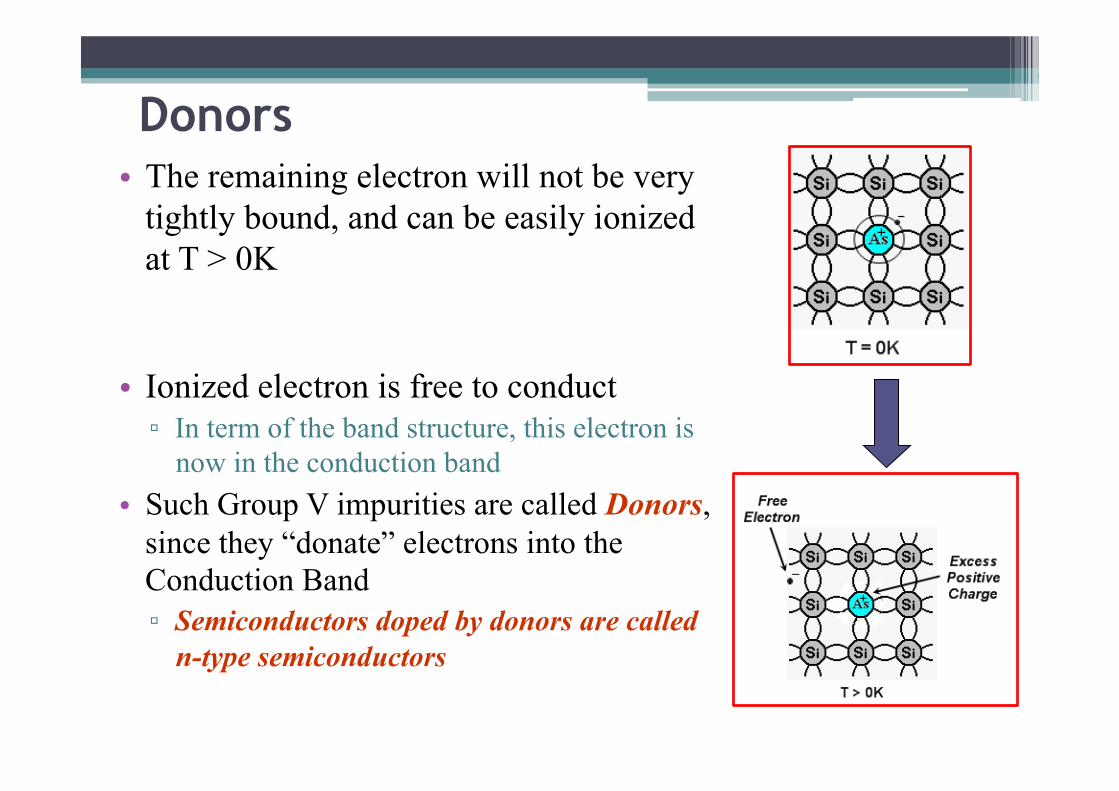
Donors • The remaining electron will not be very
tightly bound, and can be easily ionized at T > 0K
• Ionized electron is free to conduct ▫ In term of the band structure, this electron is
now in the conduction band • Such Group V impurities are called Donors,
since they “donate” electrons into the Conduction Band ▫ Semiconductors doped by donors are called
n-type semiconductors

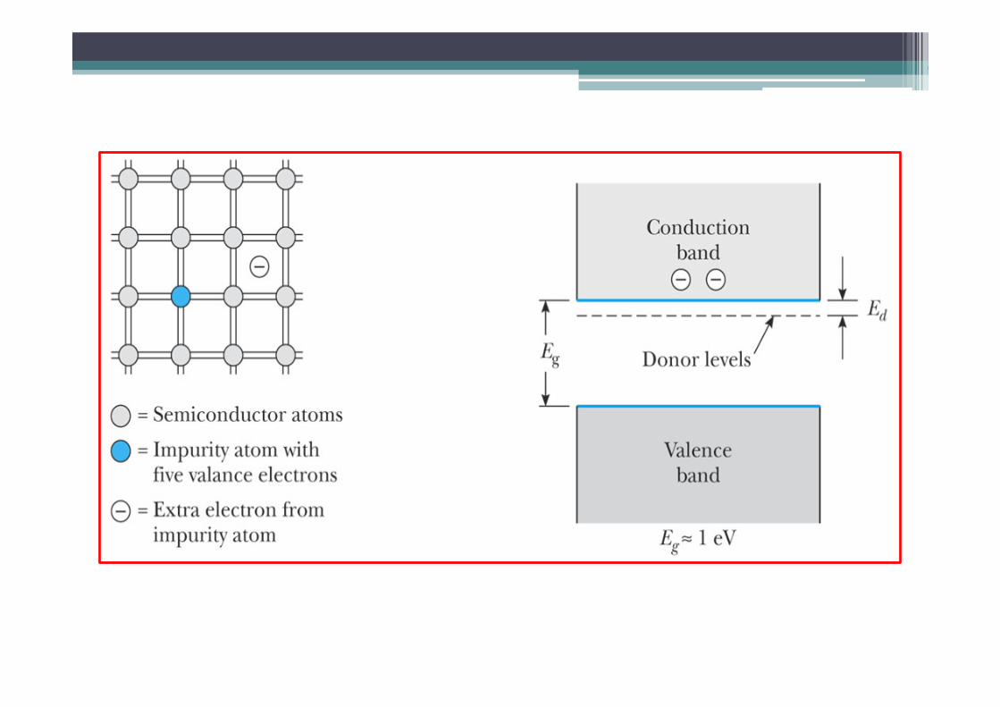
Donors: Energy Levels • The Band Structure View ▫ Such impurities “create” an energy level
within the band gap, close to the conduction band
• A donor is similar to a hydrogen atom ▫ A positive charge with a single electron
within its potential ▫ Such impurities are called hydrogenic
donors ▫ They create so-called “shallow” levels - the
levels that are very close to the conduction band, so the energy required to ionize the atom is small and a sizable fraction of donor atoms will be ionized at room temperature


The free electrons in n type silicon support the flow of current.
This crystal has been doped with a pentavalent impurity.

Acceptors • Use Silicon (Si) as an example ▫ Substitute one Group III atom (e.g. Al or In) with a Si (Group
IV) atom ▫ Si atoms have four valence electrons that participate in the
covalent bonding ▫ When a Group III atom replaces a Si atom, it cannot complete a
tetravalent bond scheme ▫ An “electronic vacancy” – hole – is formed when an electron
from the valence band is grabbed by the atom so that the core is negatively charged, the hole created is then attracted the negative core ▫ At T = 0 K this hole “stays” with atom – localized hole ▫ At T > 0 K, electron from the neighboring Si atom can jump
into this hole – the hole can then migrate and contribute to the current

Acceptors • At T > 0 K, electron from the
neighboring Si atom can jump into this hole – the hole starts to migrate, contributing to the current
• We can say that this impurity atom accepted an electron, so we call them Acceptors
• Acceptors accept electrons, but “donate” free holes

Acceptors • By “incorporating” the electron into the impurity atom we can
represent this (T = 0 K) as a negative charge in the core with a positive charge (hole) outside the core attracted by its [Coulomb] potential
• At T > 0 K this hole can be ionized • Such semiconductors are called p-type semiconductors since
they contribute positive charge carriers

Acceptor: Energy Levels • From the Band Structure View ▫ Such impurities “create” energy levels within the band gap, close to
the valence band ▫ They are similar to “negative” hydrogen atoms ▫ Such impurities are called hydrogenic acceptors ▫ They create “shallow” levels - levels that are very close to the
valence band, so the energy required to ionize the atom (accept the electron that fills the hole and creates another hole further from the substituted atom) is small


This crystal has been doped with a trivalent impurity.
The holes in p type silicon contribute to the current.
Note that the hole current direction is opposite to electron current so the electrical current is in the same direction


Carrier Concentrations in Extrinsic Semiconductors • The carrier densities in extrinsic semiconductors can be
very high • It depends on doping levels ([net] dopant concentration)
and ionization energy of the dopants • Often both types of impurities are present ▫ If the total concentration of donors (ND) is larger than the total
concentration of acceptors (NA) have an n-type semiconductor ▫ In the opposite case have a p-type semiconductor

Charge Neutrality Equation • To calculate the charge concentration, the charge
neutrality condition is used, since the net charge in a uniformly doped semiconductor is zero ▫ Otherwise, there will be a net flow of charge from one point to
another resulting in current flow
▫ p is the concentration of holes in the valence band ▫ n is the electron concentration ▫ ND
+ is the ionized donor concentration
▫ NA- is the ionized acceptor concentration

Resistivity of Semiconductors
• The carrier concentration and thus the conductivity is dominated by its essentially exponential dependence on temperature
• For intrinsic semiconductors
• For impurity semiconductors
• EF is first between the impurity level and the band edge and then approaches Eg/2 after most of the impurities are ionized

Optical Properties
• If semiconductor or insulator does not have many impurity levels in the band gap, photons with energies smaller than the band gap energy can’t be absorbed ▫ There are no quantum states with energies in the band gap
• This explains why many insulators or wide band gap semiconductors are transparent to visible light, whereas narrow band semiconductors (Si, GaAs) are not

Optical Properties
• Some applications ▫ Emission: light emitting diode (LED) and Laser Diode (LD) ▫ Absorption: Filtering
Sunglasses Si filters: transmission of infra red light with simultaneous blocking of
visible light

Optical Properties
• If there are many impurity levels the photons with energies smaller than the band gap energy can be absorbed, by exciting electrons or holes from these energy levels into the conduction or valence band, respectively ▫ Example: Colored Diamonds

Photoconductivity
• Charge carriers (electrons or holes or both) created in the corresponding bands by absorbed light can also participate in current flow, and thus should increase the current for a given applied voltage, i.e., the conductivity increases
• This effect is called Photoconductivity

Photoconductivity • Important Applications (Garcia 26.6) ▫ Night vision systems imaging IR radiation ▫ Solar cells ▫ Radiation detectors ▫ Photoelectric cells (e.g., used for automatic doors) ▫ Xerography ▫ CCD (“Digital Cameras”)

n-type
p-type
ND
NA
PN Junctions: Overview • The most important device is a junction between a
p-type region and an n-type region • When the junction is first formed, due to the
concentration gradient, mobile charges transfer near junction
• Electrons leave n-type region and holes leave p-type region
• These mobile carriers become minority carriers in new region (can’t penetrate far due to recombination)
• Due to charge transfer, a voltage difference occurs between regions
• This creates a field at the junction that causes drift currents to oppose the diffusion current
• In thermal equilibrium, drift current and diffusion must balance
− − − − − −
+ + + + +
+ + + + + + + + + +
− − − − − − − − − − − − −
V +

Diffusion • Diffusion occurs when there exists a
concentration gradient • In the figure below, imagine that we fill the left
chamber with a gas at temperate T • If we suddenly remove the divider, what
happens? • The gas will fill the entire volume of the new
chamber. How does this occur?

Diffusion (cont)
• The net motion of gas molecules to the right chamber was due to the concentration gradient
• If each particle moves on average left or right then eventually half will be in the right chamber
• If the molecules were charged (or electrons), then there would be a net current flow
• The diffusion current flows from high concentration to low concentration:

Total Current and Boundary Conditions • When both drift and diffusion are present, the
total current is given by the sum:
• In resistors, the carrier is approximately uniform and the second term is nearly zero
• For currents flowing uniformly through an interface (no charge accumulation), the field is discontinous

Carrier Concentration and Potential • In thermal equilibrium, there are no external
fields and we thus expect the electron and hole current densities to be zero:

Carrier Concentration and Potential (2) • We have an equation relating the potential to the
carrier concentration
• If we integrate the above equation we have
• We define the potential reference to be intrinsic Si:

Carrier Concentration Versus Potential
• The carrier concentration is thus a function of potential
• Check that for zero potential, we have intrinsic carrier concentration (reference).
• If we do a similar calculation for holes, we arrive at a similar equation
• Note that the law of mass action is upheld

The Doping Changes Potential • Due to the log nature of the potential, the potential
changes linearly for exponential increase in doping:
• Quick calculation aid: For a p-type concentration of 1016 cm-3, the potential is -360 mV
• N-type materials have a positive potential with respect to intrinsic Si

PN Junction Currents • Consider the PN junction in thermal equilibrium • Again, the currents have to be zero, so we have
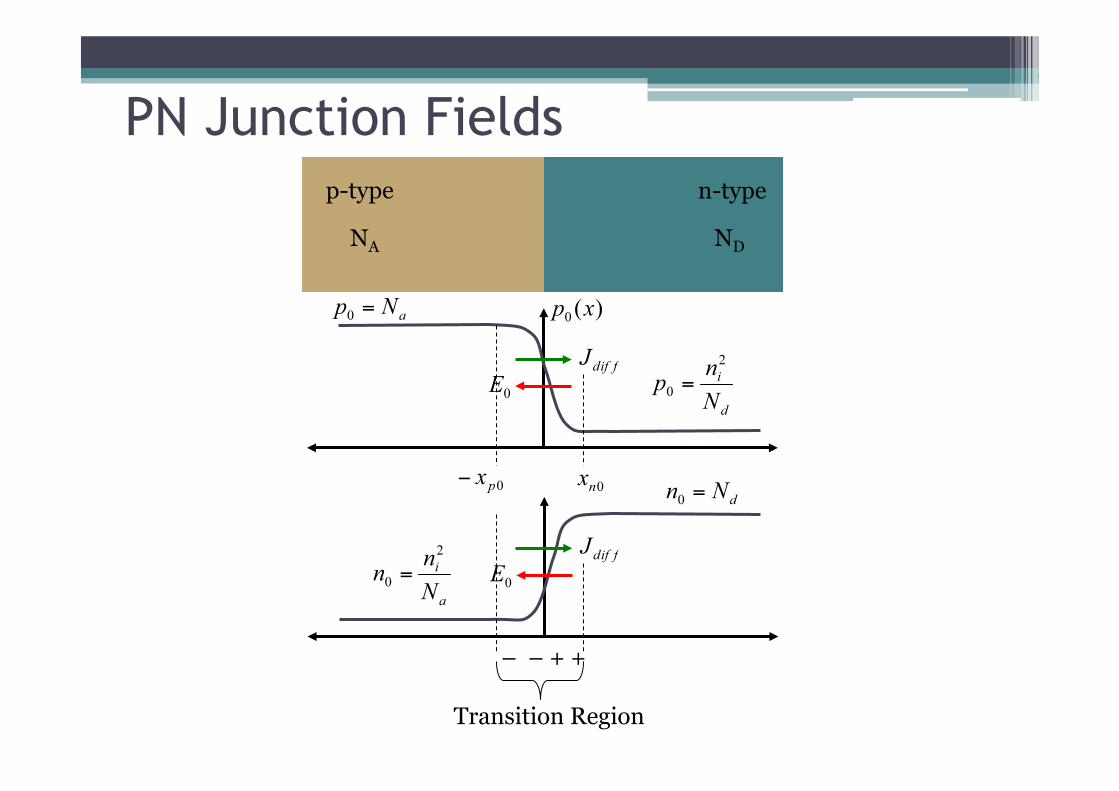
PN Junction Fields n-type p-type
ND NA
Transition Region
– – + +

Total Charge in Transition Region • To solve for the electric fields, we need to write
down the charge density in the transition region:
• In the p-side of the junction, there are very few electrons and only acceptors:
• Since the hole concentration is decreasing on the p-side, the net charge is negative:
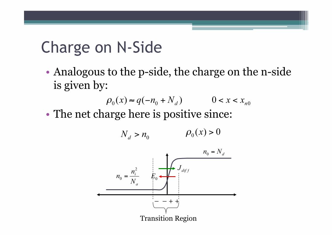
Charge on N-Side • Analogous to the p-side, the charge on the n-side
is given by:
• The net charge here is positive since:
Transition Region
– – + +

“Exact” Solution for Fields • Given the above approximations, we now have an
expression for the charge density
• We also have the following result from electrostatics
• Notice that the potential appears on both sides of the equation… difficult problem to solve
• A much simpler way to solve the problem…

Depletion Approximation • Let’s assume that the transition region is
completely depleted of free carriers (only immobile dopants exist)
• Then the charge density is given by
• The solution for electric field is now easy
Field zero outside transition region

Depletion Approximation (2) • Since charge density is a constant
• If we start from the n-side we get the following result
Field zero outside transition region

Plot of Fields In Depletion Region
• E-Field zero outside of depletion region • Note the asymmetrical depletion widths
n-type p-type
ND NA
– – – – – – – – – – – – – – – – – – – –
+ + + + +
+ + + + +
+ + + + +
+ + + + +
Depletion Region

Continuity of E-Field Across Junction • Recall that E-Field diverges on charge. For a
sheet charge at the interface, the E-field could be discontinuous
• In our case, the depletion region is only populated by a background density of fixed charges so the E-Field is continuous
• What does this imply?
• Total fixed charge in n-region equals fixed charge in p-region! Somewhat obvious result.

Potential Across Junction • From our earlier calculation we know that the
potential in the n-region is higher than p-region • The potential has to smoothly transition form
high to low in crossing the junction • Physically, the potential difference is due to the
charge transfer that occurs due to the concentration gradient
• Let’s integrate the field to get the potential:

Potential Across Junction • We arrive at potential on p-side (parabolic)
• Do integral on n-side
• Potential must be continuous at interface (field finite at interface)

Solve for Depletion Lengths • We have two equations and two unknowns. We
are finally in a position to solve for the depletion depths
(1)
(2)

Sanity Check • Does the above equation make sense? • Let’s say we dope one side very highly. Then
physically we expect the depletion region width for the heavily doped side to approach zero:
• Entire depletion width dropped across p-region

Total Depletion Width • The sum of the depletion widths is the “space
charge region”
• This region is essentially depleted of all mobile charge
• Due to high electric field, carriers move across region at velocity saturated speed

Have we invented a battery? • Can we harness the PN junction and turn it into
a battery?
• Numerical example:
?

Contact Potential • The contact between a PN junction creates a
potential difference • Likewise, the contact between two dissimilar
metals creates a potential difference (proportional to the difference between the work functions)
• When a metal semiconductor junction is formed, a contact potential forms as well
• If we short a PN junction, the sum of the voltages around the loop must be zero:
p n +
−

Diode under Thermal Equilibrium
• Diffusion small since few carriers have enough energy to penetrate barrier • Drift current is small since minority carriers are few and far between: Only
minority carriers generated within a diffusion length can contribute current • Important Point: Minority drift current independent of barrier! • Diffusion current strong (exponential) function of barrier
p-type n-type - - -
-
- - -
- - - - - -
+ + + + + + + + + + + + +
−
−
+
+
−
−
Thermal Generation
Recombination Carrier with energy below barrier height
Minority Carrier Close to Junction

Reverse Bias Reverse Bias causes an increases barrier to
diffusion Diffusion current is reduced exponentially
Drift current does not change Net result: Small reverse current
p-type n-type - - - -
- - -
+ + + + + + + +
−

Forward Bias Forward bias causes an exponential increase in
the number of carriers with sufficient energy to penetrate barrier
Diffusion current increases exponentially
Drift current does not change Net result: Large forward current
p-type n-type - - - -
- - -
+ + + + + + + +
−

Diode I-V Curve
• Diode IV relation is an exponential function • This exponential is due to the Boltzmann distribution of carriers
versus energy • For reverse bias the current saturations to the drift current due to
minority carriers

Minority Carriers at Junction Edges
Minority carrier concentration at boundaries of depletion region increase as barrier lowers … the function is
(minority) hole conc. on n-side of barrier
(majority) hole conc. on p-side of barrier
(Boltzmann’s Law)
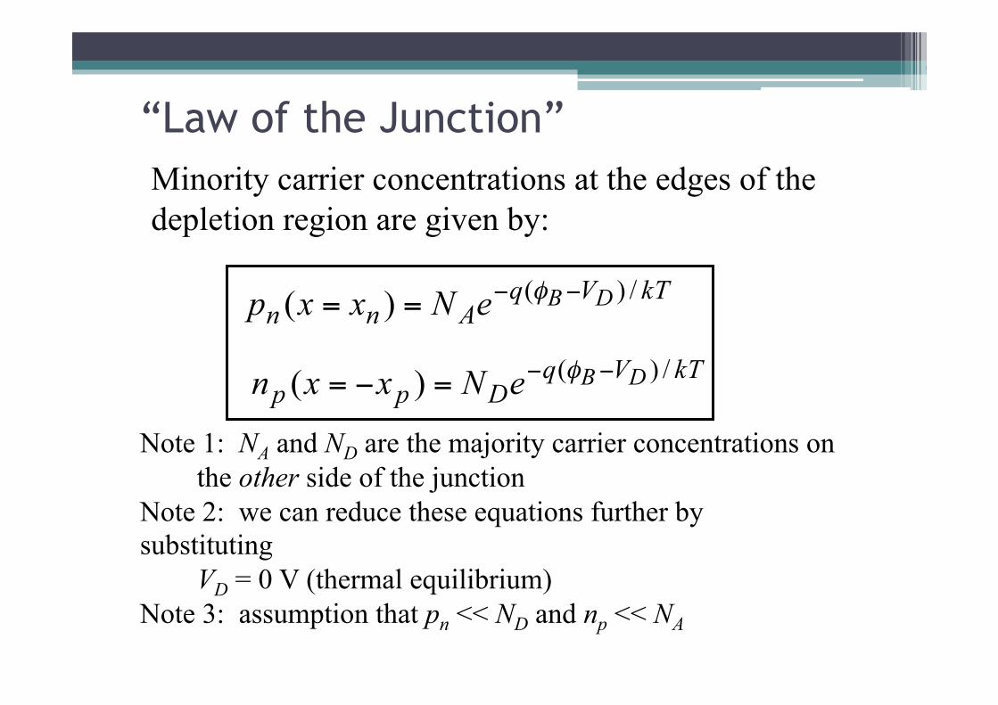
“Law of the Junction” Minority carrier concentrations at the edges of the depletion region are given by:
Note 1: NA and ND are the majority carrier concentrations on the other side of the junction
Note 2: we can reduce these equations further by substituting
VD = 0 V (thermal equilibrium) Note 3: assumption that pn << ND and np << NA
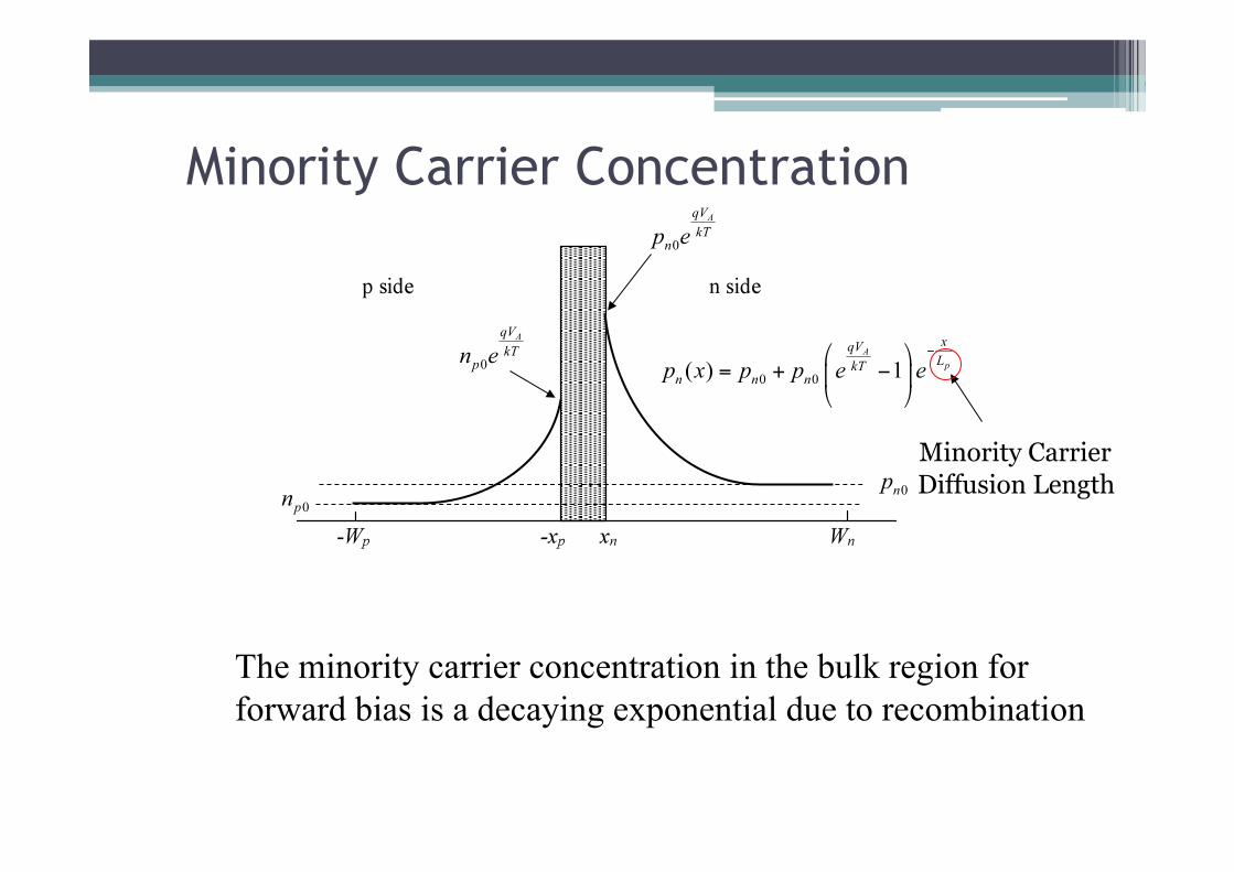
Minority Carrier Concentration
The minority carrier concentration in the bulk region for forward bias is a decaying exponential due to recombination
Minority Carrier Diffusion Length

Steady-State Concentrations Assume that none of the diffusing holes and electrons recombine get straight lines …
This also happens if the minority carrier diffusion lengths are much larger than Wn,p

Diode Current Densities

Diode Circuits
• Rectifier (AC to DC conversion) • Average value circuit • Peak detector (AM demodulator) • DC restorer • Voltage doubler / quadrupler /…