Embed Size (px)
Citation preview


KINKENResearch Highlights
Institute for Materials Research,Tohoku University
2013
1986. FebruaryCourtesy of Tohoku University Historical Museum.

KINKEN Research Highlights 2013Contents
Preface 1
Research Highlights
1. Infrastructural Materials
Microstructure Design of Structural Metallic Materials Division 3
Chemical Physics of Non-Crystalline Materials Division 5
Biomaterials Science Division 7
Crystal Chemistry Division 9
Deformation Processing Division 11
Advanced Analysis of Materials Division 13
Computational Materials Research Initiative 15
2. Energy-related Materials
Surface and Interface Research Division 17
Metal Physics with Quantum Beam Spectroscopy Division 19
Physics of Crystal Defects Division 21
Materials Design by Computer Simulation Division 23
Nuclear Materials Science Division 25
Nuclear Materials Engineering Division 27
Non-Equilibrium Materials Division 29
Hydrogen Functional Materials Division 31
Advanced Crystal Engineering Laboratory 33
Analytical Science Division 35

3. Electronic Materials
Theory of Solid State Physics Division 37
Magnetism Division 39
Low Temperature Condensed State Physics Division 41
Irradiation Effects in Nuclear and Their Related Materials Division 43
Physics of Electronic Materials Division 45
Magnetic Materials Division 47
Multi-Functional Materials Science Division 49
Radiochemistry of Metals Division 51
Materials Processing and Characterization Division 53
Advanced Materials Development and Integration of Novel Structured Metallic and Inorganic Materials 55
Research Centers
International Research Center for Nuclear Materials Science 57
Cooperative Research and Development Center for Advanced Materials
(Formerly Advanced Research Center of Metallic Glasses) 59
High Field Laboratory for Superconducting Materials 61
Kansai Center for Industrial Materials Research 63
Center for Computational Materials Science 65
International Collaboration Center (ICC-IMR) 67
Integrated Materials Research Center for a Low-Carbon Society(LC-IMR) 69
Center of Neutron Science for Advanced Materials 71
Laboratory of Low Temperature Materials Science 73
Laboratory of alpha-Ray Emitters 75
Analytical Research Core for Advanced Materials 77
Research and Development Center for Ultra High Efficiency Nano-crystalline Soft Magnetic Material 79
Author Index 82
Keyword Index 83

1 IMR KINKEN Research Highlights 2013 IMR KINKEN Research Highlights 2013
Preface
Dear colleagues,
Professor Kotaro Honda established a steel research organization officially known as “the 2nd
Division of the Provisional Institute of Physical and Chemical Research” at Tohoku University in 1916 In
1987, the organization was restructured into its present form as a national collaborative research institute
affiliated to Tohoku University and was consequently renamed “the Institute for Materials Research”
(IMR), also known as “KINKEN” (which is the short form for “kinzoku zairyo kenkyujo,” the Japanese
name for IMR)
Since its establishment, IMR has become known for its excellence in both fundamental and applied
research on metals and on a wide range of new materials Numerous functional materials have been
studied and developed at IMR, including Kichizaemon Sumitomo (KS) magnetic steel, new KS magnetic
steel, SiC fibers, compound alloys, metallic glasses, and others
IMR has greatly contributed to the advancement of materials science As one example, our study of
magnetism resulted in the invention of the world’s strongest permanent magnet, the KS magnet, which
dramatically improves the performance of electrical machines IMR has historically focused on
fundamental research to develop applications for a wide range of advanced technologies More recently,
IMR has developed a wide array of materials including high-performance, high-quality, and multifunctional
materials such as amorphous alloys, bulk metallic glasses, intermetallic compounds, quasicrystals,
oxides, ceramics, nanostructured Si and Ge, optical and electronic materials, solar cell crystals,
biomaterials, organic materials, hydrogen storage alloys, shaped crystals, and III-V, II-VI, and oxide
semiconductors

IMR KINKEN Research Highlights 2013 2IMR KINKEN Research Highlights 2013
Director
IMR has completely recovered from the Great East Japan Earthquake that occurred on March 11,
2011, and we are working hard to achieve innovative research and development in the fields of materials
science and engineering KINKEN will celebrate its 100th anniversary on May 21, 2016 We would like to
introduce the logo for KINKEN’s 100th anniversary, which has been selected from among 726 candidates
We have redefined our missions and are establishing new roles for KINKEN in the post 3/11 era
We are pleased to introduce KINKEN Research Highlights 2013, the seventh annual report containing
a collection of the research output during the previous year at KINKEN We decided in 2007 to annually
prepare this report so that our colleagues around the world can be kept informed about our research
activities The studies conducted at our individual research laboratories and research centers and those
jointly conducted with other academic institutions are provided, especially those in the key research
fields of infrastructural, energy-related, and electronic materials
The world faces serious issues such as the deterioration of the environment and the depletion of
natural resources and nonrenewable energy sources IMR will promote research into materials to further
address the problems associated with these issues with the aims of sustaining human development and
ensuring a high standard of living for all people In this way, we can offer a brighter future to subsequent
generations
We hope that the KINKEN Research Highlights will enable you to better understand and support our
research activities and will aid the promotion of worldwide collaboration with our institute in the field of
materials research We ask for your continued support and welcome any suggestions

Infrastructural Materials
3 IMR KINKEN Research Highlights 2013 IMR KINKEN Research Highlights 2013
IntroductionIt is well known that ferrite-martensite dual
phase (DP) steels exhibit high strength and good formability and has widely been in practical use [1]. Stress-strain curves of ferrite-martensite DP steels are characterized by large work-hardening and uniform elongation but small post-uniform elongation. On the other hand, interphase precipitated steels, composed of single phase ferrite and dispersion of nano-sized alloy carbides in ferrite, are also known as commercial steels having a good balance of high strength and formability [2]. Stress-strain curves of interphase precipitated steels are such that work hardening and uniform elongation are relatively low but post-uniform elongation is quite large [3]. That is, ferrite-martensite DP steels and interphase precipitated steels have both good and bad points. It may be possible to significantly improve the strength and ductility if nano-sized alloy carbides are dispersed in ferrite phase of ferrite-martensite DP steels, combining advantages of both steels, which is a motivation for the present study.
In this study, ferrite-martensite DP samples with dispersion of nano-sized vanadium carbides (VC) in ferrite phase were produced using ferrite transformation accompanied with interphase precipitation followed by water quenching in a V-added low carbon steel, and the mechanical properties of such DP samples were systematically investigated to understand the effect of nano-sized precipitates on the strength and ductility of DP steels.
ExperimentalA low carbon steel with a chemical composition
of Fe-0.095%C-1.49%Mn-0.43%V (in mass%) (V-added steel) was used in the present study. After austenitizing at 1100oC for 600 s, samples were isothermally transformed at 690oC for different holding periods followed by quenching, leading to ferrite-martensite DP samples accompanied with interphase precipitation of VC in ferrite. Conventional ferrite-martensite DP samples with no VC particles were also prepared using Fe-0.098%-1.5%Mn (V-free steel) for comparison. Microstructures were characterized by optical microscopy, transmission electron microscopy (TEM) and electron backscatter diffraction (EBSD). Tensile tests were carried out at room temperature at an initial strain rate of 8.3 x 10⁻⁴ s-1.
Results and DiscussionBy using isothermal ferrite transformation
followed by water quenching, ferrite-martensite DP samples with different volume fraction of ferrite has successfully been obtained for both V-added and V-free steels. TEM observation has confirmed that VC precipitates with an average diameter of approximately 10 nm were distributed in ferrite phase of V-added DP samples. Tensile tests were carried out for the obtained DP samples, and strength and elongation were determined from stress-strain curves. Fig. 1 shows the strength and ductility of the samples as a function of volume fraction of ferrite. It is seen that the strength of
Mechanical Properties of Ferrite-martensite Dual Phase Steels with Interphase PrecipitationFerrite-martensite dual phase steels with interphase precipitation of nano-sized vanadium carbides were prepared and mechanical properties were systematically investigated. It was found that nano-sized vanadium carbides are effective for improving the post-uniform elongation as well as increasing the strength of dual phase steels.
Fig. 1 Strength and ductility of V-free and V-added steels. (a) 0.2% proof stress and ultimate tensile strength, (b) uniform elongation and (c) post-uniform elongation.

Infrastructural Materials
IMR KINKEN Research Highlights 2013
IMR KINKEN Research Highlights 2013
4IMR KINKEN Research Highlights 2013
V-added DP samples is higher than that of V-free DP samples, which should be due to precipitation strengthening of ferrite by nano-sized VC particles. Uniform elongation of the samples decreases by addition of vanadium, but post-uniform elongation is slightly larger in the V-added DP samples than that in the V-free samples.
Strength-ductility balance is compared between V-added and V-free samples in Fig. 2. The balance of ultimate tensile strength and uniform elongation in Fig. 2a shows that the balance curve is shifted toward high-strength and low-ductility region by V addition, but the balance of both V-added and V-free samples are located in the single curve. This result indicates that V addition increases the strength of DP samples with keeping a good balance of ultimate tensile strength and uniform elongation. On the other hand, it is clearly seen that V addition improves the balance of strength and post-uniform elongation in the DP samples.
To understand the difference in the mechanical properties of the DP samples between V-free and V-added steels, the work hardening behavior was compared. It was found that the work hardening rate during tensile test for ferrite-martensite DP samples decreases by addition of VC. This can explain the reason why the uniform elongation decreased by addition of V. However, this result is somewhat surprising since nano-sized alloy carbides are reported to have an effect to increase the working hardening in the tensile test of single phase ferrite steels [3]. To further understand the mechanisms behind, digital image correlation (DIC)
analysis was applied to investigate the strain distribution introduced in the DP samples during tensile tests. The DIC analysis revealed the following results. In the V-free steel, strain distribution was quite heterogeneous, and in particular the strain was more concentrated on soft ferrite phase. However, it was clearly shown that the strain distribution became more uniform in the V-added steel. These tendencies suggest that precipitation strengthening of ferrite by VC particles reduces the difference in strength between ferrite and martensite phase in DP samples, which would suppress inhomogeneous deformation during the tensile test. This corresponds well with the decreased work hardening and smaller uniform elongation in the V-added DP samples. More homogeneous deformation caused by VC dispersion may also suppress formation of voids or cracks in the later stage of tensile deformation. This would be the reason why the V addition led to an increase in the balance of strength and post-uniform elongation. It can be suggested that nano-sized alloy carbides are effective for improving the post-uniform elongation as well as increasing the strength of DP steels.
References[1] “Fundamentals of Dual Phase Steels”, edited by R. A. Kot and
B. L. Bramfitt, AIME, (1981).
[2] Y. Funakawa, T. Shiozaki, K. Tomita, T. Yamamoto, and E.
Maeda: ISIJ International, 44, 1945-1951(2004).
[3] N. Kamikawa, Y. Abe, G. Miyamoto, Y. Funakawa, and T.
Furuhara: Tetsu-to-Hagané, 99, 352-361(2013).
Keywords: steel, mechanical properties, deformationTadashi Furuhara, Goro Miyamoto, and Naoya Kamikawa (Microstructure Design of Structural Metallic Materials Division)E-mail: [email protected]: http://www.st-mat.imr.tohoku.ac.jp
Fig. 2 Strength-ductility balance of V-free and V-added steels. (a) Ultimate tensile strength vs uniform elongation and (b) ultimate tensile strength vs post-uniform elongation.

Infrastructural Materials
5 IMR KINKEN Research Highlights 2013 IMR KINKEN Research Highlights 2013
Chrysocolla, Cu2H2(Si2O5)(OH)4∙nH2O, is a secondary mineral that forms in the oxidized zones of copper deposits (Fig. 1). Because of the unique Cu/Si molar ratio for natural chrysocolla, it is reasonable to assume that the production of natural chrysocolla is associated with a regular chemical reaction during sedimentation from solutions containing copper and silica components, and understanding the mechanism of the mineralization of chrysocolla is expected to provide useful information on its cryptocrystalline structure. This prompted us to study the disordered structure of a synthetic analogue of chrysocolla prepared using the sol-gel method [1].
The sol-gel method and reagents CuSO4∙5H2O and Si(OC2H5)4 (TEOS) were used to prepare hydrated copper silicate gels with three different Cu/Si molar compositions. The Cu/Si molar ratios for the three obtained gel samples were 0.32, 0.83, and 1.61 (hereafter named Cu1Si2, Cu1Si1, and Cu2Si1, respectively).
The thermogravimetric (TG) curves for Cu1Si2, Cu1Si1, Cu2Si1, and natural chrysocolla show relatively smooth weight losses of 19.0, 22.0, 24.3, and 20.2%, respectively. The differential thermal analysis (DTA) curves for Cu1Si1 and natural chrysocolla show exothermic peaks at ~680°C, which correspond to thermal decomposition during the formation of crystalline CuO. Although exothermic peaks are not clearly shown in of the DTA curves for
Cu1Si2 and Cu2Si1, evidence of a similar reaction associated with the formation of CuO was found by heating Cu1Si2 and Cu2Si1 at 1000°C. This thermal behavior is different from that observed for Cu(OH)2 (spertiniite). Therefore, each of the synthetic gel samples is not a simple assemblage of spertiniite and amorphous or crystalline silica but it also includes a substance similar to natural chrysocolla.
The X-ray diffraction (XRD) patterns for the three gel samples and for natural chrysocolla are shown in Fig. 2. Each pattern consists of a few diffuse maxima, and several broad peaks are superimposed on them. The profiles for Cu1Si2 and Cu1Si1 indicate broad peaks at Q = 3.8, 4.2, and 4.6 Å-1, which correspond well with those for natural chrysocolla. In particular, the XRD pattern for Cu1Si1 is quite similar to that for natural chrysocolla, suggesting the Cu1Si1 gel is isostructural with natural chrysocolla. The first diffuse maximum in the XRD pattern for Cu1Si2, on the other hand, is attributed to the structure of ordinary amorphous SiO2. This feature enables us to consider that part of the SiO2 in Cu1Si2 is encouraged to form amorphous SiO2.
Fig. 3 shows the reduced distribution functions (RDFs) for the Cu1Si2, Cu1Si1, and Cu2Si1 samples and for SiO2 glass and natural chrysocolla. The atomic correlation peaks for every pair of constituents
Structure of Hydrated Copper silicate gelsHydrated copper silicate gel samples were prepared using the conventional sol-gel method and stock solutions whose Cu/Si molar ratios were different. The structures of the obtained gel samples were analyzed using X-ray diffraction and extended X-ray absorption fine structure (EXAFS) spectroscopy. A common medium-range structure similar to that of natural chrysocolla was produced in each gel sample. The local structure of chrysocolla is readily produced in during sedimentation from any solutions containing CuO and SiO2 components.
Fig. 1 Chrysocolla from Chuquicamata, Chile.
Fig. 2 X-ray diffraction patterns of three gel samples. The pattern of chrysocolla from Chuquicamata, Chile and SiO2 glass are also shown.

Infrastructural Materials
IMR KINKEN Research Highlights 2013
IMR KINKEN Research Highlights 2013
6IMR KINKEN Research Highlights 2013
are clearly observed up to ~15 Å for Cu2Si1, Cu1Si1, Cu1Si2 and natural chrysocolla. However, the atomic correlation for SiO2 glass becomes less distinct with increasing radial distance and disappears over 10 Å. Since the oscillations in the reduced RDFs well represent the degree of structural ordering, the obtained Cu1Si2, Cu1Si1, and Cu2Si1 gel samples show structures whose middle-range orderings are different from those for common glasses. The dashed lines in Fig. 3 indicate the atomic distances for the Si-O bonds in the tetrahedral unit and the Cu-O bonds in the square planar unit, respectively. The first nearest-neighbor correlation for each gel represents a harmonization of the Si-O and Cu-O correlations and suggests the existence of the SiO4 unit.
Fig. 4 shows Cu K-edge extended X-ray absorption fine structure EXAFS χ(k) functions for the synthetic gel samples and for natural chrysocolla. The spectra for Cu1Si2, Cu1Si1, and natural chrysocolla feature oscillation peaks at k = 7.5 and 10 Å-1, while those peaks are absent in the spectrum for Cu2Si1. This result indicates that the local structures around Cu in Cu1Si2 and Cu1Si1 are similar to that of natural chrysocolla and that Cu2Si1 has a unique Cu environment.
Copper silicate gels were synthesized through sol-gel precipitation from starting materials whose Cu/Si molar ratios were different. The TG-DTA, XRD, and EXAFS measurements indicated that middle-
range ordering similar to that of natural chrysocolla was formed in each of the gel samples despite the variation in the Cu/Si molar ratio of the starting stock solutions. In particular, the structural feature of the Cu1Si1 gel sample is equivalent to that of natural chrysocolla. Therefore, the nearly stoichiometric composition of cryptocrystalline chrysocolla strongly associates with its short- and medium-range order, and this unique ordering is formed as a result of a chemical reaction during precipitation from solutions containing SiO2 and CuO components. The local structural information about the CuO4 units around Cu together with the common SiO4 units observed in the Cu1Si1 gel and natural chrysocolla enables us to consider middle-range ordering such as that found in crystalline dioptase (CuSiO3∙H2O) and planchéite. However, the linkages of the CuO4 and SiO4 units in chrysocolla are still unknown. Further systematic investigation with methods such as high-energy X-ray diffraction is strongly required in order to obtain high-resolution pair distribution function data.
References[1] T. Hariu, H. Arima, and K. Sugiyama, J. Mineral. Petrol. Sci.,
108, 111-115 (2013).
Keywords: cryptocrystalline, pair distribution function, XAFSHiroshi Arima, Kazumasa Sugiyama (Chemical Physics of Non-Crystalline Materials Division)E-mail: [email protected], [email protected]: http://www.xraylab.imr.tohoku.ac.jp/
Fig. 3 Reduced atomic pair distribution functions of the gels, chrysocolla from Chuquicamata, Chile, and SiO2 glass
Fig. 4 Cu K-edge k2-weighted X(k) functions of the gels and chrysocolla from Chuquicamata, Chile.

Infrastructural Materials
7 IMR KINKEN Research Highlights 2013 IMR KINKEN Research Highlights 2013
In biomedical applications, bone absorption and degradation of bone quality are induced by stress shielding resulting from mismatch between the Young’s moduli of living bone tissue and implant devices. Therefore, a β-type Ti alloy, Ti-29Nb-13Ta-4.6Zr (mass%, TNTZ) [1], has been developed with a low Young’s modulus to overcome this significant problem. The Young’s modulus of TNTZ is approximately 60 GPa [1], which is much closer to that of cortical bone (10–30 GPa) than to those of existing Ti alloys. However, Ti and its alloys fuse with bone through fibrous tissues, and it takes a long time for them to do so[2]. Therefore, it is necessary to improve the hard-tissue compatibility of TNTZ.
A coating of hydroxyapatite (Ca10(PO4)6OH2; HAp) is very effective in improving the hard-tissue
compatibility of Ti and its alloys. HAp directly bonds with bone tissue without any fibrous cells forming. In the present study, two methods were used to form HAp on TNTZ in order to improve the hard-tissue compatibility of TNTZ.
The first method of forming HAp on the TNTZ surface is alkali treatment. HAp forms on the surfaces of pure Ti and its alloys immersed in a NaOH solution and then in simulated body fluid (SBF) whose ion concentrations are almost the same as those in the human body. However, the HAp formability of TNTZ soaked in SBF after alkali treatment is lower than that of pure Ti that has been subjected to the same treatment conditions. Therefore, it is important to understand the relation between the alloying elements Nb, Ta, and Zr and HAp formability in order to improve the HAp formability of TNTZ. In this study, the HAp formability of Ti-xM (nominal content x = 10, 20, 30, or 40 mass%; M = Nb, Ta, or Zr) and of each pure metal soaked in SBF after alkali treatment was investigated [3].
Fig. 1 shows scanning electron microscope (SEM) images of the surfaces of (a) Ti-xNb and pure Nb, (b) Ti-xTa and pure Ta, and (c) Ti-xZr and pure Zr soaked in SBF for 1 week after alkali treatment in 1 M NaOH solution at 363 K for 259.2 ks [3]. The HAp coverage on the Ti-xTa surfaces is almost constant at ~95%; however, the coverage on the Ti-xNb and Ti-xZr surfaces decreased from 90–95% to 0% as the Nb and Zr contents increased from 10 to 100 mass% (i.e., pure Nb and Zr metals).
The X-ray diffraction (XRD) profiles for the alkali-treated Ti-xTa showed that Na2Ti5O11 and Na5TaO5 had formed on the surfaces (data not shown here) [3]. The XRD profiles for the alkali-treated Ti-xNb and Ti-xZr, on the other hand, showed that only Na2Ti5O11 had formed on the surfaces (data not shown here) [3]. The Ti-Nb and Ti-Zr alloys showed good HAp formability when the Nb and Zr contents were lower than 10 mass% because enough sodium titanate was present on the surfaces. However, when the Nb or Zr content was increased to 20 mass%, the number of Ti atoms on the surfaces decreased, resulting in a
Improvement in Hard-Tissue Compatibility of β-type Titanium Alloy by Formation of Hydroxyapatite through Alkali Treatment and Metal Organic Chemical Vapor DepositionThe hard-tissue compatibility of the β-type Ti alloy Ti-29Nb-13Ta-4.6Zr (TNTZ) was improved using two methods. The effects of the alloying elements Ta, Nb, and Zr on the hydroxyapatite (HAp) formability of Ti alloys soaked in simulated body fluid after alkali treatment were investigated to improve the formability of HAp on TNTZ-based implants for the human body. Furthermore, the adhesive strengths of HAp films deposited through metal organic chemical vapor deposition onto TNTZ substrates were improved by controlling surface morphology of TNTZ substrates.
Fig. 1 SEM images of Ti-xM (nominal content x = 10, 20, 30, or 40 mass%; M = Nb, Ta, or Zr) alloy and each pure metal soaked in SBF for 1 week after alkali treatment in 1 M NaOH solution at 363 K for 259.2 ks.

Infrastructural Materials
IMR KINKEN Research Highlights 2013
IMR KINKEN Research Highlights 2013
8IMR KINKEN Research Highlights 2013
decrease in the sodium titanate content on the surfaces. These results suggest that the sodium titanate and sodium tantalate on the surfaces were responsible for HAp nucleation. Therefore, it is important to maximize the formation of sodium titanate and sodium tantalate on the TNTZ surface in order to improve the hard-tissue compatibility of TNTZ.
The second method of forming HAp on the TNTZ surface is dry coating; namely, metal organic chemical vapor deposition (MOCVD), which is a useful method of coating HAp films onto metal surfaces. This study was undertaken with the aim of improving the adhesive strength of HAp films deposited onto TNTZ substrates through MOCVD by optimizing the surface morphology; i.e., the surface roughness and size of asperities of the TNTZ substrates [4].
Fig. 2 shows atomic force microscopy (AFM) images and surface roughness (Ra) values for TNTZ substrates with a mirror-like surface finish and for those polished with #1000-, #1500-, and #2400-grit abrasive papers [4]. The surfaces of the TNTZ substrate with a mirror-like finish and that polished with #2400-grit abrasive paper are relatively smooth. The surfaces of the TNTZ substrates polished with #1500- and #1000-grit abrasive papers, on the other hand, are uniformly rough and show nanoasperities. Microasperities are also observed on the surface of the TNTZ substrate polished with
the #1000-grit abrasive paper. Fig. 3 shows the adhesive strengths of the HAp
films deposited onto the TNTZ substrate with a mirror-like surface finish and onto those whose surfaces were polished with #1000-, #1500-, and #2400-grit abrasive papers [4]. The adhesive strength of the HAp film deposited onto the TNTZ substrate with a mirror-like surface finish is approximately 10 MPa. Mechanical polishing using #1000-, #1500-, and #2400-grit abrasive papers improved the adhesive strengths of the HAp films. The surface of the TNTZ substrate polished with the #1000-grit abrasive paper is rougher than that of the TNTZ substrate polished with the #1500-grit abrasive paper. However, the adhesive strengths of the HAp films deposited onto these two substrates are nearly equal. These results indicate that the nanoasperitie play a more important role in improving the adhesive strength of the HAp films than the surface roughness of the substrates does.
References[1] D. Kuroda, M. Niinomi, M. Morinaga, Y. Kato, and T. Yashiro,
Mater. Sci. Eng. A 243, 244 (1998).
[2] M. Niinomi, T. Hattori, K. Morikawa, T. Kasuga, A. Suzuki, H.
Fukui, and A. Niwa, Mater. Trans. 43, 2970 (2002).
[3] K. Cho, M. Niinomi, M. Nakai, J. Hieda, and X. Tao, Mater.
Trans. 54, 1295 (2013).
[4] J. Hieda, M. Niinomi, M. Nakai, K. Cho, T. Gozawa, H. Katsui,
R. Tu, and T. Goto, J. Mech. Behav. Biomed. Mater. 18, 232
(2013).
Keywords: biomedical, alloy, hydroxyapatiteMitsuo Niinomi ( Biomaterials Science Division)E-mail: [email protected]: http://biomat.imr.tohoku.ac.jp/
Fig. 2 AFM images of (a) TNTZ substrate surface with mirror-like finish and TNTZ substrates polished with (b) #2400-, (c) #1500-, and (d) #1000-grit abrasive papers.
Fig. 3 Adhesive strengths of HAp films deposited onto TNTZ substrate with mirror-like surface finish and TNTZ substrates subjected to mechanical polishing using #2400-, #1500-, and #1000-grit abrasive papers.

Infrastructural Materials
9 IMR KINKEN Research Highlights 2013 IMR KINKEN Research Highlights 2013
Colloidal crystals are a promising tool for investigating diverse basic physical phenomena. We applied a colloidal crystal to impurity partitioning because impurity partitioning is one of the most universal phenomena observed during the growth of crystals from melts, and it strongly affects the properties of bulk crystals. Since no research has previously been conducted on the impurity partitioning of colloidal crystals, this work investigates the detailed partitioning behaviors such as the growth rate, size of impurity particles, and types of impurities formed during colloidal crystallization [1].
A small amount of impurities (2%) was doped
into a colloidal dispersion from which colloidal crystals were grown. Various sizes of pure polystyrene (PS) particles (i.e., 300, 400, 600, and 700 nm) and fluorescent bearing (w/fluor.) particles (i.e., 300, 400, 520, 600, and 700 nm) were doped as impurity particles into the colloidal crystals.
Convective assembly [2] was used to grow the colloidal crystals. More than several tens of layers of colloidal crystals were formed on a glass plate (Fig. 1A). The cleavage surface was observed using scanning electron microscopy (SEM) to evaluate the concentrations of the impurity particles in the bulk. Most of the impurity particles had substituted for constituent particles, as shown in Fig. 1B.
The effective partition coefficient (keff) was measured at various growth rates (Fig. 1C) and for each size of each impurity particle. Keff approached unity with increasing growth rate for each sample. Further, the closer the size of the impurity particle was to that of the host particle, the easier it became for keff to approach unity. In addition, the keff values for the w/fluor. particles were larger than those for the pure PS particles for all particle sizes. It should also be noted that keff for the 520 nm w/fluor. particles surpassed unity.
Fig. 1D shows k0 obtained from keff by using BPS plot [3]. k0 decreased with increasing difference between the size of the impurity particle and the 500-nm host particle. k0 for each w/fluor. particle size was larger than that for the corresponding pure PS particle size. k0 surpassed unity for the 520-nm w/fluor. particle, whereas it was always less than unity for the PS particles.
We used a Thurmond and Struthers (T&S) model [4] to determine the difference between the k0 values for the PS and w/fluor. particles. The T&S model defines k0 as exp((ΔGTr–ΔH)/RT), where ΔGTr is the change in the Gibbs free energy of fusion; that is, the difference between the Gibbs free energies of the solid and liquid phases of an impurity at the
Impurity Partitioning During Colloidal CrystallizationColloidal crystal was used as a model of impurity partitioning during the growth of a bulk crystal. The detailed partitioning behavior of the colloidal crystal was investigated for the first time. The effective partition coefficient, keff (= CS/C0), was investigated for pure polystyrene and for polystyrene dyed with fluorescent particles by changing the ratio of the particle diameters, Dimp/Dcryst, and growth rate, V. keff was less than unity and increased to unity with increasing V for each size of polystyrene particles, whereas keff increased to unity as Dimp/Dcryst approached unity at a given growth rate. These results were consistent with the solute behavior analyzed using a Burton-Prim-Slichter (BPS) model. The equilibrium partition coefficient, k0, obtained from the BPS plot increased as Dimp/Dcryst approached unity. In contrast, although the fluorescent particles also followed the BPS model, they showed higher k0 values than the counterpart polystyrene particles did. k0 values greater than unity were obtained for the impurities whose sizes were similar to that of the host particles. This behavior is attributed to the positive free energy of fusion associated with incorporating the fluorescent particles into the host matrix. Such positive free energy of fusion implies the presence of the enthalpy associated with the interactions among the particles.
Fig. 1 A. Few tens of layers of colloidal crystals grown using convective assembly. Cleavage surfaces were observed using SEM to obtain concentration of impurity particles in solid (CS). B. Impurity particles substituted for constituent particles. C. Effective partition coefficients (keff) for various sizes of PS and w/fluor. particles. D. Equilibrium partition coefficients (k0) for PS and w/fluor. particles.

Infrastructural Materials
IMR KINKEN Research Highlights 2013
IMR KINKEN Research Highlights 2013
10IMR KINKEN Research Highlights 2013
transition temperature, T, ΔH is the excess enthalpy produced by incorporating the impurity into the host material, and R is the gas constant. During typical crystal growth, ΔGTr is obtained at the transition temperature of the host material. The volume fraction, φ, which is the total particle volume divided by the total system volume, on the other hand, is used as a parameter for the phase transition of the colloidal dispersion into a colloidal crystal during colloidal crystal growth. It is necessary to investigate the volume fraction of the phase transition, φ Tr, for two different types of impurities in order to evaluate ΔGTr and k0 for both impurities.
The value of φ Tr was determined using the number densities and effective diameters of the particles. The effective diameter is the sum of the real radius of the particle and the additional portion owing to the thickness of the electrical double layer, which was obtained by measuring the zeta potential of each impurity particle. The number density was measured using optical microscopy by counting the number of particles in the liquid phase, which coexists with the solid phase. Consequently, the φ Tr value for w/fluor. was less than that for PS for each particle size.
Fig. 2A shows a schematic of the molar Gibbs free energy curves for the PS and w/fluor. particles. The molar Gibbs free energy is obtained by plotting the Gibbs free energy as functions of the mole fractions, x, of the colloidal particles. We used the free energy curve to represent a binary system even though the colloid only had one component. Counter end members are thought to be vacancy (left direction) and colloidal particles (right direction), which are assumed to be at lattice points in both the liquid and solid phases. From the diagram, the chemical potentials of the solid and liquid phases can be obtained from the lines tangent to the curves.
We will now discuss why k0 for w/fluor. is larger than that for PS. The molar free energy curve for the PS impurity is the same as that for the host because the materials are the same (Figs. 2A(a) and (b)). Since the φ Tr for PS and that for the host are the same, which corresponds to the same mole fraction, the change in the free energy of the PS, ΔGTr (= μL
– μS), is zero. This is because the common tangent lines are the same for the host and the impurity. In contrast, ΔGTr is positive for w/fluor. (Fig. 2A(c))
because the w/fluor. particle is smaller than the host PS particle.
Therefore, ΔGTr–ΔH is larger for w/fluor. than it is for PS, which corresponds to a larger k0 for w/fluor. than for PS, and k0 for w/fluor. surpasses unity in a small –ΔH range (Fig. 2B).
The different types of impurity particles had different k0 values, which is attributed to the difference in their φ Tr values. We have explained impurity partitioning during colloidal crystallization by applying the BPS and T&S models.
References[1] J. Nozawa, S. Uda, Y. Naradate, H. Koizumi, K. Fujiwara, A.
Toyotama, and J. Yamanaka, J. Phys. Chem. B 117, 5289
(2013).
[2] P. Jiang, J. F. Bertone, K. S. Hwang, and V. L. Colvin, Chem.
Mater. 11, 2132 (1999).
[3] J. A. Burton, R. C. Prim, and W. P. Slichter, J. Chem. Phys. 21,
1987 (1953).
[4] C. D. Thurmond and J. D. Struthers, J. Phys. Chem. 57, 831
(1953).
Keywords: colloid, crystal growth, dopingJun Nozawa (Crystal Chemistry Division)E-mail: [email protected]: http://www.uda-lab.imr.tohoku.ac.jp/
Fig. 2 A. Gibbs free energy plotted as functions of mole fractions of host PS crystals and of PS and w/fluor. impurity particles. B. k0 obtained from ΔGTr and ΔH for PS and w/fluor. particles.

Infrastructural Materials
11 IMR KINKEN Research Highlights 2013 IMR KINKEN Research Highlights 2013
The mechanical behaviors of Co-Cr-Mo (CCM) alloys are dominated by strain-induced martensitic transformation (SIMT), which not only initiates cracks during plastic deformation but also dramatically enhances the wear resistance of CCM alloys in practical use. It is essential to clarify the factors that affect SIMT in order to develop more reliable CCM alloys. In this study [1], we focused on the effect of annealing twin boundaries (ATBs) on SIMT behavior. We analyzed in detail the substructures that had formed near a parallel pair of ATBs after deformation under a stress preferable for a slip parallel to the ATBs. Scanning electron microscopy/electron backscatter diffraction (SEM-EBSD) and transmission electron microscopy (TEM) were used to find the
preferential formation of an ε-HCP (hexagonal close-packed) phase at ATBs in a metastable γ-FCC (face-centered cubic) phase. High-resolution TEM (HRTEM) images (Fig. 1) indicated that the ε-HCP phase did not regularly thicken on every second atomic plane, which would form the perfect HCP-structured ε-phase but irregularly left a high density of stacking faults. Furthermore, the thickness of the ε-HCP phase was different at ATBs on both sides of the twin. The results of the residual stress analysis based on the EBSD-Wilkinson method and the results of the phase-field simulation of solute segregation at ATBs suggest that the difference in the thicknesses was attributed to the internal stress due to strain incompatibility at the ATBs. More reliable biomedical CCM alloys can be developed based on these results.
Co-based alloys can also be used as materials in Al die-casting. The fundamental behaviors of the interfacial reactions between solid Co and Fe on the one hand and liquid Al on the other were compared by observing the interface structures and by analyzing the reaction kinetics [2], which laid a foundation for elucidating the mechanisms for the interfacial reactions between Co-based and Fe-based alloys on the one hand and liquid Al on the other. Interface structures typical for solid Co and Fe that had previously been immersed in liquid Al are shown in Figs. 2(a) and (b), respectively. According to the results of the electron probe microanalysis (EPMA) and the Co-Al binary phase diagram, the intermediate layers close to the Al phase and to the Co matrix were identified as the Co2Al9 and Co2Al5 intermetallic compounds, respectively. It is assumed that all of the Co2Al9 formed during cooling and that only a single Co2Al5 layer formed during the interfacial reactions. Similarly, we believe that only FeAl2.8 inner layers formed during the interfacial reaction between the solid Fe and liquid Al. A general model was constructed based on this assumption, as shown in Fig. 2(c), for the interfacial reactions. The solid metal (either Co or Fe) and liquid Al came into contact with one other when the solid metal was immersed into the liquid Al, as shown in Fig. 3(c). The two different metals then reacted at their interface and formed a continuous layer of an intermetallic compound (Fig. 2(d)). Al atoms that diffused through the intermetallic layer at the interface between the solid metal and the intermetallic compound (i.e., at interface I) then
Cobalt- and Titanium-based Alloys for Biomedical and Industrial ApplicationsCo-Cr-Mo (CCM) alloys are commonly used for artificial hip- and knee-joint prostheses. We studied the deformation and corrosion behaviors of CCM alloys for biomedical and industrial applications. In addition, conventional ultrafine-grained Ti-6Al-4V alloy exhibited low-temperature, high-strain-rate superplasticity.
Fig.1 High-resolution transmission electron microscope (HRTEM) images of the twin-containing CCM-alloy deformed to 8% plastic strain. (a) ε-HCP/Twin-FCC interface. (b) Magnified image of the area indicated by a red rectangular in (a). (c), (f), (i) are HRTEM images of the upper (i.e. near M1), middle, and lower (i.e. near Twin) regions of the ε-HCP plate. (d), (g), (j) are the Fourier transformed patterns of (c), (f), (i), respectively. (e), (h), (k) are the magnified images of the area indicated by dashed rectangular in (d), (g), (h), respectively.

Infrastructural Materials
IMR KINKEN Research Highlights 2013
IMR KINKEN Research Highlights 2013
12IMR KINKEN Research Highlights 2013
reacted with the solid metal and formed more intermetallic compound, causing interface I to move toward the solid metal side of the interface because some of the solid metal was consumed during the reaction. The intermetallic layer, on the other hand, was unstable in the liquid Al and dissolved into it through the interface between the intermetallic compound and the liquid Al (i.e., through interface II), causing interface II to move toward the solid metal side of the interface (Fig. 2(e)). The decrease in the thickness of the solid metal is obviously due to the movement of interface I, and the change in the thickness of the intermetallic compound is the result of the relative motions of interfaces I and II.
Further, the Ti-6Al-4V alloy used in this study exhibited low-temperature, high-strain-rate superplasticity [3]. The mechanism for the conversion of the initial α'-martensite microstructure during hot deformation (at 973 K-10 s-1) of the Ti-6Al-4V alloy was studied based on detailed microstructural observations, kinetic analysis of the deformation of the microstructure, and various theoretical models. The initial α'-microstructure was compressed at 973 K-10 s-1 and at a height strain of 0.8. The initial α'-microstructure whose morphology was acicular evolved into an ultrafine-grained microstructure whose grains were an average of 0.2 µm in diameter and that showed a large fraction of high-angle grain
boundaries. The formation of martensite-variant subgrains and new high-angle-boundary grains located at the interfaces of the martensite variants and 10-11 twins dominated during the initial stage of deformation. Discontinuous dynamic recrystallization (DDRX) and heterogeneous nucleation and fragmentation of the high-angle-boundary grains dominated when the height strain was increased to 0.8. In contrast, continuous dynamic recrystallization (CDRX) dominated throughout deformation when the initial microstructure was (α+β). Thus, DDRX becomes dominant when the initial microstructure is changed from the conventional (α+β) microstructure to the acicular α'- martensite one. This behavior of the α'- martensite microstructure is attributed to the numerous nucleation sites such as dislocations, to the interfaces between the martensite variants and 10-11 twins, and to the high-speed grain fragmentation and subgrain formation in the initial α'- martensite microstructure during the initial stage of deformation. Furthermore, the Ti-6Al-4V alloy whose ultrafine-grained microstructure was produced using this method of processing exhibited low-temperature, high-strain-rate superplasticity.
References[1] Y. Koizumi, S. Suzuki, K. Yamanaka, B. S. Lee, K. Sato, Y. Li, S.
Kurosu, H. Matsumoto, and A. Chiba, Acta Materialia 61, 1648-
1661 (2013).
[2] T. Tang, Y. Li, S. Kurosu, Y. Koizumi, H. Matsumoto, and A.
Chiba, Corros. Sci. 60, 32-37 (2012).
[3] H. Matsumoto, K. Yoshida, S. H. Lee, Y. Ono, and A. Chiba,
Mater. Lett., 98, 209-212 (2013).
Keywords: mechanical properties, superplasticity, biomedicalAkihiko Chiba (Deformation Processing Division)E-mail: [email protected]: http://www.chibalab.imr.tohoku.ac.jp/english/index.php
Fig. 2 Interface structure in cross section after immersion test at 1013 K for 3600 s.
Fig 3 Elongation to fracture of new type of UFG-Ti-6Al-4V alloy (a’-UFG) as compared to the result of Ti-6Al-4V alloy with grain size of 3μm as a function of initial strain rate.

Infrastructural Materials
13 IMR KINKEN Research Highlights 2013 IMR KINKEN Research Highlights 2013
Magnesium (Mg)-based alloys have attracted much attention as next-generation lightweight structural materials because of their low density, high specific strength, damping capacity, recycling efficiency, and other features. A series of novel structures that show so-called “synchronized long-period stacking order (LPSO)” in Mg-TM-RE alloy systems (where “TM” and “RE” denote transition metal and rare earth) has recently been reported [1]. Synchronized LPSO signifies the segregation of TM and RE elements into stacking faults and the long-range ordering of the segregated stacking faults.
The Mg97Zn1Y2 alloy shows 0.2% proof strength higher than 600 MPa and an elongation of 5% [1]. Many researchers have previously examined the atomic-level structure of the LPSO. The 10H, 14H, 18R, and 24R polytypes are found in the Mg-Zn-Y alloy, depending on the thermal history of the alloy and the concentration of solute in the alloy [2, 3].
Although the formation and growth mechanism of the LPSO have not been elucidated in a long time, Zhu et al. recently proposed a mechanism for the transformation from the 18R- to the 14R-type LPSO structure in Mg96.7Zn0.8Y2.4Zr0.2 alloys [4]. They also showed that the 24R-type irregularity plays a role in the transformation. However, they did not consider modulations in composition and structure at ledges, nor did they consider the change in the sequence of the LPSO with the 24R-type irregularity in Mg96.7Zn0.8Y2.4Zr0.2 alloys aged for different lengths of time.
We examined the transition state from the perspectives of structural and compositional irregularities in the LPSO in Mg97Zn1Y2 alloys. The irregularity of the LPSO structure in aged Mg97Zn1Y2
alloys was examined using aberration-corrected high-angle annular dark field scanning transmission electron microscopy (HAADF-STEM) and peak-pair analysis (PPA) [5].
Modulations in composition and structure in and around transition region [6]
Fig. 1 shows a Bragg-filtered HAADF-STEM image taken around a transition region in an LPSO band. Two Burgers circuits clearly show that a pair of Shockley partial dislocations with b = 1/3[0110] and b = 1/3[0110] exist at both sides of the hexagonal close-packed (HCP)-like region. These partial dislocations indicate the existence of a pair of ledge structures. However, the structure gradually changes from a face-centered cubic (FCC) structure to an HCP-type one. The structure in the transition region seems to be a strained HCP-type structure. The A' stacking layer moves by the two close-packed (0001)Mg planes across the transition region; the stacking order locally changes from left to right B'→C, C→A', B→B'. Here, A', B', and C' denote solute enrichment layers with different stacking planes in an FCC-type stacking sequence. The Z2-contrast of the transition region is lower than that of the normal enrichment layer of an FCC-type stacking sequence, meaning that the solute elements can easily migrate across (0001)Mg planes in the transition region.
Atomic-Resolution Analysis of Diffusional-Displacive Transformation of Long-Period Stacking Order phases in Mg97Zn1Y2 Cast AlloysThe phase transformation of the long-period stacking order (LPSO) structure in aged Mg97Zn1Y2 alloys was investigated using aberration-corrected high-angle angular dark field scanning transmission electron microscopy (HAADF-STEM). The transformation of occurs through a mechanism resembling diffusional-displacive phase transformation. Local strain analysis on the basis of HAADF-STEM images was used to elucidate that the lattice spacing of the (0001)Mg planes in the face-centered cubic (FCC)-type enrichment layer is shorter than that in the hexagonal close-packed (HCP)-type transition region. These structural and compositional irregularities are elementary in the transformation of the LPSO structure in Mg97Zn1Y2 alloys.
Fig. 1 HAADF-STEM image taken around transition region between 18R- and 24R-type periodicity in LPSO band. Stacking sequence in transition region changes from FCC to HCP-like stacking, which is incomplete HCP stacking.

Infrastructural Materials
IMR KINKEN Research Highlights 2013
IMR KINKEN Research Highlights 2013
14IMR KINKEN Research Highlights 2013
Consequently, the LPSO structure would change through a type of diffusional-displacive transformation [7].
Local strain around the transition region [6]Fig. 2 shows (a) an HAADF-STEM image and
(b–d) show strain mappings around the transition region of an enrichment layer obtained from the PPA of the HAADF-STEM image. Here, the strain was measured relative to the lattice spacing of the nonenrichment layer. The in-plane normal strain map in Fig. 2(b) shows homogeneous contrast with an accuracy of ±0.3%, which means that the interface between the enrichment layer and the nonenrichment layer is actually coherent. The out-of-plane normal strain map in Fig. 2(c) shows that the lattice spacing of the enrichment layer is 16% smaller than that of the nonenrichment layer. The strain is limited to within the enrichment layer including a transition region (layer (2)) and the neighboring two nonenrichment layers (layers (1) and (3)). The lattice spacing within the transition region is about 12% smaller than that in the nonenrichment layer. The simple shear strain map in Fig. 2(d) also shows a feature similar to that shown in Fig. 2(c). The signs of the strain in the enrichment layers are identical and positive, meaning that the LPSO is R-type and that the (0110) planes tilt to the right.
These strain maps indicate that the strain in the transition region gradually decreased with decreasing Z2-contrast; i.e., with decreasing concentration of the solute elements. Figs 2(c) and (d) also show that the enrichment layers are separated in the transition layer. On the basis of these results, a schematic model such as that shown
in Fig. 3 can be proposed for the region around the transition layer. The stacking sequences are HCP- and FCC-type, inside and outside the transition region, respectively. Shockley partials exist in ledges between those stacking sequences. The HCP-like transition regions in front of two ledges fuse together and form a kind of diffusion field through which the solute elements easily migrate without changing the stacking sequence in the out-of plane direction of the LPSO; the diffusion field in front of the ledge serves as a buffer for the short-range migration of solute elements. The transition region subsequently moves in a [0110]Mg or [0110]Mg direction on the (0001)Mg planes accompanying the movement of a pair of partial dislocations. The strain accompanied with the transformation is localized around a transition region. Consequently, the enrichment layer grows or shrinks in the [0110]Mg or [0110]Mg direction, which is the elementary step in the phase transformation of LPSO.
References[1] Y. Kawamura, K. Hayashi, A. Inoue, and T. Masumoto: Mater.
Trans. 42, 1172 (2001).
[2] E. Abe, Y. Kawamura, K. Hayashi, and A. Inoue: Acta Mater.
50, 3845 (2002).
[3] E. Abe, A. Ono, T. Itoi, M. Yamasaki, and Y. Kawamura: Philos.
Mag. Lett. 91, 690 (2011).
[4] Y. M. Zhu, A. J. Morton, and J. F. Nie: Acta Mater. 60, 6562
(2012).
[5] E. Abe, A. Ono, T. Itoi, M. Yamasaki, and Y. Kawamura: Philos.
Mag. Lett. 91, 690 (2011).
[6] T. Kiguchi, Y. Ninomiya, K. Shimmi, K. Sato, and T. J. Konno:
Mater. Trans. 54, 668 (2013).
[7] J. W. Christian: Metallur. Mater. Trans. A 25, 1821 (1994).
Keywords: alloy, phase transformation, scanning transmission electron microscopy (stem)Takanori Kiguchi, Kazuhisa Sato, and Toyohiko J. Konno (Advanced Materials Analysis Division)E-mail: [email protected]: http://konno-lab.imr.tohoku.ac.jp/
Fig. 3 Schematic model for transformation of LPSO through transition region.
Fig. 2 (a) HAADF-STEM image and (b-d) strain mapping around transition region of enrichment layer. (b) In-plane normal strain, (c) out-of-plane normal strain, and (d) simple shear strain.

Infrastructural Materials
15 IMR KINKEN Research Highlights 2013 IMR KINKEN Research Highlights 2013
The size and density of precipitates are important factors in controlling the strength and toughness of steel. It is necessary to know the number of nucleation sites, the diffusivity of solute atoms, and the amount of interface energy between iron and the precipitates in order to predict the size and density of the precipitates. An attempt was made for the first time at using the O(N) Krylov-subspace method of calculating electronic structures from first principles [2] instead of using the conventional diagonalization method to directly determine the interface energies of the semicoherent interfaces between body-centered cubic (bcc) iron and niobium carbide (NbC) arranged in a lattice containing more than 1000 atoms. An attempt was also made at using classical molecular dynamics (MD) simulation to calculate the strain energy in
order to estimate the size of the precipitate at the transition from a coherent precipitate to a semicoherent one.
Two examples of a coherent interface were calculated. In one case, a C atom existed on top of an Fe atom at the interface and in the other, an Nb atom existed on top of an Fe atom. These calculations were performed for a unit cell consisting of 7 Fe and 7 NbC layers, and the interface energy was defined as the difference between the total energy of the system including the interface and the sum of all the energies of the individual phases. As shown in Fig. 1, the interface formed when the C atom is on top of the Fe atom is more stable than the interface formed when the Nb atom is on top of the Fe atom. In addition, the interface separation in the former case is shorter than that in the latter one.
The semicoherent interface consists of m units of bcc iron and n units of NbC along the [100] and [010] directions. The lattice constant of NbC, a0(NbC), is 1⁄√2 of the conventional lattice constant because of the Baker-Nutting orientation relation. The misfit, ε, between the bcc iron and NbC phases for a semicoherent interface,
ε = |m × a0(Fe) –n × a0(NbC)| (1)was minimized to 0.03 Å by choosing 9 and 8 for m and n, respectively. Here, a0(Fe) and a0(NbC) are the lattice constants of bcc iron and NbC. Lengths a0 and b0 of the unit cell for the semicoherent interface were fixed at n × a0(NbC). The calculation was performed for a 14-layer unit cell consisting of 7 Fe and 7 NbC layers along the [001] direction. The interface energy calculated for the semicoherent
First-Principles Study of Interface Structure and Energy of Iron/Niobium CarbideThe Computational Materials Research Initiative (CMRI) was established as a project-oriented section at the Institute for Materials Research (IMR) in 2011 and is currently one of the three institutions operating under the Computational Materials Science Initiative (CMSI) founded through a Grant for Field 2 “New Materials and Energy Creation” of the High-Performance Computing Infrastructure (HPCI) Scientific Program of the Ministry of Education, Culture, Sports, Science, and Technology. As of May 2013, thirty-one researchers and supporting staff from universities, government organizations, and companies all over Japan are participating in CMRI along with the other two CMSI operating institutions, the Institute for Solid-State Physics (at The University of Tokyo) and the Institute for Molecular Science (at the National Institutes of Natural Sciences). CMRI conducts various programs of computational materials science. Among the seven Priority Research Topics of CMSI for which machine time is prioritized for using the K computer to accelerate the progress of calculations, CMRI has been pursuing research entitled “Development of multiscale structural design and assessment techniques to improve the performance of metallic structural materials.” The task group committed to this research is headed by Dr. M. Kohyama, AIST, and several CMRI members are also actively involved. Introduced below is a summary of one of the major outcomes obtained by Dr. H. Sawada, one of the core members of CMRI, and his coworkers [1]. They performed the so-called O(N) Krylov-subspace method of calculating electronic structures from first principles to clarify the key factors for controlling the growth of precipitates in steel. A classical molecular dynamics simulation was also performed to estimate the amount of strain energy around the precipitates.
Fig. 1 Interface energies calculated for coherent and semicoherent interfaces between bcc iron and NbC and plotted as functions of length of c0.

Infrastructural Materials
IMR KINKEN Research Highlights 2013
IMR KINKEN Research Highlights 2013
16IMR KINKEN Research Highlights 2013
interfaces is between those for the two coherent interfaces, as shown in Fig. 1. The separation of the semicoherent interface, however, is close to that of the coherent interface when the Nb atom exists on top of the Fe atom.
Fig. 2 shows the optimized atomic positions of the semicoherent interface in the (110) plane. The Fe atoms near the interface approach the C atoms, and the lines of the Fe atoms are bent, while the Nb atoms near the center of the interface move toward the [001] direction to maintain their distance from the Fe atoms. These features are consistent with the fact that the interface where the C atom exists on top of the Fe atom is preferable to that where the Nb atom exists on top of the Fe atom, as shown in Fig. 1. The lines through the Fe atoms, except for the two lines located near the center of the horizontal axis, are connected to C atoms at the interface. There is a region where only one C atom exists for the two lines through the Fe atoms near the center of the horizontal axis. In Fig. 2, this yellow region is a dislocation core.
The MDs were then attempted (performed) to estimate the amount of strain energy around the precipitate. The calculation cell was divided into two regions—the precipitate and matrix regions—although both regions were treated using the embedded-atom method (EAM) potential of Fe. The atomic positions were fixed so as to have the same lattice parameter as NbC in the hypothetical precipitate region. The strain energy was estimated by comparing the potential energies of the unit cells containing distorted or undistorted precipitate regions. Fig 3 shows the sum of the interface and strain energies plotted as functions of the length of the side of the precipitate for both the coherent and semicoherent precipitates and indicates that the growth of the precipitate leads to a transition from the coherent to the semicoherent state at 18- and 16-Å-long sides for precipitates that are 5.36 and 8.94 Å thick, respectively.
In summary, the interface and the strain energies of the interface between bcc iron and NbC were calculated using the O(N) method of calculating electronic structures from first principles and using classical MD simulation. The lengths of the sides of the broad plane of the plate-like rectangular parallelepiped-shaped precipitates were also estimated at the transition from the coherent to the semicoherent interface.
References[1] H. Sawada, S. Taniguchi, K. Kawakami, and T. Ozaki, Modelling
Simul. Mater. Sci. Eng. 21, 045012 (2013).
[2] T. Ozaki, Phys. Rev. B 74, 245101 (2006).
Keywords: first-principles calculations, high-strength steel, defectsTetsuo Mohri (Computational Materials Research Initiative)E-mail: [email protected]: http://www.cmri-tohoku.jp/
Fig. 2 Atomic configuration of semicoherent interface in (110) plane. For easy visualization, Fe atoms are connected by lines along [001] direction. Yellow region corresponds to dislocation core.
Fig. 3 Sum of interface and strain energies plotted as functions of the side length of the precipitate for coherent and semicoherent precipitates. Precipitates are (a) 5.36 and (b) 8.94 Å thick.

17 IMR KINKEN Research Highlights 2013
Energy-related Materials
IMR KINKEN Research Highlights 2013
Since heat energy is ubiquitous in a diverse range of forms, thermoelectric (TE) technology has tremendous opportunities for application to various energy-harvesting and heat-sensing devices. The most prevalent TE technology is based on the conventional Seebeck effect (Fig. 1a). When temperature difference ΔT is given across a thermocouple (TC), it generates TE voltage, VTC, that is fixed by material-dependent parameters (i.e., Seebeck coefficients). Although the output voltage can be scaled by connecting n pairs of TCs (V = nVTC) in a TE module, fabricating such a cascaded structure is costly.
We demonstrate another category of TE technology based on the spin Seebeck effect (SSE) [2], where a spin current is driven by a temperature gradient. The spin-thermoelectric (STE) coating developed in the present study [3] consists of metallic and magnetic insulator films directly coated onto a heat source, as shown in Fig. 1b. The STE coating offers the following interesting features. It is conveniently scalable because the TE output can be readily increased simply by extending the coating area, since the total amount of the SSE-induced spin current increases with increasing the film surface area. Such straightforward scaling enables us to use coating and printing technologies in order to implement a simple-structure large-area TE function into variously shaped heat sources such as electric instruments and automobile bodies. Moreover, the thermal energy inside the heat sources can also nonlocally contribute to the thin-film-based TE conversion through the interplay between spin current and phonons. These unique features may offer ubiquitously applicable TE technology simply by appending STE coating onto various objects. The STE coating presented here is fabricated using magnetic insulator films fabricated using spin-coating on nonmagnetic surfaces, which potentially enable the production of large-area TE systems.
The STE coating was demonstrated not only on expensive high-performance single-crystalline substrates but also on a 0.5-mm-thick synthetic fused silica glass substrate to check the versatility of the STE coating in practical applications. The transmission electron microscopy (TEM) images suggest that the STE coating does not require specific template
surfaces for crystal growth probably because the yttrium-iron-garnet lattice structure, which is thermodynamically quite stable, can be coherently formed over a large grain region during annealing. A clear SSE-induced TE voltage was measured for the coated glass device. Applying the STE coating to amorphous surfaces has a significant impact not only from a practical perspective producing clear SSE-induced TE voltage but also in the field of materials science and technology, where single-crystalline films have conventionally been epitaxially grown only on lattice-matched substrates.
In addition to the STE-coated glass, we also coated thermally oxidized silicon substrates (SiO2/Si) with STE, suggesting that it can be applied to various kinds of surfaces by inserting oxide buffer layers if necessary. This versatility will potentially create opportunities for developing a broad range of TE applications.
Energy transport has recently become another important technological issue because it always generates heat, which favors randomness and diffuses everywhere. Here, we show that nonreciprocal spin waves; i.e., collective excitations of coupled spin systems in magnetic lattices in the microwave frequency range can convey energy and emit heat over long distances, becoming a “spin-wave heat
Energy Harvesting and Transport through Spin in InsulatorsRecent progress in spin injection at metal-insulator interfaces [1] enables us to include spin degrees of freedom in insulators used in electronic [1] and energy [2] devices. Here, we demonstrate a novel concept for thermoelectric conversion [3] based on such advances. The insulators are characterized by a simple film structure, convenient scalability, and easy fabrication. We also present a unique unidirectional energy transport based on the chirality of spin excitation [4], which can be used as a simple rectifier in energy-harvesting technologies.
Fig. 1 Concept of STE coating [3] compared with that of conventional TE devices. Scaling of SSE voltage enables output voltage to be accumulated without fabricating complex structures for series connections, which are necessary for conventional TE.

IMR KINKEN Research Highlights 2013
Energy-related Materials
18IMR KINKEN Research Highlights 2013
IMR KINKEN Research Highlights 2013
conveyer” that forms a negative temperature gradient different from that formed in conventional microwave heating [4].
A schematic of the experimental setup of spin-wave excitation in a polycrystalline Y3Fe5O12 slab and of using an infrared (IR) camera to image the surface temperature of the slab is shown in Fig. 2a. Different types of spin-wave modes were excited when the microwave frequency was swept from 1.8 to 5.2 GHz (Fig. 2b). A nonreciprocal surface spin-wave mode (i.e., mode D in DEM in Fig. 2b) was chosen, and the increase in temperature imaged using the IR camera showed heat emission at the end of the sample in a static magnetic field of +H = 630 Oe (Fig. 2c). The direction of heat emission was reversed by changing the polarity of the applied magnetic field –H = 630 Oe. This is evidence of the “heat conveyer effect” due to unidirectional energy transfer through the excitation of nonreciprocal spin-waves without time reversal symmetry and to the conversion of spin waves into heat at the end of the sample.
The mechanism for the heat conveyer effect may be explained by the suppression of the reflection of the surface spin waves (DEMs) from the bottom surface to top one. In a sample of a certain thickness where the amount of interaction among the surface spin-wave modes between the bottom and top surfaces is small, the surface spin-wave modes coming to the end at the edge of the sample cannot reflect back from one to the other. Furthermore, we demonstrated that even for the thin-film of single-crystalline Y3Fe5O12, where the surface spin-wave interaction of the two surfaces is strong, the effective surface spin-wave reflection can be suppressed using a sharp 30-degree angle for the spin-wave waveguide to introduce spin-wave multireflections. This finding enables us to use magnetostatic spin waves in both single- crystalline and polycrystalline Y3Fe5O12 samples of certain thicknesses. The two major channels of heat-conduction loss in polycrystalline-insulator magnets used in thermodevices; namely, conduction electrons and phonons, are suppressed while maintaining highly efficient manipulation of heat because the magnetostatic spin waves also reside in an insulator magnet in which conduction electrons are absent and can readily pass through the grain boundaries of polycrystals at which phonons, in contrast, are strongly damped. In single-crystalline insulator
magnets, in contrast, the excited magnetostatic surface spin-wave can effectively travel toward the end of the sample even at a distance of 10 mm because the damping coefficients for the spin-wave are low.
The microwave-induced heat conveyer effect observed here can be directly applied to the construction of a microwave heat-transport system such as a heat-flow controller for manipulating heat over several-millimeter-long solids, thereby opening the door to heat technology based on spin currents, which is closely related to the emerging field of “spin caloritronics,” which is in turn concerned with new phenomena related to the coupling of spin, charge, and energy transport in materials.
References[1] Y. Kajiwara, K. Harii, S. Takahashi, J. Ohe, K. Uchida, M.
Mizuguchi, H. Umezawa, H. Kawai, K. Ando, K. Takanashi, S.
Maekawa, and E. Saitoh, Nature 464, 262 (2010).
[2] K. Uchida, J. Xiao, H. Adachi, J. Ohe, S. Takahashi, J. Ieda, T.
Ota, Y. Kajiwara, H. Umezawa, H. Kawai, G. E. W. Bauer, S.
Maekawa, and E. Saitoh, Nature Mater. 9, 894 (2010).
[3] A. Kirihara, K. Uchida, Y. Kajiwara, M. Ishida, Y. Nakamura, T.
Manako, E. Saitoh, and S. Yorozu, Nature Mater. 11, 686 (2012).
[4] T. An, V. I. Vasyuchka, K. Uchida, A. V. Chumak, K. Yamaguchi,
K. Harii, J. Ohe, M. B. Jungfleisch, Y. Kajiwara, H. Adachi, B.
Hillebrands, S. Maekawa, and E. Saitoh, Nature Mater. 12, 549
(2013).
Keywords: spintronics, energetic material, spin waveEiji Saitoh (Surface and Interface Research Division)E-mail: [email protected]: http://saitoh.imr.tohoku.ac.jp/index.html
Fig. 2 Spin-wave heat conveyer. (a) Schematic of setup for spin-wave excitation, (b) obtained absorption spectrum, and (c) surface spin wave (mode D) heat conveyer effect observed using infrared thermocamera. After ref. [4].

19 IMR KINKEN Research Highlights 2013
Energy-related Materials
IMR KINKEN Research Highlights 2013
Structural and dynamic properties of lead-free ferroelectric material
Lead-based perovskites such as Pb(Zr,Ti)O3 (PZT) are widely used in everyday life as ferroelectric and piezoelectric devices. Recently, lead-free ferroelectric or piezoelectric compounds have been studied extensively as replacements to the lead-based ones owing to the toxicity of lead. Bismuth sodium titanate (Bi1/2Na1/2)TiO3 (BNT) and BNT-based compounds have gained considerable attention as lead-free alternatives owing to their relatively large spontaneous polarization and high Curie temperature (TC) [1]. BNT exhibits successive structural transitions, the first from cubic to tetragonal phase at 813 K, and the second from tetragonal to rhombohedral phase at ~700 K. The rhombohedral phase is ferroelectric with parallel cation shifts along the polar <111> axes, whereas the tetragonal phase is ferroerectric with antiparallel atomic shifts between Bi/Na and Ti cations along the fourfold [001] axis. Thus, the ferroelectric properties in the pure tetragonal phase and the pure rhombohedral phase have been clarified. However, the intermediate phase in which the rhombohedral and tetragonal phases coexist is not fully understood. For example, the dielectric constant shows a broad maximum at 600 K, but no phase transition is observed at that temperature. Furthermore, a dramatic degradation of the piezoelectric properties in the rhombohedral phase has been observed at 460–480 K. To elucidate the microscopic mechanism of the broad maximum in the dielectric constant and the depolarization in BNT, we performed inelastic and elastic neutron scattering on single crystals of BNT.
Fig. 1 shows the thermal variations in the dielectric constant, integrated intensity of diffuse scattering near the Γ point, and Bragg peaks at the M point (1/2,3/2,0) and the R point (3/2,1/2,1/2).[2] The Bragg peak at the M point becomes weak below 600 K, at which point the dielectric constant reaches its maximum value, whereas the diffuse peak at the Γ point and the Bragg peak at the R point grow below 600 K. Furthermore, the depolarization temperature coincides with the disappearance of the M-point Bragg peak. Between the depolarization temperature (460–480 K) and 600 K, the
rhombohedral and tetragonal phases coexist. The diffuse scattering near the Γ point indicates short-ranged ferroelectric fluctuations. Because a large hysteresis is seen in the dielectric constant in this phase-coexistence region, we propose that that the broad maximums in the dielectric constant and depolarization process originate in a diffusive first-order transition between the competing tetragonal and rhombohedral phases.
Anomalous Spin Response in Metallic Antiferromagnets
The discovery of iron-pnictide superconductors reactivated studies on metallic magnets, especially, on spin-density waves (SDW) arising from instability of Fermi surfaces nested in multiband systems. Mn3Si is an antiferromagnetic (AF) metal that shows incommensurate spin correlations below TN, due probably to SDW. The characteristic magnetic excitations, or so-called chimney structures, appears at ω > 20 meV and around Γ points such as (2, 0, 0) and (2, ±2, ±2,). To explore the origin of the chimney structure, we investigated the spin dynamics of Mn2.4Fe0.6Si, a Mn-site substituted compound; here,
Novel Material Science using Neutron ScatteringIMR is a unique institute even in the world. The institute has a neutron facility based on the strong research background in advanced material science. The IMR neutron scattering group is investigating various problems in materials sciences, such as ferroelectric materials, high-TC superconductivity, metallic magnets, and application materials, as well as developing high -performance devices for neutron science. In particular, our group is constructing a new type of neutron spectrometer with in Japan Proton Accelerator Research Complex (J-PARC), which will be a flagship instrument for research in material sciences in IMR.
Fig. 1 Temperature dependence of dielectric constant ε’(T) measured at 1 MHz, intensity of diffuse scattering near Γ point (Γ diffuse), Bragg peaks at M point (1/2,3/2,0) (M-Bragg) and R point (3/2,1/2, 1/2) (R-Bragg [3]). ε’(T) shows broad maximums at 600 K (Tm). Depolarization occurs at 460–480 K (Tdp) [2].

IMR KINKEN Research Highlights 2013
Energy-related Materials
20IMR KINKEN Research Highlights 2013
IMR KINKEN Research Highlights 2013
Fe substitution is regarded to introduce ferromagnetic interactions in antiferromagnetic Mn3Si.
Fig. 2 directly compares the magnetic scattering intensities of the chimney structures of Fe-substituted and pristine Mn3Si. It is clear that the cross sections at three Γ points decrease upon Fe substitution. Thereby, the chimney structure most likely originates from the antiferromagnetic spin correlations. Based on the different symmetry in Q space from that of the chemical unit cell in Mn3-xFexSi, the dynamic magnetic periodicity must be changed. The can be achieved by either a switch of the nesting vector (or a switch of the electron band at the Fermi energy) or reconstruction of the magnetic unit cell at higher ω. We conjecture that this type of crossover in dynamical spin correlation occurs in a wide variety of itinerant-electron systems.
New Project in J-PARCTechnological advancement in neutron science
is an important target of our group. In particular, we have succeeded in developing a polarized neutron diffraction system in a reactor facility,[4] and have shown its sensitivity to magnetic moments in ferromagnetic materials. Our group and the Center of Neutron Science for Advanced Materials, IMR, under a collaboration project with High Energy Accelerator Research Organization (KEK), are constructing a new polarized analysis neutron spectrometer in J-PARC/MLF, which will, upon completion, be the brightest neutron facility in the world. Given that there are very few spectrometers that are polarization-analysis-capable, which is indispensable to investigations on pure spin correlations and spin–lattice couplings, in the world, this project will be a key instrument for IMR in the near future. The details are reported in an article by the Center of Neutron Science for Advanced Materials in this booklet.
References[1] T. Takenaka et al., Ferroelectrics, 106, 375 (1990).
[2] M. Matsuura et al., PRB, 87, 064109 (2013).
[3] S. B. Vakhrushev et al., JETP Lett., 35, 134 (1982).
[4] K. Ohoyama et al., Nucl. Instr. Meth. Phys. Res. A, 680, 75
(2012).
Keywords: neutron scattering, high-Tc cuprate, spin fluctuationKenji Ohoyama, Haruhiro Hiraka, Masato Matsuura, and Toyoto Sato (Metal Physics with Quantum Beam Spectroscopy
Division)E-mail: [email protected]: http://www.yamada-lab.imr.tohoku.ac.jp/jp/index.html
Fig. 2 Magnetic excitation at 2,0,0 decreases by Fe doping. The right inset shows the scan trajectory.
Fig. 3 Main part of polarization analysis neutron spectrometer in J-PARC. This instrument will be important for spin correlation investigations.

21 IMR KINKEN Research Highlights 2013
Energy-related Materials
IMR KINKEN Research Highlights 2013
Although approximately 50% of the substrates used to produce solar cells are multicrystalline-Si-based, mono-like Si is a promising material for further increasing the conversion efficiency of solar cells. Mono-like Si is a quasi-single crystalline Si grown using single crystalline seeds in a crucible. The same facilities and processes used for the standard production of multicrystalline-Si-based solar cells can be used with minimal adjustment to produce the mono-like Si. Therefore, research and development of mono-like Si has recently accelerated worldwide. However, a major disadvantage of mono-like Si is “multicrystallization”; that is, an increase in the occupying portion of multicrystalline grains nucleated at crucible side walls whose orientations are different from that of the seed during growth from Si melt. This multicrystallization results in a significant decrease in the yield of quasi-single crystalline wafers produced from an ingot.
To solve this problem, we used the functions of grain boundaries artificially induced by the specific composition of seed crystals to develop a method of suppressing such enlargement of the grains. Fig 1 (a) shows a schematic of the conventional method
of preparing mono-like Si (left) and our method (right). In the conventional method, some crystal grains are nucleated at random sites on the inner surface of the crucible during growth. The area of the generated grains increases with increasing distance from the seed. The multicrystalline area along the crucible walls then surrounds mono-like area. In our method, on the other hand, grain boundaries are formed near the crucible side walls parallel to the walls from the composed multiseed crystal. These grain boundaries suppressed the increase in the area of the multicrystalline grains, which resulted in a large volume of quasi-single crystalline Si formed to the top of the ingot.
This idea originated from a fundamental study of the reaction and crystallographic configuration of grain boundaries. We first investigated the grain boundaries generated at crucible side walls. In other words, those formed by the nucleation of the multicrystalline grains. Most of the grain boundaries nucleated at the crucible surface were Σ3 grain boundaries. Σ represents the size of the unit cell of the coincident site lattice (CSL) relative to that of the crystal lattice. Similar nucleation of the Σ3 grain
Grain Boundary Engineering in Silicon for solar cells: Use of Functional Grain Boundaries to Suppress Multicrystallization of Mono-like SiliconWe used functional grain boundaries artificially composed of multiseed crystals to develop a method of suppressing the propagation of grain boundaries in Si crystals. The method is based on a fundamental study of the configuration of grain boundaries and their reactions. We suppressed multicrystallization in a practical-scale mono-like Si ingot. The method can be used to significantly increase the yield of mono-like wafers produced from an Si ingot and significant reduce the energy cost of producing solar cells.
Fig. 1 (a) Schematics of conventional method (left) and our method (right) of preparing mono-like Si. (b) Close-up illustration of region near crucible side wall. Increase in area of multicrystalline grains is functionally suppressed by reaction with Σ5 grain boundaries artificially formed by the multiseed.

IMR KINKEN Research Highlights 2013
Energy-related Materials
22IMR KINKEN Research Highlights 2013
IMR KINKEN Research Highlights 2013
boundaries at the crucible inner surface was also observed during the growth of multicrystalline Si [1], which should lead to the very low interfacial energy of the Σ3 grain boundaries. The Σ3 grain boundaries in Si crystals have the lowest energy at the 111 plane, which causes almost all the Σ3 grain boundaries to have 111 planes. 111 planes incline in the <100> direction at a 35.7° angle. Therefore, for crystals that grow in the <100> direction, the lateral position of the Σ3 grain boundaries moves toward the center of the crystals; i.e., the area of multicrystalline grains increases with increasing distance from the seed (Fig. 1 (b)).
We chose the Σ5 grain boundary, whose structure and electrical properties in Si crystal we investigated and clarified for the first time ever, as the functional grain boundary to suppress multicrystallization. The Σ5 grain boundary shows low electrical property, which is an indispensable property for solar cell applications, and it stably extends in the <100> growth direction. We used multiseed crystals to artificially form Σ5 grain boundaries near the crucible side walls. As the crystal grew, the Σ3 grain boundaries formed at the crucible side walls intersecting with the Σ5 grain boundaries. Σ15 grain boundaries were formed through the interaction between the Σ3 and Σ5 grain boundaries. The Σ15 grain boundaries tend to extend in the direction of crystal growth to decrease their energy, as do the Σ5 grain boundaries, which suppresses the increase in the area of the multicrystalline grains (Fig. 1 (b)) [2].
To demonstrate this suppression mechanism, we grew various size ingots: columnar 3 cm in diameter, rectangular 10 cm on a side, and rectangular 40 cm on a side. The functional grain boundaries suppressed multicrystallization in all the ingots.
Fig. 2 shows a photograph of a vertical cross-section of a 20-cm-high 70-kg ingot whose interior side was 40 cm long. We intentionally formed two different regions in this ingot: one with and one without functional grain boundaries near the crucible side wall. Fig. 2 clearly shows that while multicrystalline grains (i.e., the Σ3 grain boundaries) extended into the inner ingot from the side formed without the functional grain boundaries, the functional grain boundaries suppressed the extension of the Σ3 grain boundaries into the inner ingot from the crucible side walls formed with the
functional grain boundaries. The peripheral regions of ingots near the
crucible side walls generally cannot be used to produce solar cell wafers because of high concentrations of impurities from the crucible. Therefore, a 100% yield of quasi-single crystalline wafers can be expected if the functional grain boundaries confine the multicrystalline grains in an ingot to the area unused for solar cells. It should be noted that functional grain boundaries can be used to industrially produce ingots because the mechanism for changing the grain boundary characteristics is independent of the size and growth conditions of the ingots.
In summary, we developed a method of growing mono-like Si in which functional grain boundaries are used to effectively suppress multicrystallization . This method has the potential of significantly reducing the cost of producing solar cells.
References[1] K. Kutsukake, T. Abe, N. Usami, K. Fujiwara, K. Morishita, and
K. Nakajima, Scripta Mater. 65, 556 (2011).
[2] K. Kutsukake, N. Usami, Y. Ohono, Y. Tokumoto, and I.
Yonenaga, Appl. Phys. Express 6, 025505 (2013).
Keywords: grain boundary, crystal growth, solar cellKentaro Kutsukake (Physics of Crystal Defects Division)E-mail: [email protected]: http://lab-defects.imr.tohoku.ac.jp/index-e.html
Fig. 2 Photograph of vertical cross-section of 20-cm-high, 70-kg ingot whose interior side is 40 cm long. Ingot was formed without (left) and with (right) functional grain boundaries.

23 IMR KINKEN Research Highlights 2013
Energy-related Materials
IMR KINKEN Research Highlights 2013
The fundamental role of van der Waals (vdW) interactions at distances longer than interatomic bonds between neutral atoms has recently been recognized in materials science. Atoms repel at short distances where the overlap of the electronic clouds is nonnegligible and attract through mutual polarization of their electronic clouds at distances where the overlap is negligible. There is a fundamental difference between these repulsive and attractive interactions. The rules of quantum mechanics describe the repulsive interactions while those of quantum electrodynamics describe the attractive or vdW ones. Within the framework of the general theory of vdW forces, neutral atoms in a vacuum and in fluctuating electromagnetic fields absorb and emit photons. Atoms that absorb photons are transferred into excited states, which can lead to the appearance of virtual multipole moments whose interactions determine the magnitude of the attractive vdW interaction between the atoms. Therefore, long-range interactions appear because of interactions between the electrons of the atoms in the excited states, while short-range interactions are due to the repulsion interaction between the electrons of the atoms in their ground states. The fundamental role of vdW interactions at distances longer than interatomic bonds was recently recognized in nanoscience.
We implemented a linear-response theory within the time-dependent local density approximation (TDLDA) to study the true electron excitations of atoms (i.e., clusters) [1]. The frequency-dependent polarizabilities and vdW dispersion coefficients for atoms (clusters) were calculated using the Casida method, in which TDLDA excitation energies ΩI and oscillator strengths ƒI can be derived from single-electron Kohn-Sham (KS) eigenvalues εk and eigenwave functions Ψκ( r ). The true excitation energies, ΩI, which correspond to the poles of the dynamic polarizability, can be obtained by solving the Casida equation:
(1)where matrices Q are given as:
(2)where λlk = nτ − nk is the difference between the
occupation numbers, ωlk = εk − εl is the difference between the eigenvalues of the lth and kth single-particle states, and Kij, kl is the adiabatic coupling matrix. The analytic expression for the adiabatic coupling matrix is written in the form
(3)
The oscillator strengths, ƒI, are given as
(4)where FI are the eigenvectors of the Casida Eq. (1) shown as
(5)and where r1, r2, r3 = x, y, z.
The single-electron KS eigenvalues, εk, and eigenwave functions Ψκ( r ) obtained within the all-electron mixed-basis approach (TOMBO) were used to find the elements of the coupling matrix [2]. The characteristic feature of the all-electron mixed-basis approach is that the Kohn-Sham wave functions are expanded in a mixed basis consisting of the plane waves (PWs) and well-localized functions centered at the atomic nuclei positions,
→R=0, the so-called
atomic orbitals (AO) (Fig. 1).The Kohn-Sham wave functions for atoms are
expressed as follows:
(6)It is necessary to evaluate the eigenvectors, FI,
of the Casida Eq. (1) and the tensor of dipole moment (Bβ)ij in order to use Eq. (4) to find the oscillator strengths, ƒI.
The exact expression (i.e., the Casimir-Polder integral) for the leading isotropic dispersion coefficient (C6 (A, B)) term describing the vdW interaction between two atoms or molecules A and
→'
→'
Calculation of Van der Waals Dispersion Coefficients with All-Electron Mixed-Basis MethodThe Casimir-Polder integral was used to obtain the van der Waals dispersion coefficients in order to evaluate the parameters of weak interactions. The time-dependent local density approximation (i.e., Casida formalism) was entirely implemented in real space within the all-electron mixed-basis approach to improve the description of the oscillator strengths and true excited states. The true excitation energies of many-electron systems were computed from the conventional, time-independent Kohn-Sham transition energies and wave functions. Electronic wave functions were directly expressed in real space on the basis of a regular cubic grid.

IMR KINKEN Research Highlights 2013
Energy-related Materials
24IMR KINKEN Research Highlights 2013
IMR KINKEN Research Highlights 2013
B is written as
(7)where αA/B(iω) are the frequency dependent
polarizabilities of A and B evaluated at imaginary frequencies. The average dynamic polarizability of atoms or molecules can be expressed as:
(8)where ΩI is the true excitation energy, and ƒI is
the oscillator strength determined from the Casida equations; i.e., Eqs. (1) and (4).
The dispersion coefficients, C6, for hydrogen atoms and for hydrogen, oxygen, and water molecules are listed in Table 1. The C6 coefficient for hydrogen molecules was 29.25 atomic units at a distance where the orientation of the molecules can be neglected. This value is consistent with those previously calculated based on long-range density functional theory.
TABLE 1. Dispersion coefficient, C6 (A-B), (measured in Rydberg atomic units). SPCE, TIP4, ST2, and BNS are semiempirical potentials commonly used for describing interaction between water molecules.
C6 (H-H) C6 (H2-H2) C6 (O2-O2) C6 (H2O-H2O)14.6 (a) 29.25 (a) 94.7 (a) 83.25 (a)12.0 (b) 29.0 (b) 71.6 (c) 89.8 (SPCE)13.0 (d) 34.3 (e) 97.48 (f) 88.5 (TIP4P)
23.0 (f) 80.5 (g) 38.96 (ST2)22.28 (BNS)
(a) Our study [1]; (b) Y. Anderson et al., Phys. Rev. Lett. 76 102 (1996); (c) J. C. Platteeuw and J. H. van der Waals, Mol. Phys. 1 91 (1958); (d) D. M. Bishop and J. Pipin, Int. J. Quant. Chem. 45 349 (1993); (e) K. Murata et al., J. Phys. Chem. B 106 11132 (2002); (f) U. Hohm, Chem. Phys. 179 533 (1994); (g) B. Bussery and P. E. S. Wormer, J. Chem. Phys. 99 1230 (1993).
The C6 interaction coefficient for oxygen molecules was 94.7 atomic units when measured at long distance. This value overestimates the semiempirical C6 parameter of the Lennard-Jones potential (71.6 atomic units) usually used for the interaction between oxygen molecules. The value
obtained using our method was also higher than that obtained using the Hartree-Fock molecular orbital calculations (80.5 atomic units), but was close to the value obtained using quantum mechanical simulation (97.48 atomic units). We also directly calculated the C6 coefficients for O-O and H-O dimers as 47.3 and 30.4 atomic units, respectively. On the basis of the calculated O-H and H-H dispersion coefficients, the dispersion coefficient of the vdW interaction between water molecules at long distances can be calculated using the standard summation rule. Table 1 compares the C6 for water with those for various atom-atomic interaction potentials. The results are consistent with the dispersion coefficients of the vdW interaction within the SPCE and TIP4P potentials, which suggests that the proposed formalism is valid for using the Casida equation with TOMBO program.
References[1] R. V. Belosludov, H. Mizuseki, R. Sahara, Y. Kawazoe, O. S.
Subbotin. R. K. Zhdanov, and V. R. Belosludov, Computational
Materials Science and Computer Aided Materials Design &
Processing. In: K.-M. Lee, J. Kauffman (Eds.) Handbook of
Sustainable Engineering. Springer, New York, pp. 1215-1247
(2013).
[2] M. S. Bahramy, M. H. F. Sluiter, and Y. Kawazoe, Phys. Rev. B
73 045111 (2006).
Keywords: dispersion coefficient, all-electron mixed basis approach, Casida equationYoshiyuki Kawazoe (Materials Design by Computer Simulation Division)E-mail: [email protected]: http://www.mdcs.imr.tohoku.ac.jp/
Fig.1 Schematic of one-electron wave function expressed in TOMBO program.

25 IMR KINKEN Research Highlights 2013
Energy-related Materials
IMR KINKEN Research Highlights 2013
Many irradiated ceramic materials emit photons whose wavelengths are in the range 300–1000 nm through electronic excitation. Typical examples of such emission are the 692-nm emission from ruby (i.e., Cr-doped alumina) and the 420-nm emission (i.e., F-center emission) from sapphire. The features of the luminescence spectra (i.e., the shape, position, and intensity of the peaks, etc.) give information about the microstructures of materials, such as the chemical composition of a material, the concentration of defects and impurities in the material, etc. [1-4].
We developed an in situ method of observing the radioluminescence emitted from irradiated ceramic materials in the 1.7-MeV tandem accelerator at the Institute for Materials Research, as shown in
Fig. 1. The method can be used to measure radiation-induced luminescence (i.e., radioluminescence) in the range 300–1850 nm and can be used with other methods of analyzing materials, such as Rutherford Back Scattering (RBS, which gives information about the change in crystal structures, impurity distributions, chemical compositions, etc.), and elastic recoil detection analysis (ERDA, which gives information about the distribution of hydrogen atoms in materials), to elucidate how nuclear radiation affects the strength and integrity of materials.
The correlations between the radioluminescence spectra for and observed changes in the structures of various ceramic materials for application to nuclear systems (estimated using RBS, ERDA, and other methods) have previously been studied. One example is the strong interaction between the Cr+ ions in sapphire (Al2O3) and the radiation-induced oxygen vacancy (i.e., the F-center.) The decrease in the 692-nm radioluminescence is strongly correlated with the increase in the 420-nm luminescence (i.e., the F-center created from oxygen vacancies) and rate of decrease of the luminescence strongly depended on the rate at which vacancies were produced (according to the calculation). Another example is the interaction between the local structure responsible for the radioluminescence from and hydrogen concentration in ceramic-based materials. Some Li-containing ceramics, which are candidates for tritium-breeding material, showed decreases in the intensity of radioluminescence with increasing hydrogen concentration, implying that the localized structure preferentially accommodates hydrogen atoms and that in situ measurement of the intensity
In situ Observation of Radioluminescence from Irradiated Lithium Tantalate
Ceramic materials are expected to play an important role in developing nuclear systems. Examples of such materials are the diagnostic materials used in nuclear energy systems and the solid tritium breeders used in nuclear fusion systems. Measuring the radiation-induced luminescence (i.e., radioluminescence) from irradiated ceramic materials is an effective method of monitoring the changes in the properties of the materials in a radioactive environment. A method of measuring the luminescence from ceramic materials was developed using the tandem accelerator at the Institute for Materials Research, and the radioluminescence behaviors of various ceramic materials subjected to various ion radiations were systematically studied. The results of recent research on the candidate solid tritium breeder LiTaO3 is reported here.
Fig. 1 Apparatus used to measure radioluminescence
under ion irradiation in 1.7-MeV tandem accelerator at
IMR.
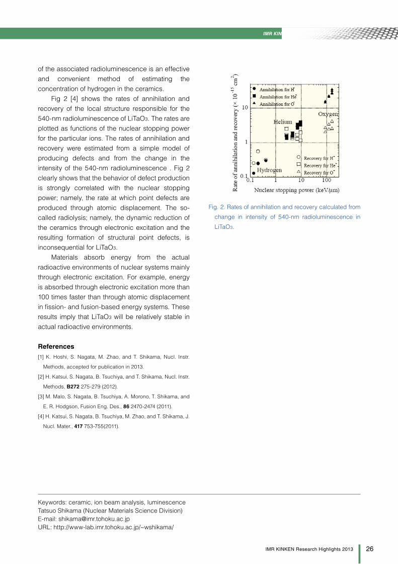
IMR KINKEN Research Highlights 2013
Energy-related Materials
26IMR KINKEN Research Highlights 2013
IMR KINKEN Research Highlights 2013
of the associated radioluminescence is an effective and convenient method of estimating the concentration of hydrogen in the ceramics.
Fig 2 [4] shows the rates of annihilation and recovery of the local structure responsible for the 540-nm radioluminescence of LiTaO3. The rates are plotted as functions of the nuclear stopping power for the particular ions. The rates of annihilation and recovery were estimated from a simple model of producing defects and from the change in the intensity of the 540-nm radioluminescence . Fig 2 clearly shows that the behavior of defect production is strongly correlated with the nuclear stopping power; namely, the rate at which point defects are produced through atomic displacement. The so-called radiolysis; namely, the dynamic reduction of the ceramics through electronic excitation and the resulting formation of structural point defects, is inconsequential for LiTaO3.
Materials absorb energy from the actual radioactive environments of nuclear systems mainly through electronic excitation. For example, energy is absorbed through electronic excitation more than 100 times faster than through atomic displacement in fission- and fusion-based energy systems. These results imply that LiTaO3 will be relatively stable in actual radioactive environments.
References
[1] K. Hoshi, S. Nagata, M. Zhao, and T. Shikama, Nucl. Instr.
Methods, accepted for publication in 2013.
[2] H. Katsui, S. Nagata, B. Tsuchiya, and T. Shikama, Nucl. Instr.
Methods, B272 275-279 (2012).
[3] M. Malo, S. Nagata, B. Tsuchiya, A. Morono, T. Shikama, and
E. R. Hodgson, Fusion Eng. Des., 86 2470-2474 (2011).
[4] H. Katsui, S. Nagata, B. Tsuchiya, M. Zhao, and T. Shikama, J.
Nucl. Mater., 417 753-755(2011).
Keywords: ceramic, ion beam analysis, luminescenceTatsuo Shikama (Nuclear Materials Science Division)E-mail: [email protected]: http://www-lab.imr.tohoku.ac.jp/~wshikama/
Fig. 2. Rates of annihilation and recovery calculated from
change in intensity of 540-nm radioluminescence in
LiTaO3.

27 IMR KINKEN Research Highlights 2013
Energy-related Materials
IMR KINKEN Research Highlights 2013
The mechanical degradations of nuclear materials strongly depend on the environments of the materials. The alloys used in light-water reactors are affected by irradiation-induced defects and possibly by simultaneous interaction with coolant water (i.e., corrosion). Further, the properties of the alloys used in fusion reactors deteriorate through the accumulation of both defects and helium. Therefore, it is indispensable to understand the microstructural evolutions and resulting mechanical degradations of the materials under the environmental conditions the materials are located. We employ irradiation techniques such as ion accelerators and high voltage electron microscopes, conducted with microscopic, spectroscopic, and mechanical property measurements to reveal irradiation effects in Fe- and Zr- based alloys in order to determine how the radiation affected the alloys. The results of this research are further extended to materials development.
This report describes irradiation-induced phenomena in iron- based alloys.
(1) Irradiation Embrittlement of Reactor Pressure Vessel (RPV) Steels [1]
As one of the projects for the Enhancement, Management and Maintenance of Aging Nuclear Power Plants mandated by the Nuclear and Industrial Safety Agency (NISA), the irradiation- induced embrittlement of RPV steels was investigated using ion beams, nano- hardness tester and electrical conductivity measurements to elucidate fundamental insights into the radiation damage, as well as the embrittlement in the heat-affected zones (HAZs) in weld joints.
Ion beam irradiation is one of the methods capable for the precise correlation of the degree of radiation damage and resulting hardening. The correlation of irradiation hardening and embrittlement is also desired in terms of microstructure. Bainitic phase is a typical RPV steel (A533B) consisting of colonial distribution of carbides embedded in a ferrite matrix. The mechanical properties of the steel and their susceptibility to irradiation were systematically investigated. The nano- hardness of
the A533B steel irradiated with 2.8 MeV Fe2+ ions at 563 K is shown in Fig. 1 Irradiation-induced hardening is evident, and the hardening is consistently greater in the carbide colony regions than in the ferrite matrix. This finding suggests that the volume which contains carbide colonies is more susceptible to irradiation hardening than the ferrite matrix. The degree of radiation hardening was roughly proportional to the square root of the dose in both regions up to 1 displacement per atom (dpa). Significant hardening in the carbide colony regions can be explained by the effect of the carbide/ferrite interface, which works as sink for point defects. The effect of the radiation dose rate on hardening was also observed. The degree of hardening increased with decreasing dose rate.
The electrical resistivity was measured to determine how the solute atoms diffused throughout the alloy matrix. The solute atoms trapped vacancies, reducing the rate of vacancy annihilation and enhancing solute atom diffusion.
In order to obtain the technical basis to judge the necessity of the in-reactor surveillance specimens from the HAZ of weld joints, the neutron
Effects of Displacive Radiations in Fe and its AlloysTo develop materials for advanced fission and fusion reactors, we investigated irradiation effects in iron and iron-based alloys with special emphasis on modeling the microstructural evolutions and resulting changes in the mechanical properties of the alloys. A533B alloy irradiated with ions at does up to 1 displacement per atom (dpa) revealed irradiation-induced hardening, and microstructural observation and electrical conductivity measurements were used to determine the mechanism by which the hardening had occurred. Molecular dynamics calculation was applied to investigate the behavior of defect clusters. The solute-defect interaction affected the migration of the defect clusters, giving the characteristic length of the one-dimensional migration.
Fig. 1. Nano-hardness of A533B steel irradiated with 2.8 MeV Fe2+ ions. Dose rate was set at 10-5 and 10-4 dpa/s. Irradiation temperature was set at 563 K.

IMR KINKEN Research Highlights 2013
Energy-related Materials
28IMR KINKEN Research Highlights 2013
IMR KINKEN Research Highlights 2013
irradiation was performed. The fracture toughness of the irradiated specimens and the probabilistic fracture mechanics analysis revealed that each HAZ was susceptible to irradiation embrittlement. The results suggest that fragmented micro-cracks were formed at the fine grained HAZ (FGHAZ).
(2) Modeling glide motion of interstitial clusters in random alloys [2, 3]
Clusters of up to a few tens of interstitial atoms directly formed through large collision cascades under high-energy neutron irradiation. In a recent study of developing materials for future nuclear power applications, the nature and behavior of small interstitial clusters were found to be practically important because small irradiation-induced interstitial clusters and precipitates serve as obstacles to dislocation motion and are responsible for irradiation-hardening, and because small interstitial clusters are glissile at a low activation energy along the direction of the Burgers vector. This type of gliding is called “one-dimensional (1D) migration,” and it affects the evolution of defect structures.
Fluctuation in the microscopic distribution of solute atoms serves as a barrier to the 1D migration of interstitial clusters in random alloys. To better understand and model 1D migration in dilute and concentrated alloys, we studied how the energy of formation of the gliding interstitial clusters fluctuated for various alloys. We developed an analytical model in which the total energy for the interaction between an interstitial cluster and individual solute atoms was a superposition of the potential for the interaction between the cluster and individual solute atoms. We then examined how the total interaction energy of a gliding cluster fluctuated. The average amplitude of the fluctuation was directly proportional to the square root of both the solute concentration and the cluster radius. Although the distance separating the local peaks in the fluctuation was virtually independent of the solute concentration and the cluster radius, it was only dependent on the range of the interaction potential. We developed a model for another fluctuation in the interaction energy because of solute-solute interaction, which is effective at solute concentrations higher than a few percent.
The models were used to interpret the results of the molecular statics simulations in which the energy
for the interaction between interstitial clusters in dilute and concentrated Fe-Cu alloys on the one hand and randomly distributed solute atoms on the other hand fluctuated under systematically varied conditions. The typical height of the local energy peaks in the spectra for concentrated alloys exceeded a few electron volts even though the energy for the individual solute-defect interaction was around 0.1eV. The distance between the local peaks was up to 4 nm. We proposed that the distance was responsible for the short-range 1D migration observed for the various alloys used in the electron irradiation experiments [3]. The amplitude of the fluctuation is attributable to the solute-defect interaction, and gives the characteristic length of 1D migration in alloys.
References[1] H. Abe , K. Onizawa, J. Katsuyama, K. Murakami, Y. Nagai, T.
Toyama, T. Iwai, T. Iwata, Y. Katano, S. Tamura, and N. Sekimura,
IAEA-CN-194, 072 (2012).
[2] Y. Satoh, H. Abe, and T. Matsunaga, Philos. Mag. 93, 1652
(2013).
[3] T. Hamaoka, Y. Satoh, and H. Matsui, J. Nucl. Mater. 433, 180
(2013).
Keywords: radiation effects, electron microscopy, mechanical propertiesHiroaki Abe and Yuhki Satoh (Nuclear Materials Engineering Division)E-mail: [email protected]: http://www-lab.imr.tohoku.ac.jp/~abeken/
Fig. 2. Schematic of present model describing interaction between an interstitial cluster and solute atoms in random binary alloys.

29 IMR KINKEN Research Highlights 2013
Energy-related Materials
IMR KINKEN Research Highlights 2013
Three-dimensional open-cell nanoporous metals have attracted considerable attention for their excellent functional properties including high catalytic activity, sensing capabilities, and surface-enhanced Raman scattering. The properties of nanoporous metals differ significantly from those of their dense, bulky counterparts. Such nanoporous metals have conventionally been prepared by dealloying nanoalloys with aqueous solutions. Dealloying is when the less-noble components in an alloy are etched away and selectively dissolved and the remaining noble components such as Au, Pt, Pd etc. self-organize into a three-dimensional nanoporous structure. The formation of a nanoporous structure is highly desirable not only in noble metals but also in less-noble metals used for various functional applications including energy-harvesting
devices because less-noble metals are abundant and inexpensive. However, metal oxides usually form instead of nanoporous metals during conventional dealloying because of the low stability of the less-noble metals. To overcome this limitation, we have recently used a metallic melt instead of an aqueous solution to develop method of dealloying that increases the yield of nanoporous metals [1-3]. Selective dissolution originates from the interactions among the atoms in metallic melts; therefore, dealloying in metallic melts can even be used to prepare nanoporous less-noble metals. We used dealloying in a metallic melt to prepare a nanoporous Fe-based alloy.
Fig. 1a–c show the scanning electron microscopy (SEM) image and energy dispersive X-ray (EDX) mappings for the cross-section of the as-rolled Fe30Ni70 precursor. The cross-section shows a featureless contrast, and the Fe and Ni elemental mappings show no fluctuations in concentration. These findings are consistent with the formation of a uniform solid solution. The microstructure drastically changed into a fine bicontinuous composite structure, as shown in Fig. 1d, after the precursor was immersed into a Mg melt at 1023 K for 1800 s. The elemental mappings for Fe and Mg shown in Figs. 1e–f reveal that the composite is composed of Fe (bright region) and Mg (dark region). From the equilibrium phase diagrams, the Ni-Mg system is miscible while the Fe-Mg system is immiscible. From the enthalpy of mixing, the interaction between Fe and Mg is repulsive while that between Ni and Mg is attractive. These atomic interactions induced the selective dissolution of Ni from the Fe30Ni70 precursor into the Mg melt, and enabled the remaining Fe atoms to spontaneously form a unique interconnected structure.
Porous Fe-based alloys were formed by removing the Mg phase from the composites. Fig 2a–d show the SEM micrographs of the porous Fe-based alloys prepared by immersing Fe30Ni70, (Fe0.8Cr0.2)30Ni70, and (Fe0.2Cr0.8)30Ni70 into the Mg
Three-dimensional Open-cell Nanoporous Iron-based Alloys
Three-dimensional open-cell nanoporous Fe-Cr alloys were prepared by dealloying Fe-Cr-Ni solid-solution precursors in a metallic Mg melt. Ni was selectively dissolved into Mg, and the remaining Fe and Cr formed a bicontinuous nanostructure when the precursors were immersed into the melt. The size of pores and ligaments were well-tuned by varying the dealloying time and temperature.
Fig. 1 (a) SEM micrograph and elemental mappings for (b)
Fe and (c) Ni for cross-section of as-rolled Fe30Ni70
precursor. (d) SEM micrograph and elemental mappings
for (e) Fe and (f) Mg for cross-section of Fe30Ni70
immersed into Mg melt at 1023 K for 1800 s.

IMR KINKEN Research Highlights 2013
Energy-related Materials
30IMR KINKEN Research Highlights 2013
IMR KINKEN Research Highlights 2013
melt at 1023 K for 10 min. As shown in Fig. 2a, the homogeneous bicontinuous structure spans the entire sample in both the transverse and longitudinal directions. The chemical compositions for these porous samples are Fe99.8Ni0.2, Fe79.0Cr20.5Ni0.5, and Fe19.4Cr80.2Ni0.4 (at.%). Almost no Ni remained in any of the dealloyed porous samples, and the Fe/Cr ratios for the dealloyed porous samples were consistent with those for the precursors. The size of the pores changed depending on the dealloying temperature and immersion time; i.e., lower temperatures and shorter immersion times resulted in structures containing finer pores. The time dependence of pore and ligament size followed a power law whose component was nearly 4, suggesting that surface diffusion plays an important role in forming nanoporous structures. Therefore, the underlying mechanism for forming the porous structure through dealloying in a metallic melt is the same as that for forming the porous structure through dealloying in an aqueous solution.
The preparation of nanoporous less-noble Fe-based alloys whose porous structures are tunable is a significant breakthrough for the cost-efficient development of highly functional materials.
References[1] T. Wada, K. Yubuta, A. Inoue, and H. Kato, Mater. Lett. 65,
1076 (2011).
[2] T. Wada, A. D. Setyawan, K. Yubuta, and H. Kato, Scripta
Mater. 65, 532 (2011).
[3] T. Wada, H. Kato, Scripta Mater. 68, 723 (2013).
Keywords: foam, porosity, microstructureHidemi Kato (Non-Equilibrium Materials Laboratory Division)E-mail: [email protected]: http://www.nem.imr.tohoku.ac.jp/
Fig. 2 SEM micrographs for surface of porous samples
prepared by immersing (a, b) Fe30Ni70, (c)
(Fe0.8Cr0.2)30Ni70, and (d) (Fe0.2Cr0.8)30Ni70 precursors
immersed into Mg melt at 1023 K for 600 s and by
subsequently removing Mg. Chemical compositions
analyzed using SEM-EDX are labeled on each
micrograph.

31 IMR KINKEN Research Highlights 2013
Energy-related Materials
IMR KINKEN Research Highlights 2013
Hydrogen is expected to be an alternative clean energy carrier for mobile applications. The development of efficient hydrogen-storage technologies is thus a very important issue. There are several candidates for storing hydrogen, such as compressed gaseous and liquid hydrogen and hydrides. Hydrides store hydrogen as hydrogen atoms in a crystal structure and have higher volumetric densities than compressed gaseous and liquid hydrogen. For this reason, many studies have previously been reported on using hydrides as hydrogen storage materials.
There are several types of hydrides in which complex hydrides are ionically bonded to metal
cations and hydrido-complex anions. For instance, lithium aluminum hydride, LiAlH4, is composed of a Li+ cation and four [AlH4]- complex anions with covalent Al-H bonds (i.e., the so-called “alanates”). They show much higher gravimetric hydrogen densities (e.g., LiAlH4: 10.6 mass%) than conventional metal hydrides (e.g., LaNi5H6: 1.4 mass%) [1]. In addition to the studies on using complex hydrides for hydrogen storage materials, some studies show lithium- and sodium-ion conduction in complex hydrides containing [BH4]-, [NH2]-, or [AlH6]3- complex anions [2, 3]. Therefore, complex hydrides are interesting energy-related materials as not only hydrogen storage materials but also lithium and sodium-ionic conductors.
Aluminum-based complex hydridesSince the discovery of reversible hydrogen
release (i.e., dehydrogenation) and uptake (i.e., rehydrogenation) in Ti-doped NaAlH4 under moderate conditions (i.e., temperature: <473 K and hydrogen gas pressure: <10 MPa) [4], aluminum-based complex hydrides containing aluminum hydrido-complex anions (i.e., alanates) have been intensively studied [1]. Their decomposition reactions are described by
3NaAlH4 ↔ Na3AlH6 + 2Al + 3H2 (g)↑ ↔ 3NaH + 3Al + 9/2H2 (g)↑.
Such reversible reactions were recently achieved for isomorphic LiAlH4 [5], which has a higher gravimetric hydrogen density and a lower dehydrogenation temperature than NaAlH4. The crystal structure of LiAlH4 is illustrated in Fig 1.
Many researchers have attempted to experimentally and theoretically elucidate the microscopic mechanism for the dehydrogenation of alanates on the basis of precursory phenomena. However, the mechanism has not yet been well-understood.
Changes in Lattice Dynamics of Aluminum-based Complex Hydrides during Hydrogen releaseAluminum-based complex hydrides (e.g., LiAlH4, NaAlH4) are candidate materials for hydrogen-storage technologies because of their high gravimetric and volumetric hydrogen densities and their reversible hydrogen release (dehydrogenation) and uptake (rehydrogenation) reactions. However, the atomic-level mechanism for dehydrogenation has not yet been well-understood. We used inelastic neutron scattering to study the changes in the lattice dynamics of LiAlH4 with increasing temperature. The librational modes of the [AlH4]- anion showed not only obvious broadening but also obvious softening in the range 250–300 K, which is interestingly much lower than the dehydrogenation temperature for LiAlH4 (>426 K). The results suggest that dehydrogenation originates from low-temperature bulk instability/anharmonicity because of the weakened bonds between the complex anions and their surroundings.
Fig. 1 Crystal structure of LiAlH4 (top) and local structure of [AlH4]- surrounded by Li+ (bottom). Li, Al, and H atoms and [AlH4]- are displayed as red, yellow, and blue circles and cyan tetrahedra, respectively.
LiAlH4 takes monoclinic structure with a = 4.8254 Å, b = 7.8040 Å, c = 7.8968 Å, and β = 112.268º in P21/c space group (No. 14) [6].

IMR KINKEN Research Highlights 2013
Energy-related Materials
32IMR KINKEN Research Highlights 2013
IMR KINKEN Research Highlights 2013
Lattice dynamics of aluminum-based complex hydrides [7]
Inelastic neutron scattering (INS), on the other hand, has often been used to investigate atomic motions (i.e., lattice dynamics) in which the intensity is proportional to inelastic neutron-scattering cross-sections. Interestingly, hydrogen has a large inelastic neutron-scattering cross-section (82.02 barns; 1 barn = 1.0 × 10⁻²⁴ cm2), which is approximately 10 times larger than those for most other elements. In addition, although INS has no selection rules, studies on Raman and infrared spectroscopies use them. For those reasons, numerous lattice dynamics of hydrides have been elucidated using INS [8].
We therefore used INS spectroscopy to investigate the temperature dependence of the lattice dynamics of LiAlH4 below the dehydrogenation temperature (426 K) in order to understand the microscopic origins of the dehydrogenation reaction [7]. We particularly focused on the translational and librational modes (i.e., the external [AlH4]- motions) rather than the Al-H bending and stretching modes (i.e., the internal [AlH4]- motions) because the external [AlH4]- motions are expected to show more temperature dependence than the internal ones from previously reported Raman spectroscopy results for NaAlH4 [9]. The INS spectra for LiAlH4 measured from 20 to 300 K and the characteristic schematic figures of the translational and librational modes of [AlH4]- are shown in Fig. 2.
The overall spectra start to broaden with increasing temperature in the range 100–150 K. In addition, the librational modes of the [AlH4]- anion, exhibit not only broadening but also softening in the range 250–300 K. This phenomenon occurs at temperatures surprisingly much lower than the dehydrogenation temperature. This result suggests that the dehydrogenation stems from low-temperature bulk lattice instability/anharmonicity, in particular, because of the weakening of the binding between the [AlH4]- anions and their surroundings.
Further research is needed to understand this phenomenon from the combined perspectives of the local structure and the present dynamic study. This article was produced according to ref. 7.
References[1] S. Orimo, Y. Nakamori, J. R. Eliseo, A. Züttel, and C. M. Jensen,
Chem. Rev. 107, 4111 (2007).
[2] H. Oguchi, M. Matsuo, S. Kuromoto, H. Kuwano, and S. Orimo,
J. Appl. Phys. 111, 036102 (2012).
[3] M. Matsuo, S. Kuromoto, T. Sato, H. Oguchi, H. Maekawa, H.
Takamura, and S. Orimo, Appl. Phys. Lett. 100, 203904
(2012).
[4] B. Bogdanović and M. Schwickardi, J. Alloys Compd. 253-
254, 1 (1997).
[5] X. Liu, H. W. Langmi, S. D. Beattie, F. F. Azenwi, G. S. McGrady,
and C. M. Jensen, J. Am. Chem. Soc. 133, 15593 (2011).
[6] B. C. Hauback, Z. Kristallogr. 223, 636 (2008).
[7] K. Tomiyasu, T. Sato, K. Horigane, S. Orimo, and K. Yamada,
Appl. Phys. Lett. 100, 193901 (2012).
[8] T. Sato, A. J. (Timmy) Ramirez-Cuesta, K. Ikeda, S. Orimo, and
K. Yamada, Inorg. Chem. 50, 8007 (2011).
[9] E. H. Majzoub, K. F. McCarty, and V. Ozolinš, Phys. Rev. B 71,
024118 (2005).
Keywords: energy storage, neutron scatteringToyoto Sato and Shin-ichi Orimo (Hydrogen Functional Materials Division)E-mail: [email protected], [email protected]: http://www.hydrogen.imr.tohoku.ac.jp/
Fig. 2 INS spectra for LiAlH4 measured in 20–300-K range and characteristic schematic figures of translational (<400 cm-1) and librational (400–500 cm-1) modes [7].
Pink dotted line in spectra indicates softening above 250 K. Black arrows in schematic figures indicate directions of atomic motions

33 IMR KINKEN Research Highlights 2013
Energy-related Materials
IMR KINKEN Research Highlights 2013
IntroductionsVarious large bulk crystals have been grown
from melts with the Czochralski and Bridgeman methods; these grown crystals are used in many industrial and research fields after forming processes such as cutting from the bulk crystals and polishing of the cut crystals. However, the forming processes after crystal growth greatly affect the manufacturing cost and increase the prices of the final products using the crystal elements.
The micro-pulling-down (μ-PD) method is a crystal growth method that uses a crucible with a die at the bottom. Compared to conventional methods, the μ-PD method has a great advantage in that a shaped single crystal can be grown with a specially shaped crucible [1]. Because of its potential for the near–net shape growth of a single crystal, the μ-PD method is expected to be applied in mass production.
Development of Shaped CrystalsShaped sapphire crystals with various
configurations and multiple shaped sapphire crystals were grown by the μ-PD method using molybdenum crucibles with various shaped dies [2]. All shaped crystals had high transparency and
visible inclusions, and no cracks were observed in the crystals. The crystallinity of each shaped crystal was evaluated by X-ray rocking curves, and all crystals indicated a high crystallinity of less than 100 arcsec.
We developed a novel Pt alloy crucible with a suitable wetting angle for a langasite-type melt. Columnar, plate, and tube-shaped La3Ta0.5Ga5.5O14 (LTG), Ca3NbGa3Si2O14 (CNGS), Ca3TaGa3Si2O14 (CTGS), Sr3NbGa3Si2O14 (SNGS), and Sr3TaGa3Si2O14 (STGS) piezoelectric crystals were grown using Pt alloy crucibles with special-shaped dies [3]-[8]. The shaped langasite-type crystals indicated comparable piezoelectric properties to previously reported results. In addition, a combustion sensor test device using the shaped langasite-type crystal was developed.
After the nuclear accident in Fukushima, the demand for dosimeters has greatly increased. However, previous dosimeters using a semiconductor had low sensitivity to radiation, and those using scintillators with high sensitivity were expensive. Therefore, we developed a growth method for shaped Ce-doped Y3Al5O12 (Ce:YAG) scintillator crystals to decrease the price of dosimeters. Facets of as-grown crystals can be controlled by the crystal orientation of the seed crystal; the facet surfaces had high transparency without polishing. A dosimeter using the shaped Ce:YAG crystals without polishing was developed, and it indicated good sensitivity to radiation.
Recently, a novel Ir alloy with high oxidation resistance was developed and used for a spark plug in an engine. However, the Ir alloy is unworkable, and the thin wire had to be made from the Ir alloy cylinder by scraping. In order to develop a shaping technology for Ir alloy wire with one operation, we developed a ceramic crucible that can be used at 2400 °C without evaporation or breaking, and a shaped Ir alloy wire was grown in it.
Growth of Shaped Crystals and their Application in Device Fabrication
Device size–shaped crystal growth technology has been established using the micro-pulling-down method. Devices using these shaped crystals have started to become commercially available. Shaped sapphire crystals, langasite-type piezoelectric crystals for combustion sensors, scintillator crystals for pocket real-time dosimeters, and Ir-based alloy crystals for spark plugs have been grown in specially shaped crucibles.
Fig. 1 Shaped sapphire crystals grown by μ-PD method.

IMR KINKEN Research Highlights 2013
Energy-related Materials
34IMR KINKEN Research Highlights 2013
IMR KINKEN Research Highlights 2013
References[1] A. Yoshikawa, M. Nikl, G. Boulon, and T. Fukuda, Opt. Mat. 30,
6 (2007).
[2] A. Yoshikawa and V. Chani, MRS Bull. 34, 266 (2009).
[3] Y. Yokota, V. Chani, M. Sato, K Tota, K Onodera, T. Yanagida,
and A. Yoshikawa, J. Cryst. Growth 318, 983 (2011).
[4] Y. Yokota, M. Sato, K. Tota, Y. Futami, T. Yanagida, K. Onodera,
and A. Yoshikawa, Jpn. J. Appl. Phys. 50, 09ND03 (2011).
[5] Y. Yokota, M. Sato, V. Chani, Y. Futami, K. Tota, S. Kurosawa,
K. Onodera, and A. Yoshikawa, Sensors and Actuators A (in
press) doi.org/10.1016/j.sna.2012.10.017.
[6] Y. Yokota, A. Yoshikawa, Y. Futami, M. Sato, K. Tota, K.
Onodera, and T. Yanagida, IEEE Trans Ultrason Ferroelectr
Freq Contr. 59, 1868 (2012) .
[7] Y. Yokota, Y. Futami, M. Sato, K. Tota, K. Onodera, T. Yanagida,
and A. Yoshikawa, IEEE Trans Ultrason Ferroelectr Freq Contr.
59, 1864 (2012).
[8] Y. Yokota, M. Sato, Y. Futami, K. Tota, T. Yanagida, K. Onodera,
A. Yoshikawa, J. Cryst. Growth 352, 147 (2012).
Keywords: crystal growth, piezoelectric, radiation effectsAkira Yoshikawa (Advanced Crystal Engineering Laboratory)E-mail: [email protected]: http://yoshikawa-lab.imr.tohoku.ac.jp/
Fig. 2 Shaped piezoelectric, scintillator and Ir alloy crystals grown by μ-PD method and developed combustion sensor test
device and dosimeter using shaped crystals.

35 IMR KINKEN Research Highlights 2013
Energy-related Materials
IMR KINKEN Research Highlights 2013
1. IntroductionIn recent years, rare earth elements (REEs)
have become recognized as important materials since they are widely utilized in the production of magnets, fluorescent materials, laser crystals, etc. [1]. Since Japan is the largest consumer of REE products, exploration of alternative supply routes is important for resource security.
Coal fly ash contains relatively high concentrations of REEs at several hundred parts per million weight. REEs are known to be soluble in an acidic solvent. In this study, we examined the dissolution behavior of REEs in dilute acidic solvents in order to determine the feasibility of REE recovery using an acid-washing process.
2. Materials and MethodsThree types of coal fly ash specimens were
used: Ash-A, Ash-B, and IRANT EOP. Ash-A and Ash-B were provided by an electrical power company in Soma, Fukushima, in Japan. In order to determine the REE concentrations in Ash-A and Ash-B and verify the accuracy of the measurements obtained by inductively coupled plasma mass spectrometry (ICP-MS), the REE concentrations in the specimens were determined by means of acid
digestion. The equipment for the dissolution test comprised a Pyrex beaker, magnetic stirrer, heater with a stirring magnet, electrodes (to monitor the pH, redox potential, and temperature of the solutions), and laptop computer. ICP-MS measurements were then taken for the solutions against the rhenium internal standard.
3. ResultsFig. 1 displays the dissolution behavior of
lanthanum in a dilute H2SO4 solvent as an example. The dissolution rates increased with the temperature of the H2SO4 solution, and Ash-B had a higher dissolution rate than Ash-A. The other REEs show dissolution behavior quite similar to lanthanum.
4. DiscussionThere seem to be two types of REE speciation
in coal fly ash. Some of the REEs in the original coal tend to volatilize during coal combustion and are then deposited onto the surface of coal fly ash particles [2]. The other type of REE transition is the accompaniment of blown-up ash components from the original coal. In this case, REEs are melted with ash components and distributed into the coal fly ash particles. If their dissolution is assumed to be controlled by interlayer diffusion, the unreacted core model [3] can fit the dissolution rate very well with a variance of greater than 0.87. The intercepts for all of the fitting lines were non-zero. Similar trends were found for the rest of the REEs considered in this study. Therefore, these fitting lines suggest two types of REE occurrence. In the early stages of dissolution, REEs at the surface of the coal fly ash dissolve immediately to result in a drastic increase of (3(1 − f)2/3 − 2f). REEs inside the coal fly ash particles then dissolve gradually, which corresponds to the linearity of the fitting line [4].
Dissolution Behavior of REEs from Coal Fly Ash by Extraction Using Dilute H2SO4 Solvent
In order to clarify the partitioning and dissolution behavior of rare earth elements (REEs) in coal fly ash particles, tests of acid digestion and acid dissolution using ICP-Mass Spectrometry (ICP-MS) were conducted. The REE concentrations followed the Oddo–Harkins rule. The unreacted core model fitting revealed that REEs exist both on the surface of coal fly ash particles and inside them.
Fig. 1 Change in lanthanum dissolution rate over time.

IMR KINKEN Research Highlights 2013
Energy-related Materials
36IMR KINKEN Research Highlights 2013
IMR KINKEN Research Highlights 2013
5. ConclusionLaboratory-scale dissolution experiments were
conducted to determine the REE content in coal fly ash particles and investigate their dissolution behavior in H2SO4 solvents. In the dissolution tests, dissolution rates of REEs increased with the temperature of the H2SO4 solvent. The transition of the REEs was attributed to surface deposition and accompaniment, and the probabilities of both processes could be explained by applying the unreacted core model to the dissolution behavior of REEs from coal fly ash in H2SO4 solvent.
References[1] JOGMEC, “Material Flow of Mineral Resources,” 2010
[2] R. Meij. 39 199 (1994).
[3] S. Yagi and D. Kunii, Chemical Engineering Science, 16, 364
(1961).
[4] S. Kashiwakura, Y. Kumagai, H. Kubo, and K. Wagatsuma.
Open Journal of Physical Chemistry, 3 69 (2013).
Keywords: mass spectroscopy, waste managementKazuaki Wagatsuma, Shigeo Sato, and Shunsuke Kashiwakura (Analytical Science Division)E-mail: [email protected]: http://wagatsuma.imr.tohoku.ac.jp/index.html
Fig. 2 Dissolution rates of REEs in a dilute H2SO4 solvent
fitted by unreacted core model assuming that dissolution
is controlled by interlayer diffusion.

Electronic Materials
37 IMR KINKEN Research Highlights 2013 IMR KINKEN Research Highlights 2013
In 2005, the theoretical prediction of a new class of materials known as topological insulators [1] promised novel physics and the potential for various applications. The key distinction from ordinary insulators lies in the fact that topological insulators support stable gapless boundary modes. Topological insulators owe their unique properties to time-reversal symmetry: if the flow of time is reversed, the material would behave in the same way. One of most striking foundations is that the surface states are protected from any perturbation, which preserves the time-reversal symmetry when the bulk energy gap remains intact. Anderson localization is topologically forbidden on the surface of topological insulators even in the presence of disorders.
On the other hand, magnetic impurities cause an effective mass gap in the Dirac spectrum on the surface. When the Fermi level resides in the surface gap, a quantized anomalous Hall effect is realized. As depicted in Fig. 1 (a), applying an electric field produces a Hall current on the surface of the topological insulator, which generates a magnetic
field, or magnetization in the bulk. This electrically induced magnetization without dissipation is referred to as the topological magnetoelectric (ME) effect [1, 2]. This type of cross-coupling is described by the energy density functional
(1)
where θ=π for a topological insulator and θ=0 for an ordinary insulator.[2] The topological ME effect is not only a useful signature of a topological insulator but has a variety of potential applications. Therefore, the stability of this effect is of central interest to researchers in this community.
We studied the effect of magnetic disorder on the surface of a topological insulator and clarified that randomness unexpectedly enhances the surface quantized anomalous Hall effect that helps realize the topological ME effect [3]. Using scaling analysis, we clarified that all surface states are localized because of magnetic impurities, while the quantized Hall plateau width becomes enlarged
Entangled Electromagnetic and Thermal Responses of Topological Insulators and Superconductors
We studied the nontrivial responses of topological insulators and superconductors to determine their electromagnetic and thermal potentials. Magnetization was generated by application of an electric field, which is known as the topological magnetoelectric (ME) effect. We investigated the stability of the ME effect and clarified its robustness with regard to randomness and a strong magnetic field. We generalized this cross-coupling to the case of thermal response and predicted that the temperature gradient generates orbital angular momentum.
Fig. 1 Illustration of a magnetically doped topological insulator with (a)a cylindrical geometry and (b)a slab geometry.

Electronic Materials
IMR KINKEN Research Highlights 2013
IMR KINKEN Research Highlights 2013
38IMR KINKEN Research Highlights 2013
from the original surface gap to all energy regions. We recently studied the effect of bulk impurities [4] and electron–electron [5] interaction. The topological phase withstands such perturbations to some extent.
By using the quantized Hall surface states, surface magnetization can be controlled through the application of both electric and magnetic fields: to get the energy gain in Eq. (1), all surface spins tend to point out perpendicular to the surface. In the presence of only the magnetic field, on the other hand, all surface spins point in the same direction to the field because of Zeeman coupling.
We recently examined this topological ME effect in a thin-film topological insulator [6]. When the width of the film was not very thin, we found that the ME effect worked even beyond the linear response regime.
Topological superconductors are superconductor analogs of topological insulators [1]. The bulk has a finite superconducting gap, while there are gapless Andreev bound states on the surfaces. Topological superconductors intrigue physicists because they are expected to host exotic particles on the surface known as Majorana fermions that differ fundamentally from any other known particles in the sense that the particles are their own antiparticles [1]. Since Majorana fermions are expected to have applications in quantum computation, detecting and manipulating them are the great challenges in the field.
We predicted the existence of a unique and unexpected signature of topological superconductors: a temperature gradient applied to a topological superconductor generates mechanical rotation, i.e., orbital angular momentum[7].
The magnetoelectric coupling in topological insulators is because electrons moving along the surface of a sample under the influence of an electric field generates a magnetic field or magnetization in the bulk. Similarly, Majorana fermions on the surface
of topological superconductors moving under the influence of a temperature gradient contribute to the orbital angular momentum. Simultaneously, the thermal Hall conductivity, which characterizes the heat transport of Majorana fermions on the surface, is quantized in terms of universal constants and the mean temperature. This feature indicates that the effect should be stable over extrinsic perturbations. We obtained the free energy describing this nontrivial thermomechanical coupling as [7]
(2)
where v is the Fermi velocity and Ω is the angular velocity. The Einstein–de Haas effect reveals the relationship between magnetism and angular momentum of the system and has been used for the study of ferromagnetic materials. We assumed a cylindrical three dimensional (3D) topological superconductor suspended by a thin string and applied a thermal gradient. This induced a surface energy current with angular momentum Lz. By the conservation law of total angular momentum of the material, which can be directly measured in principle, the inverse effect is the generation of thermal polarization induced by rotating the material [7].
References
[1] M. Z. Hasan and C. L. Kane, Rev. Mod. Phys. 82, 3045
(2010).
[2] X.-L. Qi, T. L. Hughes, and S.-C. Zhang, Phys. Rev. B 78,
195424 (2008).
[3] K. Nomura and N. Nagaosa, Phys. Rev. Lett. 106, 166802
(2011).
[4] S. Ryu and K. Nomura, Phys. Rev. B 85, 155138 (2012).
[5] A. Sekine, T. Z. Nakano, Y. Araki, and K. Nomura, Phys. Rev.
B 87, 165142 (2013).
[6] D. Baasanjav, O. A. Tretiakov, and K. Nomura, in preparation.
[7] K. Nomura, S. Ryu, A. Furusaki, and N. Nagaosa, Phys. Rev.
Lett. 108, 026802 (2012).
Keywords: insulator, electrical properties, magnetic propertiesKentaro Nomura (Theory of Solid State Physics Division)E-mail: [email protected]: http://www-lab.imr.tohoku.ac.jp/~nomura/index.html

Electronic Materials
39 IMR KINKEN Research Highlights 2013 IMR KINKEN Research Highlights 2013
A magnetic field is a powerful and precise tuning knob for matter such as magnetic and semiconducting materials. It induces various new states with unexpected magnetic and electronic properties. Photospectroscopy is widely used as one of the most powerful means to investigate the states of materials. However, the combination of these two tools has mostly been limited to magnetic fields of less than 20 T at university laboratories. This is because a superconducting magnet is used in most cases; such magnets are easy to handle, and a continuous magnetic field is supplied, but the maximum field is limited. Resistive water-cooling magnets and pulsed magnets that generate magnetic fields of above 20 T are operational in dedicated high magnetic field laboratories. Pulsed magnets are running in smaller laboratories having specialists for high magnetic fields.
Besides the limited maximum magnetic field, there are some technical difficulties in combining a superconducting magnet with optical spectroscopy experiments. A large stray field has a strong influence on detectors and optical systems driven by motors. The optical pass can be as long as a few meters in 20-T magnets; in many cases, an optical fiber is used in such experiments. This is not compatible with techniques such as wide-band THz time domain spectroscopies, which need a direct optical pass.
Compact bench-top pulsed high magnetic field generators, which were developed by the magnetism division of IMR, are a new breakthrough in this field. The idea is very simple. The energy needed for a pulse magnet is known to scale with both the magnet volume and the square of the magnetic field intensity. When a magnet is reduced in scale, the energy can be reduced, and the power supply can be compacted [1]. Because of the compactness of the magnet, the system can easily be placed on the optical bench of the
spectrometer. Even so, extremely strong magnetic fields of 30 T are easily obtained. The instrument and operational costs are quite small. For example, the full set including a magnet shown in Fig. 1 costs
Bench-Top Pulsed Magnet for Tabletop SpectrometerA bench-top pulsed magnet generator was developed for spectroscopies such as photo luminescence and THz spectroscopy. Magnetic fields of up to 30 T can be generated on a standard optical bench. The compactness of the system is useful for a wide range of magneto-spectroscopy experiments. The system extends the range of high magnetic fields in small laboratories by offering an extremely strong magnetic field of 30 T.
Fig. 1(a) View of bench-top 30 T pulsed magnet installed in Rice University. The magnet is installed inside the tall cryostat (left panel). The capacitor bank is installed close to the optical table (right upper panel). The wave form is recorded by an oscilloscope (right middle panel). A sample is cooled by the micro-spectroscopy cryostat in the center. In this photo, the cryostat has been temporarily removed from the bam axis shown by arrows. An ultrafast laser, lens system, and detector are arranged on the optical bench for normal zero field experiments (bottom panel).

Electronic Materials
IMR KINKEN Research Highlights 2013
IMR KINKEN Research Highlights 2013
40IMR KINKEN Research Highlights 2013
only a few million JPY, and cheap liquid nitrogen is used for magnet cooling instead of expensive liquid helium.
Fig. 1 shows the bench-top spectroscopy setup. The magnet is installed in the compact liquid nitrogen cryostat, and the magnet inner bore is 13 mm in diameter. The distance from the optical window to the magnet center is only 35 mm. The cryostat can be put on the optical bench, and no special probe is needed for 30 T experiments. The power supply stores an energy of 11.2 kJ and charged with 2 kV. The energy required for 30 T is about 9 kJ. The rise time and total pulse width are 2 ms and 10 ms, respectively. By combining this system with a compact cryostat used for micro-spectroscopy, a sample can be cooled down to 5–10 K. The experimental setup in Fig. 1 is at Rice University, Houston. The first results of fluorescence in a semiconductor superstructure have been reported elsewhere [2].
The system is quite versatile in terms of both generating magnetic fields and application to spectroscopies. The 16 kJ system designed for the Photon Science Institute of Manchester University, as shown in Fig. 2, can be upgraded to charging at 4 kV. The system will be used for THz spectroscopies [3].
In summary, the bench-top 30 T pulsed magnet system developed at IMR will extend the frontiers of magneto-spectroscopies and increase the opportunities for new findings in research on magnetic and semiconducting materials.
References[1]Y. Narumi, T. Nakamura, T. Kinoshita, Y. H. Matsuda, and H.
Nojiri, SRN 25, 12 (2012).
[2]H. Nojiri and Z. W. Ouyang, Terahertz Sci. Technol. 5, 1
(2012).
[3]G.Noe II, H. Nojiri, J. Leotin. G. Woods, A. Belyanin and J.
Kono, Proc. of CLEO2013, San Jose, June 9-14, (2013).
Keywords: high magnetic field, spectroscopy, instrumentationHiroyuki Nojiri (Magnetism Division)E-mail:[email protected]: http://www.hfpm.imr.tohoku.ac.jp
Fig. 2 16 kJ capacitor bank exported for the Photon Science Institute at Manchester University using the Material Transfer Agreement protocol of Tohoku University. The dimensions are 760 mm wide × 1000 mm long × 1400 mm high (upper panel). The capacitor, charge-discharge, and high-voltage power supply components are assembled as independent units; thus, a flexible upgrade is possible. The inside view of the charge-discharge unit. The high-voltage terminal is on the right front side. The matching filter is on the left front side (lower panel).

Electronic Materials
41 IMR KINKEN Research Highlights 2013 IMR KINKEN Research Highlights 2013
The ferroelectricity induced by electrons [1], not conventional ionic displacements, is currently being explored in the field of strongly correlated electron systems, which is related to the charge-ordered state of Mott insulators. Molecular dimer Mott insulators are a good candidate for ferroelectricity and are constructed from dimers of organic molecules such as bis(ethylenedithio)tetrathiafulvalene (BEDT-TTF). When each dimer in a crystal possesses a charge carrier, particularly for the half-filled case of a dimer molecular orbital, the electron system often shows a Mott transition for relatively large (onsite) Coulomb interactions U at the dimer site compared to the electron hopping energy t. An important physical insight is that a dimer can be viewed as the primitive constituent in a crystal rather than as a molecule, as shown in Figs. 1(a) and 1(c). In this manner, the understanding of strongly correlated electron systems based on the dimer picture within the Hubbard model has progressed [2].
However, recent reports on the dielectric properties of several dimer Mott insulators [3-5] have implied that the charge degrees of freedom in a dimer survive even in the dimer Mott insulating state [6,7]. If a charge disproportionation occurs in the dimers, electric dipole moments appear as shown in Figs. 1(b) and 1(d). The fluctuation of charges in dimers can be observed in the dielectric properties. This discovery will enable a deeper understanding of organic Mott insulators beyond the successful dimer lattice model.
β′-(BEDT-TTF)2ICl2 is an anisotropic quasi two-dimensional molecular dimer Mott insulator with a one-hole carrier in the dimer of a BEDT-TTF molecule. The molecular dimer forms the square lattice shown in Figs. 1(c) and 1(d). The dimers are aligned along the b axis, arrayed in a column on the bc plane; the layers are stacked along the a* axis (⊥ bc plane) and are well separated by ICl2 anion layers. Dimerization was supported by NMR [8] and calculation of the intradimer transfer integral. The long-range antiferromagnetic order [9] below TN = 22 K, as shown in Fig. 2(c) indicated that this system is located inside the well-defined dimer Mott insulating region with a large U/t value.
Fig. 2(a) shows the temperature dependence of the dielectric constant ε for β′-(BEDT-TTF)2ICl2 in E ||b parallel to the dimer array at each frequency [6]. An anomaly with a strong frequency dependence was discerned at around 80–150 K. With decreasing frequency, the anomaly in the dielectric constant becomes large and forms a peak structure. A similar frequency-dependent dielectric constant was observed for κ-(BEDT-TTF)2Cu2(CN)3 [3], which is typically seen in relaxor ferroelectric materials with randomness and frustration.
The dielectric constant obeys the Curie–Weiss law with a constant term: ε/ε0 = C/(T – TC) + εconst./ε0. Here, ε0, C, and TC are the vacuum permittivity, Curie constant, and Curie temperature, respectively. The Curie constant C was obtained according to the fit to the Curie–Weiss law. The dipole moment parallel to the b axis was estimated to be 0.13ed, where e and d are the electron charge and distance between the BEDT-TTF molecules in a dimer, respectively.
Relaxor Ferroelectricity Induced by Electron Correlation in Molecular Dimer Mott InsulatorThe charge degrees of freedom in the molecular dimer Mott insulator β′-(BEDT-TTF)2ICl2 were investigated. An anomalous peak structure with strong frequency dependence on the temperature dependence of the dielectric constant and corresponding glassy polarizations along the dimer direction were observed. These results suggest that the charge degrees of freedom in dimers fluctuate and survive even in a dimer Mott insulator.
Fig. 1 Schematic crystal structure of κ-(BEDT-TTF)2Cu2(CN)3 in (a) and (b) and β′-(BEDT-TTF)2ICl2 in (c) and (d). The upper two panels represent the dimer lattice model, and the lower two represent the dipole dimer model. The circles in the dimer lattice model are the sites of the dimers where the molecules in the dimers are ignored. The ovals in the dipole dimer model represent the dimers. The circles in the oval are molecules where a dipole moment can emerge if a charge disproportionation occurs.

Electronic Materials
IMR KINKEN Research Highlights 2013
IMR KINKEN Research Highlights 2013
42IMR KINKEN Research Highlights 2013
The inset of Fig. 2(b) shows the fit to the data for E ||b of β′-(BEDT-TTF)2ICl2 to the Vogel–Fulcher (VF) relation for ε: f = f0 exp−EVF/(Tmax − TVF), where f0 , EVF , and Tmax are the representative flipping frequency of electric dipoles, average random energy barrier, and temperature at which ε takes a maximum, respectively. The empirical VF relation accurately represents the frequency dependence of the peak in ε with TVF = 23 K, EVF = 804 K, and f0 = 2.17 × 10⁷ Hz. TVF is very close to the Neel temperature of 22 K. This implies a possible relation between the glassy dielectric behavior and the magnetic property.
Fig. 2(b) shows the electric polarization P with E ||b obtained by pyrocurrent measurements, and (c) shows the temperature dependence of the magnetic susceptibility in a magnetic field with H ||a*, b, and c for β′-(BEDT-TTF)2ICl2. A small but measurable polarization was observed below the temperature of TFE = 62 K, which is nearly identical to the estimated TC = 67 K from the Curie–Weiss behavior. However, the experimentally obtained polarization of 6 nC/cm2 at Epol = 1.2 kV/cm was ~100 times smaller than the expected full polarization using the Curie constant. A fully polarized state has not yet been obtained under poling electric fields of 1.2 k V/cm. Thus, such a polarization indicates the formation of glassy polar domains, which is also consistent with the strong frequency dependence of ε.
The temperature dependence of the magnetic susceptibility shown in Fig. 2 (c) is explained by a two-dimensional Heisenberg model with an antiferromagnetic interaction JAF of 59 K [9]. Around this temperature, the magnetic susceptibility significantly decreased, which indicates a short-range spin correlation in the low-dimensional system. This energy scale is comparable to TFE, which also implies a relation between the glassy nature of the dielectric and antiferromagnetic interaction. Several scenarios based on the spin-charge correlation in the dielectric anomalies have been proposed [3-7].
However, deepening understanding of the charge-spin correlation and the dielectric is a topic for future research.
References[1] S. Ishihara, J. Phys. Soc. Jpn. 79, 011010 (2010).
[2] H. Kino and H. Fukuyama, J. Phys. Soc. Jpn. 64, 2726 (1995),
H. Seo, C. Hotta, and H. Fukuyama, Chem. Rev. 104, 5005
(2004).
[3] M. Abdel-Jawad, I. Terasaki, T. Sasaki, N. Yoneyama, N.
Kobayashi, Y. Uesu, and C. Hotta, Phys. Rev. B 82, 125119
(2010).
[4] P. Lunkenheimer, J. Mueller, S. Krohns, F. Schrettle, A. Loidl,
B. Hartmann, R. Rommel, M. de Souza, C. Hotta, J. A. Schlueter,
and M. Lang, Nat. Mater. 11, 755 (2012).
[5] S. Iguchi, S. Sasaki, N. Yoneyama, H. Taniguchi, T. Nishizaki,
and T. Sasaki, Phys. Rev. B 87, 075107 (2013).
[6] M. Naka and S. Ishihara, J. Phys. Soc. Jpn. 79, 063707
(2010).
[7] C. Hotta, Phys. Rev. B 82, 241104(R) (2010).
[8] K. Miyagawa, K. Kanoda, and A. Kawamoto, Chem. Rev. 104,
5635 (2004).
[9] N. Yoneyama, A. Miyazaki, T. Enoki, and G. Saito, Bull. Chem.
Soc. Jpn. 72, 639 (1999).
Keywords: dielectric properties, electronic material, organicSatoshi Iguchi and Takahiko Sasaki (Low Temperature Condensed State Physics Division)E-mail: [email protected]: http://cond-phys.imr.tohoku.ac.jp/
Fig. 2 Temperature dependence of (a) dielectric constant for frequencies from 20 Hz to 200 kHz in E||b, (b) polarization by pyrocurrent measurements along the b axis for poling electric field of +/-1.2 kV/cm, and (c) magnetic susceptibility in H ||a*, b, and c for β′-(BEDT-TTF)2ICl2. The inset in (b) shows the Vogel-Fulcher plot for the frequency dependent dielectric constant. The vertical dashed lines show the temperatures of TFE = 62 K and TN = 22 K.

Electronic Materials
43 IMR KINKEN Research Highlights 2013 IMR KINKEN Research Highlights 2013
Metal-oxide-semiconductor field-effect transistors (MOSFETs) have supported advances in the contemporary information society. The large-scale integration and performance of these transistors have been developed rapidly. Controlled dopant position and density would gain prominence, as device scales decrease to less than 30 nm. Since the electrical properties of these devices are sensitive to the spatial distribution of dopants in them, an analytical technique for determining the exact location of each dopant is desired.
Atom probe tomography (APT) can be used for determining the three-dimensional (3D) distribution of individual dopants in materials with nearly atomic-scale resolution. In laser-assisted APT, a pulsed laser combined with high standing voltages is applied to a needle-shaped specimen, resulting in the ionization and extraction of the atoms on the apex, also known as field evaporation. The elemental distribution and mass-to-charge-state ratio of each atom are determined using spatially resolved time-of-flight analysis.
The development of sample preparation techniques using a focused ion beam (FIB) equipped with a high-resolution scanning electron microscope (SEM) has greatly improved sampling productivity for site-specific analysis. A combination of sophisticated FIB techniques and APT instruments has enabled us to obtain 3D dopant distribution in device structures (Figs. 1(a) and 1(b)) and contribute to broad areas of research in device physics [1-4].
The characteristic variability in MOSFETs has increased substantially owing to their continuously decreasing feature sizes. In particular, the variability in n-MOSFETs is larger than that in p-MOSFETs. Through statistical analysis using APT, we found that an anomalous redistribution of dopant (boron) occurs in n-MOSFETs owing to ion irradiation during source/drain extension (SDE) formation (Fig. 1(c)) [2]. To clarify the electrical variability, we directly obtained the channel dopant concentration of actual n-MOSFETs whose threshold voltage (VT) widely
ranging from ±4.0σ deviation from the median VT in one million (1024 × 1024) transistors. We attempted to fabricate a needle-shaped specimen (Fig. 2(a)). Fig. 2(b) shows the elemental map of the main dopants (boron, phosphorus, and arsenic), nickel, and oxygen atoms. APT assessments revealed that VT is positively correlated with the channel boron concentration (Fig. 2(c)) [3].
With respect to multi-gate (non-planar) device structures, dopant distribution analysis of finFET, a potential future device structure, was carried out. Fig. 3(b) exhibits the elemental map of a prototype boron-doped fin array, tilted at ~45° [4]. The point is that near-surface dopant distribution in non-planar
Three-Dimensional Elemental Analysis in Semiconductor-Based Actual Devices with Atom Probe TomographyLarge-scale integration and high performance of metal-oxide-semiconductor field-effect transistors have been achieved with continuous shrinkage and the emergence of complicated architectures (from planar-type to multi-gate-type). The electrical properties rely on the element distribution. Hence, there is a growing need for characterizing the elemental distributions in three dimensions (3D). Laser-assisted atom probe tomography (APT) has been attracting attention for visualizing elements in semiconductor materials with atomic-scale resolution. The process of sample preparation using a focused ion beam (FIB) with a high-resolution scanning electron microscope has been improved for site-specific analysis, which has contributed to nanoelectronics-related application studies. Herein, we show dopant distribution in planar-type actual devices for validating the origin of electrical variability. Non-planar transistors can also be characterized using APT.
Fig. 1 (a) Cross-sectional transmission electron microscope (TEM) image of our device structure. (b) 3D elemental map of dopants in 65-nm-node n-MOS device structures. (c) Normal probability plots for n- and p-MOSFETs with/without SDE formation.

Electronic Materials
IMR KINKEN Research Highlights 2013
IMR KINKEN Research Highlights 2013
44IMR KINKEN Research Highlights 2013
devices can be obtained using APT after being filled with amorphous silicon by low-energy silicon beam deposition without a significant temperature rise. Oblique sample preparation is required for obtaining a uniform spatial resolution across the edge regions because the spatial resolution of APT in the lateral direction is lower than that in the depth direction [5]. We found that the boron concentrations in the top and bottom of the sample are higher than that in sidewall. Nevertheless, the amount of boron in the sidewall is higher than the amount of activated boron resulting from thermal annealing.
Thus, the combination of a sample preparation technique and APT enables us to characterize dopant distribution in devices having complicated structures.
References[1] K. Inoue, H. Takamizawa, Y. Shimizu, T. Toyama, F. Yano, A.
Nishida, T. Mogami, K. Kitamoto, T. Miyagi, J. Kato, S. Akahori,
N. Okada, M. Kato, H. Uchida, and Y. Nagai, Appl. Phys.
Express 6, 046502 (2013).
[2] H. Takamizawa, Y. Shimizu, K. Inoue, T. Toyama, N. Okada, M.
Kato, H. Uchida, F. Yano, A. Nishida, T. Mogami, and Y. Nagai,
Appl. Phys. Lett. 99, 133502 (2011).
[3] H. Takamizawa, Y. Shimizu, K. Inoue, T. Toyama, F. Yano, A.
Nishida, T. Mogami, N. Okada, M. Kato, H. Uchida, K. Kitamoto,
T. Miyagi, J. Kato, and Y. Nagai, Appl. Phys. Lett. 100, 253504
(2012).
[4] H. Takamizawa, Y. Shimizu, Y. Nozawa, T. Toyama, H. Morita,
Y. Yabuuchi, M. Ogura, and Y. Nagai, Appl. Phys. Lett. 100,
093502 (2012).
[5] Y. Shimizu, Y. Kawamura, M. Uematsu, M. Tomita, T. Kinno, N.
Okada, M. Kato, H. Uchida, M. Takahashi, H. Ito, H. Ishikawa,
Y. Ohji, H. Takamizawa, Y. Nagai, and K. M. Itoh, J. Appl. Phys.
109, 036102 (2011).
Keywords: atom probe tomography, 3D structure, electronic materialYasuo Shimizu, Koji Inoue, and Yasuyoshi Nagai (Irradiation Effects in Nuclear and Their Related Materials Division)E-mail: [email protected]: http://wani.imr.tohoku.ac.jp/
Fig. 3 (a) Cross-sectional scanning TEM image of silicon fin arrays. Observed region is indicated by broken curve. (b) Elemental map of specimen tilted at ~45°. (c) One-dimensional concentration profiles of oxygen and boron across (i) top, (ii) sidewall, and (iii) bottom interfaces.
Fig. 2 (a) Cross-sectional TEM image of 65-nm-node MOSFET. (b) Elemental map of n-MOSFET (VT = 0.421 V). Nickel, phosphorus, arsenic, oxygen, and boron atoms are shown. Silicon atoms are not shown. (c) Correlation between VT and channel boron concentrations in 25 × 25 × 30 nm3 box just below gate oxide.

Electronic Materials
45 IMR KINKEN Research Highlights 2013 IMR KINKEN Research Highlights 2013
Further progress in InGaN-based light-emitting devices is required for their widespread use. However, overcoming the decrease in the radiative recombination rate due to the quantum-confined Stark effect is a serious challenge in the longer wavelength region, where In concentration and misfit strain increase. To this end, non-polar and semi-polar InGaN growth is an attractive alternative. Furthermore, these surfaces have in-plane anisotropy in atomic structures depending on the direction of the c-axis. The efficiency of In incorporation into an InGaN film grown on a miscut [1010] m-GaN substrate depends on the sign of the off-angle toward the [0001] (Ga-polar) or [0001] (N-polar), as shown in Figs. 1 (a) and (c) [1].
For clarifying the origin of incorporation asymmetry, the c-polarity was precisely determined using anomalousdispersion X-ray diffraction (ADXRD). The crystal structure factor of wurtzite GaN hkh + kl reflection is given as follows:
,
and its kinematic intensity for the same h, k, and |l |is proportional to
,
where fGa and fN are the atomic scattering factors of Ga and N, respectively, and u = 0.376 is the N position’s internal parameter.
When a Cu-K X-ray is used, fGa and fN are practically real. Then, the diffraction intensities of the wurtzite hkh + kl and hkh + k l reflections are identical. However, closely above the K (1s) absorption edge of Ga, the imaginary part of fGa is sufficiently large (anomalous dispersion), and the difference in the intensities of the two reflections is detectable. It was estimated from the crystal structure factor that the intensity of 2021 is larger than that of 202 1, while the intensity of 2022 is smaller than that of 202 2. In addition, it was confirmed that the kinetically and dynamically calculated intensities were nearly identical by measuring the reflections from a 330-μm-thick m-GaN for a skew-symmetric geometry.
Three InGaN films, each approximately 150-nm
thick, were grown at 750 °C by metalorganic vapor phase epitaxy on +5°, 0°, and -5° miscut m-GaN substrates. The conventional 2θ-ω X-ray-diffraction spectra of these films are shown in Figs. 1(a), (b), and (c). Anomalous-dispersion x-ray diffraction measurements were performed at beamline 13XU in SPring-8. The c-polarity of the samples was determined such that agreement between the calculated and measured values was obtained for intensity variation along the 202 2, 202 1, 2021, and 2022 series of reflections. As a result, it was confirmed that the In incorporation efficiency at the positive off-angles, where +c [0001]- direction sticks out of the miscut m-surface (Fig. 2(a)), is higher than that at the negative off-angles (Fig. 2(b)).
Additionally, the anisotropy of the m-plane induces the characteristic elongated-island morphology and phase separation into different In-content regions. Fig 3(a) shows a differential-interference-contrast microscopy image of the islands elongated about 10 μm along the a-axis, observed after the partial strain relaxation of the InGaN film grown on a 0°-off m-plane GaN substrate.
Anisotropic Features of m-Plane InGaN GrowthNitride semiconductors such as InN, GaN, AlN, and their alloys are very promising materials for fabricating low power consumption, high power, high-frequency devices. InGaN-based blue light-emitting diodes (LEDs) and laser diodes (LDs) are already commercially available. New trends in nitride semiconductors in the region of deep ultraviolet, green, and infrared wavelengths will promote energy-saving device applications and creating new energies. Our studies are related to these new technology trends, including applications such as phosphor-free white LEDs, brilliant green LEDs, high-efficiency solar cells, and the use of nitride semiconductor-based LDs in optical fiber communications systems.
Fig. 1 2θ-ω scan spectra of (1010)-symmetric X-ray diffraction using Cu Kα line from InGaN films grown on m-GaN substrate. The numerical values in the figure indicate the miscut angle of the substrate in the +c direction. Thickness of the InGaN films is about 150 nm for (a), (b), and (c), and 300 nm for (d).

Electronic Materials
IMR KINKEN Research Highlights 2013
IMR KINKEN Research Highlights 2013
46IMR KINKEN Research Highlights 2013
The 2θ-ω X-ray diffraction spectrum of this film is shown in Fig. 1(d). In this case, an approximately 300-nm-thick InGaN film was grown under a triethylgallium flow rate that was 3× higher than that for the other three films shown in Fig. 1 for inducing the desired island morphology. The phase separation of two different In concentrations can be inferred from the two InGaN peaks seen in Fig. 1(d).
To clarify the phase-separation mechanism, the microscopic two-dimensional distribution of In concentration in the InGaN film was observed with microbeam X-ray diffraction. The X-ray beam was focused using a zone plate and slits to be 0.2 μm and 0.5 μm in the vertical and horizontal full-width half-maximum, respectively [2]. The In mole fraction, x, was estimated from the peak position in the reciprocal-space map by considering strain relaxation due to misfit dislocations [1,3]. Fig 3(b) shows the real space mapping of x, where the incident position of the microbeam X-ray is scanned in 0.2-μm steps along the c-axis and in 1.0-μm steps along the a-axis by moving the sample. The size and shape of the high-x region near the center of Fig. 3(b) is comparable to that of the [0001]-side slope (dark contrast area) of the elongated islands in Fig. 3(a). Therefore, it is considered that the In incorporation efficiency is high on the [0001] side of the island surface. Lymperakis et al. calculated the Ga adatom diffusion barrier of m-GaN as 0.93 eV in the c-direction and 0.21 eV in the a-direction [4]. These anisotropic diffusion barriers are consistent with the elongated-island morphology along the a-direction. Furthermore, the small diffusion length in the c-direction induces the nucleation of islands on the m-plane terraces, thus increasing the step density along the c-axis. The In incorporation efficiency increases on the resulting slope toward [0001] owing to the nitrogen-terminated step structure on this side (Fig. 2(a)).
In summary, the in-plane c-polarity of m-GaN was determined using ADXRD. The In incorporation efficiency increases when the +c-direction sticks out of the miscut m-surface. In addition, it was found that the In mole fraction is high on the slope toward [0001] of the islands extended along the a-axis. The formation of these islands is induced by the anisotropic features of m-plane growth and is expected to be applicable for fabricating micro-sized structures.
References[1] T. Hanada, T. Shimada, S. Y. Ji, K. Hobo, Y. H. Liu, and T.
Matsuoka, Phys. Stat. Sol. (C), 8, 444 (2011); 9, 1856 (2012).
[2] Y. Imai, S. Kimura, O. Sakata and A. Sakai, X-ray Optics and
Microanalysis: Proc. 20th Intern. Congress AIP CP1221, 30
(2010).
[3] K. Shojiki, T. Hanada, T. Shimada, Y. H. Liu, R. Katayama, and
T. Matsuoka, Jpn. J. Appl. Phys., 51, 04DH01 (2012).
[4] L. Lymperakis and J. Neugebauer, Phys. Rev. B, 79, 241308(R)
(2009).
Keywords: nitride, vapor phase epitaxy (vpe), x-ray diffraction (xrd)Takashi Matsuoka (Physics of Electronic Materials Division)E-mail: [email protected]: http://www.matsuoka-lab.imr.tohoku.ac.jp/
Fig. 2 Atomic structure of miscut m-plane of InGaN, where miscut angle is 5° (a) and -5° (b).
Fig. 3 Differential-interference-contrast- microscopy image (a) and in-plane distribution of In mole fraction (b) of a partly strain relaxed InGaN layer grown on 0°-off m-GaN substrate.

Electronic Materials
47 IMR KINKEN Research Highlights 2013 IMR KINKEN Research Highlights 2013
Spintronic and magnetic storage devices store information using the magnetization directions of magnetic bits. For maintaining its magnetization along a certain direction, a nanometer-sized magnet should possess high magnetic anisotropy energy that can overcome thermal energy. However, high magnetic anisotropy leads to a large external energy for writing information onto a bit, i.e., for switching the magnetization direction. Thus, in a magnet, the high thermal stability of magnetization, namely, high coercive field (Hc), and the low switching field (Hsw) are competing properties, both of which are crucial for the advancement of spintronic and magnetic storage devices. Therefore, we need to find a solution for this dilemma.
An energy-assisted switching method using external microwave power, which is called microwave-assisted magnetization reversal (MAMR) [1], is considered as a promising method for reducing the switching field of a highly coercive magnet. It applies a radio-frequency magnetic field (Hrf) to a magnet for inducing uniform magnetization precession, thus resulting in decreased Hsw. However, MAMR utilizes the ferromagnetic resonance (FMR) mode, and its frequency (fFMR) is of the order of 100 GHz for a highly coercive magnet. This high fFMR is a serious obstacle for practical applications. Thus, another method for reducing Hsw while maintaining high Hc is eagerly desired. The concept of magnetization switching we propose here is based on the use of spin wave modes in a soft magnet for switching the magnetization in a hard magnet [2].
We prepared exchange-coupled bilayer films consisting of a hard magnetic L10-FePt layer and a soft magnetic Permalloy (Fe19Ni81; Py) layer by employing sputtering systems. In this L10-FePt/Py bilayer, the L10-FePt (110) layer was epitaxially grown on a MgO (110) substrate, resulting in a uniaxial easy magnetization axis along the in-plane [001] direction. Py was exchange-coupled with L10-FePt through the interface. The magnetic moments in Py are spatially twisted when the magnetic field (H) is applied in the direction opposite to that of the
magnetic moments in L10-FePt, which is schematically shown in Fig. 1a. [3] The Py layer thickness (tPy) was varied from 40 nm to 120 nm, while the FePt layer thickness was fixed at 10 nm. Fig. 1b shows the FMR spectrum of L10-FePt/Py for tPy = 100 nm. We observed three resonance peaks at the frequencies (f) of 8.0 GHz, 9.5 GHz, and 13.5 GHz, as indicated by the red, blue, and green triangles, respectively. This experimental FMR spectrum is well reproduced by numerical simulation. From the numerical simulation, we found that perpendicular standing spin wave (PSSW) modes with n nodes were excited in the L10-FePt/Py
Low Field Magnetization Switching of Hard Magnetic L10-FePt Triggered by Spin Wave ExcitationRecent rapid progress in spintronic and magnetic storage devices has required nanomagnets to balance competing goals for high coercive field and low switching field. In this study, we experimentally demonstrated extremely low field magnetization switching in a highly coercive L10-FePt using a spin wave excited in a soft magnetic Permalloy (Ni81Fe19; Py), where Py was exchange-coupled to L10-FePt through the interface. Because a significant decrease of one order of magnitude was achieved in the switching field when the spin wave was excited, this spin wave–assisted magnetization switching is a promising technique for for manipulating the magnetization direction with ultralow energy.
H = -700 Oe
H = -700 Oe
Experiment
Simulation
tPy = 100 nm
Re[∆S
11] (
a.u.
)
12840f (GHz)
141062
a
bn = 0
n = 0
n = 2n = 1
n = 2n = 1
H
Py
FePt
Saturated State
H
Py
FePt
Twisted State
Fig. 1 a Magnetic structures in L10-FePt/Py bilayer. The left (right) panel depicts the direction of magnetic moments in the saturated (twisted) state. A magnetic field (H) was applied along the in-plane [001] direction of the MgO (110) substrate, which corresponds to the easy magnetization direction of FePt. b FMR spectra of tPy = 100 nm for experiment (upper panel) and simulation (lower panel) at H = -700 Oe. The triangles indicate the resonant frequencies of the PSSW modes with n = 0 (red), n = 1 (blue), and n = 2 (green).

Electronic Materials
IMR KINKEN Research Highlights 2013
IMR KINKEN Research Highlights 2013
48IMR KINKEN Research Highlights 2013
bilayer.We measured the anisotropic magnetoresistance
(AMR) curves of the microfabricated L10-FePt/Py element to examine magnetization switching under PSSW-mode excitation. Fig. 2a shows the AMR curve for tPy = 100 nm without the application of Hrf. When H was swept from positive to negative (denoted by red circles), the device resistance change (∆R) showed an abrupt decrease at H = -175 Oe, reflecting the formation of a twisted structure of magnetic moments in Py, as shown schematically. R returned to the baseline of ∆R = 0 Ω at H = Hsw = -2050 Oe, where all magnetic moments of the bilayer were switched. Fig. 2b shows the AMR curve under the application of Hrf = 145 Oe with f = 8.0 GHz. This f corresponds to the resonance frequency of the PSSW mode with n = 0. A decrease in Hsw down to - 325 Oe was obtained, indicating that magnetization switching was induced by the PSSW-mode excitation.
We achieved the desired large reduction in Hsw for tPy = 120 nm. Hsw was reduced from 2000 Oe to 250 Oe at f = 7 GHz and Hrf = 134 Oe. This Hsw reduction is significant compared to that achieved by conventional MAMR techniques, and the excitation frequency remained less than 10 GHz, even for switching in the highly coercive L10-FePt. Because we simultaneously achieved the competing goals of high Hc and low Hsw, spin wave-assisted magnetization switching can be a new technology for information writing across a wide range of spintronic and magnetic storage applications.
References[1] J.-G. Zhu, X. Zhu, and Y. Tang, IEEE Trans. Magn., 44, 125
(2008).
[2] T. Seki, K. Utsumiya, Y. Nozaki, H. Imamura, and K. Takanashi,
Nature Commun., doi: 10.1038/ncomms2737 (2013).
[3] K. Utsumiya, T. Seki, and K. Takanashi, J. Appl. Phys., 110,
103911 (2011).
Keywords: spin wave, magnetic properties, spintronicKoki Takanashi (Magnetic Materials Division)E-mail: [email protected]: http://magmatelab.imr.tohoku.ac.jp/
0
-0.05
-0.10
-0.15
-2000 -1000 0 1000 2000H (Oe)
∆R (Ω
)
tPy = 100 nm
Hrf = 0 Oe
Py
FePt
Py
FePt
Hsw
Hsw
-2000 -1000 0 1000 2000H (Oe)
Hrf = 145 Oef = 8 GHz
a
b0
-0.05
-0.10
-0.15∆R
(Ω)
Fig. 2 Device resistance change (∆R) as a function of H for microfabricated L10-FePt/Py element a without applying rf magnetic field (Hrf) and b under the application of Hrf = 145 Oe. The frequency (f) of Hrf was 8.0 GHz, and tPy was 100 nm. ∆R originates from the anisotropic magnetoresistance effect, where the device resistance depends on the relative angle between the directions of electric current flow and magnetic field. The green arrows indicate the bilayer’s switching field (Hsw).

Electronic Materials
49 IMR KINKEN Research Highlights 2013 IMR KINKEN Research Highlights 2013
The development of all-solid-state thin-film lithium-ion batteries is required for reducing battery size, mitigating safety issues associated with them, and fulfilling the power requirements of recent electronic devices such as cellphones, electric vehicles, and energy storages modules. Oxide-based electrolytes and active materials have great advantages because of their chemical stability in air, and the thin-film processing of these materials is necessary for assembling all-solid-state lithium-ion batteries.
Lithium cobaltate (LiCoO2) is widely used as a cathode material in commercially available lithium-ion secondary batteries. In all solid-state batteries, optimization of the solid/solid interface between an electrode and an electrolyte with high intercalation/deintercalation of lithium ions in the cell is an important issue. The lithium ion migrates in two dimensions along a layer of lithium atoms within the layered LiCoO2 structure (Fig. 1(a)). Therefore, the orientation and morphology of the LiCoO2 films
should be controlled for ensuring good transportation of lithium ions at a cathode–electrolyte interface. The development of an electrolyte with high Li-ion conductivity is another important issue. Garnet-type cubic Li7La3Zr2O12 is a promising electrolyte material because of its high lithium conductivity, wide potential window, and chemical stability in air. Solid-state reaction mainly involved in the synthesis of Li7La3Zr2O12, in which precise control over chemical composition and temperatures above 1500 K are required. The film fabrication of these active and electrolyte materials has been studied by employing physical vapor deposition (PVD) techniques such as pulsed laser deposition (PLD) and sputtering. To date, only a few research groups have reported control over oriented texture under low deposition rates, and the fabrication of well-formed Li7La3Zr2O12 films with good crystallinity has not been reported.
Chemical vapor deposition (CVD) allows the preparation of films under high deposition rates, while affording control over their morphology and
Lithium-containing Oxide Film for All-solid-state Lithium-ion Battery by Chemical Vapor DepositionFor the development of all-solid-state thin-film lithium-ion battery, the oriented textures and chemical compositions of the electrolytes and active materials should be controlled precisely for fast transportation of lithium ions. Furthermore, the deposition rate is required to be high for practical processes. Our group has been developing a process for the chemical vapor deposition (CVD) of the oxide-based cathode and electrolyte film. LiCoO2 cathode films with off-c-axis orientation and garnet-type, cubic Li7La3Zr2O12 electrolyte films were successfully fabricated at high deposition rates by metalorganic and laser CVD.
Fig. 1 (a) crystal structure of LiCoO2, (b)–(d) surface morphologies of (003)- and (104)-oriented LiCoO2 films by CVD, and of (101)-oriented LiCoO2 film by laser CVD, (e), (f) crystal structures of tetragonal and cubic Li7La3Zr2O12, (g)–(h) surface morphologies of tetragonal and cubic Li7La3Zr2O12 by CVD.

Electronic Materials
IMR KINKEN Research Highlights 2013
IMR KINKEN Research Highlights 2013
50IMR KINKEN Research Highlights 2013
orientation. We have developed a laser CVD [1,2] process that could be an effective approach to preparing highly oriented LiCoO2 cathode films and Li7La3Zr2O12 electrolyte films under high deposition rates.
Preparation of LiCoO2 and Li7La3Zr2O12 filmsA highly (003)-oriented LiCoO2 film was grown
on polycrystalline Al2O3 substrate at a deposition temperature of 923 K by CVD (Fig. 1(b)) [2]. Hexagonally faceted flat surface reflected c-planes in the rhombohedral LiCoO2 lattice. Rounded platelet grains were grown in the (104)-oriented LiCoO2 at 1123 K (Fig. 1(c)); the platelet facets in these were (003) LiCoO2 planes tilted 55° relative to the (104) planes. Fig.1(c) depicts the LiCoO2 films by laser CVD under laser power of 150 W. This film showed (101)-orientation, and the deposition rate was 30 μm h−1, which is 100 times greater than that reported in the literature.
Fig 1(g) and (h) shows Li7La3Zr2O12 films prepared by CVD. A film comprising tetragonal Li7La3Zr2O12 having polygonal facets was deposited at 1073 K (Fig.1 (g)), while a cubic Li7La3Zr2O12 film with fine granular surface morphology was formed at a relatively high temperature of 1223 K. The deposition rates of the tetragonal and cubic Li7La3Zr2O12 films were higher than 20 μm h−1. In addition to the Li7La3Zr2O12 crystalline film, amorphous Li-La-Zr-O films with smooth morphology were deposited using laser CVD. The deposition rates of these Li7La3Zr2O12 films were more than 100 μm h−1.
Oriented growth of LiCoO2 filmsHetero-epitaxial growth is a powerful method
for fabricating films oriented along a specific plane and direction on single crystals. LiCoO2 films oriented along (104) and (018) were hetero-epitaxially grown on (100) and (110) MgO substrates by CVD [3, 4]. Fig. 1 shows the surface and cross-sectional morphologies of the (104)- and (018)-LiCoO2 epitaxial films. The surface morphology of the (104) LiCoO2 film contained diagonally arrayed rectangular facets (Fig.1 (a)), whereas the (018) LiCoO2 film exhibited a roof-like structure extended unidirectionally (Fig.1 (b)) toward [110] MgO. Twin structures were formed with in-plane relationships of [010] LiCoO2//[010] LiCoO2 and [421] LiCoO2//[010]
LiCoO2 in the (104) LiCoO2 film and with in-plane relationships of [100] LiCoO2//[100] LiCoO2 in the (018) LiCoO2 film, thus reflecting the striations on cross-sectional textures. The deposition rates of the (104)- and (018)-oriented LiCoO2 films were about 10 μm h−1, almost 100 times greater than those reported for LiCoO2 epitaxial films fabricated by pulsed laser deposition.
References[1] T. Goto and T. Kimura, Thin Solid Films, 515, 46 (2006).
[2] H. Katsui, Y. Yamashita, R. Tu and T. Goto, J. Ceram. Soc.
Jpn., 121, 406 (2013).
[3] H. Katsui and T. Goto, Surf. Coat. Technol., 218, 57 (2013).
[4] H. Katsui, Y. Yamashita, and T. Goto, Key Eng. Mater., 508,
300 (2012).
Keywords: chemical vapor deposition (cvd), microstructure, electronic materialTakashi Goto, Hirokazu Katsui and Akihiko Ito (Multi-Functional Materials Science Division)E-mail: [email protected]: http://www.goto.imr.tohoku.ac.jp/
Fig. 2 Oriented textures of LiCoO2 epitaxial films. The left SEM images are the surface and the cross section of the (104)-oriented film, and the right images are those of (018)-oriented film. Schematic illustrations of the twin structures are also included (i)-(iiii).

Electronic Materials
51 IMR KINKEN Research Highlights 2013 IMR KINKEN Research Highlights 2013
URu2Si2 is one of the most attractive actinide compounds in the heavy fermion system. It shows a second-order transition at 17.5 K; this is accompanied by a large jump in specific heat. However, more than 25 years since the discovery of this transition, the order parameter is remains unknown. Thus, this ordered state is called the “hidden order.” Unconventional superconductivity appears at low temperatures (<1.5 K) as well, coexisting with the hidden-order state.
Recently, we clarified the Fermi surface properties of URu2Si2 in the hidden-order state through quantum oscillation measurements under extreme conditions such as at temperatures as low as 30 mK and under magnetic fields as high as 35 T [1].
The Fermi surface is one of the most fundamental physical quantities that characterize the metal. Thus, it is important task for researchers to elucidate Fermi surfaces experimentally. We have developed a high-sensitivity quantum oscillation technique for the de Haas-van Alphen (dHvA) and Shubnikov-de Haas (SdH) effect, according to which the magnetic susceptibility or resistivity oscillates periodically as a function of the inverse of magnetic field.
A high-quality single crystal is essential for these measurements. Using the Czochralski method in a tetra-arc furnace, as shown in Fig.1, we grew ultra-pure single crystals of URu2Si2 with a residual resistivity ratio (RRR) > 500, which is the best possible quality of URu2Si2.
Fig 2 shows the angular dependence of the dHvA/SdH frequencies in the hidden order state of URu2Si2.
With regards to the low carrier numbers of URu2Si2, all detected Fermi surfaces have low volume, and the topology of the main Fermi surfaces
is of the closed-type with a nearly spherical shape. However, the cyclotron effective masses are extremely large, indicating a heavy fermion system. An anomalous split of the main branch, α, is observed in the basal plane in the tetragonal structure, and the split immediately disappears when the field is tilted to the c-axis, implying a fingerprint of the hidden-order state. High-magnetic-field experiments reveal the Fermi surface instabilities with the field-dependent effective mass. Near 30 T, just below the critical field of the hidden-order state, a new Fermi surface with heavy quasi-particles was found. The interplay between the Fermi surface instabilities due to the Zeeman spin-split leading to the so-called Lifshitz transition and the field-dependent characteristic gap energy plays an important role in the collapse of the hidden-order state. Similar Fermi surface reconstructions under high fields have been detected in our thermopower measurements as well [2]. The polarized neutron experiments reveal the redistribution of magnetization below and above the
Unveiled Fermi surfaces in hidden order state of URu2Si2
Actinide compounds are attracting interest in condensed matter physics because of their unique properties. The 5f electrons are intermediate between itinerant and localized electrons, and show strong spin–orbit interaction. URu2Si2 is a well-known uranium-based heavy fermion compound with a “hidden-order” transition, the origin of which remains unknown. Herein, we present our recent results on quantum oscillation measurements under extreme conditions with ultra-clean single crystals of URu2Si2. The properties of Fermi surfaces and their instabilities under strong magnetic fields are clarified, thus providing a clue to the origin of the hidden order state.
Fig. 1 High-quality single-crystal growth of URu2Si2 using
Czochralski method in tetra-arc furnace.

Electronic Materials
IMR KINKEN Research Highlights 2013
IMR KINKEN Research Highlights 2013
52IMR KINKEN Research Highlights 2013
hidden-order transition, implying a fingerprint of rank 5 multipoles [3]. In addition, a key experiment on thermal expansion under uniaxial stress was performed [4].
This work was done in collaboration with members of CEA-Grenoble (Commissariat à l'énergie atomique et aux énergies alternatives), LNCMI (Laboratoire National des Champs Magnétiques Intenses), ILL (Institut Laue-Langevin), and JAEA (Japan Atomic Energy Agency).
References
[1] D. Aoki, G. Knebel, I. Sheikin, E. Hassinger, L. Malone, T.D.
Matsuda, and J. Flouquet: J. Phys. Soc. Jpn., 81, 074715
(2012).
[2] A. Pourret, A. Palacio-Morales, S. Krämer, L. Malone, M.
Nardone, D. Aoki, G. Knebel, and J. Flouquet: J. Phys. Soc.
Jpn., 82, 034706 (2013).
[3] E. Ressouche, R. Ballou, F. Bourdarot, D. Aoki, V. Simonet,
M.T. Fernandez-Diaz, A. Stunault, and J. Flouquet: Phys. Rev.
Lett., 109, 067202 (2012).
[4] S. Kambe, D. Aoki, B. Salce, F. Bourdarot, D. Braithwaite, J.
Flouquet, and J.P. Brison: Phys. Rev. B, 87, 115123 (2013).
Keywords: actinide, Fermi surface, heavy fermionDai Aoki (Radiochemistry of Metals Division)E-mail: [email protected]: http://actinide.imr.tohoku.ac.jp/
Fig. 2 Angular dependence of dHvA/SdH frequencies in
hidden-order state of URu2Si2. The frequency is
proportional to the extremal cross-sectional areas of the
Fermi surfaces [1].

Electronic Materials
53 IMR KINKEN Research Highlights 2013 IMR KINKEN Research Highlights 2013
The physics of low-dimension quantum antiferromagnets (AF) is fascinating because non-trivial behaviors emerge at low temperatures. The spin-ladder system is a characteristic system that bridges a one-dimensional (1D) spin chain and a two-dimensional (2D) CuO2 layer. A two-leg spin-ladder system is indeed realized with the copper oxide families SrCuO3 [1] and Sr14−x(La,Ca)xCu24O41 [2]. Because superconductivity emerges in the latter system [3], the nature of antiferromagnetic (AF) spin correlation in a spin-ladder system has been investigated in connection with the mechanism of high-Tc superconductivity [4]. However, the quite large nearest-neighbor AF exchange interaction (J ≈ 2000 K) of these compounds prevents observation of the entire spin excitation spectrum [5]. No experimental evidence of two-triplon (coupled triplets on the lungs of ladder) continuum excitation, which is similar to two-spinon continuum excitation in one-dimensional quantum magnets [6], has been detected thus far. To make progress on this issue, we have started an experimental as well as a theoretical study on BiCu2PO6, a new model system, in which the S = 1/2 quantum spins of Cu2+ ions constitute two-leg spin ladders with relatively smaller J (~100 K) [7]. Recently, we grew a high-quality large single BiCu2PO6 crystal (Fig. 1). This progress has enabled us to elucidate the full excitation spectrum of the spin-ladder system through neutron scattering measurements.
Sample preparation and characterizationA single crystal of BiCu2PO with a diameter of 8
mm and length of 100 mm was grown using the floating-zone method. The phase purity and sample mosaic of the grown crystal were confirmed through powder X-ray measurements and the X-ray back Laue method (Fig. 1), respectively. Our sample shows a spin-gap behavior in magnetic susceptibility. Two 35-mm-long samples were co-aligned for the inelastic neutron scattering measurement. To study the overall spin excitation spectrum of BiCu2PO6, in which S = 1/2 quantum spins from Cu2+ ions form a two-leg spin-ladder, we performed the first high-
energy neutron scattering measurement at the chopper spectrometer 4SEASONS [7] installed at J-PARC
Magnetic excitation spectrum in BiCu2PO6
As shown in Fig. 2, the magnetic excitation of BiCu2PO6 was successfully observed in wide momentum and energy spaces. The excitation along the crystallographic b-axis shows clear dispersion with the energy band between 2 meV and 28 meV, while that along c-axis and a-axis (not shown) is non-dispersive. Therefore, the spin correlation is one-dimensional, which is consistent with the result of the antiferromagnetic two-leg spin-ladder model, and a rung singlet is formed at the ground state. Importantly, the spin gap opens at the incommensurate (0, 1 ± 0.45, 0.75) momentum position along the leg direction. This result suggests the existence of a large next-nearest-neighbor interaction, namely, spin frustration along the leg. Thus, the BiCu2PO6 [8] system was confirmed to be
High-energy Neutron Scattering Study of Spin Excitations in New Frustrated Spin Ladder SystemQuantum spin systems have been studied extensively owing to their exotic ground states and non-trivial phenomena. A spin-ladder system is one of ideal systems for testing a theory that bridges a one-dimensional spin chain and a two-dimensional square lattice. To characterize the ground state and magnetic excitations of the newly found two-leg spin ladder BiCu2PO6, we performed a time-of-flight inelastic neutron scattering measurement on its single crystal. Our result indicates triplon excitation with the minimum energy of 2 meV at the incommensurate momentum position. This indicates the formation of a rang-singlet at the ground state and the existence of strong competing interactions along the ladder.
Fig. 1 Grown single crystal of BiCu2PO6 (upper figure) and the Laue pattern taken for a part of crystal (lower figure).

Electronic Materials
IMR KINKEN Research Highlights 2013
IMR KINKEN Research Highlights 2013
54IMR KINKEN Research Highlights 2013
a frustrated spin-ladder system, which affords a unique opportunity to study the novel nature of quantum spin systems. Furthermore, we investigated the temperature dependence of the entire spin excitation for characterizing the thermal evolution of spin correlation in this frustrated spin-ladder system. It was found that the intensity at 28 meV decreases with increasing temperature, and the peak disappears around 70 K. This temperature is consistent with the temperature at which the magnetic susceptibility shows a broad maximum. Therefore, the thermal evolution of the magnetic branch extending at 28 meV closely correlates with the change in magnetic ground state and the degradation of spin-singlet formation at high temperatures.
References[1] Z. Hiroi et al., J. Solid State Chem., 95, 230 (1991).
[2] E. M. McCarron et al., Mat. Res. Bull., 23, 1355 (1988).
[3] M Uehara et al., J. Phys. Soc. Jpn., 65, 92764 (1996).
[4] E. Dagotto, Phys. Rev. B, 45, 5744 (1992).
[5] S. Notbohm et al., Phys. Rev. Lett., 98, 027403 (2007); R.S.
Eccleston et al., Phys. Lev. Lett., 81, 1702 (1998).
[6] M. Arai et al., Phys. Rev. Lett., 77, 3649 (1996).
[7] M. Nakamura et al., J. Phys. Soc. Jpn., 78, 093002 (2009).
[8] B. Koteswararao et al., Phys. Rev. B, 76, 052402 (2007).
Keywords: neutron scattering, spin dynamics, quantum spin systemMotoki Fujita (Materials Processing and Characterization Division)E-mail:[email protected]: http://www.imr.tohoku.ac.jp/en/org/research/27.html
http://www.yamada-lab.imr.tohoku.ac.jp/jp/index.html
Fig. 3 Excitation spectrum of BiCu2PO6 along leg-direction measured at 45 K (upper figure) and at 125 K (lower figure). The intensity of excitation at ~28 meV decreases at high temperatures, suggesting rung-singlet formation degradation.
Fig. 2 Excitation spectrum of BiCu2PO6 along leg direction at l = 0 (upper left figure), l = 0.75 (upper right figure), and along rung direction at k = 0 (lower left figure) and k = 1 (lower right figure). Clear dispersion was observed along the b-direction with the maximum energy of ~28 meV. The minimum energy of ~1 meV was observed at the (0, 1 ± 0.45, 0.75) incommensurate position, suggesting the existence of frustration between the antiferromagnetic nearest and next-nearest neighbor interactions.

Electronic Materials
55 IMR KINKEN Research Highlights 2013 IMR KINKEN Research Highlights 2013
Ni-Nb-Zr ternary alloys have been known to form an amorphous phase in wide concentration regions [1]. The hydrogen permeability of Ni-Nb-Zr amorphous alloy ribbons was investigated by Yamaura et al., and an excellent permeability value of about 1.59 × 10⁻⁸ mol/m-s-(Pa)1/2 was reported for melt-spun amorphous (Ni0.6Nb0.4)50Zr50 alloy [2,3]. In addition, the mechanical properties of hydrogen-absorbed amorphous alloy ribbons were investigated by Kawashima et al [4]. Recently, peculiar behaviors of the electrical transport properties such as superconductivity, electron avalanche behaviors, and Coulomb-blockade oscillations of hydrogen-absorbed [(Ni0.6Nb0.4)1-
x/100Zrx/100] (30 < x < 50) amorphous alloy ribbons were elucidated by Fukuhara et al. [5,6]. They pointed out that the localization effect of hydrogen in outside and inside spaces of the distorted icosahedral Zr5Ni5Nb3 clusters plays important roles in their various electrical transport properties. In other words, the state of hydrogen absorption is thought to be sensitive to the difference in the local structure of the glassy state [3]. Therefore, a systematic study of the effects of hydrogen absorption on the electrical transport properties of the Ni-Nb-Zr amorphous alloy is important for clarifying the mechanisms underlying such peculiar behaviors.
We made amorphous alloy ribbons of Ni36Nb24Zr40, and controlled the amount of the absorbed hydrogen by changing the current density of electrochemical charging. The amorphous alloy ribbons were fabricated by the single roller melt-spinning technique, where the surface velocity of the copper wheel was about 50 m/s. The thickness and width of the fabricated ribbon were about 25 μm and 1 mm, respectively. Hydrogen-absorbed specimens were prepared by electrochemical charging in 0.5 M H2SO4 + 1.4 g/L thiourea (H2NCSNH2) at room temperature with a current density of about 10–120 A/m2 for 2 h. The amount of absorbed hydrogen was measured using the inert gas carrier melting-thermal conductivity method several times under each condition. Thermal analyses were performed with a differential scanning
calorimetry under a heating rate of 0.33 K/s. Phase state was identified using x-ray diffraction with Cu-Κα radiation. The electrical resistivity was measured using a conventional four-probe method in the 6–300 K temperature range with cooling and heating rates of about 0.017 K/s.
Hydrogen absorption effects on electrical resistivity
Fig. 1 shows mass concentration of the hydrogen absorbed by the electrochemical method as a function of current density. Here, the charging time was fixed to 2 h. The amount of absorbed hydrogen in the ribbon specimens was found to increase with increasing current density and to have a tendency to saturate. The maximum value of hydrogen absorption was thought to be limited to a maximum of 0.25 mass% (15 at.%), because the specimens turn very brittle if they are charged with the higher current density of 120 A/m2.
Fig. 2 indicates the x-ray diffraction patterns of a Ni36Nb24Zr40 melt-spun ribbon and specimens charged electrochemically for 2 h under current densities of about 40 and 70 A/m2. The amounts of absorbed hydrogen in these specimens were found
Electrical Transport Properties of Ni-Nb-Zr-H Amorphous Alloy RibbonsElectrical resistivity measurements were carried out for investigating the effects of hydrogen absorption on the electrical transport properties of Ni36Nb24Zr40 amorphous alloy ribbon. The amount of hydrogen absorbed can be controlled by changing the current density of electrochemical charging. The electrical resistivity showed negative temperature dependence, and absolute value of the temperature coefficient of resistivity, TCR, increased as the amount of hydrogen absorbed increased. The negative enhancement of TCR could have originated from an increase in the residual resistivity owing to the induced hydrogen and vacancy.
Fig. 1 Mass concentration of absorbed hydrogen as a function of the current density in the electrochemical charging of Ni36Nb24Zr40 amorphous alloy ribbons. The dashed curve is a visual guide.

Electronic Materials
IMR KINKEN Research Highlights 2013
IMR KINKEN Research Highlights 2013
56IMR KINKEN Research Highlights 2013
to be about 9.2 and 14.7 at.%, respectively. The x-ray diffraction patterns show typical halo-type patterns, indicating an amorphous structure. In Fig. 2, it can be seen that the main peak around 40° shifts to a slightly smaller angle with increasing hydrogen absorption, thus indicating volume expansion.
Fig. 3 shows the temperature dependence of normalized electrical resistivity, ρ/ρ300K, for y = 0.0, 2.0, 3.3, 9.2, and 14.7 in (Ni0.36Nb0.24Zr0.40)100-yHy. All resistivity exhibits negative temperature dependence, according to the Baym-Meisel-Cote theory based on the Boltzmann transport equation for amorphous alloys with non-periodic crystal structure, as follows [7]:
(1)
where ρ0 is the residual resistivity, exp[-2W(T)] is the Debye-Waller factor, ρph is the phonon term, Λ is the mean free path, and q is the wave vector. For the amorphous and quasi-crystals with non-periodic structures, Λ is small, and, consequently, the second term in Eq. (1) becomes negligible. Therefore, the electrical resistivity is governed by the temperature dependence of the Debye-Waller factor and not by the electron-phonon scattering. In such a case, the electrical resistivity shows T2-dependence in the low-temperature range and T-linear dependence close to room temperature [8,9]. As shown in Fig. 3,
absolute value of temperature coefficient of resistivity, TCR, increases with increasing absorbed hydrogen, y, clearly indicating the effect of hydrogen absorption on electrical resistivity. With regards the origins of this effect, there are many possibilities, e.g., the change in the mean free path associated to with volume expansion, change in the Debye temperature and electronic state, and the existence of scattering related to absorbed hydrogen. Clarifying this mechanism is the next objective of our study.
References[1] H. Kimura, A. Inoue, S. Yamaura, K. Sasamori, M. Nishida, Y.
Shinpo, and H. Okouchi, Mater. Trans., 44, 1167 (2003).
[2] S. Yamaura, Y. Shimpo, H. Okouchi, M. Nishida, O. Kajita, H.
Kimura, and A. Inoue, Mater. Trans., 44, 1885 (2003).
[3] S. Yamaura, M. Sakurai, M. Hasegawa, K. Wakoh, Y. Shimpo,
M. Nishida, H. Kimura, E. Matsubara, and A. Inoue, Acta Mater.,
53, 3703 (2005).
[4] A. Kawahima, S. Yamaura, N. Ohtsu, H. Kimura, and A. Inoue,
Mater. Trans., 6, 1523 (2006).
[5] M. Fukuhara, A. Kawashima, S. Yamaura, and A. Inoue: Appl.
Phys. Lett., 90, 203111 (2007).
[6] M. Fukuhara, H. Yoshida, K. Koyama, A. Inoue, and Y. Miura,
J. Appl. Phys., 107, 033703 (2010).
[7] L.V. Meisel and P.J. Cote, Phys. Rev. B, 16, 2978 (1977), ibid.
17, 4652 (1978).
[8] U. Mizutani, Prog. Mat. Sci., 28, 97 (1983).
[9] U. Mizutani, Phys. Stat. Sol. (b), 176, 9 (1993).
Keywords: amorphous, electrical resistivityRie Y. Umetsu (Advanced Materials Development and Integration Novel Structured Metallic and Inorganic Materials)E-mail: [email protected]: http://amdi-pro.imr.tohoku.ac.jp/en/index.html
Fig. 2 X-ray diffraction patterns of Ni36Nb24Zr40 melt-spun amorphous alloy ribbon and hydrogen-absorbed specimens.
Fig. 3 Temperature dependence of normalized electrical resistivity, ρ/ρ300K, for (Ni0.36Nb0.24Zr0.40)100-yHy with y = 0.0, 2.0, 3.3, 9.2 and 14.7.

Research Centers
57 IMR KINKEN Research Highlights 2013 IMR KINKEN Research Highlights 2013
Neutron irradiation using material-testing reactors is common in research on the effects of irradiation on materials. For a more precise understanding of irradiation dose dependency, the maintenance of identical irradiation conditions, i.e., irradiation rate (neutron flux), neutron spectrum, and irradiation temperature, are necessary for different doses. We have started to develop new irradiation rig for providing such series irradiation to collaborators.
Materials irradiation at the Oarai center has been performed using the BR2 reactor of SCK∙CEN, Belgium Nuclear Research Center, after the suspension of JMTR in 2006. A new irradiation rig system, LIfting Basket in the Experimental Rig for BR2 Thimble tube sYstem or “LIBERTY,” is being developed under the framework for collaboration between IMR and SCK∙CEN. LIBERTY’s irradiation specifications are approximately the same as those of JMTR’s rig system in terms of maintaining samples with references under identical conditions of neutron flux and temperature [1].
The new rig system has been improved for fulfilling the specifications and incorporating the following three features. 1) Individual needles can be lifted independently above the reactor core level when the specified fluence is reached, while the other needles remain in the neutron flux. 2) Individual needle can be instrumented separately. Therefore, electrical heating wires and thermo-couples can be installed into the needles for controlling specimen temperature during irradiation. 3) Relatively large specimens such as CT specimens (10 × 10 mm²) can be tested.
The concept underlying LIBERTY is schematically shown in Fig. 1 (a); LIBERTY consists of one shroud tube containing up to five needles with samples inside. Initially all needles are inserted at the bottom position of the shroud, which is in the reactor’s core region. When the desired irradiation dose is achieved, the needle is lifted from the bottom to the top of the shroud. Each needle can be lifted
individually, thus allowing for five different doses. In each needle, we can install holders with samples, thermocouples, and electric heating elements (heating wires). A cross-sectional view of LIBERTY’s core region is shown in Fig. 1 (b); it is worth noting that it is made of the stainless steel shroud tube, of the five larger needles and of the center tube containing the gamma thermometer. The cooling water first flows downward around the needles through the shroud tube, turns upward, and flows between the outer and inner walls of the shroud tube. The rig itself is reusable, and it does not need to be sent to the hot cell for needle loading and unloading; these operations can be performed in the water pool. LIBERTY is now being developed, as shown in Fig. 1 (c), and will be available in FY2013 for collaborative studies.
It is now widely recognized that actinides
Recent Facility Progress at Oarai Center for Material Irradiation Testing and Actinide Materials Science
International Research Center for Nuclear Materials Science (Oarai Center)
Facilities of the Oarai Center are open to experimental studies that involve the use of nuclear reactors and α-emitters materials such as actinides. Recent facility progress is described as follows. A new irradiation rig system that provides several different neutron doses under the same irradiation conditions such as neutron-flux and irradiation-temperature is being developed. The old tetra-arc furnace with a glass bell jar has been renewed for growing high-quality single crystals of uranium and thorium compounds. Low-temperature measurements of nuclear magnetic resonance and Mössbauer spectroscopy, as well as those of electrical resistivity have been achieved by installing a helium-free refrigerator.
Fig. 1 (a) Concept of “lifting-needle irradiation,” (b) cross section of core region, and (c) photograph of LIBERTY prototype.

Research Centers
IMR KINKEN Research Highlights 2013
IMR KINKEN Research Highlights 2013
58IMR KINKEN Research Highlights 2013
represent a unique part of the periodic table of elements. Many interesting physical and chemical properties of actinide materials in the solid and liquid states are derived from the special nature and characteristics of their open shell of 5f electrons. Both sample preparation for high quality, advanced microscopic probe measurement such as dHvA, and NMR and Mössbauer spectroscopies are very important for elucidating the intrinsic role of 5f electrons.
The aging tetra-arc furnace with defects in both ultimate base vacuum and stability of electrode currents was being used for limited sample preparation of polycrystalline intermetallics and lanthanide-based alloys. A new tetra-arc furnace with a Czochralski puller on top of the stainless chamber was installed in the Actinide Laboratory in 2012 to grow high quality single crystals (see Fig.2). High base vacuum after 1 h of evacuation (5 × 10⁻⁶ Torr) and agitation of the titanium getter by the fifth electrode prevent oxidation of the active melting button. Each arc current can be controlled precisely from 3 to 20 A for several hours for growing a cylindrical sample of the single crystal that has a typical diameter of 3–4 mm and is few-millimeters-long. This machine allows for the melting and pulling of the uranium- and thorium-based systems with low vapor pressures and rather high melting temperatures.
Low-temperature physical properties were being measured by conventional helium-type cryostats at the Oarai center. A cryogen-free superconducting magnet with a bore size of 100 mm, homogeneity less than 0.01 %, and maximum field of 6 T (JASTEC JMTD-6T100HH) has been installed for NMR spectroscopy. Another closed-cycle refrigerator for sample cooling from 4.5 K to room temperature (JANIS SHI-950) has been arranged for the superconducting magnet. We can perform not only NMR spectroscopy but also measure electrical resistivity with this cryostat. The high-temperature system with the electric furnace and the very-low-temperature system using ADR in this magnet station are under construction.
Mössbauer spectroscopic measurements at low temperatures are possible using the closed-cycle refrigerator with beryllium windows (Taiyo Nissan corp., Model-331). Temperatures of the Mössbauer source and absorber (sample) are controlled individually for enhancing recoil-less
nuclear resonance, even those of the high-energy γ-rays associated with 237Np and 197Au Mössbauer effects. Conventional Mössbauer measurements of 57Fe and 151Eu nuclides have been also performed using this cryostat. Mössbauer spectra reflect the source conditions, especially those of the 241Am source for the 237Np Mössbauer effect, where alpha decay and strong recoil-less by high-energy γ-rays damages the atomic arrangement of the source matrix. A fine splitting spectrum resulting from the hyperfine field could not been obtained using the old 241Am metal source [2]. We prepared the Pd-10%(Pu,Am) and Pd-5%Am alloys following a coupled reduction process starting with a mixture of Pd and dioxides in He-4%H2 atmosphere at 950 °C. It was demonstrated that the Pd-Am alloy is an ideal source for 237Np Mössbauer spectroscopy owing to its narrow half width and oxidation resistance.
References[1] A. Kuramoto, T. Toyama, T. Takeuchi, Y. Nagai, M. Hasegawa,
T. Yoshiie, Y. Nishiyama, J. Nucl. Mater., 425, 65 – 70 (2012).
[2] Y. Homma, M. Nakada, A. Nakamura, S. Nasu, D. Aoki, H.
Sakai, S. Ikeda, E. Yamamoto, Y. Haga, Y. Onuki, Y. Shiokawa,
Hyperfine Interact., 168, 1 175-1179 (2006).
Tatsuo Shikama (International Research Center for Nuclear Materials Science (Oarai Center))E-mail: [email protected]: http://www.imr-oarai.jp/
Fig. 2 Photograph of tetra-arc furnace.

Research Centers
59 IMR KINKEN Research Highlights 2013 IMR KINKEN Research Highlights 2013
In April 2013, the center was reorganized and renamed as "Cooperative Research and Development Center for Advanced Materials" for making a fresh start in promoting research, principally, on advanced materials. The underlying philosophy of research in the center is to find and establish the fundamental principles and technology for synthesizing and industrializing highly and multi-functional next-generation materials through collaborative research.
Recently, the density functional theory (DFT) simulation has been found to be an effective approach for explaining the mechanism of adsorption on various metal and metal oxide catalyst surfaces. An iron catalyst is commonly used in the Fischer-Tropsch synthesis for fuel production from a gaseous mixture of CO and H2. The feed gas, however, also contains H2S, which can shorten the active life of the Fe catalyst. We have investigated the influence of Na and K on the properties of the CO and H2S molecules adsorbed on a Fe(100) surface [1]. It has been found that the presence of Na and K atoms on the Fe(100) surface promotes the adsorption of CO molecules and hinders the adsorption of H2S molecules, and, in particular, the potassium additive
has been found to induce the largest variations in adsorption energies (Fig. 1(a)). Through examinations of the local density of states and charge analysis, we have shown that electrostatic interactions between the alkali atoms and the molecules are mainly responsible for this enhancement effect (Fig. 1(b)). With the aim of developing a novel absorbent for effective CO2 sequestration, DFT calculations have been employed for studying the adsorption process of CO2 on a CaO (001) surface (Fig. 1(c)). The effect of adding other alkaline earth metal oxides to CaO on the adsorption energy of CO2 has been analyzed (Fig. 1(d)). The structural deformation of the CaO surface due to the formation of a compound or solid solution would result in variations in the adsorption energy, and in the case of CaO/BeO, carbon dioxide capture during adsorption is improved significantly [2].
The handling of glass-forming molten alloys is a very important issue in both basic and applied research on noncrystalline materials. In our center, we proposed the following press release: (i) “Development of Compact Automatic Arc-Furnace” [3] and (ii) “Development of New Atomization Process using High-Velocity Air Fuel Flame” [4]. First, good reproducibility of cast amorphous alloy would be achieved using the automatic fabrication system with the optimized alloying process. The developed compact automatic arc furnace is mainly composed of three components: weighing, alloying, and casting. Because an amorphous material has a featureless structure without a second phase, grain boundaries, and so on, the prealloying process is an important for achieving sufficient master alloy homogeneity by avoiding the formation of unexpected high-melting-point intermetallic compounds. Full use of the automatic arc-furnace could lead to meaningful progress in the advanced quality control of cast amorphous alloys. Second, to produce fine amorphous alloy powder, we investigated high-temperature atomization using a high-velocity air fuel (kerosene) flame (HVAF) (see Fig. 2(a)) because the diameter of atomized powder particles is related to the surface tension and viscosity of the molten alloy. At high temperatures,
Recent Progress in Development of Advanced MaterialsCooperative Research and Development Center for Advanced Materials
(Formerly Advanced Research center of Metallic Glasses)
The center has a critical role to play in the investigation and development of new materials with important functional properties; these materials range from metallic compounds to oxides and from amorphous structures to bulk single crystals. Researchers/students can collaborate with the various research divisions of the center and use its experimental facilities under the inter-university research program.
Fig. 1 (a) Adsorption energies of CO molecule on Fe(001) and alkali/Fe(100) surfaces; (b) Charge density of CO/K/Fe(001) at preferred site; (c) Selected surface model and most stable configuration of CO2 on CaO(001) surface; (d) Density of states and side view of excess (red) and depletion (blue) charges of CO2 on Ca1-xBexO (001) surface (at x=0.02).

Research Centers
IMR KINKEN Research Highlights 2013
IMR KINKEN Research Highlights 2013
60IMR KINKEN Research Highlights 2013
the molten alloy possesses both the attributes. In contrast, conventionally, water or gas is used as the working fluid for powdering in atomization. Because the temperature of the HVAF is approximately 1873 K, a suitable cooling system should be developed for obtaining dry, quenched atomized powder. As shown in Fig. 2(b), we successfully obtained a fine amorphous powder of Fe73.2Cr2.2Si11.1B10.8C2.7 alloy.
Rare-earth aluminoborides REAlB4 with layered structures have attracted considerable attention from researchers. Fig. 3 shows a lattice image and an electron diffraction pattern of an α-TmAlB4 single crystal synthesized under very rapid cooling (> 200 K/h) [5]. All diffraction spots can be indexed as belonging to the α-type phase without additional spots and diffuse streaks, which suggest no structural modulations. The magnetic susceptibility χ of α-TmAlB4 along the c-axis under different fields is shown in Fig. 4(a). Peaks of χ can be observed under lower-magnitude fields, indicating antiferromagnetic (AF) transitions. A sharp λ-like peak of specific heat, C, is observed at around 5.5 K in Fig. 4(b). The behavior of this peak is different compared with the C of slow-cooled (5–50 K/h) α-TmAlB4 containing building defects. The present result shows how the large peak structure in the specific heat curve of the high quality sample can be destroyed by the presence of a small amount of building defects.
The center will continue to promote the development of advanced materials based on fundamental and industrial research using cutting-edge technology.
References[1] M. H. Mahyuddin, R. V. Belosludov, M. Khazaei, H. Mizuseki,
Y. Kawazoe, J. Chem. Phys. C, 115, 23893 (2011). (with Cover
page)
[2] K. Sasaki, K. Wakuta, N. Tokuda, R. V. Belosludov, S. Ueda, Y.
Kawazoe, T. Ariyama, ISIJ International, 52, 1233 (2012).
[3] http://www.tohoku.ac.jp/japanese/2012/11/press20121105-01.
html
[4] http://www.tohoku.ac.jp/english/2013/01/press20130125-01.
html
[5] T. Mori, I. Kuzmych-Ianchuk, K. Yubuta, T. Shishido, S. Okada,
K. Kudou, Y. Grin, J. Appl. Phys., 111, 07E127 (2012).
Akihiro Makino (Cooperative Research and Development Center for Advanced Materials)E-mail: [email protected]: http://www.crdam.imr.tohoku.ac.jp/
Fig. 2 (a) View of HVAF atomization and (b) SEM image of atomized Fe-based amorphous powder.
Fig. 4 Temperature dependence of (a) magnetic susceptibility χ and (b) specific heat, C, of α-TmAlB4.
Fig. 3 Lattice image and electron diffraction pattern of α-TmAlB4 crystal taken along c-axis.

Research Centers
61 IMR KINKEN Research Highlights 2013 IMR KINKEN Research Highlights 2013
The High Field Laboratory for Superconducting Materials (HFLSM) has concentrated on the key research fields of “High field magnet technology,” “Materials science in high fields,” and “Basic research under multiple extreme conditions” as cooperative research in the Institute for Materials Research, Tohoku University. The HFLSM has demonstrated some high field superconducting magnets such as a 30 T hybrid magnet, a 20 T cryogen-free superconducting magnet [1], and a 28 T cryogen-free hybrid magnet [2].
As the next project in the construction of high field facilities in Japan, our group is planning to develop a wide-bore 20 T superconducting magnet with a 400 mm room-temperature bore for a 47 T hybrid magnet [3, 4], a 25 T cryogen-free superconducting magnet, and a 30 T superconducting magnet. Three types of superconducting wires [NbTi, Nb3Sn, and REBa2Cu3O7 (RE : Y or rare-earth elemtnt)] will be used for the three large magnets, and we have been planning to use Nb3Sn Rutherford cables.
We carried out a performance test of a single-layer test coil with five turns using a CuNb-reinforced Nb3Sn (CuNb/Nb3Sn) Rutherford flat cable (Fig. 1). Fig. 2 shows the transport current properties of CuNb/Nb3Sn Rutherford coil. The wide-bore coil with a 270 mm outer diameter was examined in transport currents up to 1500 A at 8 T and 4.2 K. Strain gauges attached to stainless steel tape that was co-wound around the Rutherford flat cable for reinforcement exhibited a strain of 0.25%. These results suggest that we can use the CuNb/Nb3Sn Rutherford cable under such a large electromagnetic force.
We also developed a new fabrication process for the CuNb-reinforcing stabilizer for Nb3Sn wires. One of the serious problems for Nb3Sn wires is that their superconducting properties deteriorate because of the applied strain [5] when a large electromagnetic force is applied in a high field superconducting magnet. In-situ CuNb-reinforced Nb3Sn superconducting wires have been developed to enable the wire to withstand such a large electromagnetic force [6].
Because a large-scale superconducting
magnet has a significant amount of stored magnetic energy, we developed a CuNb-reinforced stabilizer with high electrical conductivity to ensure the cryogenic stability of the large-bore superconducting magnet. Unfortunately, in-situ CuNb has a relatively low electrical conductivity because of the very low
High-strength Nb3Sn Rutherford Cable for47 T Hybrid Magnet
High Field Laboratory for Superconducting Materials
Our group, the High Field Laboratory for Superconducting Materials, is planning to develop a 25 T cryogen-free superconducting magnet, a 47 T hybrid magnet, and a 30 T superconducting magnet. We have been investigating the superconducting wire and cables needed for development of these magnets.
Fig. 1 Photograph of the CuNb-reinforced Nb3Sn Rutherford coil. The single-layer test coil composed of a five-turn Rutherford flat cable was made with sixteen 0.8 mm diameter CuNb/Nb3Sn strands. Stainless steel SUS316L tape was co-wound in order to provide reinforcement against a large electromagnetic force.
Fig. 2 Transport current properties of CuNb/Nb3Sn Rutherford coil at 8 T and 4.2 K. The Rutherford coil was examined in transport currents up to 1500 A.

Research Centers
IMR KINKEN Research Highlights 2013
IMR KINKEN Research Highlights 2013
62IMR KINKEN Research Highlights 2013
solubility of Nb in pure Cu.In order to improve the solubility of Nb in pure
Cu and thus increase the electrical conductivity, we developed a new Nb-rod process in order to fabricate the CuNb-reinforcing stabilizer [7]. Fig. 3 shows the cross section of the Nb-rod-processed CuNb/Nb3Sn wire. The wire is 0.8 mm in diameter.
The superconducting property of the CuNb/Nb3Sn wire under tensile stress at 4.2 K and 14.5 T is shown in Fig. 4. The Nb-rod-processed CuNb/Nb3Sn wire had a maximum critical current Ic at a tensile stress state of 230 MPa, whereas the peak of the Ic stress curve for the in-situ-processed wire appeared at 210 MPa. Therefore, the tensile stress dependence of Ic was improved using the Nb-rod-processed CuNb instead of the in-situ-processed CuNb as a reinforcement material.
References[1] S. Hanai, T. Tsuchihashi, Y. Minemoto, S. Ioka, K. Watanabe,
S. Awaji, H. Oguro, Abstract of CSSJ Conference, 87, 148
(2013). (in Japanese)
[2] K. Watanabe, G. Nishijima, S. Awaji, K. Takahashi, K. Koyama,
N. Kobayashi, M. Ishizuka, T. Itou, T. Tsurudome, J. Sakuraba,
IEEE Trans. Appl. Supercond., 16, 934 (2006).
[3] K. Watanabe, S. Awaji, H. Oguro, K. Takahashi, K. Minegishi,
T. Suwa, Y. Sasaki, T. Kiyoshi, T. Asano, S. Hanai, H. Tsubouchi,
I. Inoue, IEEE Trans. Appl. Supercond., 22, 4300804 (2012).
[4] K. Watanabe, S. Awaji, Y. Hou, H. Oguro, T. Kiyoshi, H.
Kumakura, S. Hanai, H. Tsubouchi, M. Sugimoto, I. Inoue, IEEE
Trans. Appl. Supercond., 23, 4300304, (2013).
[5] J. W. Ekin, Cryogenics, 20, 611 (1980).
[6] H. Sakamoto, S. Endoh, Y. Nagasu, K. Wada, A. Kimura, S.
Meguro, S. Awaji, K. Watanabe, M. Motokawa, IEEE Trans.
Appl. Supercond., 12, 1067 (2002).
[7] H. Oguro, S. Awaji, K. Watanabe, M. Sugimoto, H. Tsubouchi,
J. Supercond. Nov. Magn., 26, 2099 (2012).
Hidetoshi Oguro (High Field Laboratory for Superconducting Materials)E-mail: [email protected]: http://www.hflsm.imr.tohoku.ac.jp
Fig. 3 Cross-sectional view of the 0.8-mm-diameter Nb-rod-processed CuNb/Nb3Sn superconducting wire. The Cu-20vol%Nb-reinforcing stabilizer was placed between copper outside layer and the Nb3Sn superconducting layer.
Fig. 4 Applied tensile strain dependence of the critical current density for the Nb-rod-processed CuNb/Nb3Sn wire and the in-situ-processed CuNb/Nb3Sn wire at 4.2 K and 14.5 T. The Nb-rod-processed CuNb/Nb3Sn has the maximum Ic at a tensile stress state of 230 MPa, whereas the peak of the Ic stress curve for the in-situ-processed wire appears at 210 MPa.

Research Centers
63 IMR KINKEN Research Highlights 2013 IMR KINKEN Research Highlights 2013
Kansai Center was established in Osaka as a special unit within the Institute for Materials Research (IMR), Tohoku University in April 2011 based on an agreement with Osaka Prefecture Government. The Center is sponsored by the government (Ministry of Education, Culture, Sports, Science and Technology) and took over the Osaka Center, who carried out its mission from 2006 to 2011. The mission of the Osaka Center was to support small and medium enterprises in the Osaka area. The area covered by the Kansai Center expanded from the Osaka area to the whole Kansai area. The Center has three missions. First, to solve technical problems that industries have struggled to resolve. Solving such problems is occasionally accomplished through collaboration across universities, research institutions, fields, and institutional boundaries. Some of these activities have developed in collaborative partnerships with industry. Second, the Center introduces academic output to industries, with the aim of applying such output to society. Currently, about 50 enterprises have contracted to engage in joint research on projects of mutual interest, and the Center has vibrant patenting/licensing activities with 23 new invention disclosures. Third, the Center helps educate next-generation materials scientists and researchers in universities and enterprises. To this end, we have organized a bimonthly forum named “Monodukuri Kisokoza,” which focuses on special topics regarding materials and processing.
Projects are conducted through wide collaborations between the government, universities, research institutions, and other organizations such as Osaka Bay-area Consortium, Kansai Bureau Economy Trade and Industry, Research Society for Global Materials Crisis, and General Production Company in order to achieve results efficiently. Among them, the Development Center for New Metallic Material in Osaka Prefecture University and the Research Center for Nano-Micro Structure Science and Engineering at the University of Hyogo are close partners in collaborative projects, and Center staff participates in educating students at both universities. We have seven groups at the Center: Environmental Protection and Energy
Conversion Materials, Functional Materials for Future Industries, Analytical Science and Technology, Structural Materials for a Low-Carbon Society, Nanostructure Control for Engineering Materials, Advanced Biomaterials, and Structure Design of Green Metallic Materials. The Center has four venues to cover the Kansai area: the Osaka office at Osaka Prefecture University, the Hyogo office at University of Hyogo, the Sendai office in IMR, and Monodzukuri Business Information Center Osaka (MOBIO) in the Creation Core Higashi-Osaka, a governmental body where sixteen local universities and one college are located to facilitate collaboration with various industries.
Technical inquiries from industries are handled solely by seven professors in Kansai Center, which helps save investigation and solving time. Fig. 1 shows the number of inquiries from industries to Creation Core Higashi-Osaka. It is apparent that Kansai Center occupies the largest portion among the universities and the number of inquiries increases each year. According to the statistics, about 30% of all inquiries are from enterprises located in areas other than Kansai.
Two special “Monodukuri Kisokoza” series have been held so far (Fig. 2). The first was aimed toward learning more about metals in terms of plasticity, corrosion, and characteristic functions, in addition
Scientific Breakthrough toward Creation of New Industrial Materials
Kansai Center for Industrial Materials Research
Industrial Materials Research (IMR) has launched the Kansai Center, a comprehensive Institute-wide effort that pairs IMR’s research groups across the innovation spectrum to solve today’s industrial challenge and transform tomorrow’s global energy problems. The center was established in April 2011 based on an agreement between IMR, Osaka Prefecture Government, and enterprises in the Kansai area sponsored by government, taking over Osaka Center project.
Fig. 1 Fraction of inquiries (2009–2012) from industries at Creation Core Higashi-Osaka, where sixteen local universities and one college are located. The area in red corresponds to Kansai Center.

Research Centers
IMR KINKEN Research Highlights 2013
IMR KINKEN Research Highlights 2013
64IMR KINKEN Research Highlights 2013
to providing background such as the history and production of metals. Each seminar is composed of basic information and its application, lectures presented by academia and engineers, respectively. So far, six seminars focusing on Ti, Cu, Ni, Al, stainless, and Mg have been held. The second series is organized by the young academic staff at the Center in order to foster collaborative research and development with industries. Each topic is determined by considering the industrial needs and their own specialty. Further, Center professors offer lectures on materials design, technical skills, and related fundamentals of materials science to the students in Osaka Prefecture University and Hyogo Prefecture University for the purpose of demonstrating the importance of material science contributing to industrial applications.
The Center has developed various materials and processes under collaboration with industry. One of them is metallic glass bolts fabricated by squeeze casting and cold-thread rolling (Fig. 3). These bolts have 1.3 times the strength of high-strength steel and are 2 times more difficult to loosen than steel. It is expected that these bolds can be used in biometallics or earthquake-resistant parts in structures [1].
In another successful collaboration, bonding technology using spark plasma sintering (SPS) was
applied to fabricate a bimetallic composite of steel and a Cu alloy for mechanical parts in an axial piston pump. Interdiffusion promotion by SPS strengthens the bonding cohesion through transformation in the steel [2]. Further, high-performance analysis equipment in IMR contributes to new materials fabrication. Nano-sized metallic powders expected to be used for electric devices such as electrodes and metal lines tend to aggregate, a characteristic that needs to be suppressed. A systematic study by using TEM contributed to a new method of fabricating nano-sized powders. The trial products resulting from collaborative projects are displayed in various exhibitions or MOBIO in order to appeal the visitors.(Fig. 4).
The Center recently selected a logo (Fig. 5). The Center’s three missions are embodied by three elements in the logo, and the green leaf in the top right corner symbolizes green innovation. This logo was selected from a design yearbook competition of Japanese typography, yearbook 2013.
References[1] S. Yamanaka, K. Amiya, Y. Saotome, A. Inoue, Mater. Trans.
52, 243 (2011).
[2] N. Masahashi, S. Semboshi, K. Watanabe, Y. Higuchi, H.
Yamagata and Y. Ishizaki, J. Mat. Sci., 48, 5801 (2013).
Naoya Masahashi (Kansai Center for Industrial Materials Research)E-mail:[email protected]: http://www.kansaicenter.imr.tohoku.ac.jp/
Fig. 2 Open seminar “Monodukuri Kisokoza” provides up-to-date information on materials and process technologies to engineers and researchers in industry. Fig. 4 Trial products resulting from collaboration with
industries (displayed in Business Encourage Fair 2012 in Osaka).
Fig. 3 Thread-rolled metallic glass bolt (left) and the SEM micrograph of the screw thread of the bolt (right).
Fig. 5 Newly selected Kansai Center logo advocating the three missions of the Center.

Research Centers
65 IMR KINKEN Research Highlights 2013 IMR KINKEN Research Highlights 2013
Silicon steel is one of the most important industry materials used in transformers, motors, and magnetic coils because of its excellent mechanical and magnetic properties. A higher Si content in steel improves effectively the magnetic properties such as smaller hysteresis, higher permeability, and a lower magnetostriction constant, whereas beyond a certain Si concentration, the mechanical properties degrade rapidly. In order to investigate the origin of the effect of Si concentration on the mechanical properties of high-silicon steel, we employed first-principles calculations for dilute Si in a bcc-Fe solid solution. Carbon and other elements present in the silicon steel were omitted from the calculations in order to reduce the complexity of the calculations. Electronic structures were calculated using density functional theory with Projector augmented wave(PAW)-Generalized gradient approximation (GGA) potential [1-4] on supercell models that simulate various Si concentrations.
First, we investigated the ground-state structures of bcc-based Fe–Si in order to get overall information on the stability of the system. The cluster expansion method [5, 6] has been carried out to predict the 0 K ground state structures in the bcc Fe–Si system. Fig 1 shows the enthalpy of formation versus Si concentration for the various predicted structures by using 41 structures and 34 types of clusters, which led to a prediction of five ground-state structures throughout the entire range of Si concentrations. An Fe-rich D03-ordered bcc structure, which is one of the two bcc-based structures present on the Fe-rich side of the Fe–Si system at finite temperatures, was correctly predicted to be stable at 0 K. We also compared the enthalpy of formation of stable binary compounds in the Fe–Si system (Fe2Si, Fe5Si3, α-FeSi2, β-FeSi2) to confirm the validity of the calculations.
Further work focused on the Si-concentration dependence of various mechanical properties in the dilute Si region of the Fe–Si system [7]. The elastic constants of the dilute Si in bcc Fe structures were calculated using the stress-strain method [8] based on electronic-states calculations on the fully
relaxed Si-doped structures. Fig 2(a) shows the calculated elastic properties, including c11, c12, c44, bulk modulus (B), shear modulus (G), and Young’s modulus (E) at different Si concentrations. A steady change in these properties with increasing Si up to 8.3 at% is shown. These properties decreased clearly insert at 10.9 at% and then
First-principles Study on Mechanical Properties of Fe–Si AlloyCenter for Computational Materials Science
Most of the work performed in Computational Materials Science (CMS) has been centered around the subject of functional properties that can be analyzed directly by the electronic structure of the material. While various mechanical properties of alloys, such as strength and ductility, are basically multiscale phenomena, and few attempts have been made to simulate and analyze the deformation behavior of an alloy from first-principles. Introduced below is a challenging attempt in this direction performed by Prof. Chen’s group, in which they predict the ductile–brittle transition of a Fe–Si alloy. Computer simulation of the mechanical properties is believed to become a key area of CMS performed by supercomputers.
Fig. 1 Ground-states diagram of Fe–Si bcc- based structures: Formation enthalpy vs. Si concentration (at%).
Fig. 2 Calculated elastic properties of dilute Si in bcc-Fe. (a) Elastic constants and modulus. (b) Ratio of bulk
modulus and shear modulus as empirical criteria. between ductility and brittleness of alloy.
(a)
(b)

Research Centers
IMR KINKEN Research Highlights 2013
IMR KINKEN Research Highlights 2013
66IMR KINKEN Research Highlights 2013
rebounded to a certain extent as the Si concentration increased further. This trend is well consistent with experimental results [9]. Fig 1(b) further plots the ratio of the bulk modulus B and the shear modulus G with respect to various Si concentrations. According to Puge’s empirical rule [10], a B/G ratio of 1.75 can be taken as the criterion between ductile and brittle for metal. Thus, the decrease in B/G value from 2.0 to 1.5 at 8.3–10.9 at% Si clearly shows a ductile-to-brittle transition. The origin of the Si concentration dependence of the elastic properties is discussed as following in terms of the evolution of electronic structures.
Fig 3 shows the total electronic density-of-states and the partial electronic density-of-states of Si atoms for pure Fe and 5 Si-doped systems. For all Si concentrations from 0 to 8.3 at% Si, the density of states (DOS) distributions were found to share similar characteristics, whereas noticeably different distributions between 8.3 and 10.9 at% Si were found. It can be seen that for minority-spin at 8.3 at% Si, the Fermi level is at the dip of the two peaks, whereas at 10.9 at% Si, the Fermi level falls just at the peak. This increase in minority-spin led to an obvious increase in the total DOS and resulted in a significant drop of magnetic moment as compared to lower Si concentrations. This indicates that the characteristics of bonding between Fe atoms surrounding Si atoms vary, which is thought to be the direct reason for the change in the mechanical properties with increasing Si concentration.
Further analysis on the redistribution of the electronic structures due to the presence of Si atoms revealed a relationship between magnetism and the elastic properties of the system. Combined with the finite temperature behavior, we reached the conclusion that the interplay between magnetism and the D03 ordering effect resulted in the ductile–brittle transition for Si concentrations of about 8.3 at%. This example shows a modern computational materials science approach based on large-scale electronic structure simulations for investigating, explaining, and predicting the fundamental properties of real materials.
References[1] G. Kresse, VASP, Vienna Ab initio Simulation Package, 2004.
<http://www.vasp.at>.
[2] G. Kresse, D. Joubert, Phys. Rev. B, 59, 1758 (1999).
[3] P.E. Blochl, Phys. Rev. B, 50, 17953 (1994).
[4] P. Perdew, K. Burke, M. Ernzerhof, Phys. Rev. Lett. 77, 3865
(1996).
[5] J. M. Sanchez, F. Ducastelle, and D. Gratias, Physica, 128A,
334 (1984).
[6] W. Connolly and A. R. Williams, Phys. Rev. B, 27, 5169
(1983).
[7] A. Saengdeejing, Y. Chen, K. Suzuki, H. Miura, and T. Mohri,
Comp. Mater. Sci., 70, 100-106 (2013).
[8] Y. Le Page and P. Saxe, Phys. Rev. B, 65, 104104 (2002).
[9] A. Machova and S. Kadeckova, Czech. J. Phys. 27, (5), 555-
567 (1977).
[10] S. Pugh, Philos. Mag. Ser. 7, 45, (367), 823–843 (1954).
Tetsuo Mohri (Center for Computational Materials Science)E-mail: [email protected]: http://www-lab.imr.edu/~ccms/Eng/index.php
Fig. 3 (a) Total electronic density of states of Fe-bcc, Si-doped bcc Fe at 2.7, 5.6, 8.3, 10.9, and 12.5 at% Si. (b) Si partial electronic density of states in Si-diamond, Si-doped bcc-Fe at 2.7, 5.6, 8.3, 10.9, and 12.5 at% Si.

Research Centers
67 IMR KINKEN Research Highlights 2013 IMR KINKEN Research Highlights 2013
It has been a great privilege to cooperate with IMR Laboratories since a long time. I have proposed applying our fruitful relationships with Laboratoire de Physico-Chimie des Matériaux Luminescents (LPCML, nowadays ILM at the Université Claude Bernard Lyon 1) and Institute for Materials Research (IMR, Tohoku University) with the natural continuation of the laser materials research program on rare earth (Nd3+/Yb3+)-doped transparent sesquioxide and spinel ceramics/crystals as laser materials with high melting points. I want to express my thanks to Prof. Niinomi, head of IMR, Prof. Nojiri, head of ICC-IMR, Prof. Konno, TEM Lab, Prof. Goto, SPS Ceramics Lab, and Prof. Yoshikawa, Advanced Crystal Engineering Lab.
The project ELyT lab: M12–LASMAT was started in March, 2012, and included Yoshikawa’s and Goto’s teams. Lu2O3 was selected from among sesquioxides for the following reasons: it is an inactive lattice in optics such as Sc2O3 and Y2O3, Lu3+ can easily be substituted by other rare earth cations as dopants, it has the highest thermal conductivity (12.5 W/m/K) and a lower phonon energy (391 cm-1) as compared with YAG (700 cm-
1). We first focused our attention on Lu2O3 ceramics, and then studied Lu2O3 crystals grown by µ-PD using a special crucible. Indeed, Lu2O3 has a high melting point up to 2490 °C, which makes it extremely difficult to grow by conventional crystal growth methods. Such difficulties encourage researchers seek other ways to obtain Lu2O3 as a ceramic laser material.
Research activity on advanced laser materials is indeed increasing with the availability of transparent sintered polycrystalline ceramics, which present some advantages as compared to single crystals in terms of size, mechanical strength, overall production cost, and cost-effectiveness [1]. After the pioneering work of Dr. A. Ikesue [2] at World Lab. Co. Ltd. and Dr. H. Yagi at Konoshima Company [3] on ceramics fabricated by conventional methods, original and promising research is in progress with the synthesis of Nd3+:Lu2O3 ceramics by a nonconventional spark plasma sintering (SPS) technique developed by Prof. T. Goto’s team [4]. The spectroscopic properties
were analyzed at LPCML (UCBLyon1) and will be compared with the rare earth-doped crystals grown by Prof. A. Yoshilawa’s team. Regarding the spatial distribution of rare earth dopants, we have already published results with A. Yoshikawa’s team on the rare earth segregation phenomenon in YAG laser ceramics, especially from TEM analysis associated with an EDX probe in cooperation with Dr. T. Epicier at the Institut National des Sciences Appliquées de Lyon lab [5-8]. We program the same evaluation with Lu2O3 ceramics.
Another area of interest of Nd3+:Lu2O3 single crystals stems from a 2011 report on the laser output of such crystals [9], which points out that specific dual Nd3+ wavelengths lasing at 1076.4 and 1080.5 nm (see Fig.1) are very promising for applications in coherent terahertz (THz) generation by difference frequency and ultrahigh repetition rate pulse by optical beating.
The fabrication, measurement of thermal conductivity, and structural characterization by TEM will be done at IMR, whereas spectroscopic and laser properties will be analyzed and optimized at ILM. Our first analysis of the absorption spectra, emission spectra, and lifetimes of Nd3+ 4F3/2 level under selective wavelengths made at LPCML (Lyon) have been submitted and discussed with the members of this cooperative project.
I also had the opportunity to attend ICC-IMR-ELyT workshop on materials science on November 27, and I was invited to participate in the Materials Science Week 2012 (MSW2012), Summit of Materials Science, November 28–30, 2012. The intense interest in Materials Science Week is to have access to the large program of IMR on materials. My Invited talk was given for the introductory session (I2) and was titled ”Laser materials: From single crystals to polycrystalline ceramics and distribution of rare earth dopants,” which is directly connected to my IMR cooperation [5-8]. The goal of this lecture was to present the evolution of laser materials from doped single crystals to doped ceramics. Another important cooperation between IMR (Prof. T. Konno, Prof. K. Sato), INSA-Lyon (Dr. T. Epicier), and us in UCBLyon1 involved detection of Yb dopants at the
Crystal Growth and Spectroscopic Properties of Laser Single Crystals/Ceramics
International Collaboration Center (ICC-IMR)
I have continued fruitful cooperation with Prof. Yoshikawa’s and Prof. Goto’s labs between November 13 and December 16, 2012, mainly on (Nd3+/Yb3+ )-doped transparent sesquioxide and spinel ceramics or crystals for laser application. I was also invited to participate in the Materials Science Week 2012, November 28–30, 2012.

Research Centers
IMR KINKEN Research Highlights 2013
IMR KINKEN Research Highlights 2013
68IMR KINKEN Research Highlights 2013
atomic level in a YAG optical ceramic by scanning transmission electron microscope-high-angle annular dark-field imaging (STEM-HAADF), which was presented by T. Epicier (P 94).
References[1] G. Boulon, Opt. Mater., 34(3), 499-512 (2012).
[2] A. Ikesue, I. Furusato, K. J. Kamata, Am. Ceram. Soc., 78,
225–228 (1995).
[3] J. Lu, M. Prabhu, J. Song, C. Li, J. Xu, K. Ueda, H. Yagi, T.
Yanagitani, A. A. Kaminskii, Jpn. J. Appl. Phys. 40, L552
(2001).
[4] L. An, A. Ito, T. Goto, J. Am. Ceram. Soc., 94, 695-698 and
31(9), 1597-1602 (2011).
[5] W. Zhao, C. Mancini, D. Amans, G. Boulon, T. Epicier, Y. Min,
H. Yagi, T. Yanagitani, T. Yanagida, A. Yoshikawa, Jpn. J. App.
Phys., 49, 022602 (2010).
[6] W. Zhao, S. Anghel, D. Amans, G. Boulon, T. Epicier, Y. Shi, X.
Q. Feng, Y. B. Pan, V. Chani, A. Yoshikawa, Opt. Mater., 33,
684-687 (2011).
[7] G. Boulon, T. Epicier, W. Zhao, V. I. Chani, T. Yanagida, A.
Yoshikawa, Jpn. J. Appl. Phys., 50, 9, Article ID: 090207,
published on 2011/09/20 (online).
[8] V. I. Chani, G. Boulon, W. Zhao, T. Yanagida, A. Yoshikawa,
Jpn. J. Appl. Phys., 49, 075601 (2010).
[9] L. Hao and al. Opt. Express, 19, No. 18, 17774-17779 (2011).
Georges Boulon (Institute Light Matter (ILM), UCBLyon1-CNRS)E-mail: [email protected]: http://georges-boulon.univ-lyon1.fr
http://ilm.univ-lyon1.fr
Hiroyuki Nojiri (International Collaboration Center)Email: [email protected]: http://www.icc-imr.imr.tohoku.ac.jp
Fig. 1 IR Emission spectra of a 1%Nd-doped Lu2O3 ceramic showing the two 1076.4 and 1080.5 nm laser lines of the main C2 crystallographic site.

Research Centers
69 IMR KINKEN Research Highlights 2013 IMR KINKEN Research Highlights 2013
It is important for the field of materials science to contribute to the achievement of low carbon emissions and a sustainable society. The Integrated Materials Research Center for a Low-Carbon Society (LC-IMR) was founded in April of 2010 to promote integrated research in materials science towards the achievement of a low-carbon society. Individual members of LC-IMR belong to various materials research fields such as structural materials, semiconductors, energy storage materials, electronics, and spintronics. We believe that integration of research in different fields is very important for making a breakthrough and thus we seek collaborations both among our members and
with outside centers/institutes/universities.In the past three years, we have been working
on the following three subjects:1. Conducting strategic research by individuals.2. Supporting new research projects through
management of internal research funding.3. Having discussions with industry and
government for a better understanding of the needs of our society.Japanese funding agencies are finding that
various strategic research programs in materials science are necessary for our future society. We are being well funded and are making good progress in those research programs. In 2012FY, we conducted
Promoting Materials Research for Low-Carbon SocietyIntegrated Materials Research Center for a Low-Carbon Society (LC-IMR)
The Integrated Materials Research Center for a Low-Carbon Society (LC-IMR) was founded to promote integrated research in materials science to contribute to achieving a low-carbon society. The main aim of LC-IMR is to promote outstanding projects in the field of materials research, which will make low-carbon emissions a reality through various perspectives, from energy saving to energy harvesting and storage. We are also making active collaborations with research groups outside our institution. Cooperation between industry, the general public, and the university will be sought through workshops and by actively making information available.
Fig. 1 Outlook of LC-IMR

Research Centers
IMR KINKEN Research Highlights 2013
IMR KINKEN Research Highlights 2013
70IMR KINKEN Research Highlights 2013
four projects in energy-saving technology, seven in renewable/clean energy, and three in element strategy.
LC-IMR is also managing a program on internal research funding in IMR to support both promising and challenging research projects, with particular emphasis on the center's mission. In 2012FY, projects included clathrate hydrates, silicon solar cells, nitride semiconductors, germanium superlattices, and spin Seebeck effects. In the selection of projects, contributions to low-carbon emissions and a sustainable society, as well as research integration among different research fields, are being emphasized.
To publicize the work of our center, we organize an annual workshop and introduce our research activities. We also invite key persons from outside the university such as from industry or government to discuss how to develop suitable systems for a sustainable society and the expected roles of materials science. Such collaborations are another important part of our activities.
After three years, it is time for LC-IMR to focus
on activities based on the center’s mission. We will continue to make efforts to progress in our missions and ask collaboration with individual researchers and organizations all around the world.
Tadashi Furuhara (Integrated Materials Research Center for a Low-Carbon Society)E-mail: [email protected]: http://www.low-carbon.imr.tohoku.ac.jp/eng/index.html
Fig. 2 One scene from the 3rd LC-IMR workshop

Research Centers
71 IMR KINKEN Research Highlights 2013 IMR KINKEN Research Highlights 2013
New Project at J-PARCThe Center of Neutron Science for Advanced
Materials (NC-IMR) is constructing a new neutron spectrometer at the world brightest neutron facility of Japan Proton Accelerator Research Complex (J-PARC) by collaboration between Tohoku University, High Energy Accelerator Research Organization (KEK), and other universities/institutes. Funded by the government, the construction will start in 2013FY, and the first beam is expected by the early 2015FY. NC-IMR is the core of this nation-wide project.
This neutron spectrometer, named POLANO (POLarization Analysis Neutron spectrOmeter), is characterized by polarized neutrons, which are very sensitive for observing pure magnetic correlations, and lattice-spin couplings in magnets. From an application viewpoint, POLANO will also be important in the development of rare earth free permanent magnet materials.
POLANO aims at observations of spin-lattice correlations in wide-Q and ω space up to 30 meV in the first phase and up to ~150 meV in the final phase. Below 30 meV, low-lying magnetic scattering will be observed, which is quite important for clarifying the roles of spin-lattice couplings in novel magnetic materials such as multiferroic materials, in which spin orderings are strongly coupled with dielectric polarization and multipolar ordering behavior in rare earth compounds. In the final phase, metallic
magnets such as Fe, Cr, and Mn3Si will be important targets, because at the final stage POLANO can observe spin correlations beyond the 100 meV region where characteristic magnetic excitations coupled with band excitations exist. Understanding of the higher-energy magnetic excitations is a key to clarifying the origin of magnetism in metals, which has been a secret since the discovery of iron in ancient Greece. Because there exist just a few polarized neutron spectrometers in the world, POLANO will be a key instrument to generate breakthroughs in novel materials science.
IMR spectrometers in a reactor facilityNC-IMR is operating a neutron spectrometer
and neutron diffractometer in the JRR-3 reactor in the Japan Atomic Energy Agency (Ibaraki, Japan). The neutron powder diffractometer, HERMES, can determine the structures of spins and nuclei in materials. In particular, HERMES is actively used for visualization of ion distributions in ion conductors and Li-ion batteries by the maximum entropy method. In 2012, Yashima (Tokyo Institute of Technology) and his colleagues succeeded in clarifying the roles of doped Ga and Cu in enhancing ion conductivity in a Pr-oxide based on data from HERMES [2]. The triple-axis spectrometer AKANE is an instrument to observe time and spatial fluctuations of spins and nuclei. AKANE is indispensable for investigations of high-TC
Neutrons for Advance Material ScienceCenter of Neutron Science for Advanced Materials
The Center of Neutron Science for Advanced Materials (NC-IMR) is a unique neutron facility that has the background of advanced material science in IMR. NC-IMR operates two neutron spectrometers for material science in a reactor facility. It is also the core of a construction project for a new neutron spectrometer in the Japan Proton Accelerator Research Complex (J-PARC/MLF), which is the world brightest neutron source. Moreover, based on crystal growth technology developed by IMR, NC-IMR is developing novel neutron devices.
Fig. 1 A rendering view of the polarization analysis neutron spectrometer POLANO in J-PARC.

Research Centers
IMR KINKEN Research Highlights 2013
IMR KINKEN Research Highlights 2013
72IMR KINKEN Research Highlights 2013
superconductors, geometrical spin frustration systems, and so on. Note that observation of spin correlations under high-pulsed magnetic fields, which is one of the characteristic technologies in IMR, has already been realized.
As a new neutron device, a neutron polarizer system has been developed using the polarized 3He gas filter method [1]. The polarizer will enhance the sensitivity of the observations of spins in ferromagnetic applications of HERMES and AKANE.
In 2012, NC-IMR completed construction of a new compact diffractometer, HERMES-E, as a sub-instrument of HERMES by competitive funds (Fig. 2), which is a quite rare neutron instrument focused on educational experiments. Because opportunities for neutron scattering experiments are quite limited, HERMES-E will be an important instrument for students and young researchers.
KINKEN-WAKATE2012As an educational activity, NC-IMR organized
the 9th Materials Science School for Young Scientists and Students (WAKATE2012) in November 2012. Four of the world’s leading scientists gave lectures introducing neutron and X-ray scattering and its
applications in novel materials science to young people in Tohoku University.
Development of single-crystal neutron monochromators in IMR
A neutron monochromator is an important component for neutron spectroscopy. NC-IMR and Cooperative Research and Development Center for Advanced Materials are collaborating on the manufacture of high-performance crystal monochromators, and they succeeded in producing mosaic-controlled crystals of hot-pressed Ge and cold-pressed Cu for high-luminance and high-energy monochromators. In 2012, sets of the hot-pressed Ge monochromator were installed on HERMES (HERME-E) and AKANE. In particular, the monochromator for HERMES can provide two separate neutron beams with different wave lengths (see Fig. 2). Moreover, we succeeded in developing plastically deformed Ge single-crystal wafers. This technique is quite ambitious for the generation of high-luminance neutron beams a few millimeters in size [2]. These new crystal devices will be provided to other facilities in Japan and abroad. Collaborations with Korea Atomic Energy Research Institute are now in progress.
References[1] K. Ohoyama et al. Nucl. Instr. Meth. Phys. Res. A, 680, 75
(2012).
[2] Yashima et al. Chem. Mater. 24, 4100 (2012);
[3] H. Hiraka et al., Nucl. Inst. Meth. Phys. Res. A 693, 166
(2012).
Shin-ichi Orimo (Center of Neutron Science for Advanced Materials)E-mail: [email protected]: http://neutron-center.imr.tohoku.ac.jp/
Fig. 2 New diffractometer HERMES-E constructed in 2012 for educational purposes.
Fig. 3 KINKEN-WAKATE2012 organized by NC-IMR in November-2012. Prof. Sunghun (U. Virginia USA) gave a lecture on importance of dynamics investigations by neutrons.

Research Centers
73 IMR KINKEN Research Highlights 2013 IMR KINKEN Research Highlights 2013
The Laboratory of Low Temperature Materials Science (LLTMS) has a variety of cryogenic equipment to study the basic properties of materials as a function of temperature T and magnetic field H and is open for collaborative works among researchers at Tohoku University. During collaborations, the most frequent experiments are DC magnetization measurements of superconducting and magnetic materials. If the desired experimental conditions are not so extreme, for example at temperatures above 1 K (achievable with liquid 4He) and magnetic fields below 7 T, one can easily perform the experiments by using commercially available magnetometers such as the superconducting quantum interference device (SQUID) magnetometers, which have been installed in LLTMS. However, if the required temperature for the experiments is lower than 1 K, the situation is different. Because the measurement principles of the above mentioned magnetometers are based on electromagnetic induction, the signal related to the magnetization is detected by moving the sample in the pick-up coil. The heat generation because of the friction accompanied with the sample motion becomes a severe problem at low temperatures. In addition, it is technologically difficult to move the sample without leakage in the 3He bath producing the environment below 1 K or in the adiabatic space thermally connected to the bath.
As a possible technique to avoid this problem, we adopted a method using a Faraday balance, in which the magnetization M is measured without moving the sample through the force F = MdH/dz generated in the magnetic field, with z being the distance from the center of the magnet coil. To detect F, we made a compact capacitance load cell [1] which can be attached to most cryostats. Figure 1 shows the basic concept of the load cell where a capacitor is composed of an upper electrode, located at the bottom surface of the sample holder suspended by the wire springs, and a fixed lower electrode. When a sample with magnetization M experiences a force F in a constant field gradient dH/dz, it causes a displacement of the sample ∆d which can be detected by a capacitance bridge. Knowing the spring constant k of the wires, M can
be directly derived by k∆d/(dH/dz).Fig. 2 Shows the capacitance load cell attached
to the 3He cryostat, both of which are handmade by staff at LLTMS. In combination with the superconducting magnet and the field gradient coil, which can generate a field gradient dH/dz of 12 T/m in homogeneous background fields up to 8 T, we can perform the magnetization measurements at T = 0.3 - 1.4 K with a resolution of 10-5 emu - comparable to that of the SQUID magnetometer.
High-Sensitivity Magnetometer Operating below 1 KLaboratory of Low Temperature Materials Science
A high-sensitivity magnetometer employing the Faraday balance was fabricated in the Laboratory of Low Temperature Materials Science. In combination with a 3He cryostat, this handmade device enables us to measure the DC magnetization at low temperatures below 1 K. The apparatus is now becoming popular in collaborative works at Tohoku University because of its ease of operation, in addition to the commercially available magnetometers operating above 1 K which are also installed in this laboratory.
Fig. 2 The Faraday-type magnetometer employing a capacitance load cell attached to the handmade 3He cryostat.
Fig. 1 Schematic for the principle of magnetization measurement using a capacitance load cell.

Research Centers
IMR KINKEN Research Highlights 2013
IMR KINKEN Research Highlights 2013
74IMR KINKEN Research Highlights 2013
Because the advantage of this magnetometer is that the load cell can be easily attached to other cryostats such as a dilution refrigerator, we are planning to extend the measurement temperature range towards the lower end.
Recently, this easy-to-operate magnetometer employing the Faraday balance has been frequently used in collaborative works to examine the phase transition or crossover phenomena occurring below 1 K. Last year, a magnetic-field-induced transition was successfully observed in the YbAl3C3 compound, which is known be a rare 4f-electron system showing a spin-gap state [2]. The investigation of magnetic phases around the quantum critical point in other Ce- and Yb-compounds is an ongoing subject.
As well as the Faraday balance magnetometer, the SQUID magnetometers covering a higher temperature range from 2 K to 400 K in magnetic fields below 7 T are also popular apparatuses in LLTMS because of their good accessibility. These have contributed to the publication of more than 20 papers in one year alone. Recent topics include (i) Annealing effects on the magnetic properties of Fe2CrAl Heusler alloy [3] and (ii) Logarithmic behavior in the coercive force of ferromagnetic Co-Al-O nano-granular films [4], as mentioned below.
Fe-based Heusler alloys are thought to be good candidates for ferromagnetic electrodes in spintronic devices. In order to investigate the effects of the degree of order on the magnetic properties of Fe2CrAl, magnetic measurements were carried out for the specimens obtained by annealing at several temperatures. As shown in Fig. 3, it is clearly confirmed that the magnetic properties such as the spontaneous magnetization Ms and the Curie temperature TC,indicate annealing effects. Together with X-ray diffraction measurements, it is concluded that the specimens with a lower degree of order exhibit higher values of Ms and TC.
In Co-Al-O granular films, ferromagnetic nano-Co particles are dispersed in the insulating Al-O matrix. These films show ferromagnetism and metallic transport properties when the Co-concentration is higher than 60 atomic percent. Recently, we have found that the coercive force of these soft magnetic films shows a characteristic behavior. As shown in Fig. 4, the coercive force of these films increases logarithmically when lowering the temperature below ~ 50 K, which is quite a new
phenomenon.
References[1] T. T. Sakakibara, H. Mitamura, T. Tayama and H. Amitsuka,
Jpn. J. Appl. Phys. 33, 5067 (1994).
[2] K. Hara, S. Matsuda, E. Matsuoka, K. Tanigaki, A. Ochiai, S.
Nakamura, T. Nojima and K. Katoh, Phys. Rev. B 85, 144416
(2012).
[3] R.Y. Umetsu, N. Morimoto, M. Nagasako, R. Kainuma and T.
Kanomata, J. Alloys Compds. 528, 34 (2012).
[4] S. Nakamura, T. Nojima, A. Yoshihara and S. Ohnuma, J.
Korean Phy. Soc., 63, 773 (2013).
Tsutomu Nojima (Laboratory of Low Temperature Materials Science)E-mail: [email protected]: http://www.ltsd.imr.tohoku.ac.jp/
Fig. 4 Temperature dependence of the coercive force of the ferromagnetic Co-Al-O and Fe-Al-O granular films using a logT plot.
Fig. 3 Magnetization curves measured at 5 K for Fe2CrAl alloy annealed at 1573, 873 and 673 K. Inset are thermomagnetization curves measured in a magnetic field of 1 kOe.

Research Centers
75 IMR KINKEN Research Highlights 2013 IMR KINKEN Research Highlights 2013
The present building, built in 1978 as a successor to the former facility at IMR (located in the basement of the old Build. 1 since 1960), is approved to use more than 170 radionuclides and elements, a specific example being α-ray emitters such as actinide. The capability of this facility is deserving of attention because of its scarcity in Japan; others are the JAEA (Japan Atomic Energy Agency) and the International Research Center for Nuclear Materials Science (Oarai), also at IMR. Therefore, this laboratory occupies an important position for the study of actinide elements not only in Japan, but also in international research fields.
This facility is composed of two areas: the radiation-controlled area and the non-controlled area. The controlled area consists of three chemistry lab rooms, three physical lab rooms, a room for radiation measurements, a contamination test room and storage rooms for radioisotopes and nuclear materials. Each chemistry lab is equipped with local exhaust ventilation systems which enable treatments using various types of chemicals. In the radiation measurement room, two γ-ray spectrometers (high-purity germanium semiconductor detector), a liquid scintillation counter and an α-ray spectrometer (silicon detector) installed for radiation detection are in operation.
For the preparation of alloys and compounds such as UCoGe, a mono-arc furnace, a tetra-arc furnace (Fig. 1), an electrical discharge cutting machine and a Laue camera with an IP reader are used. In terms of chemistry, two inert-gas gloveboxes, various types of electrochemical measurement systems, a CHNS element analyzer, an ICP emission spectrophotometer, a FT-IR spectrometer, a UV-visible spectrophotometer, a scanning electron microscope (SEM), a powder X-ray diffractometer (XRD) and an X-ray single-crystal structure analysis system are used. A physical property measurement system (PPMS) installed is useful for various physical experiments. A transmission electron microscope (TEM) has been used to study the effect of irradiation on the nuclear materials.
The Laboratory of Alpha-Ray Emitters supports research activities using radioactive elements. One such example is the investigation of the low-temperature properties of uranium (U) compounds. As is already well known, the U compounds occupy an important place in condensed-matter physics, since novel phenomena have been discovered, e.g.: “ferromagnetic superconductivity,” in which mutually exclusive ferromagnetism and superconductivity coexist in the same compound; “hidden order,” in which an order parameter of the ordered state has not been identified; “metamagnetic” transitions from the paramagnetic state to the highly polarized ferromagnetic state by sweeping the magnetic field, and so on.
To clarify the intrinsic properties of the U compounds, the preparation of high-quality single crystals is necessary. For this purpose, the “tetra-arc furnace” in our lab (Fig. 1) has been used by many groups. Prof. N. K. Sato (Nagoya Univ.), one of the users of the facility, succeeded in preparing high-quality single crystals of UCoGe using this furnace and provided them to collaborators. Prof. K. Ishida (Kyoto Univ.) performed 59Co-nuclear magnetic resonance (NMR) and showed the intimate relationship between ferromagnetic fluctuations and
Research Facility for Studying Physical and Chemical properties of Radioactive and Nuclear Materials
Laboratory of Alpha-Ray Emitters
Our laboratory facilitates the use of more than 170 different radioisotopes and nuclear materials. This facility accommodates physical, chemical, and radiochemical researches on actinides compounds, and material scientific researches on the irradiation effect by using measurements system of positron lifetime and electron microscopes. Successive introductions of several advanced systems, such as a physical properties measurement system (PPMS; the lowest limit for measurements is 100 mK) and a tetra-arc-furnace for single crystal growth, integrated the leading-hub laboratory in actinide physics and chemistry, under a close cooperation with International Research Center for Nuclear Materials Science.
Fig. 1 Photograph of the tetra-arc furnace

Research Centers
IMR KINKEN Research Highlights 2013
IMR KINKEN Research Highlights 2013
76IMR KINKEN Research Highlights 2013
superconductivity, which is the first evidence that ferromagnetic fluctuations are related to superconductivity and provides a strong constraint to the mechanism of superconductivity in UCoGe[1]. They also collaborated with N. Kimura (Tohoku Univ.) to study the critical behavior of magnetism near the metamagnetic critical endpoint (CEP) in itinerant-magnet UCoAl. They performed 27Al-NMR and developed a contour plot of the c-axis magnetization (Mc) and fluctuations (Sc) against the c-axis field (Hc) and temperature (T) using measurements of the Knight Shift and 1/T1, as shown in Fig. 2. Remarkable critical behavior was observed in Sc around the CEP. They pointed out that the critical phenomena at the itinerant-electron MM CEP in UCoAl exhibited a common feature as a “gas-liquid” transition, from the critical exponent of Mc and Sc near the CEP[2].
α-particle emitting radionuclides are gaining attention in the field of nuclear medicine. Because of their high linear energy transfer and the short range of α-particles in tissues, α-emitters (211At, 223Ra, and 225Ac) show promise in treating tumors such as leukemia, melanoma, and bone metastases. Recently, we labeled a peptide DOTA-Re(Arg11)CCMSH (Fig. 3), which bound specifically to a receptor expressed in melanoma cells, with an α-emitter 225Ac. Preliminary results using the γ-ray emitter 111In showed a high uptake of DOTA-Re(Arg11)CCMSH in melanoma tumors (Fig. 4). Therapeutic studies using 225Ac are currently under-way.
References[1] T. Hattori, Y. Ihara, Y. Nakai, K. Ishida, Y. Tada, S. Fujimoto, N.
Kawakami, E. Osaki, K. Deguchi, N. K. Sato, I. Satoh, Phys.
Rev. Lett. 108, 066403 (2012) Selected for a Viewpoint in
Physics
[2] K. Karube, T. Hattori, S. Kitagawa, K.Ishida, N. Kimura, T.
Komatsubara, Phys. Rev. B 86, 024428 (2012) Selected for
Editors’ suggestion
Tomoo Yamamura (Laboratory of alpha-Ray Emitters)E-mail: [email protected]: http://alpha.imr.tohoku.ac.jp/
Fig. 2 (a) Magnetization along the c-axis (Mc) and Magnetic fluctuation along the c-axis (Sc) are shown on a contour plot in the Hc-T phase diagram. The star symbol denotes the CEP determined as (μ0Hc,T)CEP ~ (1 T, 12 K), and the Sc at the star symbol is enhanced, indicative of the development of critical fluctuations[2]
Fig. 3 Structure of DOTA-Re(Arg11)CCMSH labeled with an α-particle emitter, 225Ac
Fig. 4 Melanoma imaging of 111In-labeled DOTA-Re(Arg11)CCMSH in a B16F1 murine melanoma-bearing C57 mouse
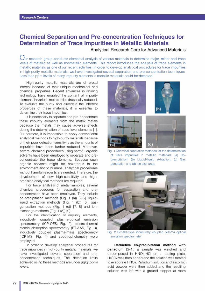
Research Centers
77 IMR KINKEN Research Highlights 2013 IMR KINKEN Research Highlights 2013
High-purity metallic materials are of broad interest because of their unique mechanical and chemical properties. Recent advances in refining technology have enabled the content of impurity elements in various metals to be drastically reduced. To evaluate the purity and elucidate the inherent properties of these materials, it is essential to determine their trace impurities.
It is necessary to separate and pre-concentrate these impurity elements from the matrix metals because the metals may cause adverse effects during the determination of trace-level elements [1]. Furthermore, it is impossible to apply conventional analytical methods to high-purity materials because of their poor detection sensitivity as the amounts of impurities have been further reduced. Moreover, several chemical procedures using harmful organic solvents have been employed to separate and pre-concentrate the trace elements. Because such organic solvents might be hazardous to the environment and to humans, analytical procedures without harmful reagents are needed. Therefore, the development of new high-sensitivity and high-precision analytical methods are required.
For trace analysis of metal samples, several chemical procedures for separation and pre-concentration have been employed. They include co-precipitation methods (Fig. 1 (a)) [2-5], liquid-liquid extraction methods (Fig. 1 (b)) [6], gas-generation methods (Fig. 1 (c)) [7, 8] and ion-exchange methods (Fig. 1 (d)) [9].
For the identification of impurity elements, inductively coupled plasma-optical emission spectrometry (ICP-OES, Fig. 2), electro-thermal atomic absorption spectrometry (ET-AAS, Fig. 3), inductively coupled plasma-mass spectrometry (ICP-MS, Fig. 4) and spectrophotometry were employed.
In order to develop analytical procedures for trace impurities in high-purity metallic materials, we have investigated several separation and pre-concentration techniques. The detection limits achieved using these methods are under μg/g (ppm) levels.
Reductive co-precipitation method with palladium [2-4]: a sample was weighed and decomposed in HNO3-HCl on a heating plate. H2SO4 was then added and the solution was heated to evaporate HNO3. Palladium solution and ascorbic acid powder were then added and the resulting solution was left with a ground stopper at room
Chemical Separation and Pre-concentration Techniques for Determination of Trace Impurities in Metallic Materials
Analytical Research Core for Advanced Materials
Our research group conducts elemental analysis of various materials to determine major, minor and trace levels of metallic as well as nonmetallic elements. This report introduces the analysis of trace elements in metallic materials as one of our recent activities. In order to develop analytical procedures for trace impurities in high-purity metallic materials, we have investigated several separation and pre-concentration techniques. Less than ppm levels of many impurity elements in metallic materials could be detected.
Fig. 1 Chemical separation methods for the determination of trace impurities in metallic materials: (a) Co-precipitation, (b) Liquid-liquid extraction, (c) Gas generation and (d) Ion exchange
Fig. 2 Echelle-type inductively coupled plasma optical emission spectrometer

Research Centers
IMR KINKEN Research Highlights 2013
IMR KINKEN Research Highlights 2013
78IMR KINKEN Research Highlights 2013
temperature for more than 3 hours. After being allowed to rest, the precipitate was collected using a membrane filter. Immediately thereafter, the precipitate was dissolved in a HNO3-HCl mixture at room temperature. Finally, the solution was diluted with water.
Liquid-liquid extraction method using 4-methyl-2-pentanone [6]: a sample was weighed and decomposed in HNO3-HCl on a heating plate. After this, the solution was heated until dry. After cooling, the dried sample was dissolved and transferred into an extraction funnel using 5.4 mol/L of HCl. Then, 4-methyl-2-pentanone was added and the extraction funnel was agitated for 1-2 minutes. After separation of the organic and inorganic phases, the inorganic phase was transferred into a quartz beaker and evaporated on a heating plate. In order to decompose the 4-methyl-2-pentanone remaining in the inorganic phase completely, HNO3 was added and the solution was heated until dry. Finally, the solution was diluted with water.
Anion exchange method [9]: a sample was weighed and decomposed in HF-H2O2 on a heating plate. Next, the solution was diluted with 1 mol/L of HF and introduced into a column packed with anion-exchange resin. After 2 mol/L of HF was introduced into the column to remove the matrix iron, analytes were eluted using an eluant (HNO3-H2O2). H2SO4 was added to the eluant, subsequently heating to fumes. Finally, the solution was diluted with water.
By using the separation and pre-concentration method, the influence of matrix metals on the analysis by the analytical instruments described above is removed and the analytes in the sample solution can subsequently be concentrated. Consequently, it is possible to determine trace elements in metallic materials more sensitively and precisely.
References[1] K. Takada, T. Ashino, T. Syoji, T. Itagaki (Sato) and K.
Wagatsuma, Tetsu-To-Hagane, 93, 190 (2007).
[2] T. Ashino , K. Takada and K. Hirokawa, Anal. Chim. Acta 297,
443 (1994).
[3] T. Ashino and K. Takada, Anal. Chim. Acta 312, 157 (1995).
[4] T. Ashino and K. Takada, J. Anal. Atom. Spectrom. 11, 577
(1996).
[5] T. Itagaki, T. Ashino, K. Takada and K. Wagatsuma, Bunseki
Kagaku 59, 43 (2010).
[6] T. Ashino, K. Takada, K. Wagatsuma and K. Abiko, MATÉRIAUX
& TECHNIQUES, Numéro Hors Série-Décembre 31 (2003).
[7] M. Ishikuro and J. kimura, Bunseki Kagaku 37, 498 (1988).
[8] T. Ashino, K. Tozawa and K. Wagatsuma, Bunseki Kagaku 60,
175 (2011).
[9] F. Sakamoto, K. Takada and K. Wagatsuma, Bunseki Kagaku
54, 1037 (2005).
Tetsuya Ashino (Analytical research Core for Advanced materials)E-mail: [email protected]: http://bunseki-core.imr.tohoku.ac.jp/
Fig. 3 Continuous-light-source atomic absorption spectrometer
Fig. 4 Double-focused inductively coupled mass spectrometer

Research Centers
79 IMR KINKEN Research Highlights 2013 IMR KINKEN Research Highlights 2013
Necessity of a breakthrough in soft magnetic materials
There is an urgent demand for a soft magnetic material with a high saturation magnetic flux density (Bs) and low coercivity (Hc). However, it is hard to increase Bs without increasing Hc at the same time because Hc changes inversely to Bs. The soft magnetic Fe-Co and Fe-Ni based amorphous alloys are well known. These amorphous alloys exhibit permeabilities of an order of magnitude higher than pure iron but their saturated magnetic flux density is relatively low.
The present project aims to develop new Fe-based soft magnetic materials with the same Bs as for Fe-Si steels but with a lower magnetic core loss and a higher permeability.
The "NANOMET™": a new nanocrystalline soft magnetic material
"NANOMET™," a new soft magnetic alloy developed by our group, is made up of heterogeneous microstructures consisting of α-Fe grains (with size ~ 10 nm) which are surrounded by thin iron-metalloid phases. The production of "NANOMET™ " is very cost-effective because of the low materials cost (no rare earth elements) and the material's processing in air.
It is highly anticipated that "NANOMET™ " can be very effective at preventing energy loss in applications such as high-current electrical transformers and motors. At a saturated magnetic flux density of 1.5 T, "NANOMET™ " is able to reduce the magnetic core loss by over 90% in comparison to the commercial Fe-Si magnetic steels.
Significant Reduction in Transmission and Power Losses Through Development of Nanocrystalline Soft Magnetic MaterialsResearch and Development Center for Ultra High Efficiency Nanocrystalline Soft Magnetic Materials
The Research and Development Center for Ultra High Efficiency Nanocrystalline Soft Magnetic Materials was established in June 2012. This is one of the three programs that were started by the national project of MEXT and the Reconstruction Agency for Tohoku Innovative Materials Technology Initiatives for Reconstruction. We aim to develop novel nanocrystalline magnetic alloys, "NANOMET™," made from nanoheterostructures obtained after the crystallization of the amorphous phase. These alloys will be mass produced at low cost and are expected to exhibit superior magnetic properties. A platform is to be built to enable collaborative research. Professors, researchers and engineers with different skills from academia and industry will work together to find solutions to a number of basic scientific issues and technical problems involved in the commercialization of new magnetic materials with extremely low core loss. This center will also contribute to essential design guidelines in the field of nanocrystalline soft magnetic materials. Moreover, the multifaceted collaboration between government, industry and academia motivated by this center can lead to the blooming of industries in the Tohoku region.
Fig. 1 Roadmap of innovation for "NANOMET™." Fig. 2 Dependence of W on Bm of "NANOMET™."

Research Centers
IMR KINKEN Research Highlights 2013
IMR KINKEN Research Highlights 2013
80IMR KINKEN Research Highlights 2013
Creation of the nanoheteroamorphous microstructure
Single-phase Fe-based amorphous alloys have already been commercialized and are used as the precursors for the development of Fe-based nanocrystalline soft magnetic alloys. However, the Fe content of amorphous precursors is restricted to below 78 at%. A higher concentration of Fe in the alloy reduces its glass-forming ability. This low glass-forming ability leads to the precipitation of α-Fe grains with sizes ranging from a few tenths of nanometers to hundreds of nanometers, even in the as-quenched state. A nonuniform precipitation of crystalline grains leads to a significant deterioration in soft magnetic performance. By the careful selection and adjustment of constituent elements (Fe, Si, B, P, Cu; based on interfacial energy and heats of mixing) in the alloy, our group has created a new nanoheteroamorphous structure. The nanocrystallization of the alloy has been successfully controlled to form uniform nanocrystalline (grain size ~ 10-20 nm) soft magnetic Fe-Si-B-P-Cu alloys, "NANOMET™," with Fe content > 80 at%. This new alloy revealed superior soft magnetic performance compared to the Fe-Si magnetic steels.
Reduction of core lossThe magnetic core loss in transformers and
motors is approximately 3.4% of the total electrical power consumption (33.5 billion Kwh per year in Japan). This energy loss can be reduced by ~ 72% with the replacement of commercial Fe-Si magnetic steels by "NANOMET™ " as a core material.
Expected achievements for "NANOMET™"The present project aims to explore the minimum
core loss, commercialization of the wide "NANOMET™ " thin ribbons, development of the commercial process for the thick, bulk alloys using gas atomization and stacking-layered methods. Research into the basic magnetism, relationship between nanocrystalline microstructure and magnetic properties, mechanism of reduction in the core loss and optimization of metalloid contents is to be conducted to elucidate the theoretical understanding and the material designs of the new alloy systems. The mass production of the "NANOMET™ " materials is to be achieved to contribute to future energy savings.
Akihiro Makino (Research and Development Center for Ultra High Efficiency Nano-crystalline Soft Magnetic Materials)E-mail: [email protected]: http://nanoc.imr.tohoku.ac.jp/english/index.html
Fig. 3 Self-Assembly of heteroamorphous microstructures of FeSiBPCu nanocrystalline alloys
Fig. 4 Dedication of "NANOMET™ " to reduce power loss
IMR KINKEN Research Highlights 2013
2013
Index

82IMR KINKEN Research Highlights 2013
AAbe, Hiroaki 28Aoki, Dai 52Arima, Hiroshi 6Ashino, Tetsuya 78
BBoulon, Georges 68
CChiba, Akihiko 12
FFujita, Motoki 54Furuhara, Tadashi 4, 70
GGoto, Takashi 50
HHiraka, Haruhiro 20
IIguchi, Satoshi 42Inoue, Koji 44Ito, Akihiko 50
KKamikawa, Naoya 4Kashiwakura, Shunsuke 36Kato, Hidemi 30Katsui, Hirokazu 50Kawazoe, Yoshiyuki 24Kiguchi, Takanori 14Konno, J. Toyohiko 14Kutsukake, Kentaro 22
MMakino, Akihiro 60, 80Masahashi, Naoya 64Matsuoka, Takashi 46Matsuura, Masato 20Miyamoto, Goro 4Mohri, Tetsuo 16, 66
NNagai, Yasuyoshi 44Niinomi, Mitsuo 8Nojima, Tsutomu 74Nojiri, Hiroyuki 40, 68Nomura, Kentaro 38
Nozawa, Jun 10
OOguro, Hidetoshi 62Ohoyama, Kenji 20Orimo, Shin-ichi 32, 72
SSaitoh, Eiji 18Sasaki, Takahiko 42Sato, Kazuhisa 14Sato, Shigeo 36Sato, Toyoto 20, 32Satoh, Yuhki 28Shikama, Tatsuo 26, 58Shimizu, Yasuo 44Sugiyama, Kazumasa 6
TTakanashi, Koki 48
UUmetsu, Y. Rie 56
WWagatsuma, Kazuaki 36
YYamamura, Tomoo 76Yoshikawa, Akira 34
Name page Name page
Author Index

83 IMR KINKEN Research Highlights 2013
Aactinide 52all-electron mixed basis approach 24alloy 8, 14amorphous 56atom probe tomography 44
Bbiomedical 8, 12
CCasida equation 24ceramics 26chemical vapor deposition (cvd) 50colloid 10cryptocrystalline 6crystal growth 10, 22, 34
D3D structure 44defects 16deformation 4dielectric properties 42dispersion coefficients 24doping 10
Eelectrical properties 38electrical resistivity 56electron microscopy 28electronic material 42, 44, 50energetic material 18energy storage 32
FFermi surface 52first-principles calculations 16foam 30
Ggrain boundaries 22
Hheavy fermion 52high magnetic field 40high strength steel 16high-Tc cuprate 20hydroxyapatite 8
Iinstrumentation 40insulator 38ion beam analysis 26
Lluminescence 26
Mmagnetic properties 38, 48mass spectroscopy 36mechanical properties 4, 12, 28microstructure 30, 50
Nneutron scattering 20, 32, 54nitride 46
Oorganic 42
Ppair distribution function 6phase transformation 14piezoelectric 34porosity 30
Qquantum spin system 54
Rradiation effects 28, 34
Sscanning transmission electron microscopy (stem) 14solar cells 22spectroscopy 40spin dynamics 54spin fluctuation 20spin wave 18, 48spintronic 48spintronics 18steel 4superplasticity 12
Vvapor phase epitaxy (vpe) 46
Wwaste management 36
XXAFS 6x-ray diffraction (xrd) 46
Keyword page Keyword page
Keyword Index

IMR KINKEN Research Highlights 2013
Editors: Hiroaki Abe (IMR), Takashi Matsuoka (IMR), Gerrit E.W. Bauer (IMR), Atsushi Tsukazaki (IMR), Kozo Fujiwara (IMR), Yuichiro Koizumi (IMR), and Satoshi Iguchi (IMR)
Editorial Staff: Yoshiko Takahashi (IMR), Miori Kikuchi (IMR)
Printing: HOKUTO Corporation
Organization Institute for Materials Research Tohoku University 2-1-1 Katahira, Aoba-ku, Sendai 980-8577, Japan Tel. +81-(0)22-215-2144 Fax. +81-(0)22-215-2482
URL: http://www.imr.tohoku.ac.jp/E-mail: [email protected]
© IMR October 2013