Embed Size (px)
Citation preview
LM193-N, LM2903-N, LM293-N, LM393-N
www.ti.com SNOSBJ6D –MAY 2004–REVISED MAY 2004
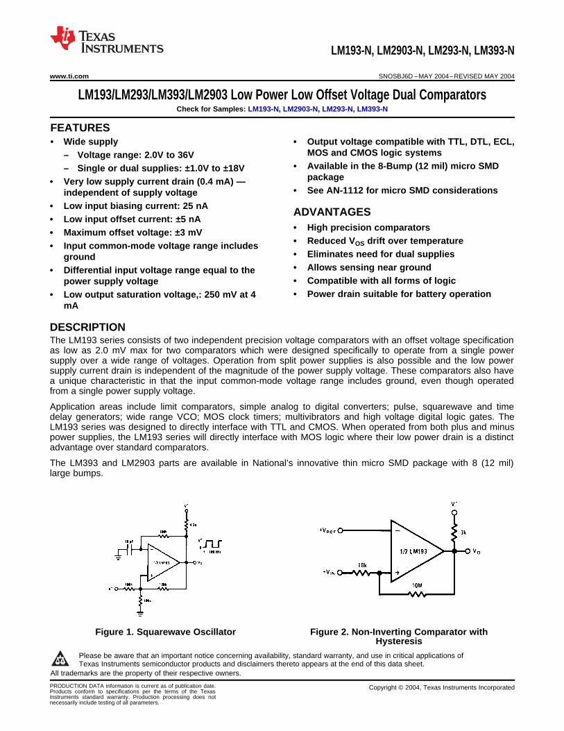
LM193/LM293/LM393/LM2903 Low Power Low Offset Voltage Dual ComparatorsCheck for Samples: LM193-N, LM2903-N, LM293-N, LM393-N
1FEATURES2• Wide supply • Output voltage compatible with TTL, DTL, ECL,
MOS and CMOS logic systems– Voltage range: 2.0V to 36V• Available in the 8-Bump (12 mil) micro SMD– Single or dual supplies: ±1.0V to ±18V
package• Very low supply current drain (0.4 mA) —• See AN-1112 for micro SMD considerationsindependent of supply voltage
• Low input biasing current: 25 nAADVANTAGES
• Low input offset current: ±5 nA• High precision comparators• Maximum offset voltage: ±3 mV• Reduced VOS drift over temperature• Input common-mode voltage range includes• Eliminates need for dual suppliesground• Allows sensing near ground• Differential input voltage range equal to the• Compatible with all forms of logicpower supply voltage• Power drain suitable for battery operation• Low output saturation voltage,: 250 mV at 4
mA
DESCRIPTIONThe LM193 series consists of two independent precision voltage comparators with an offset voltage specificationas low as 2.0 mV max for two comparators which were designed specifically to operate from a single powersupply over a wide range of voltages. Operation from split power supplies is also possible and the low powersupply current drain is independent of the magnitude of the power supply voltage. These comparators also havea unique characteristic in that the input common-mode voltage range includes ground, even though operatedfrom a single power supply voltage.
Application areas include limit comparators, simple analog to digital converters; pulse, squarewave and timedelay generators; wide range VCO; MOS clock timers; multivibrators and high voltage digital logic gates. TheLM193 series was designed to directly interface with TTL and CMOS. When operated from both plus and minuspower supplies, the LM193 series will directly interface with MOS logic where their low power drain is a distinctadvantage over standard comparators.
The LM393 and LM2903 parts are available in National’s innovative thin micro SMD package with 8 (12 mil)large bumps.
Figure 1. Squarewave Oscillator Figure 2. Non-Inverting Comparator withHysteresis
1
Please be aware that an important notice concerning availability, standard warranty, and use in critical applications ofTexas Instruments semiconductor products and disclaimers thereto appears at the end of this data sheet.
2All trademarks are the property of their respective owners.
PRODUCTION DATA information is current as of publication date. Copyright © 2004, Texas Instruments IncorporatedProducts conform to specifications per the terms of the TexasInstruments standard warranty. Production processing does notnecessarily include testing of all parameters.
LM193-N, LM2903-N, LM293-N, LM393-N
SNOSBJ6D –MAY 2004–REVISED MAY 2004 www.ti.com
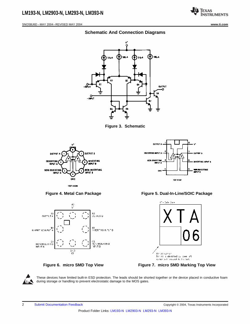
Schematic And Connection Diagrams
Figure 3. Schematic
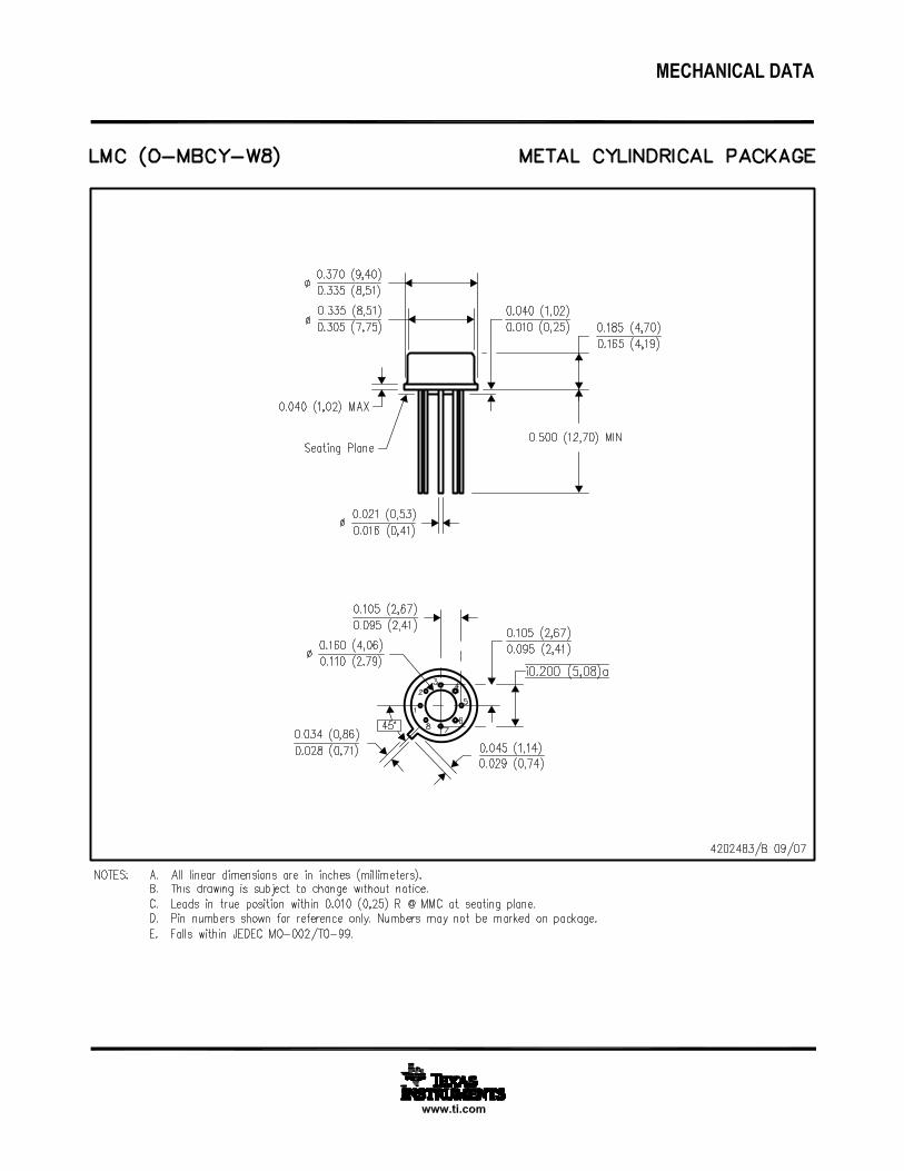
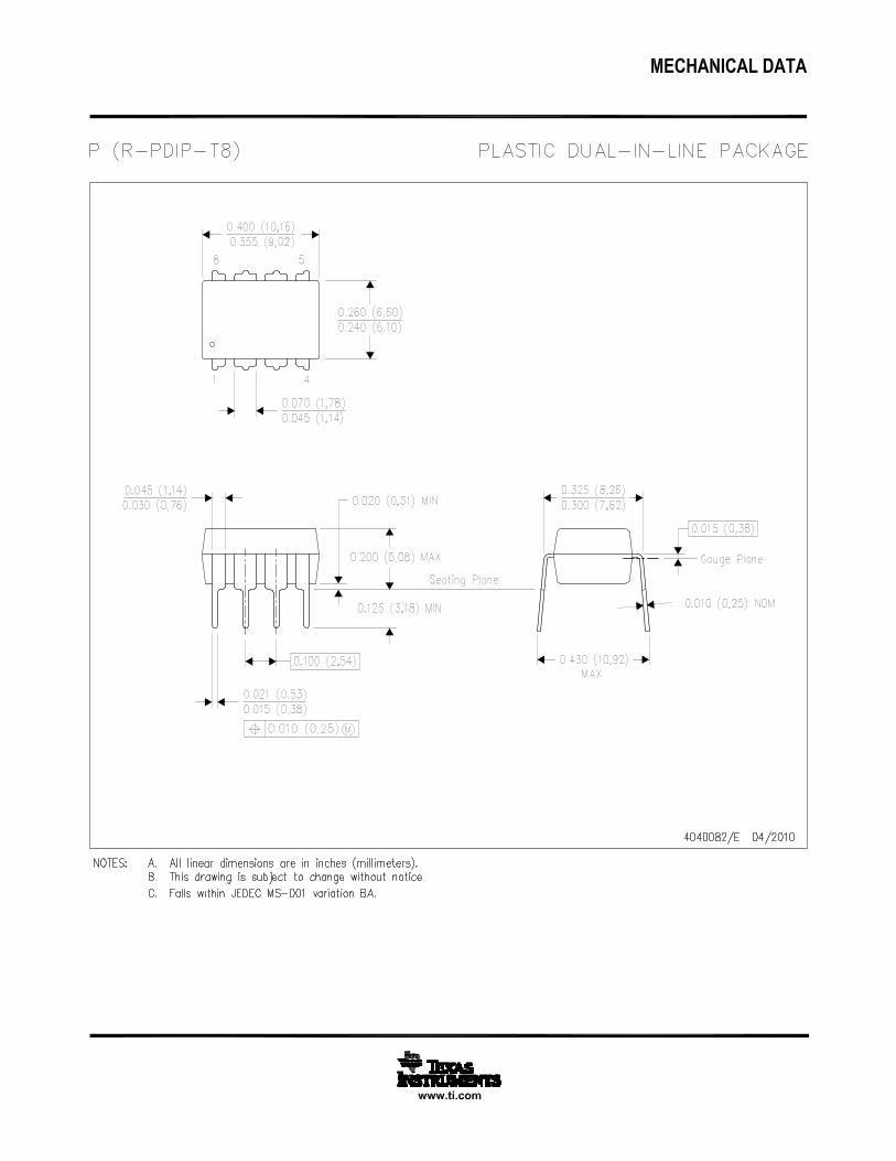
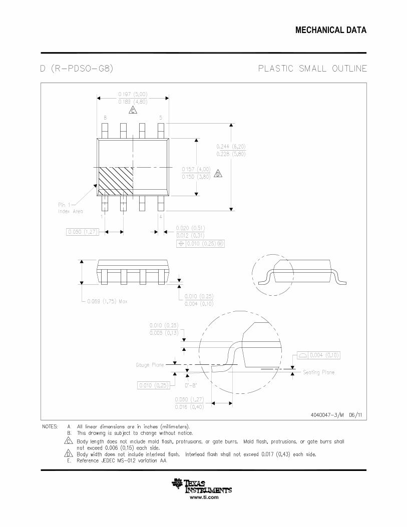
Figure 4. Metal Can Package Figure 5. Dual-In-Line/SOIC Package
Figure 6. micro SMD Top View Figure 7. micro SMD Marking Top View
These devices have limited built-in ESD protection. The leads should be shorted together or the device placed in conductive foamduring storage or handling to prevent electrostatic damage to the MOS gates.
2 Submit Documentation Feedback Copyright © 2004, Texas Instruments Incorporated
Product Folder Links: LM193-N LM2903-N LM293-N LM393-N
LM193-N, LM2903-N, LM293-N, LM393-N
www.ti.com SNOSBJ6D –MAY 2004–REVISED MAY 2004
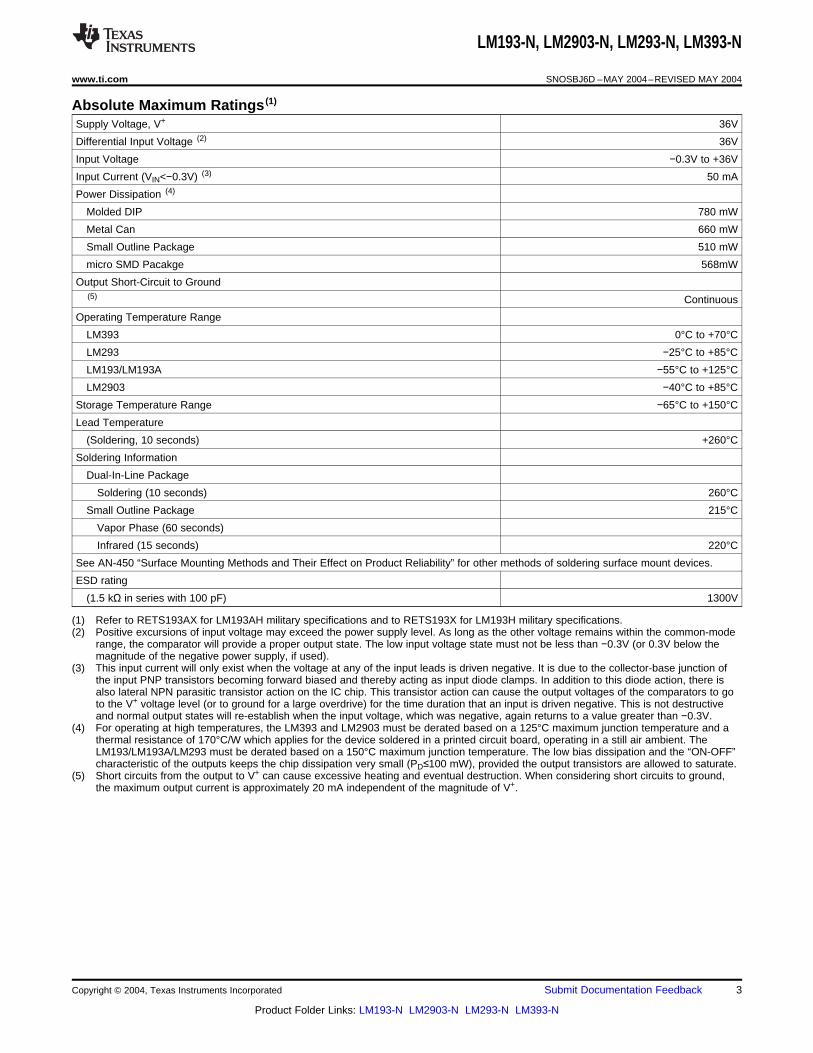
Absolute Maximum Ratings (1)
Supply Voltage, V+ 36V
Differential Input Voltage (2) 36V
Input Voltage −0.3V to +36V
Input Current (VIN<−0.3V) (3) 50 mA
Power Dissipation (4)
Molded DIP 780 mW
Metal Can 660 mW
Small Outline Package 510 mW
micro SMD Pacakge 568mW
Output Short-Circuit to Ground(5) Continuous
Operating Temperature Range
LM393 0°C to +70°C
LM293 −25°C to +85°C
LM193/LM193A −55°C to +125°C
LM2903 −40°C to +85°C
Storage Temperature Range −65°C to +150°C
Lead Temperature
(Soldering, 10 seconds) +260°C
Soldering Information
Dual-In-Line Package
Soldering (10 seconds) 260°C
Small Outline Package 215°C
Vapor Phase (60 seconds)
Infrared (15 seconds) 220°C
See AN-450 “Surface Mounting Methods and Their Effect on Product Reliability” for other methods of soldering surface mount devices.
ESD rating
(1.5 kΩ in series with 100 pF) 1300V
(1) Refer to RETS193AX for LM193AH military specifications and to RETS193X for LM193H military specifications.(2) Positive excursions of input voltage may exceed the power supply level. As long as the other voltage remains within the common-mode
range, the comparator will provide a proper output state. The low input voltage state must not be less than −0.3V (or 0.3V below themagnitude of the negative power supply, if used).
(3) This input current will only exist when the voltage at any of the input leads is driven negative. It is due to the collector-base junction ofthe input PNP transistors becoming forward biased and thereby acting as input diode clamps. In addition to this diode action, there isalso lateral NPN parasitic transistor action on the IC chip. This transistor action can cause the output voltages of the comparators to goto the V+ voltage level (or to ground for a large overdrive) for the time duration that an input is driven negative. This is not destructiveand normal output states will re-establish when the input voltage, which was negative, again returns to a value greater than −0.3V.
(4) For operating at high temperatures, the LM393 and LM2903 must be derated based on a 125°C maximum junction temperature and athermal resistance of 170°C/W which applies for the device soldered in a printed circuit board, operating in a still air ambient. TheLM193/LM193A/LM293 must be derated based on a 150°C maximum junction temperature. The low bias dissipation and the “ON-OFF”characteristic of the outputs keeps the chip dissipation very small (PD≤100 mW), provided the output transistors are allowed to saturate.
(5) Short circuits from the output to V+ can cause excessive heating and eventual destruction. When considering short circuits to ground,the maximum output current is approximately 20 mA independent of the magnitude of V+.
Copyright © 2004, Texas Instruments Incorporated Submit Documentation Feedback 3
Product Folder Links: LM193-N LM2903-N LM293-N LM393-N
LM193-N, LM2903-N, LM293-N, LM393-N
SNOSBJ6D –MAY 2004–REVISED MAY 2004 www.ti.com
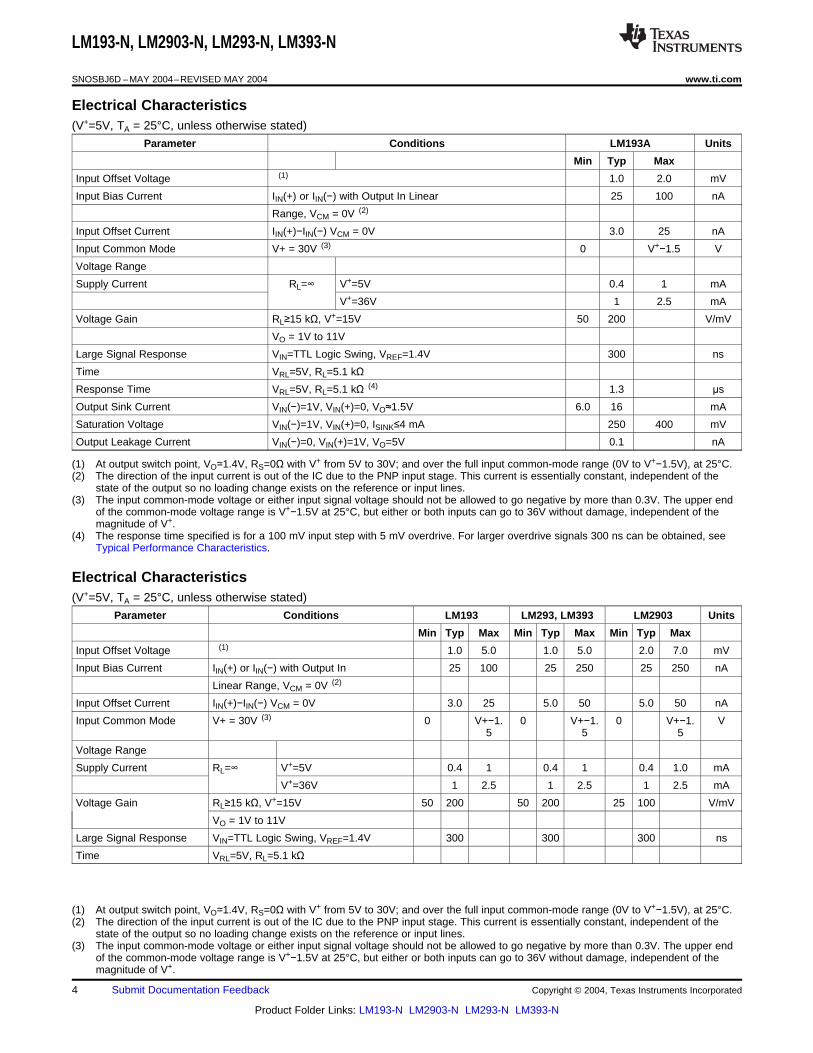
Electrical Characteristics(V+=5V, TA = 25°C, unless otherwise stated)
Parameter Conditions LM193A Units
Min Typ Max
Input Offset Voltage (1) 1.0 2.0 mV
Input Bias Current IIN(+) or IIN(−) with Output In Linear 25 100 nA
Range, VCM = 0V (2)
Input Offset Current IIN(+)−IIN(−) VCM = 0V 3.0 25 nA
Input Common Mode V+ = 30V (3) 0 V+−1.5 V
Voltage Range
Supply Current RL=∞ V+=5V 0.4 1 mA
V+=36V 1 2.5 mA
Voltage Gain RL≥15 kΩ, V+=15V 50 200 V/mV
VO = 1V to 11V
Large Signal Response VIN=TTL Logic Swing, VREF=1.4V 300 ns
Time VRL=5V, RL=5.1 kΩResponse Time VRL=5V, RL=5.1 kΩ (4) 1.3 μs
Output Sink Current VIN(−)=1V, VIN(+)=0, VO≈1.5V 6.0 16 mA
Saturation Voltage VIN(−)=1V, VIN(+)=0, ISINK≤4 mA 250 400 mV
Output Leakage Current VIN(−)=0, VIN(+)=1V, VO=5V 0.1 nA
(1) At output switch point, VO≃1.4V, RS=0Ω with V+ from 5V to 30V; and over the full input common-mode range (0V to V+−1.5V), at 25°C.(2) The direction of the input current is out of the IC due to the PNP input stage. This current is essentially constant, independent of the
state of the output so no loading change exists on the reference or input lines.(3) The input common-mode voltage or either input signal voltage should not be allowed to go negative by more than 0.3V. The upper end
of the common-mode voltage range is V+−1.5V at 25°C, but either or both inputs can go to 36V without damage, independent of themagnitude of V+.
(4) The response time specified is for a 100 mV input step with 5 mV overdrive. For larger overdrive signals 300 ns can be obtained, seeTypical Performance Characteristics.
Electrical Characteristics(V+=5V, TA = 25°C, unless otherwise stated)
Parameter Conditions LM193 LM293, LM393 LM2903 Units
Min Typ Max Min Typ Max Min Typ Max
Input Offset Voltage (1) 1.0 5.0 1.0 5.0 2.0 7.0 mV
Input Bias Current IIN(+) or IIN(−) with Output In 25 100 25 250 25 250 nA
Linear Range, VCM = 0V (2)
Input Offset Current IIN(+)−IIN(−) VCM = 0V 3.0 25 5.0 50 5.0 50 nA
Input Common Mode V+ = 30V (3) 0 V+−1. 0 V+−1. 0 V+−1. V5 5 5
Voltage Range
Supply Current RL=∞ V+=5V 0.4 1 0.4 1 0.4 1.0 mA
V+=36V 1 2.5 1 2.5 1 2.5 mA
Voltage Gain RL≥15 kΩ, V+=15V 50 200 50 200 25 100 V/mV
VO = 1V to 11V
Large Signal Response VIN=TTL Logic Swing, VREF=1.4V 300 300 300 ns
Time VRL=5V, RL=5.1 kΩ
(1) At output switch point, VO≃1.4V, RS=0Ω with V+ from 5V to 30V; and over the full input common-mode range (0V to V+−1.5V), at 25°C.(2) The direction of the input current is out of the IC due to the PNP input stage. This current is essentially constant, independent of the
state of the output so no loading change exists on the reference or input lines.(3) The input common-mode voltage or either input signal voltage should not be allowed to go negative by more than 0.3V. The upper end
of the common-mode voltage range is V+−1.5V at 25°C, but either or both inputs can go to 36V without damage, independent of themagnitude of V+.
4 Submit Documentation Feedback Copyright © 2004, Texas Instruments Incorporated
Product Folder Links: LM193-N LM2903-N LM293-N LM393-N
LM193-N, LM2903-N, LM293-N, LM393-N
www.ti.com SNOSBJ6D –MAY 2004–REVISED MAY 2004
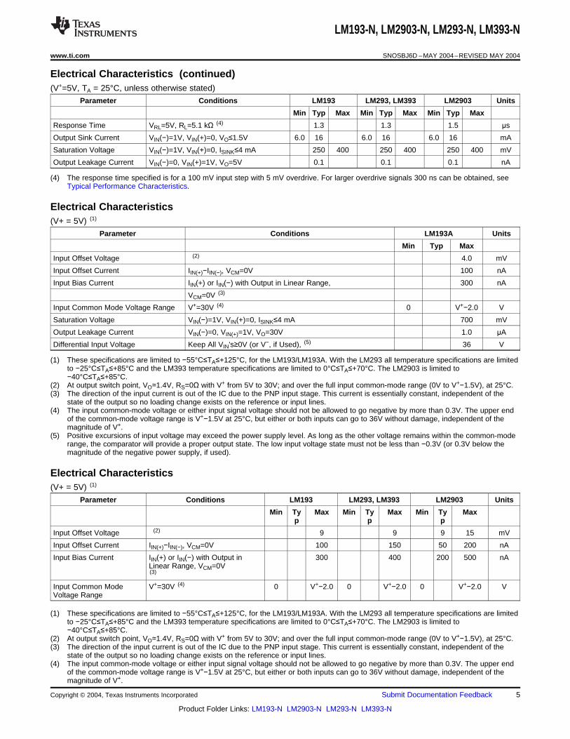
Electrical Characteristics (continued)(V+=5V, TA = 25°C, unless otherwise stated)
Parameter Conditions LM193 LM293, LM393 LM2903 Units
Min Typ Max Min Typ Max Min Typ Max
Response Time VRL=5V, RL=5.1 kΩ (4) 1.3 1.3 1.5 μs
Output Sink Current VIN(−)=1V, VIN(+)=0, VO≤1.5V 6.0 16 6.0 16 6.0 16 mA
Saturation Voltage VIN(−)=1V, VIN(+)=0, ISINK≤4 mA 250 400 250 400 250 400 mV
Output Leakage Current VIN(−)=0, VIN(+)=1V, VO=5V 0.1 0.1 0.1 nA
(4) The response time specified is for a 100 mV input step with 5 mV overdrive. For larger overdrive signals 300 ns can be obtained, seeTypical Performance Characteristics.
Electrical Characteristics(V+ = 5V) (1)
Parameter Conditions LM193A Units
Min Typ Max
Input Offset Voltage (2) 4.0 mV
Input Offset Current IIN(+)−IIN(−), VCM=0V 100 nA
Input Bias Current IIN(+) or IIN(−) with Output in Linear Range, 300 nA
VCM=0V (3)
Input Common Mode Voltage Range V+=30V (4) 0 V+−2.0 V
Saturation Voltage VIN(−)=1V, VIN(+)=0, ISINK≤4 mA 700 mV
Output Leakage Current VIN(−)=0, VIN(+)=1V, VO=30V 1.0 μA
Differential Input Voltage Keep All VIN's≥0V (or V−, if Used), (5) 36 V
(1) These specifications are limited to −55°C≤TA≤+125°C, for the LM193/LM193A. With the LM293 all temperature specifications are limitedto −25°C≤TA≤+85°C and the LM393 temperature specifications are limited to 0°C≤TA≤+70°C. The LM2903 is limited to−40°C≤TA≤+85°C.
(2) At output switch point, VO≃1.4V, RS=0Ω with V+ from 5V to 30V; and over the full input common-mode range (0V to V+−1.5V), at 25°C.(3) The direction of the input current is out of the IC due to the PNP input stage. This current is essentially constant, independent of the
state of the output so no loading change exists on the reference or input lines.(4) The input common-mode voltage or either input signal voltage should not be allowed to go negative by more than 0.3V. The upper end
of the common-mode voltage range is V+−1.5V at 25°C, but either or both inputs can go to 36V without damage, independent of themagnitude of V+.
(5) Positive excursions of input voltage may exceed the power supply level. As long as the other voltage remains within the common-moderange, the comparator will provide a proper output state. The low input voltage state must not be less than −0.3V (or 0.3V below themagnitude of the negative power supply, if used).
Electrical Characteristics(V+ = 5V) (1)
Parameter Conditions LM193 LM293, LM393 LM2903 Units
Min Ty Max Min Ty Max Min Ty Maxp p p
Input Offset Voltage (2) 9 9 9 15 mV
Input Offset Current IIN(+)−IIN(−), VCM=0V 100 150 50 200 nA
Input Bias Current IIN(+) or IIN(−) with Output in 300 400 200 500 nALinear Range, VCM=0V(3)
Input Common Mode V+=30V (4) 0 V+−2.0 0 V+−2.0 0 V+−2.0 VVoltage Range
(1) These specifications are limited to −55°C≤TA≤+125°C, for the LM193/LM193A. With the LM293 all temperature specifications are limitedto −25°C≤TA≤+85°C and the LM393 temperature specifications are limited to 0°C≤TA≤+70°C. The LM2903 is limited to−40°C≤TA≤+85°C.
(2) At output switch point, VO≃1.4V, RS=0Ω with V+ from 5V to 30V; and over the full input common-mode range (0V to V+−1.5V), at 25°C.(3) The direction of the input current is out of the IC due to the PNP input stage. This current is essentially constant, independent of the
state of the output so no loading change exists on the reference or input lines.(4) The input common-mode voltage or either input signal voltage should not be allowed to go negative by more than 0.3V. The upper end
of the common-mode voltage range is V+−1.5V at 25°C, but either or both inputs can go to 36V without damage, independent of themagnitude of V+.
Copyright © 2004, Texas Instruments Incorporated Submit Documentation Feedback 5
Product Folder Links: LM193-N LM2903-N LM293-N LM393-N
LM193-N, LM2903-N, LM293-N, LM393-N
SNOSBJ6D –MAY 2004–REVISED MAY 2004 www.ti.com
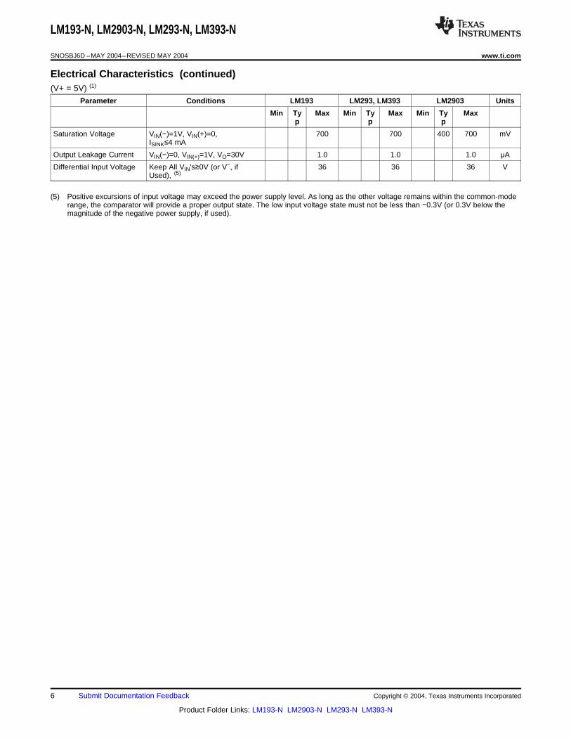
Electrical Characteristics (continued)(V+ = 5V) (1)
Parameter Conditions LM193 LM293, LM393 LM2903 Units
Min Ty Max Min Ty Max Min Ty Maxp p p
Saturation Voltage VIN(−)=1V, VIN(+)=0, 700 700 400 700 mVISINK≤4 mA
Output Leakage Current VIN(−)=0, VIN(+)=1V, VO=30V 1.0 1.0 1.0 μA
Differential Input Voltage Keep All VIN's≥0V (or V−, if 36 36 36 VUsed), (5)
(5) Positive excursions of input voltage may exceed the power supply level. As long as the other voltage remains within the common-moderange, the comparator will provide a proper output state. The low input voltage state must not be less than −0.3V (or 0.3V below themagnitude of the negative power supply, if used).
6 Submit Documentation Feedback Copyright © 2004, Texas Instruments Incorporated
Product Folder Links: LM193-N LM2903-N LM293-N LM393-N
LM193-N, LM2903-N, LM293-N, LM393-N
www.ti.com SNOSBJ6D –MAY 2004–REVISED MAY 2004
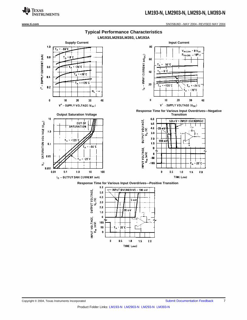
Typical Performance CharacteristicsLM193/LM293/LM393, LM193A
Supply Current Input Current
Response Time for Various Input Overdrives—NegativeOutput Saturation Voltage Transition
Response Time for Various Input Overdrives—Positive Transition
Copyright © 2004, Texas Instruments Incorporated Submit Documentation Feedback 7
Product Folder Links: LM193-N LM2903-N LM293-N LM393-N
LM193-N, LM2903-N, LM293-N, LM393-N
SNOSBJ6D –MAY 2004–REVISED MAY 2004 www.ti.com
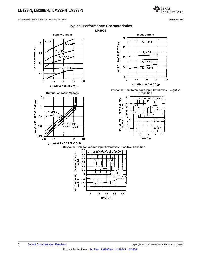
Typical Performance CharacteristicsLM2903
Supply Current Input Current
Response Time for Various Input Overdrives—NegativeOutput Saturation Voltage Transition
Response Time for Various Input Overdrives—Positive Transition
8 Submit Documentation Feedback Copyright © 2004, Texas Instruments Incorporated
Product Folder Links: LM193-N LM2903-N LM293-N LM393-N
LM193-N, LM2903-N, LM293-N, LM393-N
www.ti.com SNOSBJ6D –MAY 2004–REVISED MAY 2004
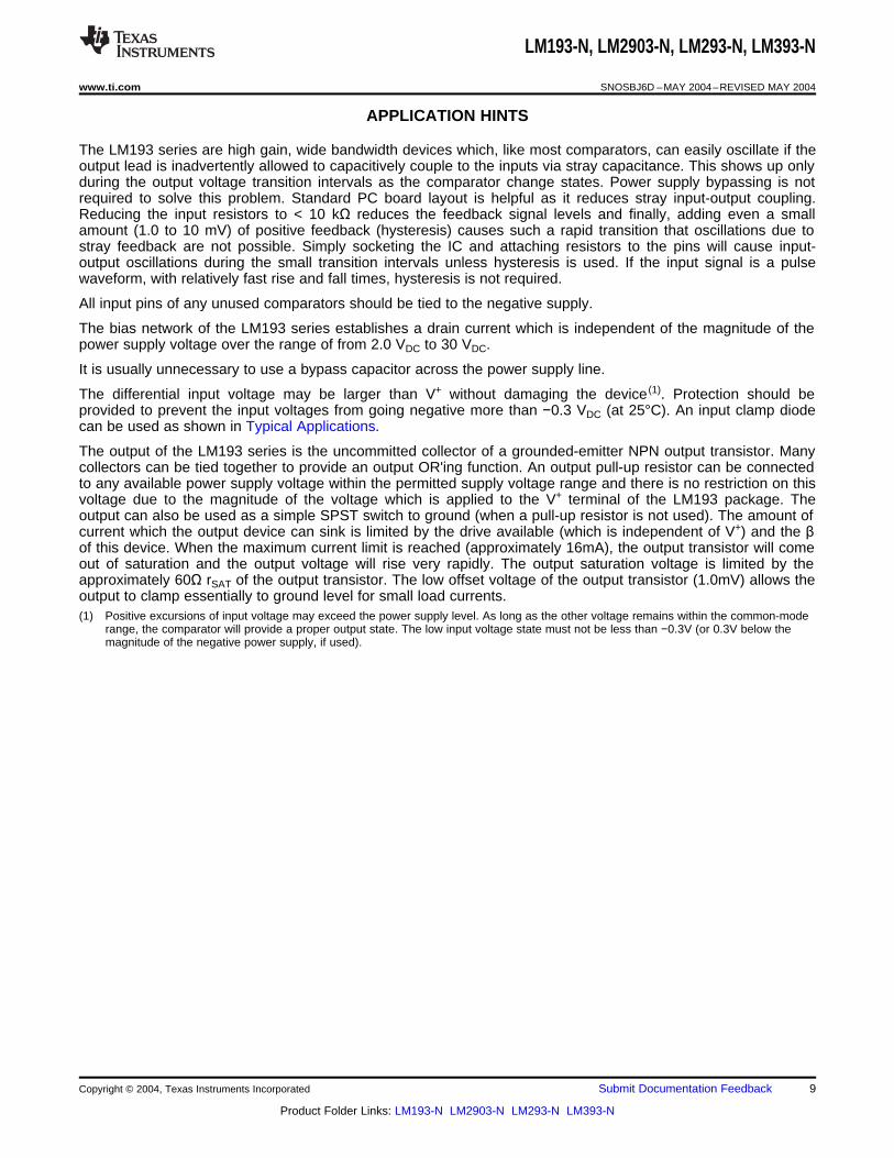
APPLICATION HINTS
The LM193 series are high gain, wide bandwidth devices which, like most comparators, can easily oscillate if theoutput lead is inadvertently allowed to capacitively couple to the inputs via stray capacitance. This shows up onlyduring the output voltage transition intervals as the comparator change states. Power supply bypassing is notrequired to solve this problem. Standard PC board layout is helpful as it reduces stray input-output coupling.Reducing the input resistors to < 10 kΩ reduces the feedback signal levels and finally, adding even a smallamount (1.0 to 10 mV) of positive feedback (hysteresis) causes such a rapid transition that oscillations due tostray feedback are not possible. Simply socketing the IC and attaching resistors to the pins will cause input-output oscillations during the small transition intervals unless hysteresis is used. If the input signal is a pulsewaveform, with relatively fast rise and fall times, hysteresis is not required.
All input pins of any unused comparators should be tied to the negative supply.
The bias network of the LM193 series establishes a drain current which is independent of the magnitude of thepower supply voltage over the range of from 2.0 VDC to 30 VDC.
It is usually unnecessary to use a bypass capacitor across the power supply line.
The differential input voltage may be larger than V+ without damaging the device (1). Protection should beprovided to prevent the input voltages from going negative more than −0.3 VDC (at 25°C). An input clamp diodecan be used as shown in Typical Applications.
The output of the LM193 series is the uncommitted collector of a grounded-emitter NPN output transistor. Manycollectors can be tied together to provide an output OR'ing function. An output pull-up resistor can be connectedto any available power supply voltage within the permitted supply voltage range and there is no restriction on thisvoltage due to the magnitude of the voltage which is applied to the V+ terminal of the LM193 package. Theoutput can also be used as a simple SPST switch to ground (when a pull-up resistor is not used). The amount ofcurrent which the output device can sink is limited by the drive available (which is independent of V+) and the βof this device. When the maximum current limit is reached (approximately 16mA), the output transistor will comeout of saturation and the output voltage will rise very rapidly. The output saturation voltage is limited by theapproximately 60Ω rSAT of the output transistor. The low offset voltage of the output transistor (1.0mV) allows theoutput to clamp essentially to ground level for small load currents.(1) Positive excursions of input voltage may exceed the power supply level. As long as the other voltage remains within the common-mode
range, the comparator will provide a proper output state. The low input voltage state must not be less than −0.3V (or 0.3V below themagnitude of the negative power supply, if used).
Copyright © 2004, Texas Instruments Incorporated Submit Documentation Feedback 9
Product Folder Links: LM193-N LM2903-N LM293-N LM393-N
LM193-N, LM2903-N, LM293-N, LM393-N
SNOSBJ6D –MAY 2004–REVISED MAY 2004 www.ti.com
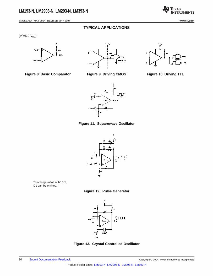
TYPICAL APPLICATIONS
(V+=5.0 VDC)
Figure 8. Basic Comparator Figure 9. Driving CMOS Figure 10. Driving TTL
Figure 11. Squarewave Oscillator
* For large ratios of R1/R2,D1 can be omitted.
Figure 12. Pulse Generator
Figure 13. Crystal Controlled Oscillator
10 Submit Documentation Feedback Copyright © 2004, Texas Instruments Incorporated
Product Folder Links: LM193-N LM2903-N LM293-N LM393-N
LM193-N, LM2903-N, LM293-N, LM393-N
www.ti.com SNOSBJ6D –MAY 2004–REVISED MAY 2004
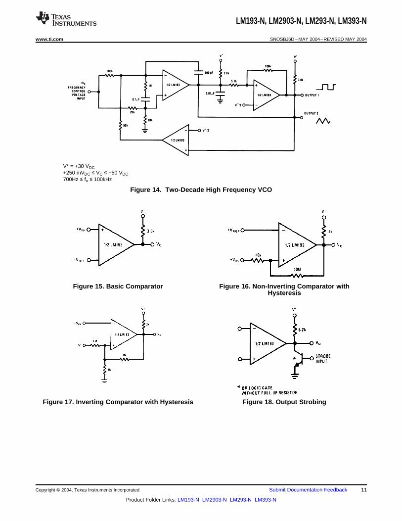
V* = +30 VDC+250 mVDC ≤ VC ≤ +50 VDC700Hz ≤ fo ≤ 100kHz
Figure 14. Two-Decade High Frequency VCO
Figure 15. Basic Comparator Figure 16. Non-Inverting Comparator withHysteresis
Figure 17. Inverting Comparator with Hysteresis Figure 18. Output Strobing
Copyright © 2004, Texas Instruments Incorporated Submit Documentation Feedback 11
Product Folder Links: LM193-N LM2903-N LM293-N LM393-N
LM193-N, LM2903-N, LM293-N, LM393-N
SNOSBJ6D –MAY 2004–REVISED MAY 2004 www.ti.com
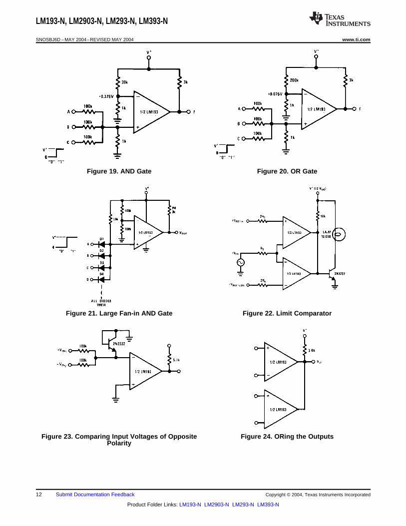
Figure 19. AND Gate Figure 20. OR Gate
Figure 21. Large Fan-in AND Gate Figure 22. Limit Comparator
Figure 23. Comparing Input Voltages of Opposite Figure 24. ORing the OutputsPolarity
12 Submit Documentation Feedback Copyright © 2004, Texas Instruments Incorporated
Product Folder Links: LM193-N LM2903-N LM293-N LM393-N
LM193-N, LM2903-N, LM293-N, LM393-N
www.ti.com SNOSBJ6D –MAY 2004–REVISED MAY 2004
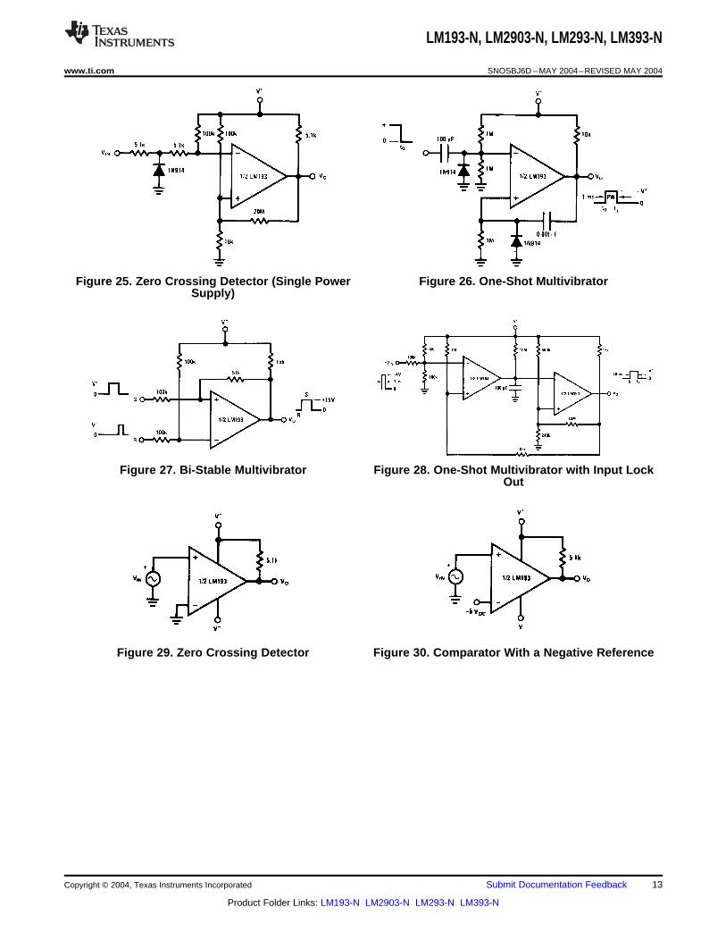
Figure 25. Zero Crossing Detector (Single Power Figure 26. One-Shot MultivibratorSupply)
Figure 27. Bi-Stable Multivibrator Figure 28. One-Shot Multivibrator with Input LockOut
Figure 29. Zero Crossing Detector Figure 30. Comparator With a Negative Reference
Copyright © 2004, Texas Instruments Incorporated Submit Documentation Feedback 13
Product Folder Links: LM193-N LM2903-N LM293-N LM393-N
LM193-N, LM2903-N, LM293-N, LM393-N
SNOSBJ6D –MAY 2004–REVISED MAY 2004 www.ti.com
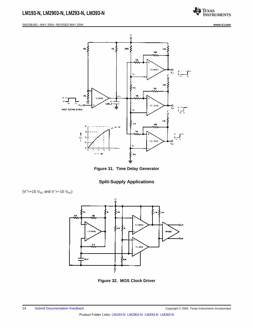
Figure 31. Time Delay Generator
Split-Supply Applications
(V+=+15 VDC and V−=−15 VDC)
Figure 32. MOS Clock Driver
14 Submit Documentation Feedback Copyright © 2004, Texas Instruments Incorporated
Product Folder Links: LM193-N LM2903-N LM293-N LM393-N
PACKAGE OPTION ADDENDUM
www.ti.com 16-Nov-2012
Addendum-Page 1
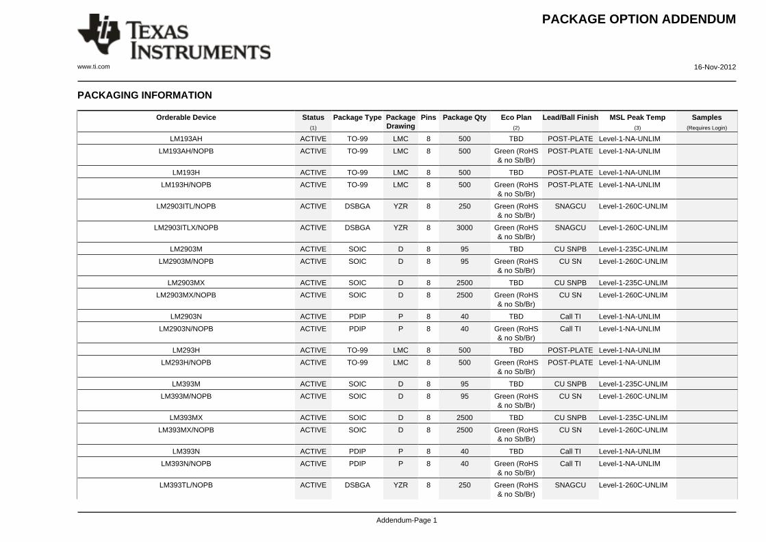
PACKAGING INFORMATION
Orderable Device Status(1)
Package Type PackageDrawing
Pins Package Qty Eco Plan(2)
Lead/Ball Finish MSL Peak Temp(3)
Samples(Requires Login)
LM193AH ACTIVE TO-99 LMC 8 500 TBD POST-PLATE Level-1-NA-UNLIM
LM193AH/NOPB ACTIVE TO-99 LMC 8 500 Green (RoHS& no Sb/Br)
POST-PLATE Level-1-NA-UNLIM
LM193H ACTIVE TO-99 LMC 8 500 TBD POST-PLATE Level-1-NA-UNLIM
LM193H/NOPB ACTIVE TO-99 LMC 8 500 Green (RoHS& no Sb/Br)
POST-PLATE Level-1-NA-UNLIM
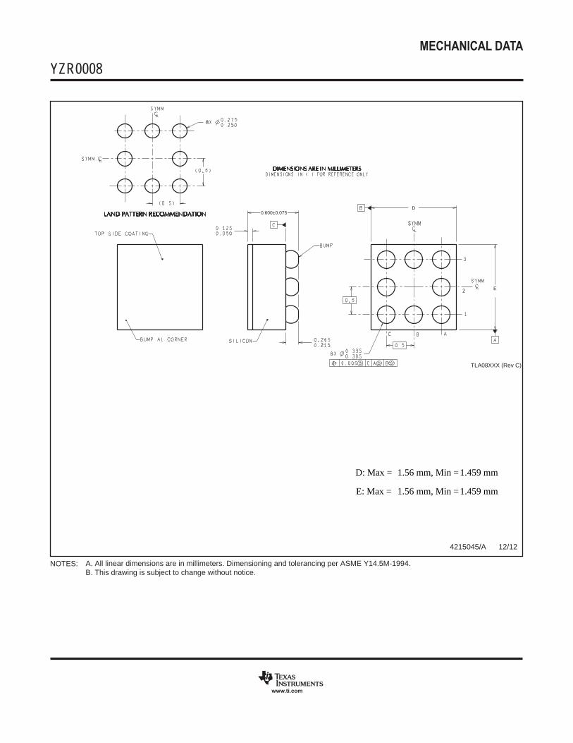
LM2903ITL/NOPB ACTIVE DSBGA YZR 8 250 Green (RoHS& no Sb/Br)
SNAGCU Level-1-260C-UNLIM
LM2903ITLX/NOPB ACTIVE DSBGA YZR 8 3000 Green (RoHS& no Sb/Br)
SNAGCU Level-1-260C-UNLIM
LM2903M ACTIVE SOIC D 8 95 TBD CU SNPB Level-1-235C-UNLIM
LM2903M/NOPB ACTIVE SOIC D 8 95 Green (RoHS& no Sb/Br)
CU SN Level-1-260C-UNLIM
LM2903MX ACTIVE SOIC D 8 2500 TBD CU SNPB Level-1-235C-UNLIM
LM2903MX/NOPB ACTIVE SOIC D 8 2500 Green (RoHS& no Sb/Br)
CU SN Level-1-260C-UNLIM
LM2903N ACTIVE PDIP P 8 40 TBD Call TI Level-1-NA-UNLIM
LM2903N/NOPB ACTIVE PDIP P 8 40 Green (RoHS& no Sb/Br)
Call TI Level-1-NA-UNLIM
LM293H ACTIVE TO-99 LMC 8 500 TBD POST-PLATE Level-1-NA-UNLIM
LM293H/NOPB ACTIVE TO-99 LMC 8 500 Green (RoHS& no Sb/Br)
POST-PLATE Level-1-NA-UNLIM
LM393M ACTIVE SOIC D 8 95 TBD CU SNPB Level-1-235C-UNLIM
LM393M/NOPB ACTIVE SOIC D 8 95 Green (RoHS& no Sb/Br)
CU SN Level-1-260C-UNLIM
LM393MX ACTIVE SOIC D 8 2500 TBD CU SNPB Level-1-235C-UNLIM
LM393MX/NOPB ACTIVE SOIC D 8 2500 Green (RoHS& no Sb/Br)
CU SN Level-1-260C-UNLIM
LM393N ACTIVE PDIP P 8 40 TBD Call TI Level-1-NA-UNLIM
LM393N/NOPB ACTIVE PDIP P 8 40 Green (RoHS& no Sb/Br)
Call TI Level-1-NA-UNLIM
LM393TL/NOPB ACTIVE DSBGA YZR 8 250 Green (RoHS& no Sb/Br)
SNAGCU Level-1-260C-UNLIM
PACKAGE OPTION ADDENDUM
www.ti.com 16-Nov-2012
Addendum-Page 2
Orderable Device Status(1)
Package Type PackageDrawing
Pins Package Qty Eco Plan(2)
Lead/Ball Finish MSL Peak Temp(3)
Samples(Requires Login)
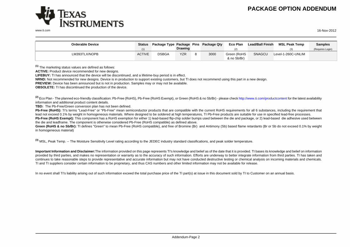
LM393TLX/NOPB ACTIVE DSBGA YZR 8 3000 Green (RoHS& no Sb/Br)
SNAGCU Level-1-260C-UNLIM
(1) The marketing status values are defined as follows:ACTIVE: Product device recommended for new designs.LIFEBUY: TI has announced that the device will be discontinued, and a lifetime-buy period is in effect.NRND: Not recommended for new designs. Device is in production to support existing customers, but TI does not recommend using this part in a new design.PREVIEW: Device has been announced but is not in production. Samples may or may not be available.OBSOLETE: TI has discontinued the production of the device.
(2) Eco Plan - The planned eco-friendly classification: Pb-Free (RoHS), Pb-Free (RoHS Exempt), or Green (RoHS & no Sb/Br) - please check http://www.ti.com/productcontent for the latest availabilityinformation and additional product content details.TBD: The Pb-Free/Green conversion plan has not been defined.Pb-Free (RoHS): TI's terms "Lead-Free" or "Pb-Free" mean semiconductor products that are compatible with the current RoHS requirements for all 6 substances, including the requirement thatlead not exceed 0.1% by weight in homogeneous materials. Where designed to be soldered at high temperatures, TI Pb-Free products are suitable for use in specified lead-free processes.Pb-Free (RoHS Exempt): This component has a RoHS exemption for either 1) lead-based flip-chip solder bumps used between the die and package, or 2) lead-based die adhesive used betweenthe die and leadframe. The component is otherwise considered Pb-Free (RoHS compatible) as defined above.Green (RoHS & no Sb/Br): TI defines "Green" to mean Pb-Free (RoHS compatible), and free of Bromine (Br) and Antimony (Sb) based flame retardants (Br or Sb do not exceed 0.1% by weightin homogeneous material)
(3) MSL, Peak Temp. -- The Moisture Sensitivity Level rating according to the JEDEC industry standard classifications, and peak solder temperature.
Important Information and Disclaimer:The information provided on this page represents TI's knowledge and belief as of the date that it is provided. TI bases its knowledge and belief on informationprovided by third parties, and makes no representation or warranty as to the accuracy of such information. Efforts are underway to better integrate information from third parties. TI has taken andcontinues to take reasonable steps to provide representative and accurate information but may not have conducted destructive testing or chemical analysis on incoming materials and chemicals.TI and TI suppliers consider certain information to be proprietary, and thus CAS numbers and other limited information may not be available for release.
In no event shall TI's liability arising out of such information exceed the total purchase price of the TI part(s) at issue in this document sold by TI to Customer on an annual basis.
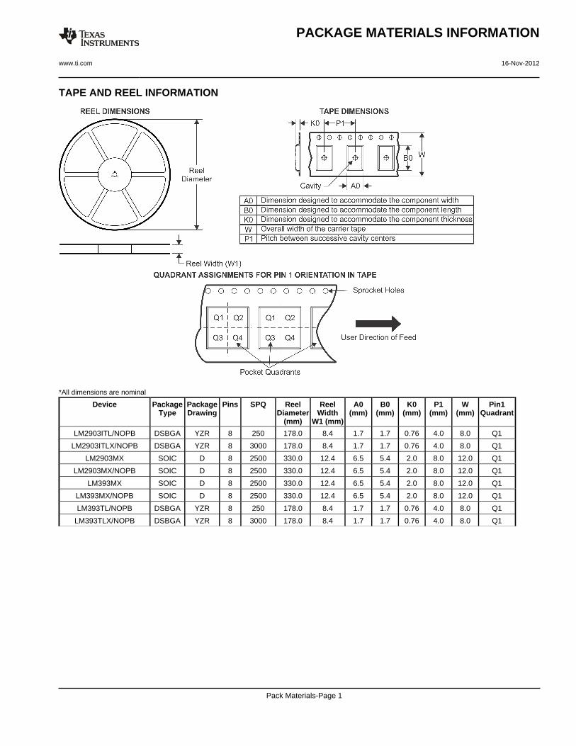
TAPE AND REEL INFORMATION
*All dimensions are nominal
Device PackageType
PackageDrawing
Pins SPQ ReelDiameter
(mm)
ReelWidth
W1 (mm)
A0(mm)
B0(mm)
K0(mm)
P1(mm)
W(mm)
Pin1Quadrant
LM2903ITL/NOPB DSBGA YZR 8 250 178.0 8.4 1.7 1.7 0.76 4.0 8.0 Q1
LM2903ITLX/NOPB DSBGA YZR 8 3000 178.0 8.4 1.7 1.7 0.76 4.0 8.0 Q1
LM2903MX SOIC D 8 2500 330.0 12.4 6.5 5.4 2.0 8.0 12.0 Q1
LM2903MX/NOPB SOIC D 8 2500 330.0 12.4 6.5 5.4 2.0 8.0 12.0 Q1
LM393MX SOIC D 8 2500 330.0 12.4 6.5 5.4 2.0 8.0 12.0 Q1
LM393MX/NOPB SOIC D 8 2500 330.0 12.4 6.5 5.4 2.0 8.0 12.0 Q1
LM393TL/NOPB DSBGA YZR 8 250 178.0 8.4 1.7 1.7 0.76 4.0 8.0 Q1
LM393TLX/NOPB DSBGA YZR 8 3000 178.0 8.4 1.7 1.7 0.76 4.0 8.0 Q1
PACKAGE MATERIALS INFORMATION
www.ti.com 16-Nov-2012
Pack Materials-Page 1
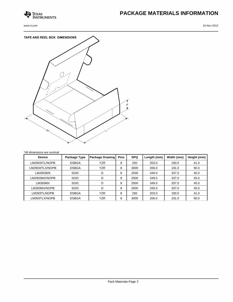
*All dimensions are nominal
Device Package Type Package Drawing Pins SPQ Length (mm) Width (mm) Height (mm)
LM2903ITL/NOPB DSBGA YZR 8 250 203.0 190.0 41.0
LM2903ITLX/NOPB DSBGA YZR 8 3000 206.0 191.0 90.0
LM2903MX SOIC D 8 2500 349.0 337.0 45.0
LM2903MX/NOPB SOIC D 8 2500 349.0 337.0 45.0
LM393MX SOIC D 8 2500 349.0 337.0 45.0
LM393MX/NOPB SOIC D 8 2500 349.0 337.0 45.0
LM393TL/NOPB DSBGA YZR 8 250 203.0 190.0 41.0
LM393TLX/NOPB DSBGA YZR 8 3000 206.0 191.0 90.0
PACKAGE MATERIALS INFORMATION
www.ti.com 16-Nov-2012
Pack Materials-Page 2
MECHANICAL DATA
YZR0008xxx
www.ti.com
TLA08XXX (Rev C)
0.600±0.075D
E
A. All linear dimensions are in millimeters. Dimensioning and tolerancing per ASME Y14.5M-1994.B. This drawing is subject to change without notice.
NOTES:
4215045/A 12/12
D: Max =
E: Max =
1.56 mm, Min =
1.56 mm, Min =
1.459 mm
1.459 mm
IMPORTANT NOTICE
Texas Instruments Incorporated and its subsidiaries (TI) reserve the right to make corrections, enhancements, improvements and otherchanges to its semiconductor products and services per JESD46, latest issue, and to discontinue any product or service per JESD48, latestissue. Buyers should obtain the latest relevant information before placing orders and should verify that such information is current andcomplete. All semiconductor products (also referred to herein as “components”) are sold subject to TI’s terms and conditions of salesupplied at the time of order acknowledgment.
TI warrants performance of its components to the specifications applicable at the time of sale, in accordance with the warranty in TI’s termsand conditions of sale of semiconductor products. Testing and other quality control techniques are used to the extent TI deems necessaryto support this warranty. Except where mandated by applicable law, testing of all parameters of each component is not necessarilyperformed.
TI assumes no liability for applications assistance or the design of Buyers’ products. Buyers are responsible for their products andapplications using TI components. To minimize the risks associated with Buyers’ products and applications, Buyers should provideadequate design and operating safeguards.
TI does not warrant or represent that any license, either express or implied, is granted under any patent right, copyright, mask work right, orother intellectual property right relating to any combination, machine, or process in which TI components or services are used. Informationpublished by TI regarding third-party products or services does not constitute a license to use such products or services or a warranty orendorsement thereof. Use of such information may require a license from a third party under the patents or other intellectual property of thethird party, or a license from TI under the patents or other intellectual property of TI.
Reproduction of significant portions of TI information in TI data books or data sheets is permissible only if reproduction is without alterationand is accompanied by all associated warranties, conditions, limitations, and notices. TI is not responsible or liable for such altereddocumentation. Information of third parties may be subject to additional restrictions.
Resale of TI components or services with statements different from or beyond the parameters stated by TI for that component or servicevoids all express and any implied warranties for the associated TI component or service and is an unfair and deceptive business practice.TI is not responsible or liable for any such statements.
Buyer acknowledges and agrees that it is solely responsible for compliance with all legal, regulatory and safety-related requirementsconcerning its products, and any use of TI components in its applications, notwithstanding any applications-related information or supportthat may be provided by TI. Buyer represents and agrees that it has all the necessary expertise to create and implement safeguards whichanticipate dangerous consequences of failures, monitor failures and their consequences, lessen the likelihood of failures that might causeharm and take appropriate remedial actions. Buyer will fully indemnify TI and its representatives against any damages arising out of the useof any TI components in safety-critical applications.
In some cases, TI components may be promoted specifically to facilitate safety-related applications. With such components, TI’s goal is tohelp enable customers to design and create their own end-product solutions that meet applicable functional safety standards andrequirements. Nonetheless, such components are subject to these terms.
No TI components are authorized for use in FDA Class III (or similar life-critical medical equipment) unless authorized officers of the partieshave executed a special agreement specifically governing such use.
Only those TI components which TI has specifically designated as military grade or “enhanced plastic” are designed and intended for use inmilitary/aerospace applications or environments. Buyer acknowledges and agrees that any military or aerospace use of TI componentswhich have not been so designated is solely at the Buyer's risk, and that Buyer is solely responsible for compliance with all legal andregulatory requirements in connection with such use.
TI has specifically designated certain components as meeting ISO/TS16949 requirements, mainly for automotive use. In any case of use ofnon-designated products, TI will not be responsible for any failure to meet ISO/TS16949.
Products Applications
Audio www.ti.com/audio Automotive and Transportation www.ti.com/automotive
Amplifiers amplifier.ti.com Communications and Telecom www.ti.com/communications
Data Converters dataconverter.ti.com Computers and Peripherals www.ti.com/computers
DLP® Products www.dlp.com Consumer Electronics www.ti.com/consumer-apps
DSP dsp.ti.com Energy and Lighting www.ti.com/energy
Clocks and Timers www.ti.com/clocks Industrial www.ti.com/industrial
Interface interface.ti.com Medical www.ti.com/medical
Logic logic.ti.com Security www.ti.com/security
Power Mgmt power.ti.com Space, Avionics and Defense www.ti.com/space-avionics-defense
Microcontrollers microcontroller.ti.com Video and Imaging www.ti.com/video
RFID www.ti-rfid.com
OMAP Applications Processors www.ti.com/omap TI E2E Community e2e.ti.com
Wireless Connectivity www.ti.com/wirelessconnectivity
Mailing Address: Texas Instruments, Post Office Box 655303, Dallas, Texas 75265Copyright © 2013, Texas Instruments Incorporated
Mouser Electronics
Authorized Distributor
Click to View Pricing, Inventory, Delivery & Lifecycle Information: National Semiconductor (TI):
LM2903ITLX/NOPB LM293H LM393TLX/NOPB
Texas Instruments:
LM2903ITL/NOPB LM2903M/NOPB LM2903MX/NOPB LM2903N/NOPB LM193H/NOPB LM393M/NOPB
LM393MX/NOPB LM393N/NOPB LM393TL/NOPB