Embed Size (px)
Citation preview

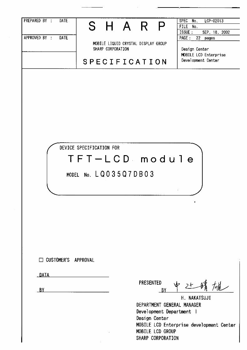
LQ035Q7DB03TFT液晶モジュール
( 形 名 : LQ035Q7DB03 )
データシート
資料 No.: LCP-02013
作成日: 2002 年 9 月 18 日
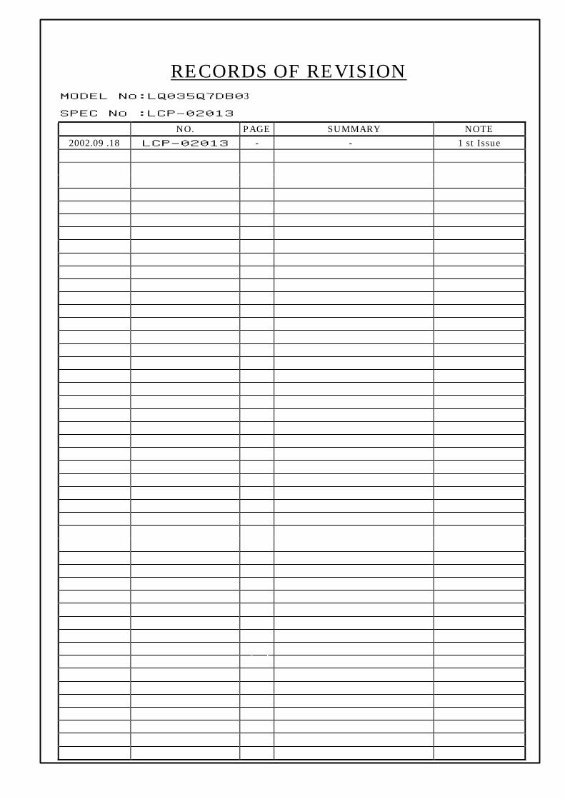
RECORDS OF REVISION MODEL No:LQ035Q7DB03
SPEC No :LCP-02013
NO. PAGE SUMMARY NOTE 2002.09 .18 LCP-02013 - - 1 st Issue

LCP-02013-1
NOTICE
This publication is the proprietary of SHARP and is copyrighted, with all rights reserved. Under the copyright
laws, no part of this publication may be reproduced or transmitted in any form or by any means, electronic or
mechanical for any purpose, in whole or in part, without the express written permission of SHARP. Express
written permission is also required before any use of this publication may be made by a third party.
The application circuit examples in this publication are provided to explain the representative applications of
SHARP's devices and are not intended to guarantee any circuit design or permit any industrial property right or
other rights to be executed. SHARP takes no responsibility for any problems related to any industrial property
right or a third party resulting from the use of SHARP's devices, except for those resulting directly from device
manufacturing processes.
In the absence of confirmation by device specification sheets, SHARP takes no responsibility for any defects that
occur in equipment using any of SHARP's devices, shown in catalogs, data books, etc. Contact SHARP in order to
obtain the latest device specification sheets before using any SHARP's device.
SHARP reserves the right to make changes in the specifications, characteristics, data, materials, structures and
other contents described herein at any time without notice in order to improve design or reliability. Contact SHARP
in order to obtain the latest specification sheets before using any SHARP's device. Manufacturing locations are also
subject to change without notice.
Observe the following points when using any device in this publication. SHARP takes no responsibility for
damage caused by improper use of the devices.
The devices in this publication are designed for use in general electronic equipment designs, such as:
・Personal computers ・Office automation ・Telecommunication equipment
・Test and measurement equipment ・Industrial control
・Audio visual and multimedia equipment ・Consumer electronics
The appropriate design measures should be taken to ensure reliability and safety when SHARP's
devices are used for equipment such as:
・Transportation control and safety equipment(i.e., aircraft, trains, automobiles, etc.)
・Traffic signals ・Gas leakage sensor breakers
・Alarm equipment ・Various safety devices etc.
SHARP's devices shall not be used for equipment that requires extremely high level of reliability,
such as:
・Military and space applications ・Nuclear power control equipment
・Medical equipment for life support
Contact a SHARP representative, in advance, when intending to use SHARP's devices for any "specific"
applications other than those recommended by SHARP.
Contact and consult with a SHARP representative if there are any questions about the contents of this
publication.
LCP-02013-2
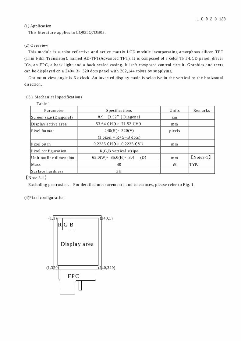
(1) Application
This literature applies to LQ035Q7DB03.
(2) Overview
This module is a color reflective and active matrix LCD module incorporating amorphous silicon TFT
(Thin Film Transistor), named AD-TFT(Advanced TFT). It is composed of a color TFT-LCD panel, driver
ICs, an FPC, a back light and a back sealed casing. It isn’t composed control circuit. Graphics and texts
can be displayed on a 240×3×320 dots panel with 262,144 colors by supplying.
Optimum view angle is 6 o’clock. An inverted display mode is selective in the vertical or the horizontal
direction.
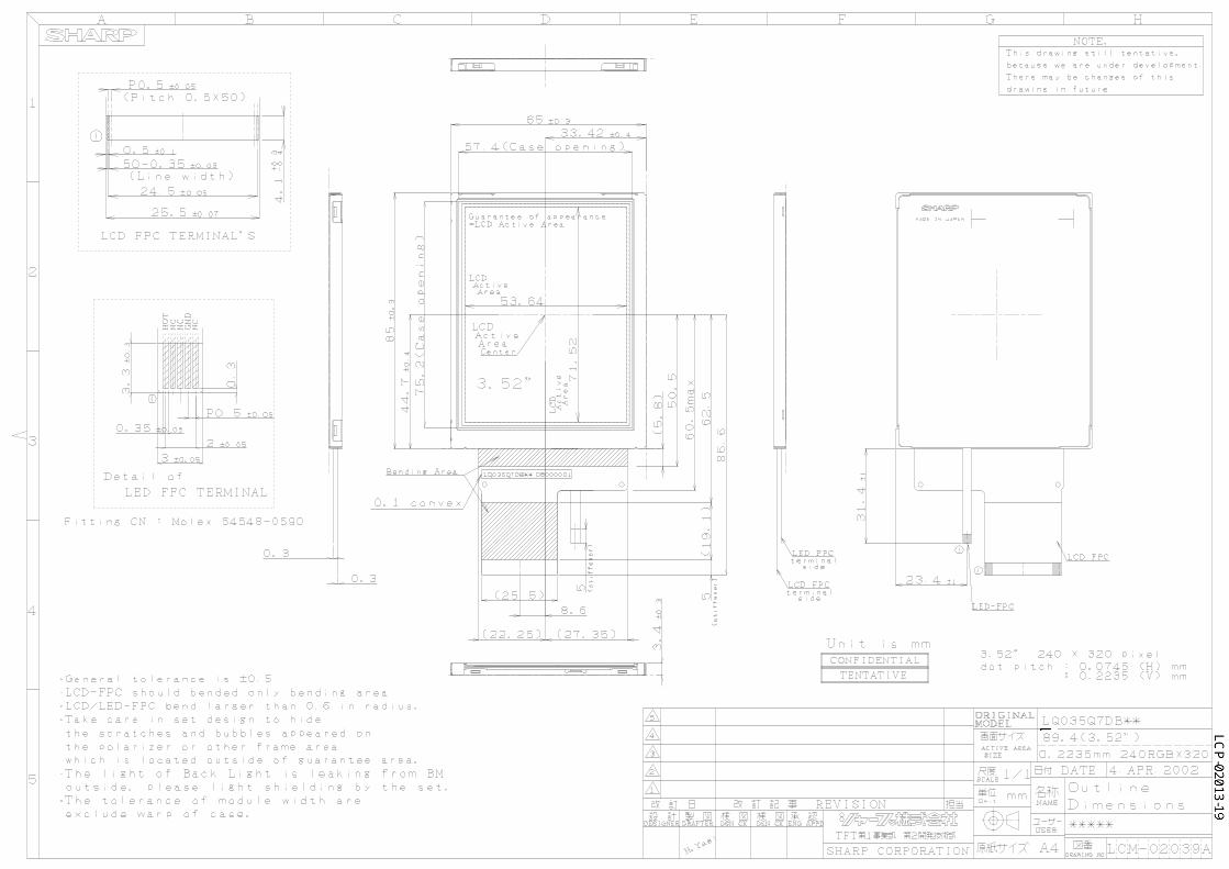
(3)Mechanical specifications
Table 1
Parameter Specifications Units Remarks
Screen size (Diagonal) 8.9 [3.52”] Diagonal cm
Display active area 53.64(H)×71.52(V) mm
Pixel format 240(H)×320(V)
(1 pixel = R+G+B dots)
pixels
Pixel pitch 0.2235(H)×0.2235(V) mm
Pixel configuration R,G,B vertical stripe
Unit outline dimension 65.0(W)×85.0(H)×3.4 (D) mm 【Note3-1】
Mass 40 g TYP.
Surface hardness 3H
【Note 3-1】
Excluding protrusion. For detailed measurements and tolerances, please refer to Fig. 1.
(4)Pixel configuration
R G B
Display area
FPC
(240,1) (1,1)
(240,320) (1,320)

LCP-02013-3
(5)Input/Output terminal
5-1)TFT-LCD panel driving section
Table2
Pin No. Symbol I/O Description Remarks
1 VDD - Power supply of gate driver(high level)
2 AGND -
3 MOD I Control signal of gate driver 【Note5-1】
4 MOD I Control signal of gate driver 【Note5-1】
5 U/L I Selection for vertical scanning direction 【Note5-2】
6 SPS I Start signal of gate driver
7 CLS I Clock signal of gate driver
8 AGND -
9 VEE - Power supply of gate driver(low level)
10 VEE - Power supply of gate driver(low level)
11 VCOM I Common electrode driving signal
12 VCOM I Common electrode driving signal
13 SPL I/O Sampling start signal
14 R0 I RED data signal(LSB)
15 R1 I RED data signal
16 R2 I RED data signal
17 R3 I RED data signal
18 R4 I RED data signal
19 R5 I RED data signal(MSB)
20 G0 I GREEN data signal(LSB)
21 G1 I GREEN data signal
22 G2 I GREEN data signal
23 G3 I GREEN data signal
24 G4 I GREEN data signal
25 G5 I GREEN data signal(MSB)
26 B0 I BLUE data signal(LSB)
27 B1 I BLUE data signal
28 B2 I BLUE data signal
29 B3 I BLUE data signal
30 B4 I BLUE data signal
31 B5 I BLUE data signal(MSB)
32 VSHD - Power supply of digital
33 DGND - Ground(digital)
34 PS I Power save signal
(Please don’t carry out use by “Low” fixation)
35 LP I Data latch signal of source driver
36 DCLK I Data sampling clock signal
37 LBR I Selection for horizontal scanning direction 【Note5-3】
38 SPR I/O Sampling start signal
39 VSHA - Power supply(analog)

LCP-02013-4
Pin No. Symbol I/O Description Remarks
40 AGND -
41 AGND -
42 REV I reverse control signal
43 COM O Produce REV signal with the amplitude of AGND-VSHA
44 AGND -
45 AGND -
46 AGND -
47 AGND -
48 AGND -
49 AGND -
50 AGND - Ground(Analog)
【Note5-1】See section(7-1)-(A) ”※Cautions when you turn on or off the power supply”.
【Note5-2】Selection for vertical scanning direction
U/L Scanning direction (Pixel configuration)
Low Normal scanning ( X , 1 )
↓
( X , 320 )
High Inverted scanning ( X , 1)
↑
( X , 320)
【Note5-3】Selection for horizontal scanning direction
LBR SPL SPR Scanning direction (Pixel configuration)
High Input Output Normal scanning (1,Y) → (240,Y)
Low Output Input Inverted scanning (1,Y) ← (240,Y)
5-2)Back light driving section
Table3
Pin No. Symbol I/O Description Remark
1 VL1 I Power supply for LED (High voltage)
2 N.C - -
3 N.C - -
4 VL2 I Power supply for LED (Low voltage)
5 N.C - -

LCP-02013-5
(6)Absolute Maximum Ratings
Table 4
Parameter Symbol Condition Ratings Unit Remark
Power supply(source/Analog) VSHA Ta=25℃ -0.3~+7.0 V
Power supply(source/Digital) VSHD Ta=25℃ -0.3~+7.0 V
Power supply (gate) VDD Ta=25℃ -0.3~+35.0 V
Power supply (gate) VDD-VEE Ta=25℃ -0.3~+35.0 V
Input voltage (Digital) VID Ta=25℃ -0.3~VSHD+0.3 V [Terminal①]
Operating temperature
(panel surface)
Topp - -10~60 ℃ 【Note6】
Storage temperature Tstg - -25~70 ℃ 【Note6-2】
[Terminal①] MOD,U/L,SPS,CLS,SPL,R0~R5,G0~G5,B0~B5,LP,DCLK,LBR,SPR,PS,REV
【Note6-2】Humidity: 95%RH Max.(at Ta ≦ 40℃). Maximum wet-bulb temperature is less than 39℃
(at Ta > 40℃). Condensation of dew must be avoided.
LCP-02013-6
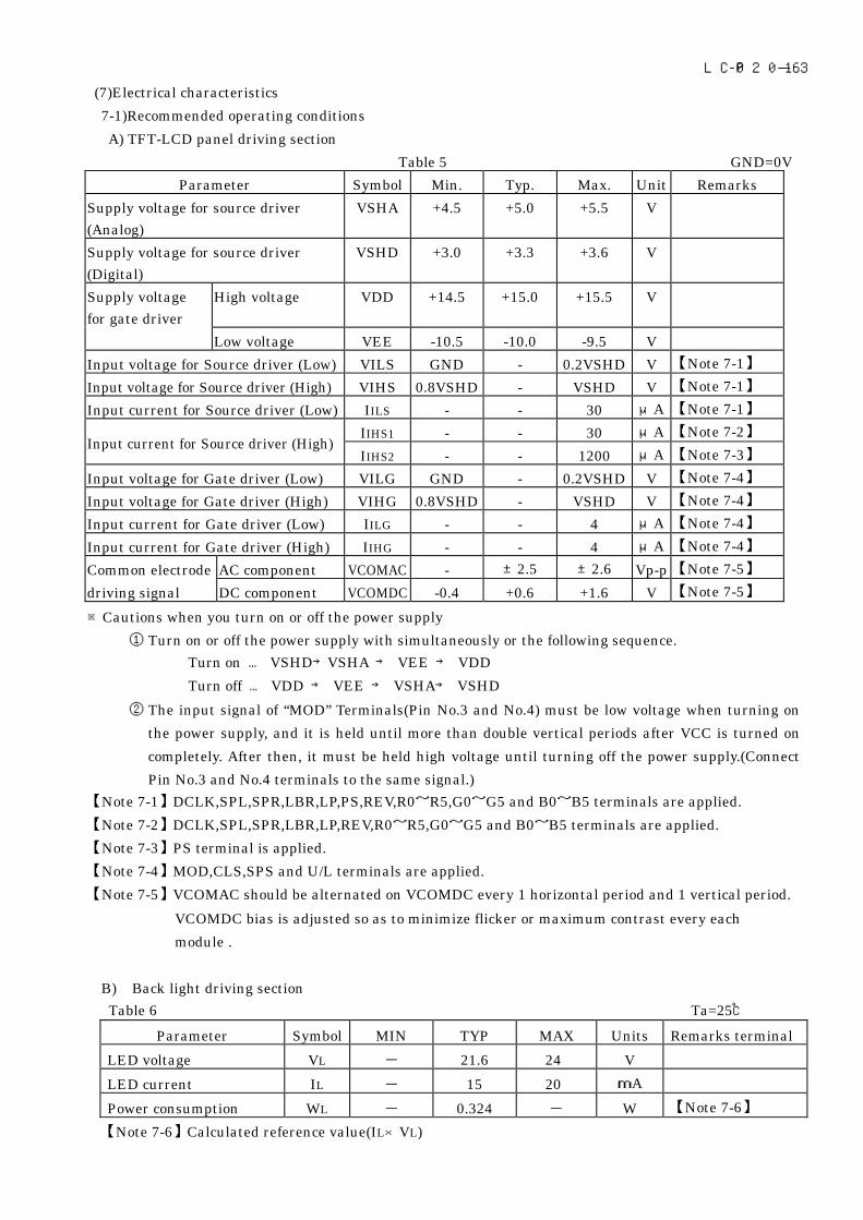
(7)Electrical characteristics
7-1)Recommended operating conditions
A) TFT-LCD panel driving section
Table 5 GND=0V
Parameter Symbol Min. Typ. Max. Unit Remarks
Supply voltage for source driver (Analog)
VSHA +4.5 +5.0 +5.5 V
Supply voltage for source driver (Digital)
VSHD +3.0 +3.3 +3.6 V
Supply voltage for gate driver
High voltage VDD +14.5 +15.0 +15.5 V
Low voltage VEE -10.5 -10.0 -9.5 V
Input voltage for Source driver (Low) VILS GND - 0.2VSHD V 【Note 7-1】
Input voltage for Source driver (High) VIHS 0.8VSHD - VSHD V 【Note 7-1】
Input current for Source driver (Low) IILS - - 30 μA 【Note 7-1】
IIHS1 - - 30 μA 【Note 7-2】 Input current for Source driver (High)
IIHS2 - - 1200 μA 【Note 7-3】
Input voltage for Gate driver (Low) VILG GND - 0.2VSHD V 【Note 7-4】
Input voltage for Gate driver (High) VIHG 0.8VSHD - VSHD V 【Note 7-4】
Input current for Gate driver (Low) IILG - - 4 μA 【Note 7-4】
Input current for Gate driver (High) IIHG - - 4 μA 【Note 7-4】
Common electrode AC component VCOMAC - ±2.5 ±2.6 Vp-p 【Note 7-5】
driving signal DC component VCOMDC -0.4 +0.6 +1.6 V 【Note 7-5】
※ Cautions when you turn on or off the power supply
① Turn on or off the power supply with simultaneously or the following sequence.
Turn on … VSHD→VSHA → VEE → VDD
Turn off … VDD → VEE → VSHA→ VSHD
② The input signal of “MOD” Terminals(Pin No.3 and No.4) must be low voltage when turning on
the power supply, and it is held until more than double vertical periods after VCC is turned on
completely. After then, it must be held high voltage until turning off the power supply.(Connect
Pin No.3 and No.4 terminals to the same signal.)
【Note 7-1】DCLK,SPL,SPR,LBR,LP,PS,REV,R0~R5,G0~G5 and B0~B5 terminals are applied.
【Note 7-2】DCLK,SPL,SPR,LBR,LP,REV,R0~R5,G0~G5 and B0~B5 terminals are applied.
【Note 7-3】PS terminal is applied.
【Note 7-4】MOD,CLS,SPS and U/L terminals are applied.
【Note 7-5】VCOMAC should be alternated on VCOMDC every 1 horizontal period and 1 vertical period.
VCOMDC bias is adjusted so as to minimize flicker or maximum contrast every each
module .
B) Back light driving section
Table 6 Ta=25℃
Parameter Symbol MIN TYP MAX Units Remarks terminal
LED voltage VL - 21.6 24 V
LED current IL - 15 20 mA
Power consumption WL - 0.324 - W 【Note 7-6】
【Note 7-6】Calculated reference value(IL×VL)
LCP-02013-7
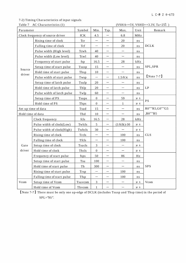
7-2) Timing Characteristics of input signals
Table 7 AC Characteristics (1) (VSHA=+5V, VSHD=+3.3V, Ta=25℃)
Parameter Symbol Min. Typ. Max. Unit Remark
Clock frequency of source driver fCK 4.5 - 6.8 MHz
Rising time of clock Tcr - - 20 ns
Falling time of clock Tcf - - 20 ns
Pulse width (High level) Tcwh 40 - - ns
Pulse width (Low level) Tcwl 40 - - ns
DCLK
Frequency of start pulse fsp 16.5 - 28 kHz
Setup time of start pulse Tsusp 15 - - ns
Hold time of start pulse Thsp 10 - - ns
Pulse width of start pulse Twsp - - 1.5/fCK ns
SPL,SPR
【Note 7-7】
Setup time of latch pulse Tsulp 20 - - ns
Hold time of latch pulse Thlp 20 - - ns LP
Pulse width of latch pulse Twlp 60 - - ns
Setup time of PS Tsups 0 - 59 μs
Source
driver
Hold time of PS Thps 0 - 1 μs PS
Set up time of data Tsud 15 - - ns
Hold time of data Thd 10 - - ns
R0~R5,G0~G5
,B0~B5
Clock frequency fcls 16.5 - 28 kHz
Pulse width of clock(Low) Twlcls 5 - (1/fclk)-30 μs
Pulse width of clock(High) Twhcls 30 - - μs
Rising time of clock Trcls - - 100 ns
Falling time of clock Tfcls - - 100 ns
Setup time of clock Tsucls 3 - - μs
Hold time of clock Thcls 0 - - μs
CLS
Frequency of start pulse fsps 50 - 86 Hz
Setup time of start pulse Tsu 100 - - ns
Hold time of start pulse Th 300 - - ns
Rising time of start pulse Trsp - - 100 ns
Gate
driver
Falling time of start pulse Tfsp - - 100 ns
SPS
Vcom Setup time of Vcom Tsuvcom 3 - - μs Vcom
Hold time of Vcom Thvcom 1 - - μs
【Note 7-7】There must be only one up-edge of DCLK (includes Tsusp and Thsp time) in the period of
SPL=”Hi”.

LCP-02013-8
Fig.(a) Horizontal timing chart
Twlp
Tsusp Thsp
(1,n) (2,n) (240,n) (1,n+1
Twlp Thlp
Tsulp
Tsud Thd
Tcwl Tcwh
Tch Tcr
80%
20%
80%
20%
80%
2 240
Twsp
Twh
Twl
DCLK
LP
SPL
R0~R5
G0~G5
B0~B5
CLS
PS
VCOM
Thcls Tsucls
Tsups Thps
Tsuvcom Thvcom
1

LCP-02013-9
Fig.(b) Vertical timing chart
1
Tsusps
Twlp Thlpck
80% CLS
SPS
2 8 9 327
Thsps
Trcls Tfcls
Trsps Tfsps
20% 20%
20%
80% 80%
20%
20%
(1~240,1) (1~240,2) (1~240,320)
1 2
Tfcls 1
Twlcls
Twhcls
20%
80%
LINE1 LINE2 LINE320
Tfsps 1
R0~R5
G0~G5
B0~B5
Non-display period Non-display period

LCP-02013-10
7-3)Power consumption
Measurement condition : SPS=60Hz,CLS=15.73kHz,SPL=15.73kHz,DCLK=6.3MHz
The term of PS=”Lo” in one horizontal period … 37μsec(234DCLK)
Ta=25℃
Table 8 when normal scan mode
Parameter Sym Conditions MIN TYP MAX Unit Remarks
Analog ISHA VSHA=+5.0V - 3.0 6.5 mA 【Note 7-8】 Source
current Digital ISHD VSHD=+3.3V - 2.0 3.5 mA 【Note 7-8】
High IDD VDD=+15.0V - 0.05 0.10 mA 【Note 7-9】 Gate
current Low IEE VEE=-10.0V - -0.05 -0.10 mA 【Note 7-9】
【Note 7-8】Vertical stripe pattern alternating 21 gray scale (GS21) with 42 gray scale (GS42) every 1 dot.
【Note 7-9】64-Gray-bar vertical pattern (GS0 ~ GS63 for horizontal way)

LCP-02013-11
(8)Input Signals, Basic Display Color and Gray Scale of Each Color
Table 9
Colors & Data signal
Gray scale Gray
Scale
R0 R1 R2 R3 R4 R5 G0 G1 G2 G3 G4 G5 B0 B1 B2 B3 B4 B5
Black - 0 0 0 0 0 0 0 0 0 0 0 0 0 0 0 0 0 0
Blue - 0 0 0 0 0 0 0 0 0 0 0 0 1 1 1 1 1 1
Green - 0 0 0 0 0 0 1 1 1 1 1 1 0 0 0 0 0 0
Cyan - 0 0 0 0 0 0 1 1 1 1 1 1 1 1 1 1 1 1
Red - 1 1 1 1 1 1 0 0 0 0 0 0 0 0 0 0 0 0
Magenta - 1 1 1 1 1 1 0 0 0 0 0 0 1 1 1 1 1 1
Yellow - 1 1 1 1 1 1 1 1 1 1 1 1 0 0 0 0 0 0
Basic color
White - 1 1 1 1 1 1 1 1 1 1 1 1 1 1 1 1 1 1
Black GS0 0 0 0 0 0 0 0 0 0 0 0 0 0 0 0 0 0 0
ñ GS1 1 0 0 0 0 0 0 0 0 0 0 0 0 0 0 0 0 0
Darker GS2 0 1 0 0 0 0 0 0 0 0 0 0 0 0 0 0 0 0
ñ â â â â
ò â â â â
Brighter GS61 1 0 1 1 1 1 0 0 0 0 0 0 0 0 0 0 0 0
ò GS62 0 1 1 1 1 1 0 0 0 0 0 0 0 0 0 0 0 0
Gray S
cale of red
Red GS63 1 1 1 1 1 1 0 0 0 0 0 0 0 0 0 0 0 0
Black GS0 0 0 0 0 0 0 0 0 0 0 0 0 0 0 0 0 0 0
ñ GS1 0 0 0 0 0 0 1 0 0 0 0 0 0 0 0 0 0 0
Darker GS2 0 0 0 0 0 0 0 1 0 0 0 0 0 0 0 0 0 0
ñ â â â â
ò â â â â
Brighter GS61 0 0 0 0 0 0 1 0 1 1 1 1 0 0 0 0 0 0
ò GS62 0 0 0 0 0 0 0 1 1 1 1 1 0 0 0 0 0 0 G
ray Scale of green
Green GS63 0 0 0 0 0 0 1 1 1 1 1 1 0 0 0 0 0 0
Black GS0 0 0 0 0 0 0 0 0 0 0 0 0 0 0 0 0 0 0
ñ GS1 0 0 0 0 0 0 0 0 0 0 0 0 1 0 0 0 0 0
Darker GS2 0 0 0 0 0 0 0 0 0 0 0 0 0 1 0 0 0 0
ñ â â â â
ò â â â â
Brighter GS61 0 0 0 0 0 0 0 0 0 0 0 0 1 0 1 1 1 1
ò GS62 0 0 0 0 0 0 0 0 0 0 0 0 0 1 1 1 1 1
Gray S
cale of bleu
Bleu GS63 0 0 0 0 0 0 0 0 0 0 0 0 1 1 1 1 1 1
0 :Low level voltage 1 :High level voltage
Each basic color can be displayed in 64 gray scales from 6 bit data signals. According to the combination of
total 18 bit data signals, the 262,144-color display can be achieved on the screen.
LCP-02013-12
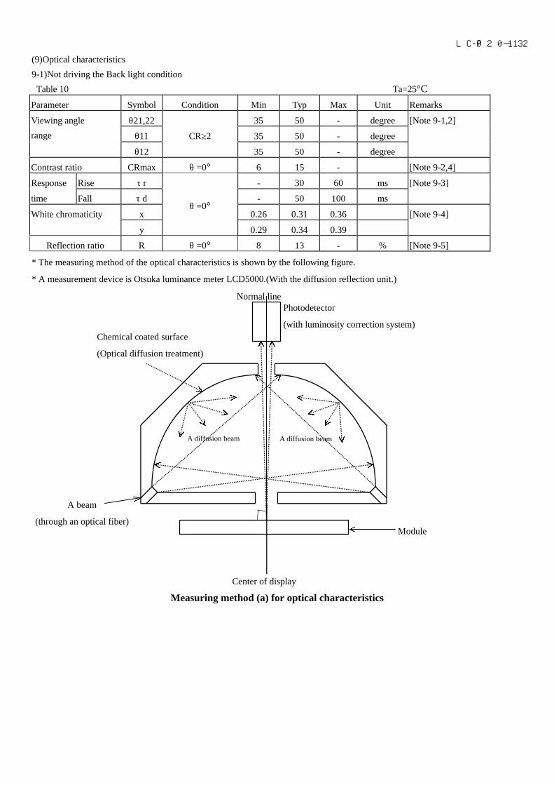
(9)Optical characteristics
9-1)Not driving the Back light condition
Table 10 Ta=25°C
Parameter Symbol Condition Min Typ Max Unit Remarks
θ21,22 35 50 - degree [Note 9-1,2]
θ11 CR≥2 35 50 - degree
Viewing angle
range
θ12 35 50 - degree
Contrast ratio CRmax θ =0° 6 15 - [Note 9-2,4]
Response Rise τ r - 30 60 ms [Note 9-3]
time Fall τ d - 50 100 ms
White chromaticity x 0.26 0.31 0.36 [Note 9-4]
y
θ =0°
0.29 0.34 0.39
Reflection ratio R θ =0° 8 13 - % [Note 9-5]
* The measuring method of the optical characteristics is shown by the following figure.
* A measurement device is Otsuka luminance meter LCD5000.(With the diffusion reflection unit.)
Center of display
Measuring method (a) for optical characteristics
Photodetector
(with luminosity correction system)
Module
Chemical coated surface
(Optical diffusion treatment)
A diffusion beam A diffusion beam
Normal line
A beam
(through an optical fiber)

LCP-02013-13
9-2)Driving the Back light condition
Table 11 Ta=25°C
Parameter Symbol Condition Min Typ Max Unit Remarks
θ21,22 30 40 - degree [Note 9-1,2,6]
θ11 CR≥2 40 50 - degree
Viewing angle
range
θ12 30 40 - degree
Contrast ratio Crmax θ = 0° 55 85 - [Note 9-2]
Response Rise τ r - 30 60 ms [Note 9-3]
time Fall τ d - 50 100 ms
White chromaticity x 0.27 0.32 0.37
y
0.29 0.34 0.39
Brightness Y θ = 0° - 55 - (cd/m2) IL=20mA
LED life time LL IL=15mA - 10000 - hour [Note 9-7]
* The measuring method of the optical characteristics is shown by the following figure.
* A measurement device is TOPCON luminance meter BM-5(A).(Viewing cone 1)
Measuring method (c) for optical characteristics
Photodetector(including luminosity facter)
Center
LCD module

LCP-02013-14
[Note 9-1] Viewing angle range is defined as follows.
6o’clock direction
θ1 2
θ2 2
θ1 1
θ2 1
Normal line
Definition for viewing angle
[Note 9-2] Definition of contrast ratio:
The contrast ratio is defined as follows:
Photodetecter output with all pixels white(GS63)
Contrast ratio(CR)=
Photodetecter output with all pixels black(GS0)
VCOMAC=5.0Vp-p
[Note 9-3] Definition of response time:
The response time is defined as the following figure and shall be measured by switching
the input signal for "black" and "white".
0%
10%
90%
100%
Black WhiteWhite
τ d τ r
Time
Photodetecter output(arbitrary unit)
LCP-02013-15
[Note 9-4] A measurement device is Minolta CM-2002.
[Note 9-5] Definition of reflection ratio
Reflection ratio =
[Note 9-6] A measurement device is ELDIM EZContrast
[Note 9-7]This is the reference vlue. The White-LED life time is defind as a time when brightness not to become
under 50% of the original value(at Ta=25℃)
(10) Display quality
The display quality of the color TFT-LCD module shall be in compliance with
the Incoming Inspection Standards for TFT-LCD..
(11)Mechanical characteristics
11-1) External appearance
See Fig. 1
11-2) FPC (for LCD panel) characteristics
(1)Specific connector
FH12A-50S-0.5SH(HIROSE)
(2) Bending endurance of the bending slits portion
No line of the FPC is broken for the bending test (Bending radius=0.6mm and
angle=90°) in 30 cycles.
Light detected level of the reflection by the LCD module
Light detected level of the reflection by the standard white board

LCP-02013-16
(12)Handling Precautions
12-1) Insertion and taking out of FPCs
Be sure insert and take out of the FPC into the connector of the set after turning off the power
supply on the set side.
12-2) Handling of FPCs
The FPC for LCD panel shall be bent only slit portion. The bending slit shall be bent uniformly
on the whole slit portion with bending radius larger than 0.6mm ,and only inner side (back side
of the module). Don’t bend it outer side (display surface side).
Don’t give the FPCs too large force, for example, hanging the module with holding FPC.
12-3) Installation of the module
On mounting the module, be sure to fix the module on the same plane. Taking care not to warp or
twist the module.
12-4)Precaution when mounting
(1) If water droplets and oil attaches to it for a long time, discoloration and staining occurs. Wipe them off
immediately.
(2) Glass is used for the TFT-LCD panel. If it is dropped or bumped against a hard object, it may be broken.
Handle it with sufficient care.
(3)As the CMOS IC is used in this module, pay attention to static electricity when handling it. Take a
measure for grounding on the human body.
12-5)Others
(1) The liquid-crystal is deteriorated by ultraviolet rays. Do not leave it in direct sunlight and strong
ultraviolet rays for many hours.
(2) If it is kept at a temperature below the rated storage temperature, it becomes coagulated and the panel
may be broken. Also, if it is kept at a temperature above the rated storage temperature, it becomes
isotropic liquid and does not return to its original state. Therefore, it is desirable to keep it at room
temperature as much as possible.
(3) If the LCD breaks, don’t put internal liquid crystal into the mouth. When the liquid crystal sticks to the
hands, feet and clothes, wash it out immediately.
(4) Wipe off water drop or finger grease immediately. Long contact with water may cause discoloration or
spots.
(5) Observe general precautions for all electronic components.
(6) VCOM must be adjusted on condition of your final product. No adjustment causes the deterioration for
display quality.
(7) Static image should not be displayed more than 5 minutes in order to prevent from occurrence of
residual image.
LCP-02013-17
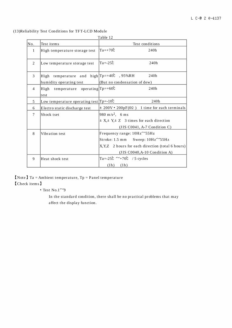
(13)Reliability Test Conditions for TFT-LCD Module
Table 12
No. Test items Test conditions
1 High temperature storage test Ta=+70℃ 240h
2 Low temperature storage test Ta=-25℃ 240h
3 High temperature and high
humidity operating test
Tp=+40℃ , 95%RH 240h
(But no condensation of dew)
4 High temperature operating
test
Tp=+60℃ 240h
5 Low temperature operating test Tp=-10℃ 240h
6 Electro static discharge test ±200V・200pF(0Ω) 1 time for each terminals
7 Shock tset 980 m/s2, 6 ms
±X,±Y,±Z 3 times for each direction
(JIS C0041, A-7 Condition C)
8 Vibration test Frequency range: 10Hz~55Hz
Stroke: 1.5 mm Sweep: 10Hz~55Hz
X,Y,Z 2 hours for each direction (total 6 hours)
(JIS C0040,A-10 Condition A)
9 Heat shock test Ta=-25℃~+70℃ / 5 cycles
(1h) (1h)
【Note】Ta = Ambient temperature, Tp = Panel temperature
【Check items】
・Test No.1~9
In the standard condition, there shall be no practical problems that may
affect the display function.
LCP-02013-18
(14) Others
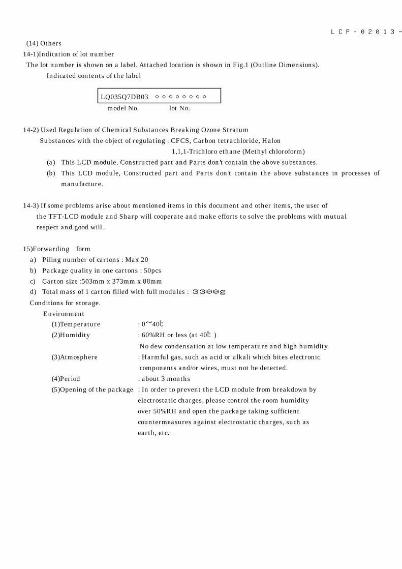
14-1)Indication of lot number
The lot number is shown on a label. Attached location is shown in Fig.1 (Outline Dimensions).
Indicated contents of the label
LQ035Q7DB03 ○○○○○○○○
model No. lot No.
14-2) Used Regulation of Chemical Substances Breaking Ozone Stratum
Substances with the object of regulating : CFCS, Carbon tetrachloride, Halon
1,1,1-Trichloro ethane (Methyl chloroform)
(a) This LCD module, Constructed part and Parts don’t contain the above substances.
(b) This LCD module, Constructed part and Parts don’t contain the above substances in processes of
manufacture.
14-3) If some problems arise about mentioned items in this document and other items, the user of
the TFT-LCD module and Sharp will cooperate and make efforts to solve the problems with mutual
respect and good will.
15)Forwarding form
a) Piling number of cartons : Max 20
b) Package quality in one cartons : 50pcs
c) Carton size :503mm x 373mm x 88mm
d) Total mass of 1 carton filled with full modules : 3300g
Conditions for storage.
Environment
(1)Temperature : 0~40℃
(2)Humidity : 60%RH or less (at 40℃)
No dew condensation at low temperature and high humidity.
(3)Atmosphere : Harmful gas, such as acid or alkali which bites electronic
components and/or wires, must not be detected.
(4)Period : about 3 months
(5)Opening of the package : In order to prevent the LCD module from breakdown by
electrostatic charges, please control the room humidity
over 50%RH and open the package taking sufficient
countermeasures against electrostatic charges, such as
earth, etc.

(おことわり)■本資料には弊社の著作権等にかかわる内容も含まれていますので、取り扱いには充分ご注意頂くと共に、本資料の内容を無断で複製しないようお願い致します。■本資料に掲載されている応用例は、弊社製品を使った代表的な応用例を説明するためのものであり、本資料によって工業所有権、その他権利の実施に対する保証または実施権の許諾を行うものではありません。また、弊社製品を使用したことにより、第三者と工業所有権等にかかわる問題が発生した場合、弊社はその責を負いません。■本資料に掲載されている製品の仕様、特性、データ、使用材料、構造などは製品改良のため予告なく変更することがあります。ご使用の際には、必ず最新の仕様書をご用命のうえ、内容のご確認をお願い致します。仕様書をご確認される事なく、万一掲載製品の使用機器等に瑕疵が生じましても、弊社はその責を負いません。■本資料に掲載されている製品のご使用に際しては、仕様書記載の絶対最大定格や使用上の注意事項等及び以下の注意点を遵守願います。なお、仕様書記載の絶対最大定格や使用上の注意事項等を逸脱した製品の使用あるいは、以下の注意点を逸脱した製品の使用に起因する損害に関して、弊社はその責を負いません。
(注意点)① 本資料に掲載されている製品は原則として下記の用途に使用する目的で製造された製品です。
・電算機 ・OA機器 ・通信機器[端末]・計測機器 ・工作機器 ・AV機器 ・家電製品
なお上記の用途であっても②または③に記載の機器に該当する場合は、それぞれ該当する注意点を遵守願います。② 機能・精度等において高い信頼性・安全性が必要とされる下記の用途に本資料に掲載されている製品を使用される場合は、これらの機器の信頼性および安全性維持のためにフェールセーフ設計や冗長設計の措置を講じる等、システム・機器全体の安全設計にご配慮頂いたうえでご使用下さい。・運送機器[航空機、列車、自動車等]の制御または各種安全装置にかかわるユニット・交通信号機 ・ガス漏れ検知遮断機 ・防災防犯装置 ・各種安全装置等③ 機能、精度等において極めて高い信頼性・安全性が必要とされる下記の用途にはご使用にならないで下さい。・宇宙機器 ・通信機器[幹線] ・原子力制御機器 ・医療機器 等④ 上記①、②、③のいずれに該当するか疑義のある場合は弊社販売窓口までご確認願います。■本資料に掲載されている製品のうち、外国為替及び外国貿易法に定める戦略物資に該当するものについては、輸出する場合、同法に基づく輸出許可・承認が必要です。■本資料に関してご不明な点がありましたら、事前に弊社販売窓口までご連絡頂きますようお願い致します。

<営業お問い合せ先>
電子部品営業本部 〒545- 8522 大阪市阿倍野区長池町22番22号 (06 )6621- 1221 (大代表)
第3統轄営業部 〒162- 8408 東京都新宿区市谷八幡町8番地 (03 )3260- 1161 (大代表)
青梅営業所 〒205- 0001 東京都羽村市五ノ神4丁目14番5号 (042 )579- 2301 (代 表)
三多摩営業所 〒191- 0003 東京都日野市日野台5丁目5番4号 (042 )581- 6092 (代 表)
大宮営業所 〒330- 0038 さいたま市宮原町2丁目107番2号 (048 )654- 8835 (代 表)
水戸営業所 〒310- 0851 水戸市千波町1963番地 (029 )243- 7600 (代 表)
仙台営業所 〒984- 0002 仙台市若林区卸町東3丁目1番27号 (022 )288- 9612 (代 表)
長野営業所 〒399- 0002 松本市芳野8番14号 (0263 )27- 1677 (代 表)
横浜営業所 〒222- 0033 横浜市港北区新横浜3丁目2番5号 (045 )478- 2580 (代 表)
大阪営業所 〒545- 8522 大阪市阿倍野区長池町22番22号 (06 )6624- 6473 (代 表)
神戸営業所 〒661- 0981 兵庫県尼崎市猪名寺3丁目2番10号 (06 )6422- 8931 (代 表)
福岡営業所 〒816- 0081 福岡市博多区井相田2丁目12番1号 (092 )582- 5245 (代 表)
名古屋営業所 〒454- 0011 名古屋市中川区山王3丁目5番5号 (052 )332- 2681 (代 表)
北陸営業所 〒921- 8801 石川県石川市野々市町字御経塚4丁目103番地 (076 )249- 6121 (代 表)