Embed Size (px)
Citation preview

Nano CMOS Technology
September 15, 2014
Hiroshi Iwai,
Tokyo Institute of Technology
@Universidad Santo Tomas in Tunja,
Colombia
1
IEEE EDS Distinguished Lecture

1. Introduction
2
4. Summary and conclusions
2. Current status of CMOS device
technologies
3. Major problems for downsizing
Outline

1. Introduction
3

• There were many inventions in the 20th century:
Airplane, Nuclear Power generation, Computer,
Space aircraft, etc
• However, everything has to be controlled by electronics
• Thus, Electronics would be
the Most important invention in the 20th century
• What is Electronics: To use electrons,
and is the Electronic Circuits

Lee De Forest
Electronic Circuits started by the
invention of vacuum tube
(Triode) in 1906
Cathode
(heated) Grid
Anode
(Positive bias)
Thermal electrons from cathode
controlled by grid bias
Same mechanism as that of transistor

First Computer Eniac: made of huge number of vacuum tubes 1946Big size, huge power, short life time filament
Today's smart phonemade of semiconductor
has much higher performance with
extremely low power consumption
dreamed of replacing vacuum tube with solid-state device
6

J.E.LILIENFELD
J. E. LILIENFELD
DEVICES FOR CONTROLLED ELECTRIC CURRENT
Filed March 28, 1928
7

Capacitor structure with notch
Electron
Semiconductor
Gate Electrode
Gate Insulator
Negative bias
Positive bias
No current
Current flows
Electric
field
8
Positive bias
Positive bias
notch
notch

Source Channel Drain
0V
N+-Si P-Si
N-Si
0V
1V
Negative
Source Channel Drain
N-Si
1VN+-Si P-Si
Surface Potential
Gate Oxd
ChannelSource
Drain
Gate electrode
S D
G
0 bias for gate Positive bias for gate
Surface
Electron flow
9
0V 1V
0V 1V
Change bias
P-type semiconductor
N-type semiconductor
Negative d
irection
Built in potential barrier
At pn junction
MOSFET Change bias

However, no one could realize MOSFET operation for more than 30 years.
Because of very bad interface property between the semiconductor and gate insulator
Even Shockley!
10
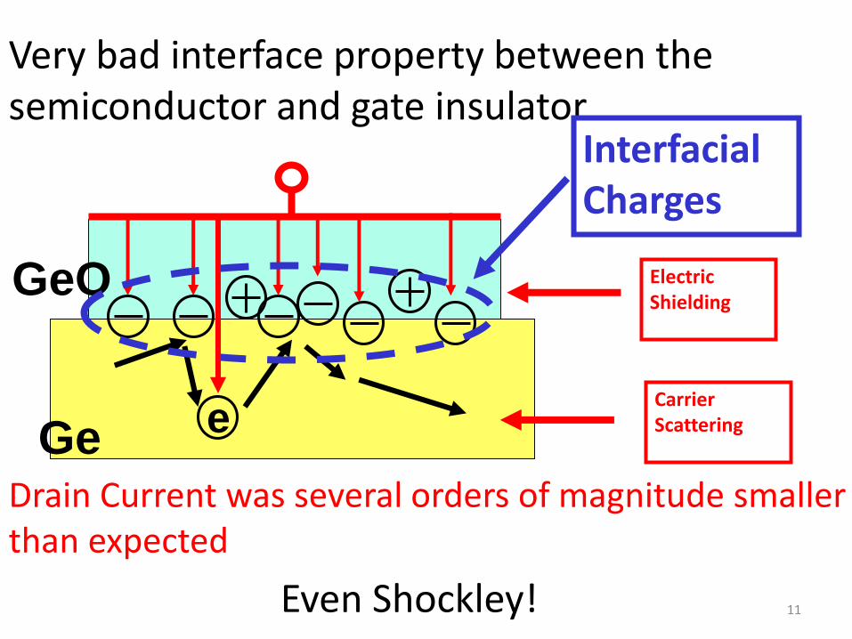
Very bad interface property between the semiconductor and gate insulator
Even Shockley!
eGe
GeO Electric Shielding
CarrierScattering
Interfacial Charges
Drain Current was several orders of magnitude smaller than expected
11
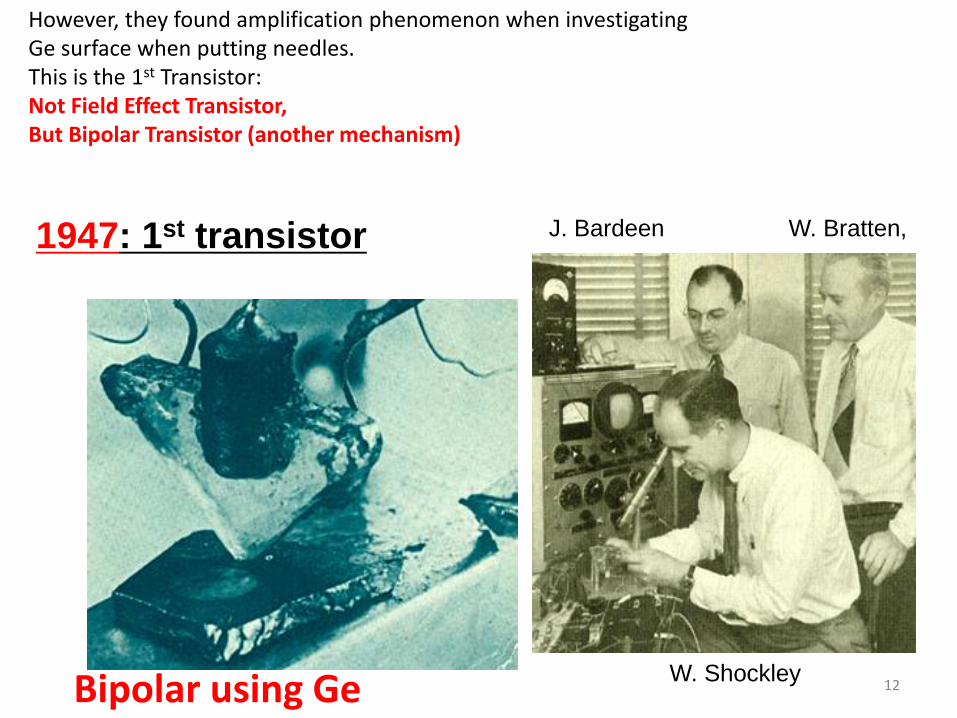
1947: 1st transistor W. Bratten,
W. ShockleyBipolar using Ge
However, they found amplification phenomenon when investigatingGe surface when putting needles.This is the 1st Transistor: Not Field Effect Transistor, But Bipolar Transistor (another mechanism)
J. Bardeen
12

1958: 1st Integrated Circuit Jack S. Kilby
Connect 2 bipolar transistors in theSame substrate by bonding wire.
13

1960: First MOSFET
by D. Kahng and M. Atalla
Al
SiO2
Si
Si/SiO2 Interface is extraordinarily good
14
Top View
Gate Oxd
ChannelSource
Drain
Gate electrodeSurface
S D
G
Electron flow

1970,71: 1st generation of LSIs (Si-MOSFETs)
1k bit DRAM Intel 1103 MPU Intel 4004(Clock 750 KHz)
15

1970 “Micro-Electronics” started.
Device: Si MOS integrated circuits
Device feature size: 10 mm
Major Appl.: Digital (Computer, PC, etc.)
Technology Revolution
because there had been no micro-electronics before(MOS IC new device, new application)
16

MOS LSI experienced continuous progress for many
years
1960s IC (Integrated Circuits) ~ 10
1970s LSI (Large Scale Integrated Circuit) ~1,000
1980s VLSI (Very Large Scale IC) ~10,000
1990s ULSI (Ultra Large Scale IC) ~1,000,000
2000s ?LSI (? Large Scale IC) ~1000,000,000
Name of Integrated Circuits Number of Transistors
17

Gate ElectrodePoly Si
Gate InsulatorSiO2
Drain
SiSubstrate
Source
Channel N-MOS (N-type MOSFET)
Gate ElectrodePoly Si
Gate InsulatorSiO2
SubstrateSi
Use Gate Field Effect for switching
ee
18

N-MOS
Source Drain
Source Drain
(N-type MOSFET)Gate
P-MOS
(P-type MOSFET)Gate
Hole flow
Electron flow
Current flow
Current flow
19

20
CMOS
Complimentary MOS
Inverter
PMOS
NMOS
When NMOS is ON, PMOS is OFF
When PMOS is ON, NMOS is OFF

21
Input Output0 V
NMOS (OFF)
PMOS (ON)
1 V
1 V
0 V
0 V
1 V (0V)
(0 V)
(-1 V)
(-1V)
S
G
D
D
B
B
G
S

22
VD
C
CVD2
1
2P =
VD
C
Q Charge Q Discharge
1 cycle Clock frequency f
fCVD2
1
2P =
CMOS: Low Power Consumption
because of no penetration between VD and earth
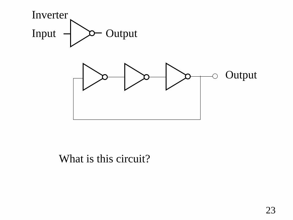
23
Output
Inverter
Input Output
What is this circuit?

24
0 1 0 1
1 0 1 0
1
0
Outputt t t
1
0
1
03t 3t
Oscillator

25
Outputt t
What is this circuit?

26
1 0 1
1 0 1
1
1
Outputt t
1 1
Latch (Memory)

AND
入力1 1 1 0 0入力2 1 0 1 0出力 1 0 0 0
NAND= NOT・AND
入力1 1 1 0 0入力2 1 0 1 0出力 0 1 1 1
1V 1V
2 input NAND circuit
Input 1
Input 1
Input 2
Input 1
Input 2
Input 2
Input 2
Input 1
Output
Output
Output
27

CMOS Technology:
Indispensible for our human society
All the human activities are controlled by CMOS
living, production, financing, telecommunication,
transportation, medical care, education,
entertainment, etc.
Without CMOS:
world economical activities immediately stop.
Cellarer phone dose not exists
Needless to say, but….
There is no computer in banks, and
28

1900 1950 1960 1970 2000
Vacuum
Tube
Transistor IC LSI VLSI
10 cm cm mm 10 mm 100 nm
In 100 years, the size reduced by one million times.
There have been many devices from stone age.
We have never experienced such a tremendous
reduction of devices in human history.
10-1m 10-2m 10-3m 10-5m 10-7m
Downsizing of the components has been the driving force for circuit evolution
2014
VLSI
14 nm
10-8m
29

Downsizing1. Reduce Capacitance
Reduce switching time of MOSFETsIncrease clock frequency
Increase circuit operation speed2. Increase number of Transistors
Parallel processingIncrease circuit operation speed
Thus, downsizing of Si devices is the most important and critical issue.30
Downsizing contribute to the performance increase
in double ways

3131
Scaling Method: by R. Dennard in 1974
1
1Wdep
1 1
I
00 V 1
X , Y , Z : K, V : K, Na : 1/K
K
K
KWdep
Wdep V/Na: K
KI
00 K
V
I : K
K=0.7 for example
Wdep: Space Charge Region
(or Depletion Region) Width
Wdep has to be suppressed
Otherwise, large leakage
between S and D
Leakage current
S D
By the scaling, Wdep is suppressed in proportion,
and thus, leakage can be suppressed.
Good scaled I-V characteristics
Potential in space charge region is
high, and thus, electrons in source are
attracted to the space charge region.

3232
Drive current
Power per chip
Integration (# of Tr)
Scaling K : K=0.7 for example
Id = vsatWgCo (Vg-Vth)
N
K-1(aK-2)K (K1 )2= a
Switching speed KK/K= K
Id per unit Wg = Id / Wg= 1
Wg (tox –1)(Vg-Vth)= Wgtox
-1(Vg-Vth)= KK-1K=Kin saturation
Co: gate C per unit area
Cg = eoeoxLgWg/tox
Id per unit Wg
Clock frequency
K
1
t
Id
K
Id/mm
f 1/K f = 1/t = 1/K
N a/K2
P a
Gate capacitance Cg K
Chip area Achip a
Lg, Wg
Tox, Vdd
Geometry &Supply voltage
K
KK/K = K
t= CgVdd/Id
a: Scaling factor
a/K2
fNCV2/2
= 1/K2 , when a=1
= 1, when a=1
Downscaling merit: Beautiful!
In the past, a>1 for most cases
3333
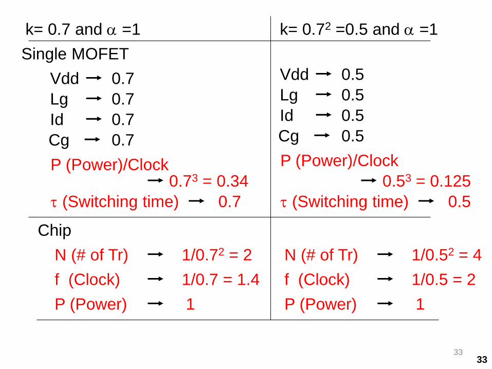
k= 0.72 =0.5 and a =1
Vdd 0.7
Single MOFET
Lg 0.7
Id 0.7
Cg 0.7
P (Power)/Clock0.73 = 0.34
t (Switching time) 0.7
Chip
N (# of Tr) 1/0.72 = 2
P (Power)
k= 0.7 and a =1
Vdd 0.5
Lg 0.5
Id 0.5
Cg 0.5
P (Power)/Clock
0.53 = 0.125
t (Switching time) 0.5
1/0.7 = 1.4f (Clock)
1
N (# of Tr) 1/0.52 = 4
P (Power)
1/0.5 = 2f (Clock)
1

3434
10 -3
10 -2
10 -1
10 0
10 1
10 2
1970 1980 1990 2000
Minimum logic Vdd (V)
Id/mm(mA/mm)
10 -3
10 -1
10 1
10 3
1970 1980 1990 2000
Id/mm
Id
1 101
10-1K (10 –2) f 1/K(10 2) 103
P a(10 1) 105
N a/K2(10 5) 104Achip a 101
Change in 30 years
Lg K 10 -2tox K(10 –2) 10-2
Vdd K(10 –2) 10-1
Idealscaling
RealChange
Idealscaling
RealChange
Idealscaling
RealChange
= faNCV2
Past 30 years scaling
N, f increaseMerit:
Demerit: P increase
Vdd scaling insufficient
Additional significantincrease in
Id, f, P
Actual past downscaling trend until year 2000
Vd scaling insufficient, a increased N, Id, f, P increased significantly
Source. Iwai and S. Ohmi, Microelectronics Reliability 42 (2002), pp.1251-1268

Late 1970’s 1mm: SCE
Early 1980’s 0.5mm: S/D resistance
Early 1980’s 0.25mm: Direct-tunneling of gate SiO2
Late 1980’s 0.1mm: ‘0.1mm brick wall’(various)
2000 50nm: ‘Red brick wall’ (various)
2000 10nm: Fundamental?
Period Expected Cause limit(size)
Many people wanted to say about the limit. Past predictions were not correct!!
35

Historically, many predictions of the limit of downsizing.
VLSI text book written 1979 predict that 0.25 micro-
meter would be the limit because of direct-tunneling current through the very thin-gate oxide.

37
C. Mead L. Conway

VLSI textbook
Finally, there appears to be a fundamentallimit 10 of approximately quarter micronchannel length, where certain physical effectssuch as the tunneling through the gateoxide ..... begin to make the devices ofsmaller dimension unworkable.
38

Potential Barrier
Wave function
Direct-tunneling effect
39
G
SD
Gate Oxide
Gate OxideGate
Electrode
Si
Substrate
Direct tunneling leakage current start to flow when the thickness is 3 nm.
Direct tunneling
current

Direct tunneling leakage was found to be OK! In 1994!
Vg = 2.0V
1.5 V
1.0 V
0.5 V
0.0 V
1.6
1.2
0.8
0.4
0.0
-0.4
0.0 0.5 1.0 1.5
Vd (V)
Vg = 2.0V
1.5 V
1.0 V
0.5 V
0.0 V
0.4
0.3
0.2
0.1
0.0
-0.1
0.0 0.5 1.0 1.5
Vd (V)
Vg = 2.0V
1.5 V
1.0 V
0.5 V
0.0 V
0.08
0.06
0.04
0.02
0.00
-0.02
0.0 0.5 1.0 1.5
Vd (V)
Vg = 2.0V
1.5 V
1.0 V
0.5 V
0.0 V
0.03
0.02
0.01
0.00
0.01
-0.4
0.0 0.5 1.0 1.5
Vd (V)
Id (
mA
/ μm)
Lg = 10 mm Lg = 5 mm Lg = 1.0 mm Lg = 0.1mm
Gate electrode
Si substrate
Gate oxide
MOSFETs with 1.5 nm gate oxide
40
G
S D
Lg

Vg = 2.0V
1.5 V
1.0 V
0.5 V
0.0 V
1.6
1.2
0.8
0.4
0.0
-0.4
0.0 0.5 1.0 1.5
Vd (V)
Vg = 2.0V
1.5 V
1.0 V
0.5 V
0.0 V
1.6
1.2
0.8
0.4
0.0
-0.4
0.0 0.5 1.0 1.5
Vd (V)
Vg = 2.0V
1.5 V
1.0 V
0.5 V
0.0 V
0.4
0.3
0.2
0.1
0.0
-0.1
0.0 0.5 1.0 1.5
Vd (V)
Vg = 2.0V
1.5 V
1.0 V
0.5 V
0.0 V
0.4
0.3
0.2
0.1
0.0
-0.1
0.0 0.5 1.0 1.5
Vd (V)
Vg = 2.0V
1.5 V
1.0 V
0.5 V
0.0 V
0.08
0.06
0.04
0.02
0.00
-0.02
0.0 0.5 1.0 1.5
Vd (V)
Vg = 2.0V
1.5 V
1.0 V
0.5 V
0.0 V
0.08
0.06
0.04
0.02
0.00
-0.02
0.0 0.5 1.0 1.5
Vd (V)
Vg = 2.0V
1.5 V
1.0 V
0.5 V
0.0 V
0.03
0.02
0.01
0.00
0.01
-0.4
0.0 0.5 1.0 1.5
Vd (V)
Id (
mA
/ μ
m)
Vg = 2.0V
1.5 V
1.0 V
0.5 V
0.0 V
0.03
0.02
0.01
0.00
0.01
-0.4
0.0 0.5 1.0 1.5
Vd (V)
Id (
mA
/ μ
m)
Lg = 10 mm Lg = 5 mm Lg = 1.0 mm Lg = 0.1mm
Gate leakage: Ig Gate Area Gate length (Lg)
Id
Drain current: Id 1/Gate length (Lg)
Lg small, Then, Ig small, Id large, Thus, Ig/Id very small
41
G
S D
Ig Id

Never Give Up!
There would be a solution!
Think, Think, and Think!
Or, Wait the time!
Some one will think for you
No one knows future!
Do not believe a text book statement, blindly!
42
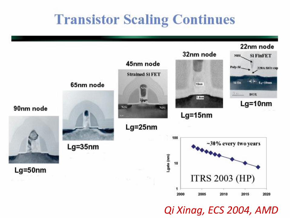
Qi Xinag, ECS 2004, AMD43

44
(1970) 10 μm 8 μm 6 μm 4 μm 3 μm 2 μm 1.2 μm
0.8 μm 0.5 μm 0.35 μm 0.25 μm 180 nm 130 nm
90 nm 65 nm 45 nm 32 nm (28 nm ) 22 nm(2012)
Feature Size / Technology Node
From 1970 to 2013 (Last year)
18 generations
Line width: 1/450
Area: 1/200,000
43 years 1 generation
2.5 years
Line width: 1/1.43 = 0.70
Area: 1/2 = 0.5
14 nm (2014)

2000 “Nano-Electronics” started.
Intel Pentium 4 : Clock 1 ~ 2 GHz
180 nm
45

2000 “Nano-Electronics” started.
Device: Still, Si CMOS integrated circuits
Device feature size: 180 nm
Major Appl.: Digital (m-processor, cell phone, etc.)
Technology Revolution??
Maybe, just evolution or innovation!
But very important so many innovations
by reducing the size!
(MOS IC, the same device, similar application)
Downsizing increases performance and
decreases the cost and power consumption.
46

5 nm gate length CMOS
H. Wakabayashi et.al, NEC
IEDM, 2003
Length of 18 Si atoms
Is a Real Nano Device!!
5 nm
47

Now, 2014 “Nano-Electronics” continued.
Device: Still, Si CMOS integrated circuits
Device feature size: a few 10 nm
Major Appl.: Still Digital (m-processor, cell phone, etc.)
Still evolution and innovation are going on.
Broadwell SoC (Intel)
http://download.intel.com/newsroom/kits/14nm/pdfs/Intel_14nm_New_uArch.pdf
48

Downsizing
Important for
- Decreasing cost, and power consumption
- Increasing performance
This is true still for today’s 14 nm !49

http://download.intel.com/newsroom/kits/14nm/pdfs/
Intel_14nm_New_uArch.pdf
Merit for downsizing to 14 nm
(Intel case)
Merit for cost, power consumption,
and performance
50

Most Recent SD Card
128GB (Bite)
= 128G X 8bit
= 1T(Tera)bit
1T = 1012 = 1Trillion
Brain Cell:10~100 Billion
World Population:7 Billion
Stars in Galaxy:100 Billion
In 2012
51

Most Recent SD Card
256GB (Bite)
= 256G X 8bit
= 2T(Tera)bit
2T = 1012 = 2Trillion
Brain Cell:10~100 Billion
World Population:7 Billion
Stars in Galaxy:100 Billion
In 2014
52

2.4cm X 3.2cm X 0.21cm
Volume:1. 6cm³ Weight:2g
Voltage:2.7 - 3.6V
Old Vacuum Tube:5cm X 5cm X 10cm, 100g, 50W
128 GB = 1Tbit
What are volume, weight, power
consumption for 1Tbit
53

Old Vacuum Tube:5cm X 5cm X 10cm
1Tbit = 10,000 X 10,000 X 10,000 bit
Volume = (5cm X 10,000) X (5cm X 10,000)
X (10cm X 10,000)
= 0.5km X 0.5km X 1km
500 m
1,0
00
m
1Tbit
Burji Khalifa
Dubai, UAE
(Year 2010)
828 m
Indian Tower
Mumbai, India
(Year 2016)
70
0 m
700 m
Pingan Intenational
Finance Center
Shanghai, China
(Year 2016)
54
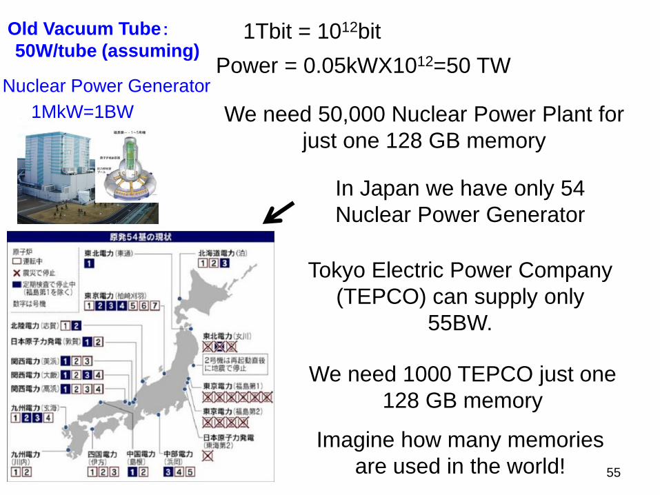
Old Vacuum Tube:50W/tube (assuming)
1Tbit = 1012bit
Power = 0.05kWX1012=50 TWNuclear Power Generator
1MkW=1BW We need 50,000 Nuclear Power Plant for
just one 128 GB memory
In Japan we have only 54
Nuclear Power Generator
Tokyo Electric Power Company
(TEPCO) can supply only
55BW.
We need 1000 TEPCO just one
128 GB memory
Imagine how many memories
are used in the world! 55

So progress of integrated
circuits by downsizing is
extremely important for
power saving.
56

Brain: Integrated Circuits
Hands, Legs:Power device
Stomach:PV device
Ear, Eye:Sensor
Mouth:RF/Opto device
57
Various semiconductor devices
Brain is very important

58
Near future smart-society has to treat huge
data.
Demand to high-performance and low power
CMOS become much more stronger.
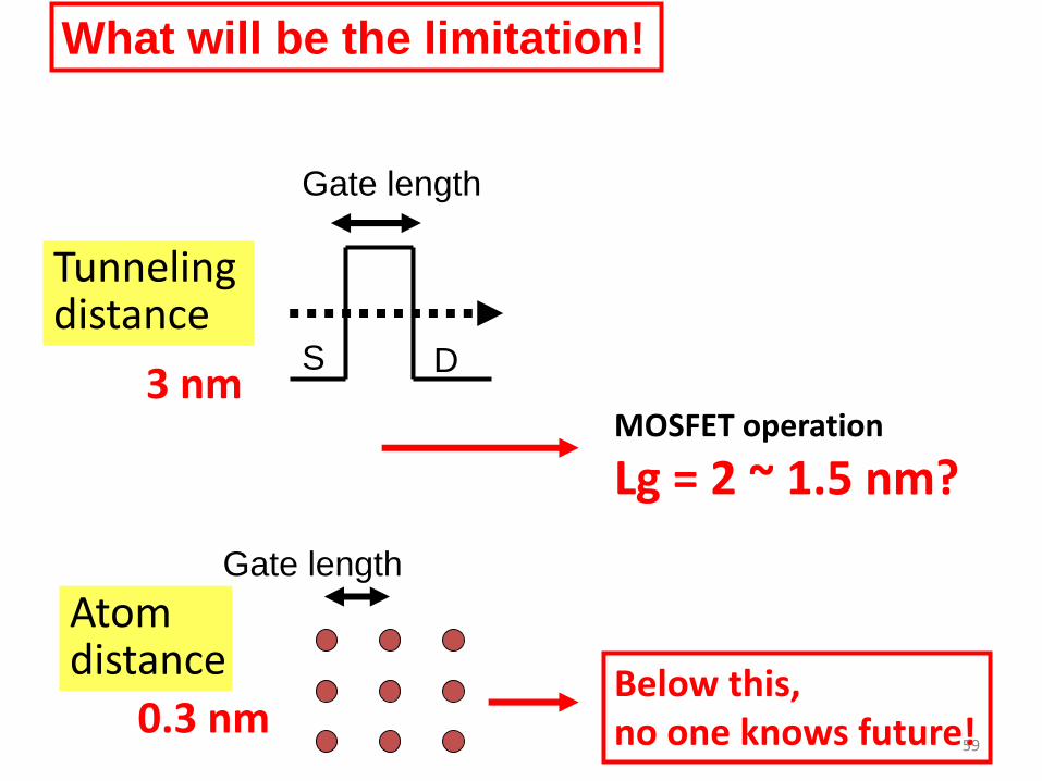
Tunnelingdistance
3 nm
Atomdistance
0.3 nm
MOSFET operation
Lg = 2 ~ 1.5 nm?
Below this, no one knows future!
What will be the limitation!
59
Gate length
Gate length
S D

By Robert Chau, IWGI 2003
0.8 nm Gate Oxide Thickness MOSFETs operates!!
0.8 nm: Distance of 3 Si atoms!!
60

So, we are now in the limitation of downsizing?
Do you believe this or do not?
61

There is a solution!To use high-k dielectrics
Thin gate SiO2Thick gate high-k dielectrics
Almost the same electric characteristics
However, very difficult and big challenge!
Remember MOSFET had not been realized without Si/SiO2!
K: Dielectric Constant
Thick
Small leakageCurrent
62

R. Hauser, IEDM Short Course, 1999Hubbard and Schlom, J Mater Res 11 2757 (1996)
●
● Gas or liquid
at 1000 K
●H
○Radio activeHe
● ● ● ● ● ●Li BeB C N O F Ne
① ● ● ● ●Na
Mg Al Si P S Cl Ar
② ① ① ① ① ① ① ① ① ① ① ● ● ● ●K Ca Sc Ti V Cr Mn Fc Co Ni Cu Zn Ga Ge As Se Br Kr
● ① ① ① ① ① ● ① ① ① ① ① ● ●Rh Sr Y Zr Nb Mo Tc Ru Rb Pd Ag Cd In Sn Sb Te I Xe● ③ ① ① ① ① ① ● ● ● ● ① ① ○ ○ ○Cs Ba
★ HfTa W Re Os Ir Pt Au Hg Tl Pb Bi Po At Rn
○ ○ ○ ○ ○ ○ ○ ○Fr Ra ☆ Rf Ha Sg Ns Hs Mt
○La Ce Pr Nd Pm Sm Eu Gd Tb Dy Ho Er Tm Yb Lu○ ○ ○ ○ ○ ○ ○ ○ ○ ○ ○ ○ ○ ○ ○Ac Th Pa U Np Pu Am Cm Bk Cf Es Fm Md No Lr
★
☆
Candidates
● ●Na Al Si P S Cl Ar
② ① ① ① ① ① ① ① ① ① ● ● ● ●K Sc Ti V Cr Mn Fc Co Ni Cu Zn Ga Ge As Se Br Kr
● ① ① ① ① ① ● ① ①
○ ○ ○ ○ ○ ○Ac Th Pa U Np Pu Am Cm Bk Cf Es Fm Md No Lr
★
☆
②
③
Unstable at Si interfaceSi + MOX M + SiO2①
Si + MOX MSiX + SiO2
Si + MOX M + MSiXOY
Choice of High-k elements for oxide
HfO2 based dielectrics
are selected as the
first generation
materials, because of
their merit in
1) band-offset,
2) dielectric constant
3) thermal stability
La2O3 based
dielectrics are
thought to be the next
generation materials,
which may not need a
thicker interfacial
layer
63

0 10 20 30 40 50
Dielectric Constant
4
2
0
-2
-4
-6
SiO2
Ba
nd
Dis
co
nti
nu
ity [
eV
]Si
XPS measurement by Prof. T. Hattori, INFOS 2003
Conduction band offset vs. Dielectric Constant
Band offset
Oxide
Leakage Current by Tunneling
64

65
PMOS
High-k gate insulator MOSFETs for Intel: EOT=1nm
EOT: Equivalent Oxide Thickness
2. Current status of CMOS
device technologies
66

More Moore to More More Moore
65nm 45nm 32nm
Technology node
M. Bohr, pp.1, IEDM2011 (Intel)
P. Packan, pp.659, IEDM2009 (Intel)
C. Auth et al., pp.131, VLSI2012 (Intel)
T. B. Hook, pp.115, IEDM2011 (IBM)
S. Bangsaruntip et al., pp.297, IEDM2009 (IBM)
Lg 35nm Lg 30nm
Main stream
(Fin,Tri, Nanowire)
22nm14nm 10nm, 7nm, 5nm, 3.5nm
Alternative
Alternative (III-V/Ge)
Channel FinFET
Emerging
Devices
Tri-Gate
Now Future
Si channel
Si
Others
(FDSOI)
Planar
Si is still main stream for future !! FD: Fully Depleted
67

Planar Fin Nanowire
Source Drain
Gate
Wdep
1
Leakage current
S D
Planar FETFin FET
Nanowire FET
Because of off-leakage control,

High-k gate dielectrics
Continued research
and development
SiO2 IL (Interfacial Layer)
is used at Si interface to
realize good mobility
Technology for direct contact of
high-k and Si is necessary
Remote SiO2-IL
scavenging
HfO2 (IBM)
EOT=0.52 nm
Si
La-silicate
MG
Direct contact with La-silicate (Tokyo.Tech)
T. Ando, et al., p.423, IEDM2009, (IBM)
T. Kawanago, et al., T-ED, vol. 59, no.
2, p. 269, 2012 (Tokyo Tech.)
K. Mistry, et al., p.247, IEDM 2007, (Intel)
TiN
HfO2
Si
SiO2
EOT=0.9nm
HfO2/SiO2
(IBM)
T.C. Chen, et al., p.8, VLSI 2009, (IBM)
Hf-based oxides
45nm
EOT:1nm
32nm
EOT:0.95nm
22nm
EOT:0.9nm
10nm, 7nm, 5nm, 3.5nm,
K. Kakushima, et al., p.8, IWDTF 2008,
(Tokyo Tech.)
EOT=0.37nm EOT=0.40nm EOT=0.48nm
0.48 → 0.37nm Increase of Id at 30%
14nm
EOT:0.?nm
69

High-k is very important, however very difficult.
70
Thickness (EOT) decreased only 0.05 nm (or 0.5 Å, or 1 atom layer) for every generation.

<80
56/9
2.05/1.5
1.1
~0.5
-
HfZrO2
22/30
(nFET/pFET)
GAA NW
STMicro.
(VLSI2008)
85
65/105
0.83/0.95
1
0.3~0.4
1.5
Hf-based
35/25
(nFET/pFET)
GAA NW
IBM
(IEDM2009)
Intel
(IEDM2007, 2009)
Intel
(VLSI2012)
Toshiba
(VLSI2012)
IBM
(IEDM2012)
Samsung
(IEDM2012)
Tokyo Tech
(ESSDERC2010)
StructureBulk Planar Tri-Gate
22nmTri-Gate NW ETSOI Bulk Planar -gate NW
45nm 32nm
Lg (nm) 35 30 30 14 22 20 65
Gate
DielectricsHf-based Hf-based SiO2 HfO2 HfO2 ? SiO2
EOT (nm) 1 0.95 0.9 3 ~1 - 3
Vth (V) ~0.4 ~0.3 ~0.2 -0.15 (nFET) 0.3~0.4 ~0.3 -0.2 (nFET)
VDD (V) 1 1 0.8 1 0.9 0.9 1
ION (mA/um)
nFET/pFET1.36/1.07 1.53/1.23 1.26/1.1 0.83 (nFET) 0.59/0.62 (Ieff) 1.2/1.05 1.32 (nFET)
DIBL
(mV/V)
nFET/pFET
~150 ~200 46/50 <50 - 104/115 62
SS
(mV/dec)- ~100 ~70 <80 - 87 70<80
56/9
2.05/1.5
1.1
~0.5
-
HfZrO2
22/30
(nFET/pFET)
GAA NW
STMicro.
(VLSI2008)
85
65/105
0.83/0.95
1
0.3~0.4
1.5
Hf-based
35/25
(nFET/pFET)
GAA NW
IBM
(IEDM2009)
Intel
(IEDM2007, 2009)
Intel
(VLSI2012)
Toshiba
(VLSI2012)
IBM
(IEDM2012)
Samsung
(IEDM2012)
Tokyo Tech
(ESSDERC2010)
StructureBulk Planar Tri-Gate
22nmTri-Gate NW ETSOI Bulk Planar -gate NW
45nm 32nm
Lg (nm) 35 30 30 14 22 20 65
Gate
DielectricsHf-based Hf-based SiO2 HfO2 HfO2 ? SiO2
EOT (nm) 1 0.95 0.9 3 ~1 - 3
Vth (V) ~0.4 ~0.3 ~0.2 -0.15 (nFET) 0.3~0.4 ~0.3 -0.2 (nFET)
VDD (V) 1 1 0.8 1 0.9 0.9 1
ION (mA/um)
nFET/pFET1.36/1.07 1.53/1.23 1.26/1.1 0.83 (nFET) 0.59/0.62 (Ieff) 1.2/1.05 1.32 (nFET)
DIBL
(mV/V)
nFET/pFET
~150 ~200 46/50 <50 - 104/115 62
SS
(mV/dec)- ~100 ~70 <80 - 87 70
Benchmark of device characteristics
71

[1] C. Auth et al., pp.131, VLSI2012 (Intel).[2] K. Mistry et al., pp.247, IEDM2007 (Intel).[3] H.-J. Cho et al., pp.350, IEDM2011 (Samsung).[4] S. Saitoh et al., pp.11, VLSI2012 (Toshiba).[5] S. Bangsaruntip et al., pp.297, IEDM2009 (IBM).
[6] T. Yamashita et al., pp.14, VLSI2011 (IBM).[7] A. Khakifirooz et al., pp.117, VLSI2012 (IBM).
ION and IOFF benchmark until 2012
[8] G. Bidal et al., pp.240, VLSI2009 (STMicroelectronics).[9] S. Sato et al., pp.361, ESSDERC2010 (Tokyo Tech.)[10] K. Cheng et al., pp.419, IEDM2012 (IBM)
1
10
100
1000
10000
0.6 0.8 1 1.2 1.4 1.6 1.8 2 2.2
ION [mA/mm]
I OF
F[n
A/m
m]
NMOS
Intel [1]
Bulk 32nm
VDD=0.8V
Intel [1]
Tri-Gate 22nm
VDD=0.8V
Intel [2]
Bulk 45nm
VDD=1V
Toshiba [4]
Tri-Gate NW
VDD=1V
Samsung [3]
Bulk 20nm
VDD=0.9V
IBM [5]
GAA NW
VDD=1V
IBM [6]
FinFET 25nm
VDD=1V
IBM [7]
ETSOI
VDD=0.9V
IBM [7]
ETSOI
VDD=1V
STMicro. [8]
GAA NW
VDD=0.9V
STMicro. [8]
GAA NW
VDD=1.1V
Tokyo Tech. [9]
-gate NW
VDD=1VIBM [10]
ETSOI
VDD=0.9V
Ieff
1
10
100
1000
10000
0.6 0.7 0.8 0.9 1 1.1 1.2 1.3 1.4 1.5 1.6
ION [mA/mm]
I OF
F[n
A/m
m]
PMOS
Intel [1]
Bulk 32nm
VDD=0.8V
Intel [1]
Tri-Gate 22nm
VDD=0.8V
Intel [2]
Bulk 45nm
VDD=1V
IBM [7]
ETSOI
VDD=1VSamsung [3]
Bulk 20nm
VDD=0.9V
IBM [5]
GAA NW
VDD=1V
IBM [6]
FinFET 25nm
VDD=1V
IBM [7]
ETSOI
VDD=0.9V
STMicro. [8]
GAA NW
VDD=1.1V
IBM [10]
ETSOI
VDD=0.9V
Ieff
Supply voltage affects significantly!
72

ION and IOFF benchmark updating
1
10
100
1000
10000
0.6 0.8 1 1.2 1.4 1.6 1.8 2 2.2
NMOS
ION [mA/mm]
I OF
F[n
A/m
m]
Intel [1]
Tri-Gate 22nm
VDD=0.8V
Toshiba [4]
Tri-Gate NW
VDD=1V
ST [2]
ETSOI 14nm
VDD=0.75V
IBM [3]
GAA NW
VDD=1V
IBM [6]
FinFET 25nm
VDD=1V
IBM [7]
ETSOI
VDD=0.9V
IBM [7]
ETSOI
VDD=1V
STMicro. [8]
GAA NW
VDD=0.9V
STMicro. [8]
GAA NW
VDD=1.1V
Tokyo Tech. [9]
-gate NW
VDD=1V
[1] C. Auth et al., pp.131, VLSI2012 (Intel).[2] Q. Liu et al., pp.228, IEDM2013 (ST).[3] S. Bangsaruntip et al., pp.526, IEDM2013 (IBM).[4] S. Saitoh et al., pp.11, VLSI2012 (Toshiba).[5] S. Bangsaruntip et al., pp.297, IEDM2009 (IBM).
[6] T. Yamashita et al., pp.14, VLSI2011 (IBM).[7] A. Khakifirooz et al., pp.117, VLSI2012 (IBM).[8] G. Bidal et al., pp.240, VLSI2009 (STMicroelectronics).[9] S. Sato et al., pp.361, ESSDERC2010 (Tokyo Tech.)
1
10
100
1000
10000
0.6 0.7 0.8 0.9 1 1.1 1.2 1.3 1.4 1.5 1.6
ION [mA/mm]
I OF
F[n
A/m
m]
PMOS
Intel [1]
Tri-Gate 22nm
VDD=0.8V
IBM [7]
ETSOI
VDD=1V
IBM [5]
GAA NW
VDD=1V
IBM [6]
FinFET 25nm
VDD=1V
IBM [7]
ETSOI
VDD=0.9V
STMicro. [8]
GAA NW
VDD=1.1V
ST [2]
ETSOI 14nm
VDD=0.75V
Lower supply voltage degrades the ratio.
73

Examples of the state of the art
Current status of Si-CMOS device
technologies
Fin, Tri gate FET
74

Fin Tri-gate
(Variation)
-gate All-around
G G G
G
G
Multi-gate structures
75
G
Tri-gate

How far can we go for production?
76
Now, Ion/Ioff ratio is typically 106.
However, it degrades significantly with decrease in Vsupply.
Rather than Ioff value, Ion/Ioff ratio is important.

[a] C. Auth et al., pp.131, VLSI2012 (Intel).[b] K. Mistry et al., pp.247, IEDM2007 (Intel).[c] H.-J. Cho et al., pp.350, IEDM2011 (Samsung).[d] S. Saitoh et al., pp.11, VLSI2012 (Toshiba).[e] S. Bangsaruntip et al., pp.297, IEDM2009 (IBM).
[f] T. Yamashita et al., pp.14, VLSI2011 (IBM).[g] A. Khakifirooz et al., pp.117, VLSI2012 (IBM).
ION and IOFF benchmark
[h] G. Bidal et al., pp.240, VLSI2009 (STMicroelectronics).[i] S. Sato et al., pp.361, ESSDERC2010 (Tokyo Tech.)[j] K. Cheng et al., pp.419, IEDM2012 (IBM)
1
10
100
1000
10000
0.6 0.8 1 1.2 1.4 1.6 1.8 2 2.2
ION [mA/mm]
I OF
F[n
A/m
m]
NMOS
Intel [a]
Bulk 32nm
VDD=0.8V
Intel [a]
Tri-Gate 22nm
VDD=0.8V
Intel [b]
Bulk 45nm
VDD=1V
Toshiba [d]
Tri-Gate NW
VDD=1V
Samsung [c]
Bulk 20nm
VDD=0.9V
IBM [5]
GAA NW
VDD=1V
IBM [g]
FinFET 25nm
VDD=1V
IBM [g]
ETSOI
VDD=0.9V
IBM [g]
ETSOI
VDD=1V
STMicro. [h]
GAA NW
VDD=0.9V
STMicro. [h]
GAA NW
VDD=1.1V
Tokyo Tech. [i]
-gate NW
VDD=1VIBM [j]
ETSOI
VDD=0.9V
Ieff
1
10
100
1000
10000
0.6 0.7 0.8 0.9 1 1.1 1.2 1.3 1.4 1.5 1.6
ION [mA/mm]
I OF
F[n
A/m
m]
PMOS
Intel [a]
Bulk 32nm
VDD=0.8V
Intel [a]
Tri-Gate 22nm
VDD=0.8V
Intel [b]
Bulk 45nm
VDD=1V
IBM [g]
ETSOI
VDD=1VSamsung [c]
Bulk 20nm
VDD=0.9V
IBM [e]
GAA NW
VDD=1V
IBM [f]
FinFET 25nm
VDD=1V
IBM [g]
ETSOI
VDD=0.9V
STMicro. [h]
GAA NW
VDD=1.1V
IBM [j]
ETSOI
VDD=0.9V
Ieff
77

HP MP SP
TOX,E (nm) 0.9 0.9 0.9
LGATE (nm) 30 34 34
IOFF (nA/um) 20-100 5-20 1-5
Tri-gate has been implemented
since 22nm node, enabling
further scaling
C. Auth et al., pp.131, VLSI2012 (Intel)
22 nm Tri-gate (Intel)
78

PMOS channel
under the gate
S/D region showing
the SiGe epitaxy
A fin width of 8nm to balance SCE and Rext
A fin height of 34nm to balance
drive current vs. capacitance
C. Auth et al., pp.131, VLSI2012 (Intel)
22 nmTri-gate (Intel)
Intel’s fin is triangle shape!
79

C.-H. Jan et al ., pp.44, IEDM2012 (Intel)
22 nmTri-gate (Intel)
・SS of 71 and 72 mV/dec for HP NMOS and PMOS, respectively
・DIBL of 30 and 35 mV/V for NMOS and PMOS, respectively
・Vth of 22 nm is about 0.1 ~0.2 V lower than that of 32nm
Very good Vth control!
80

Low Vccmin16nm node FinFETs (TSMC)S. Wu et al., pp.224, IEDM2013 (TSMC)
Low leakage (SVt : purple)
- Lg = 34 nm
- SS < 65 mV/dec.
- DIBL < 30 mV/V
- Idsat = 520/525 uA/um at 0.75 V
- Ioff = 30 pA/um
Fin patterning and formation on bulk
with 48 nm fin pitch (pitch-splitting
technique)
Poly-silicon deposition and gate
patterning with (gate pitch of 90 nm)
High-k/Metal gate RPG process
Raised source/drain with dual epitaxy
Static noise margin of 0.07 um2 high
density SRAM cell at 0.8 V and 0.6 V
81
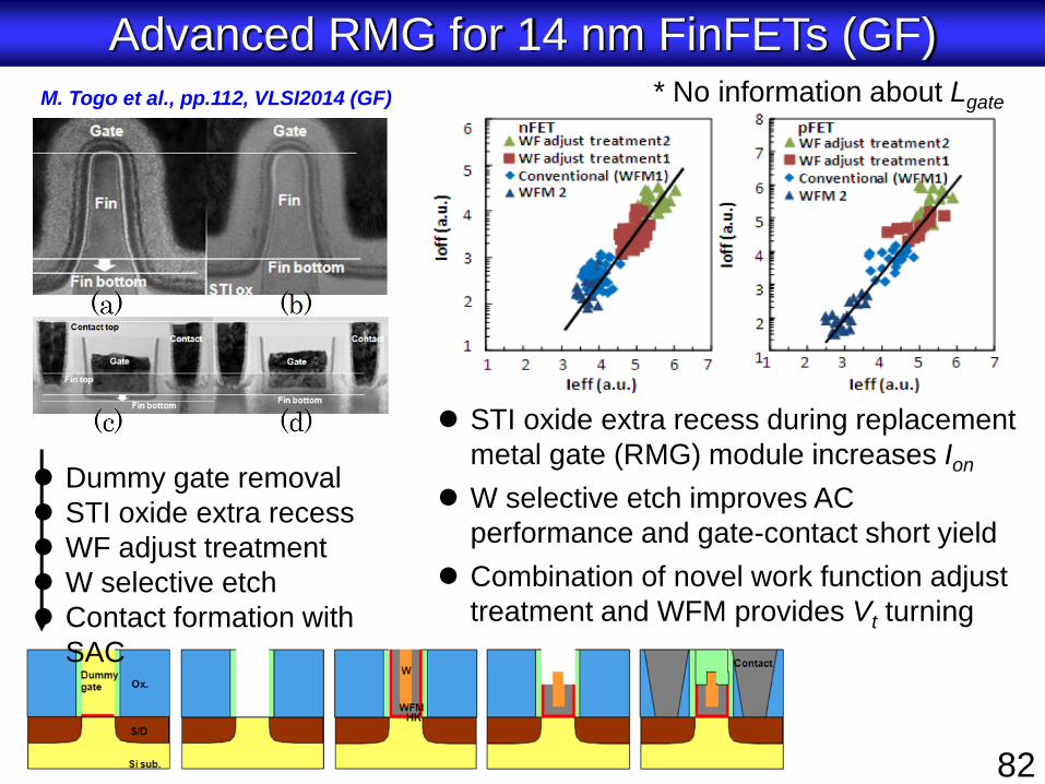
Advanced RMG for 14 nm FinFETs (GF)
M. Togo et al., pp.112, VLSI2014 (GF)
Dummy gate removal
STI oxide extra recess
WF adjust treatment
W selective etch
Contact formation with
SAC
STI oxide extra recess during replacement
metal gate (RMG) module increases Ion
W selective etch improves AC
performance and gate-contact short yield
Combination of novel work function adjust
treatment and WFM provides Vt turning
82
* No information about Lgate

http://download.intel.com/newsroom/kits/14nm/pdfs/Intel_14nm_New_uArch.pdf
Interconnects
SRAM Cell
Intel 14nm Technology by Mark Bohr, August 11. 2014
83
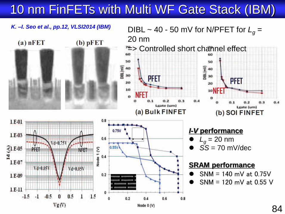
10 nm FinFETs with Multi WF Gate Stack (IBM)
K. –I. Seo et al., pp.12, VLSI2014 (IBM)
I-V performance
Lg = 20 nm
SS = 70 mV/dec
SRAM performance
SNM = 140 mV at 0.75V SNM = 120 mV at 0.55 V
DIBL ~ 40 - 50 mV for N/PFET for Lg =
20 nm
=> Controlled short channel effect
84

Examples of the state of the art
Si-CMOS device technologies
FD SOI FET
85

Dual STI for Multi-Vt at 20 nm Node (CEA-LETI)
L. Grenouillet et al., pp.64, IEDM2012 (CEA-LETI)
Wider back bias (BB)
tunability with dual STI
(shallow & deep)
Successive performance
boost and leakage current
control by BB 86

Extremely Thin SOI (ETSOI) (IBM)
・Hybrid CMOS
Si Channel nFET
Strained SiGe Channel pFET
・RO delay improvement over
FinFET with FO = 2
K. Cheng et al., pp.419, IEDM2012 (IBM)
Also, ET-SOI works very good!
87

Material Selection and RSD for 14 nm FDSOI (ST)
Q. Liu et al., pp.228, IEDM2013 (STMicroelectronics)
nMOS => Si channel/SiC RSD
pMOS => SiGe channel/SiGe RSD
88

14 nm FDSOI Technology (STMicroelectronics)
O. Weber et al., pp.14, VLSI2014 (STMicroelectronics)
New Front-End process elements
Dual SOI/SiGeOI N/P channel
Dual workfunction gate-first HKMG integration
scheme
Dual in-situ doped Si:CP/SiGeB N/P RSD
30% speed boost at the same power
55% power reduction at the same speed
over the 28nm node
89

Silicon-on-Thin-Buried Oxide CMOS (LEAP)S. Kamohara et al., pp.154, VLSI2014 (LEAP)
Very small Vth and Ion variability was
demonstrated for one million transistors.
High performance due to less S/D doping and
back bias controlling.
Confirmed 6-T SRAM operation (2 Mbit) at less
than 0.4 V with a 5.5-ps access time.
Demonstrated that the minimum operating
voltage can be controlled at <0.4 V by back-
bias against temperature variation.
90

Strain Engineered Extremely Thin SOI (IBM)
A. Khakifirooz et al., pp.117, VLSI2012 (IBM)
nFET - Strained SOI (SSDOI)
pFET – SiGe-on-insulator (SGOI)
t ~ 6 nm
Channel
91

Examples of the state of the art
Current status of Si-CMOS device
technologies
Nanowire FET
92

Fin Tri-gate
(Variation)
-gate All-around
G G G
G
G
Multi-gate structures
93
G
Tri-gate

S. Bangsaruntip et al., pp.297, IEDM2009 (IBM)
・Lg = 25~35nm GAA NW
・Hydrogen anneal provide
smooth channel surface
・Competitive with conventional
CMOS technologies
・Scaling the dimensions of NW
leads to suppressed SCE
Gate All Around Nanowire (GAA NW) (IBM)
94

G. Bidal et al., pp.240, VLSI2009 (STMicroelectronics)
SiN
HMTop
Gate
Bottom
Gate
Channel
NiPtSi
・Gate all around structure
・Lg of 22~30nm
・Bulk wafer-based integration
・High drive currents by special stress
and channel orientation design
Gate All Around Nanowire (GAA NW)
95

S. Saitoh et al., pp.11, VLSI2012 (Toshiba)
・Lg = 14nm Tri-Gate NW
・High SCE immunity at Lg of 14nm
・Vth tuning by applying Vsub with
thin BOX of 20nm
Back gate control Tri-Gate Nanowire
Vsub
Vth control by
back-gate bias 96

-gate Si Nanowire (TIT)S. Sato et al., pp.361, ESSDERC2010 (Tokyo Tech.)
19 nm
12 nm
1.E-12
1.E-11
1.E-10
1.E-09
1.E-08
1.E-07
1.E-06
1.E-05
1.E-04
1.E-03
-1.5 -1.0 -0.5 0.0 0.5 1.0
10-12
Gate Voltage (V)
pFET nFET
10-11
10-10
10-9
10-8
10-7
10-6
10-5
10-4
10-3
Dra
in C
urr
en
t (A
)
Vd=-50mV
Vd=-1V
Vd=50mV
Vd=1V
1.E-12
1.E-11
1.E-10
1.E-09
1.E-08
1.E-07
1.E-06
1.E-05
1.E-04
1.E-03
-1.5 -1.0 -0.5 0.0 0.5 1.0
10-12
Gate Voltage (V)
pFET nFET
10-11
10-10
10-9
10-8
10-7
10-6
10-5
10-4
10-3
Dra
in C
urr
en
t (A
)
Vd=-50mV
Vd=-1V
Vd=50mV
Vd=1V
0 0.5 1 1.5 2ION (mA/mm)
Lg=65nm
0 0.5 1 1.5 2ION (mA/mm)
Lg=65nm
Lg=65nm
Poly-Si
SiO2
SiNSiN
SiO2
NW
・Conventional CMOS process
・High drive current
(1.32 mA/mm @ IOFF=117 nA/mm)
・DIBL of 62mV/V and SS of 70mV/dec
for nFET 97

Examples of the state of the art
Current status of Si-CMOS device
technologies
Planar Bulk FET
98

Low Power Planar 20 nm CMOS Bulk (IBM)H. Shang et al., pp.129, VLSI2012 (IBM)
NFET PFET
Lgate = 20 nm
0.55X density scaling
N/P DIBL = 121/126 mV
SS = 90/86 mV/dec.
SNM = 160mV at 0.9V
Isolation (wells, Vt)
IO EG gate growth
Dummy gate patterning
Logic SG, IO, SRAM extension/halo
Spacer dep/patterning
eSiGe formation
Raised source/drain formation
Advanced gate stack formation
Tungsten stud (TS) contact formation
CA/CB Tungsten contacts
M1 double patterning
Self Aligned V0
BEOL
99

3. Major problems for downsizing
100

1. Lithography of sub-10 nm pattern
- Delay in EUV development.
- Process step increase for double, triple, quadruple
patterning as alternate
2. Increase of leakage current
3. Decrease of on-current
4. Interconnect problems
5. Variability, reliability, yield.
Explained in
this tutorial- Increase of R and C
101

Increase of leakage current when
downsizing
102
Leakage components
1. Punch through current between S and D
2. Subthreshold current between S and D
3. Direct-tunneling current between S and D
4. Gate leakage current between G and S/B/D
103

Gate oxide
Gate metal
Source Drain
1V0V0V
Substrate 0V Depletion
Region (DL)
by Drain Bias
1V
0V 0V
tox and Vdd have to be decreased for better channel potential control IOFF Suppression
0V < Vdep<1V
0V
0V < Vdep<1V
Channel
0V
0V
0V0V
0.5V
Large IOFF
Region governed
By drain biasRegion governed
by gate bias
DL touch with S
Region (DL)
Large IOFF
No tox. Vdd
thinning
Vdd
Vdd
104
1. Punch-through between S and D
(Electron current)

105
1. Punch-through between S and D
There are 3 solutions to suppress the depletion layer
A. Decrease supply voltage Very difficult
B. Decrease tox to enhance the channel potential controllability by gate bias
as explained later
C. Gate/channel configuration change to enhance the channel potential controllability by gate bias
Fin-FET, ET-SOI, etc.
Also, decrease tSi
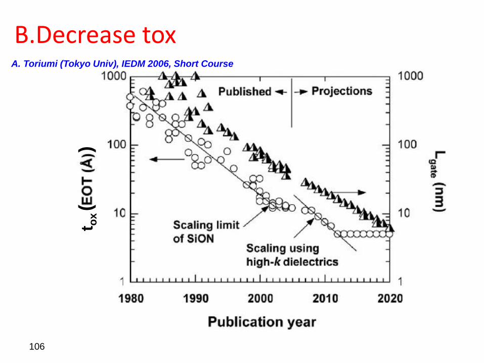
A. Toriumi (Tokyo Univ), IEDM 2006, Short Course
t ox(
(
106
B.Decrease tox

107
C. Configuration change for channel and gate structures for better control of channel potential.
Fin-FET, ET-SOI, etc.
Also, decrease tSi

1V0V
0V
S
0V
0V <V<1V
1V0V
0V
0V
0VS D
G
G
G
Extremely Thin (or Fully-Depleted) SOI
Planar ET (or FD) SOI 108
Si
SiO2
Extremely
thin Si
Drain bias
induced
depletion
- Make Si layer thin (decrease tSi)
- Control channel potential also from the bottom

1V0V
0V
S
0V
0V <V<1V
1V0V
0V
0V
0VS D
G
G
G
Surrounding gate structure (Multiple gates)
PlanarMulti gate 109
Si fin or
nanowire
Drain bias
induced
depletion
- Make Si layer thin(decrease tSi)
- Control channel potential also by multiple gates
not only from top & bottom but maybe also
from side

Fin Tri-gate
(Variation)
-gate All-around
G G G
G
G
Multi-gate structures
110
G
Tri-gate
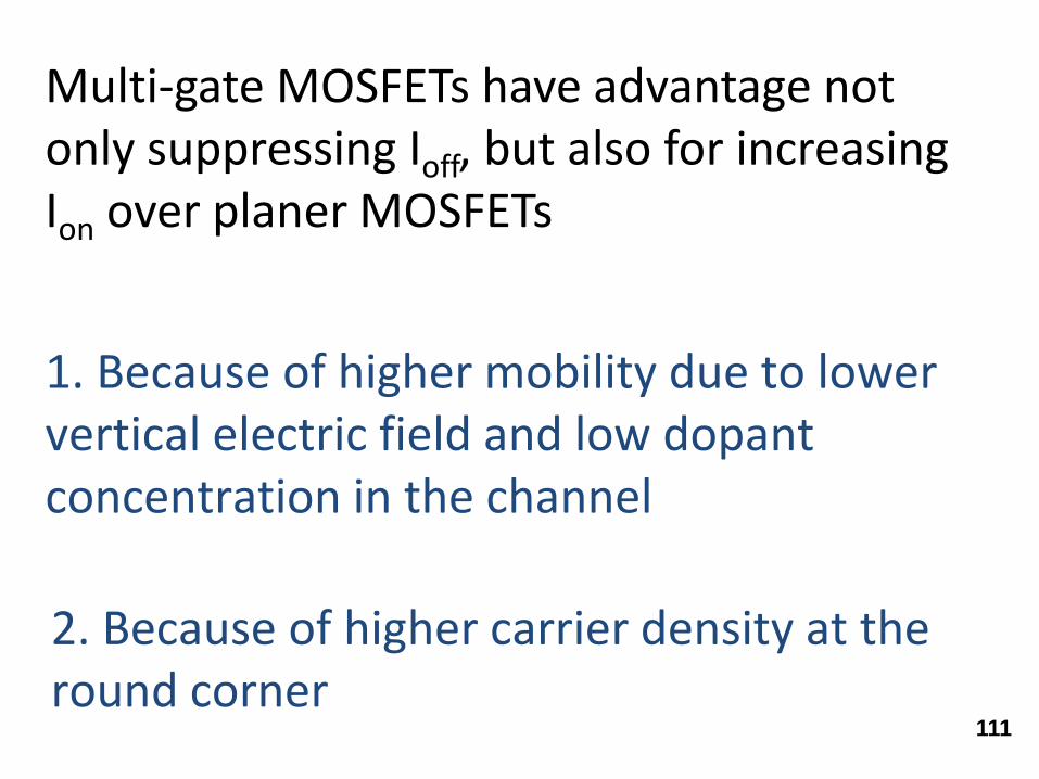
Multi-gate MOSFETs have advantage not only suppressing Ioff, but also for increasing Ion over planer MOSFETs
111
1. Because of higher mobility due to lower vertical electric field and low dopant concentration in the channel
2. Because of higher carrier density at the round corner

112

0.E+00
1.E+19
2.E+19
3.E+19
4.E+19
5.E+19
6.E+19
0 2 4 6 8Distance from SiNW Surface (nm)
6
5
4
3
2
1
0
角の部分
平らな部分
電子濃度(x1019cm-3)Electron Density
Edge portion
Flat portion
113

114
2. Direct-tunneling between S and D
Wave function of electron penetrates the channel potential barriers by quantum mechanical physics, when the channel length is around 3 nm.

Tunnelingdistance
3 nm
Source DrainChannel
115
Ene
rgy o
r P
ote
ntia
l
for
Ele
ctr
on
Direct-tunnelcurrent
There is no solutions!
Downsizing limit is @ Lg 3 nm.
Built-in potential
between Source
and Channel pn
junction < 0.7 V
When transistor is at off state

116
Vg
Id
Vth
(Threshold Voltage)
Vg=0V
Subthreshould
Leakage Current
3.Subtheshold leakage current of MOSFET
ONOFF
Ion
Subthreshold
region

117
Vg (V)1
0.3 V
0.5 V 1.0 V
Ion
Ioff
Id (A/mm)
10-7
10-5
10-11
10-9
Vd
Vth
0.15 V
0 0.5
Subthreshold leakage current
Electron Energy
Boltzmann statics
Exp (qV/kT)
Lg 1/2
Vd, Vg 1/2
Vth 1/2
Ioff 103 in this example
However
Because of
log-linear dependence

118
Vg
Id
Vth
(Threshold Voltage)
Vg=0V
Subthreshould
Leakage Current
Subtheshold leakage current of MOSFET
Subthreshold Current
Is OK at Single Tr. level
But not OK
For Billions of Trs.
ONOFF
Ion
Subthreshold
region

119
3. Subthreshold current between S and D
Solution: however very difficult
Keep Vth as high as possible
- Do not decrease supply voltage, Vd
- Suppress variability in Vth
However, punchthough enhanced
Thus, subthreshold current will limit the downsizing, especially for mobile devices

120
4. Gate leakage current
Probably OK using high-k, until EOT=0.4 nm
1.E-02
1.E-01
1.E+00
1.E+01
1.E+02
1.E+03
1.E+04
0.3 0.4 0.5 0.6 0.7 0.8
ITRS requirement
Jg
at 1
V (
A/c
m2)
EOT (nm)
Gate Leakage current
H. Iwai, SBMicro 2013
La silicate
Gate dielectrics

0 0.2 0.4 0.6 0.8 1.0
Drain Voltage (V)
0.2
0.4
0.6
0.8
1.0
Dra
in C
urr
en
t (m
A)
Vg= 0.4V
Vg= 0.6V
Vg= 0.8V
Vg= 1.0V
Vg= 0.2V
Vg= 0 V
L/W = 5/20mm
T = 300K
Nsub = 3×1016cm-3
0
20
40
60
80
100
120
140
0 0.5 1 1.5 2 2.5
EOT = 0.40nm
L/W = 5/20mm
T = 300K
Nsub = 3×1016cm-3
Eeff [MV/cm]
Ele
ctr
on
Mo
bilit
y [
cm
2/V
sec]
EOT=0.40nm
Our Work at TIT: High-k
121
Our result at TIT

All the 4 leakage components increase, when downsizing
1. Punch through current between S and D
2. Subthreshold current between S and D
3. Direct-tunneling current between S and D
4. Gate leakage current between G and S/B/D
Solution: Enhance gate bias control to channel potential
Decrease tox (EOT) for gate oxide, and tSi for SOI & Fin FETs
Solution: Keep as high Vth as possible
Keep as high Vsupply as possible, but difficult
This will limit the downsizing depending on application
before Lg = ~ 3 nm
No solution. Limit the downsizing at Lg = ~ 3 nm
Solution. Introduction of new material for higher k and band offset122

123
Subthreshold Leakage (A/mm)
Op
era
tio
n F
req
ue
nc
y (
a.u
.)
e)
100
10
1
Source: 2007 ITRS Winter Public Conf.
The limit is deferent depending on application

How far can we go for production?
10mm 8mm 6mm 4mm 3mm 2mm 1.2mm 0.8mm 0.5mm
0.35mm 0.25mm 180nm 130nm 90nm 65nm 45nm 32nm
(28nm) 22nm 14nm 10 nm 7nm 5nm? 3.5nm? 2.5 nm?
Past
Now Future
124
Intermediate
node
Direct-tunnelSubthreshold
punchthrough
Limit depending on applications
Fundamentallimit

However, careful about the commercial name of technology!
22 nm Technology by Intel
Lg (Gate length) = 30 nm (HP), 34 nm (MP), 34 nm or larger (SP)
IEDM 2012, VLSI 2013
10 nm Technology by Leti (FD-SOI)
Lg (Gate length) = 25 nm Euro SOI 2014
Recently,
Gate length (Lg) is much larger than the Technology name
14 nm Technology by Global
Lg (Gate length) = 15 nm ECS Fall 2013
125

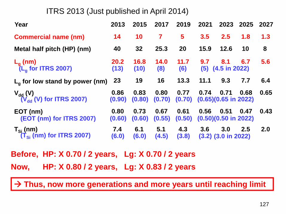
ITRS 2013 (Just published in April 2014)
Lg (nm)
Metal half pitch (nm)
Commercial name (nm)
Vdd (V)
EOT (nm)
TSi (nm)
X 0.70 / 2 years
X 0.80 / 2 years
X 0.83 / 2 years
X 0.96 / 2 years
X 0.91 / 2 years
X 0.84 / 2 years
Only the commercial names decreases X0.7/ 2 years
Year 2027
1.3 (nm)
8 (nm)
5.6 (nm)
0.43 (nm)
0.65 (nm)
2.0 (nm)
Year 2013
14 (nm)
40 (nm)
20.2 (nm)
0.80 (nm)
0.86 (nm)
7.4 (nm)
Difference between the commercial name and
physical parameters becomes larger
1.3 nm technology!
but HP = 8nm
Lg = 5.6 nm
Recently, companies become not to disclose Lg values at conferences
126
2015 2017 2019 20252021 2023 20272013
10 7 5 1.83.5 2.5 1.314
32 25.3 20 1015.9 12.6 840
19 16 13.3 7.711.1 9.3 6.423
16.8 14.0 11.7 6.79.7 8.1 5.620.2(10) (8) (6) (5)(13)
0.73 0.67 0.61 0.470.56 0.51 0.430.80(0.60) (0.55) (0.50) (0.50)(0.60)
0.83 0.80 0.77 0.680.74 0.71 0.650.86(0.80) (0.70) (0.70) (0.65)(0.90)
6.1 5.1 4.3 2.53.6 3.0 2.07.4(6.0) (4.5) (3.8) (3.2)(6.0)
Year
Lg (nm)
Metal half pitch (HP) (nm)
(Lg for ITRS 2007)
Commercial name (nm)
Lg for low stand by power (nm)
Vdd (V) (Vdd (V) for ITRS 2007)
EOT (nm) (EOT (nm) for ITRS 2007)
TSi (nm) (TSi (nm) for ITRS 2007)
(4.5 in 2022)
(3.0 in 2022)
(0.50 in 2022)
(0.65 in 2022)
ITRS 2013 (Just published in April 2014)
Now, HP: X 0.80 / 2 years, Lg: X 0.83 / 2 years
Thus, now more generations and more years until reaching limit
Before, HP: X 0.70 / 2 years, Lg: X 0.70 / 2 years
127

http://download.intel.com/newsroom/kits/1
4nm/pdfs/Intel_14nm_New_uArch.pdf
SRAM area
Logic area
Shrink rate
Intel kept X ~0.7 for pitch
until 14 nm technology,
but it is not certain for future
128

Degradation of on-current
when downsizing
129

When downsizing
1.Mobility degradation
2.Carrier density decrease
1, 2 decrease of on-current
130

m(mobility) degradation
tSi Si
tSi
Si
tSi
Si
tSi
Nano-wire Fin / Tri
SOI
tox
m
Gate electrode
Si channel
Gate oxidetox
Gate stack
Metal/
Oxide
interface
d
d
d
d
d
d
d
d dd
d
d
d
Si surface
d
Strong interaction between
carriers and metal/oxide interface
Strong interaction between
carriers and Si surface (or interface)
m
d
131

0
50
100
150
200
250
300
0.3 0.4 0.5 0.6 0.7 0.8 0.9 1
EOT (nm)
Mo
bili
ty (
cm
2/V
se
c)
at 1 MV/cm
Open : Hf-based oxidesSolid : La-silicate oxide
K. Uchida et al., pp.47, IEDM2002 (Toshiba)T. Kawanago, et al., (Tokyo Tech.) T-ED, 2012
T. Ando, et al., (IBM) IEDM 2009
L.-Å. Ragnarsson, et al., (IMEC) Microelectron. Eng,. 2011.
2015 2017 2019 20252021 2023 20272013Year
10 7 5 1.83.5 2.5 1.314Commercial name (nm)
6.1 5.1 4.3 2.53.6 3.0 2.07.4TSi (nm)
0.73 0.67 0.61 0.470.56 0.51 0.430.80EOT (nm)
ITRS 2013
toxtSim m
132

Carrier density decrease
2015 2017 2019 20252021 2023 20272013Year
10 7 5 1.83.5 2.5 1.314Commercial name (nm)
6.1 5.1 4.3 2.53.6 3.0 2.07.4TSi (nm)
ITRS 2013
tSi Volume DOS Carrier density
Si nanowire
band structure
1 nm 2 nm 3 nm 4 nm 6 nm
Iwata et al., Journal of Computational Physics 229 (2010) 2339–2363
Diameter
133
4. Summary and
conclusions
134

Summary and conclusions
Si-MOSFET is the main component nano-CMOS devices
and will be so in future.
While the shrink rate of commercial node name will keep
0.7 for 2 years, the shrink rates of HP, Lg, Vd, tox, tSi are
expected to be are expected to be, 0.80, 0.83. 0.96, 91
and 0.84, respectively, according to ITRS. Because of
many reasons, the rate of physical shrinking will be smaller
as the downsizing reach near the limit.
Increase of the Ioff due to subthreshhold leakage and
degradation of Ion due to EOT and tSi reduction would limit
the gate length scaling before Lg reaches its limit of direct-
tunneling (@ Lg = ~3nm).
135

Summary and conclusions (continued)
Problems and cost of the lithography and interconnects
would also the limit the downsizing.
There have been good challenges for the emerging
technologies such as alternative channel, T-FET, 2D
material and others. However, none of those technologies
has yet reached the level for the industry to start R&D
assuming mass production, such as yield, variability,
reliability, large wafer production.
136

Acknowledgement
Slides for the 2D materials were made by Prof.
Hitoshi Wakabayashi, Tokyo Institute of Technology.
Many slides except for the 2D materials were made
by Dr. Takamasa Kawanago, Dr. Darius Zade, and
Mr. Tomoya Shoji of Tokyo Institute of Technology,
and Mr. Jing Neng Yao of National Chio Tung
University.
I would like to express appreciation to the following
people for the great support for preparing the
materials for the tutorial.
137

Thank you for your attention!
138