Embed Size (px)
Citation preview

REV. 1.9 FS325-DS-19_EN JUN 2015
Datasheet
FS325 One Cell Lithium-ion/Polymer Battery Protection IC
FORTU
NE'
Propert
ies
For R
eferen
ce O
nly

Fortune Semiconductor Corporation
富晶電子股份有限公司
23F., No.29-5,Sec. 2, Zhongzheng E. Rd., Danshui Dist, New Taipei City 251, Taiwan Tel.:886-2-28094742 Fax:886-2-28094874 www.ic-fortune.com
This manual contains new product information. Fortune Semiconductor Corporation reserves the rights to modify the product specification without further notice. No liability is assumed by Fortune Semiconductor
Corporation as a result of the use of this product. No rights under any patent accompany the sale of the product.
FORTU
NE'
Propert
ies
For R
eferen
ce O
nly

1. General Description
FS325 is a series of lithium-ion and lithium-polymer rechargeable battery protection ICs with high accurate voltage detection and delay circuits.
These ICs are suitable for protection of single cell lithium-ion or lithium polymer battery packs from over charge, over discharge and over current.
2. Features
Low supply current
Normal Operation : 2.5μA typ. @VDD=3.9V
Power-down mode : 0.05μA typ. @VDD=2.0V
Auto recovery function : 1.8 μ A typ.
@VDD=2.0V
Overcharge detection voltage﹝VOCU﹞
4.25V~4.31V, Accuracy of 25mV
Overcharge release voltage﹝VOCR﹞
4.05V~4.11V, Accuracy of 50mV
Overdischarge detection voltage﹝VODL﹞
2.30V~2.40V, Accuracy of 100mV
Overdischarge release voltage﹝VODR﹞
2.30V~2.90V, Accuracy of 100mV
Over current detection voltage﹝VOI1﹞
0.10V~0.13V, Accuracy of 10mV
Short circuit detection voltage﹝VOI2﹞
0.7V~0.9V, Accuracy of 10mV
Charger over current detection voltage
﹝VCH﹞-0.09V~0.10V, Accuracy of 20mV
Delay times are generated by an internal circuit. (External capacitors are unnecessary.)
Reset resistance for Over current protection >150k
Wide supply voltage range 1.5 ~ 5.5V
Small package SOT-23-5、SSON-6
0V-Battery charging function
.
3. Ordering Information
FS325 x - x
N6A、N6C Package code
Serial code from A to D * (N6A:1.8*2.0mm SSON-6 Green-Package)
(N6C:1.6*1.6mm SSON-6 Green-Package)
*: Refer to the product name list on next page.
4. Applications
Protection IC for One-Cell Lithium-Ion /
Lithium-Polymer Battery Pack
FORTU
NE'
Propert
ies
For R
eferen
ce O
nly

5. Product Name List
Model Package
Overcharge
detection
voltage
[VOCU] (V)
Overcharge
release
voltage
[VOCR] (V)
Overdischarge
detection
voltage
[VODL] (V)
Overdischarge
release
voltage
[VODR] (V)
Overcurrent
detection
voltage
[VOI1] (V)
Charger over
current
detection
voltage
[VCH] (V)
0V change
function
Standby
function
release
FS325A SOT-23-5 4.310±25mV 4.110±50mV 2.300±77mV 2.300±77mV 0.130±10mV -0.090±20mV YES Connection
of charger
FS325B SOT-23-5 4.250±25mV 4.050±50mV 2.400±100mV 2.900±100mV 0.100±10mV - YES AUTO
recovery
FS325C SOT-23-5 4.275±25mV Note: 1 2.300±100mV 2.300±100mV 0.100±10mV -0.100±20mV YES Connection of charger
FS325D SOT-23-5 4.280±25mV 4.080±50mV 2.300±100mV 2.300±100mV 0.130±10mV -0.100±20mV 0.65V Connection of charger
FS325D-N6A SSON-6 (1.8×2.0) 4.280±25mV 4.080±50mV 2.300±100mV 2.300±100mV 0.130±10mV -0.100±20mV 0.65V
Connection of charger
FS325D-N6C SSON-6 (1.6×1.6) 4.280±25mV 4.080±50mV 2.300±100mV 2.300±100mV 0.130±10mV -0.100±20mV 0.65V
Connection of charger
Note: 1. FS325C VOCR release conditions : VDD<VOCU & VCSI>VOI1 (100mV) 2. FS325D series 0V charging prohibit range: 0.4V~1.1V (typ=0.65V) 3. FS325D-N6C SSON-6 similar to Seiko SNT-6A Package
FORTU
NE'
Propert
ies
For R
eferen
ce O
nly

6. Pin Configuration and Package Marking Information
Pin No. Symbol Description
1 CSI Input pin for current sense, charger detect
2 VDD Positive power input pin
3 VSS Negative power input pin
4 OD FET gate connection pin for discharge control
5 OC FET gate connection pin for charge control
Top Top Point:Lot No.
Bottom Point:Year w : week, A~Z & A ~ Z
Pin No. Symbol Description
1 NC NC
2 OC FET gate connection pin for charge control
3 OD FET gate connection pin for discharge control
4 VSS Negative power input pin
5 VDD Positive power input pin
6 CSI Input pin for current sense, charger detect
3 5 D (1)(2)(3)(4)(5)
(1):Year Code, 0 ~ 9 (2) (3):Week Code, 01 ~ 54 (4) (5):Serial Code, 01 ~ 99
SSON-6(N6A)
Top View
123
4 5 6
Bottom View
5
FORTU
NE'
Propert
ies
For R
eferen
ce O
nly

Pin No. Symbol Description
1 NC NC
2 OC FET gate connection pin for charge control
3 OD FET gate connection pin for discharge control
4 VSS Negative power input pin
5 VDD Positive power input pin
6 CSI Input pin for current sense, charger detect
(2)(3)(4)(5)3 5 D (1)
(1):Year Code, 0 ~ 9 (2) (3):Week Code, 01 ~ 54 (4) (5):Serial Code, 01 ~ 99 __:Pin1 mark
Bottom View
Top View
SSON-6
(N6C)
1 2
456
3
FORTU
NE'
Propert
ies
For R
eferen
ce O
nly

7. Functional Block Diagram
VSS
OC
VSS
VSS
VSS
VDD
VSS
CSI
ChargerDetector
OD
ControlLogic
Short circuitDetector
Over currentDetector
OscillatorControlCircuitOvercharge
Detector
Overdischarge Detector
DividerControlLogic
8. Typical Application Circuit
FORTU
NE'
Propert
ies
For R
eferen
ce O
nly
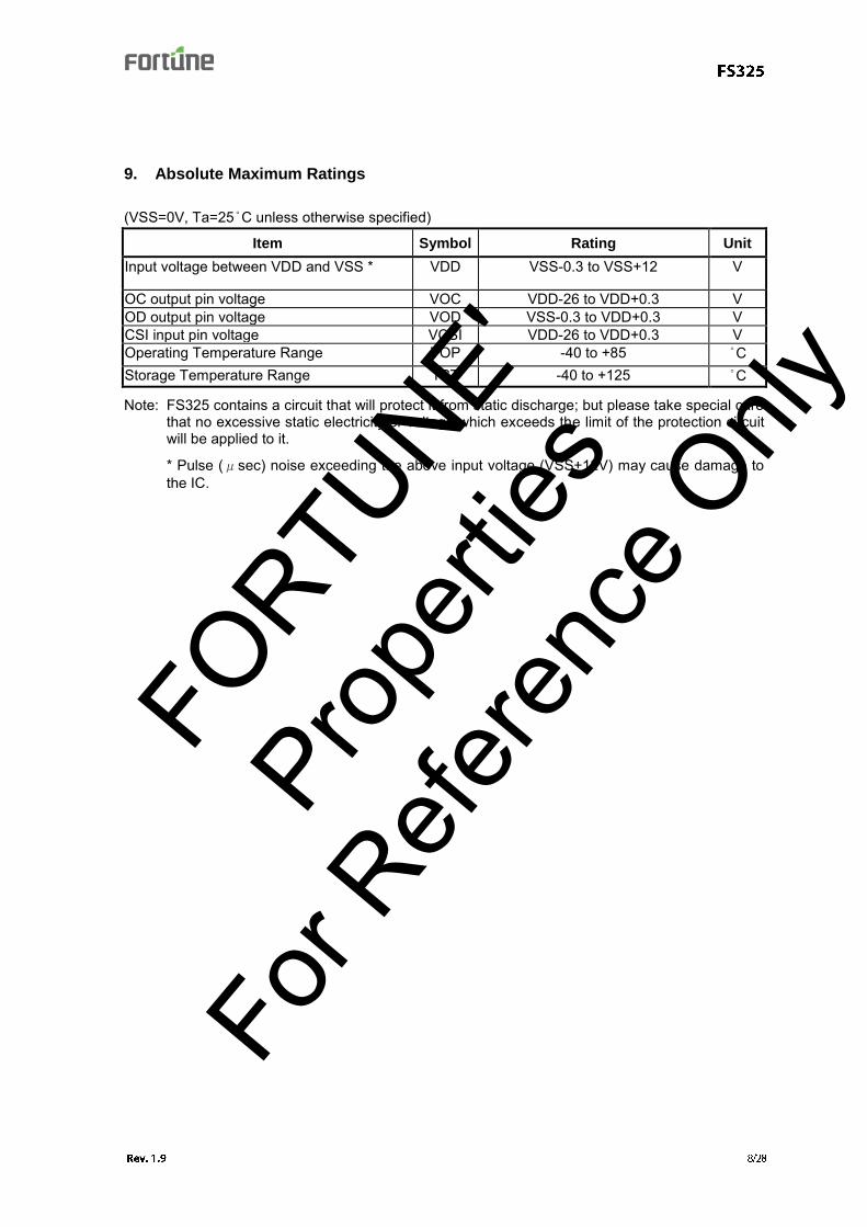
9. Absolute Maximum Ratings
(VSS=0V, Ta=25°C unless otherwise specified)
Item Symbol Rating Unit
Input voltage between VDD and VSS * VDD VSS-0.3 to VSS+12 V
OC output pin voltage VOC VDD-26 to VDD+0.3 V OD output pin voltage VOD VSS-0.3 to VDD+0.3 V CSI input pin voltage VCSI VDD-26 to VDD+0.3 V Operating Temperature Range TOP -40 to +85 °C Storage Temperature Range TST -40 to +125 °C
Note: FS325 contains a circuit that will protect it from static discharge; but please take special care that no excessive static electricity or voltage which exceeds the limit of the protection circuit will be applied to it.
* Pulse (μsec) noise exceeding the above input voltage (VSS+12V) may cause damage to the IC.
FORTU
NE'
Propert
ies
For R
eferen
ce O
nly

10. Electrical Characteristics
FS325A(VSS=0V, Ta=25°C unless otherwise specified) PARAMETER CONDITIONS SYMBOL Min Typ Max UNIT
CURRENT CONSUMPTION Supply Current VDD=3.9V IDD 2.5 5.2 μA Power-Down Current VDD=2.0V IPD 0.05 1.0 μA OPERATING VOLTAGE Operating input voltage1 VDD-VSS VDS1 1.5 5.5 V Operating input voltage2 VDD-CSI VDS2 1.5 V DETECTION VOLTAGE Overcharge detection voltage VOCU 4.285 4.310 4.335 V Overcharge release voltage VOCR 4.060 4.110 4.160 V Overdischarge detection voltage VODL 2.223 2.300 2.377 V Overdischarge release voltage VODR 2.223 2.300 2.377 V Over current detection voltage VOI1 0.120 0.130 0.140 V Short circuit detection voltage VDD=3.6V VOI2 0.80 0.90 1.00 V Charger over current detection voltage VDD=3.6V VCH -0.11 -0.09 -0.07 V Release pull up resistor VDD=2.0V,CS=VDD-1.0V Rdown 75 150 300 kohm Release pull down resistor VDD=3.6V,CS=VDD Rshort 15 30 150 kohm Faulty charger detect voltage Vdet 5.5 8.0 10.5 V Faulty charger recovery voltage Vrec 5.3 7.3 9.3 V 0V charging prohibit VST 0 0 0 V Power-Down detect voltage Vstd 0.3VCC 0.5VCC 0.7VCC V DELAY TIME Overcharge detection delay time VDD=4.0V to 4.4V TOC 4 6.25 8.5 s Overdischarge detection delay time VDD=3.0V to 2.0V TOD 65 100 135 ms Over current detection delay time VDD=3.6V TOI1 7.365 11.0 14.25 ms Short circuit detection delay time VDD=3.6V TOI2 0.45 0.750 1.4 ms Charger over current delay time VDD=3.6V Tdet 16.25 32.5 48.75 ms Overcharge timer reset delay time Td1 5.0 16 50.0 ms Charge release delay time Td2 5.0 16 50.0 ms Charge connection detection delay Tdr1 0.3 1 3.0 ms OTHER
Output high level voltage VDD=3.6V, Ioh=-20μA , CSI=0V OC,OD VOH 3.1 V
Output low level voltage VDD=3.6V, Ioh=+20μA , CSI=0V OC,OD VOL 0.5 V
FORTU
NE'
Propert
ies
For R
eferen
ce O
nly

FS325A(VSS=0V, Ta=-5 to +55°C unless otherwise specified)
PARAMETER CONDITIONS SYMBOL Min Typ Max UNIT
CURRENT CONSUMPTION Supply Current VDD=3.9V IDD 2.5 5.5 μA Power-Down Current VDD=2.0V IPD 0.05 1.0 μA OPERATING VOLTAGE Operating input voltage1 VDD-VSS VDS1 1.5 5.5 V Operating input voltage2 VDD-CSI VDS2 1.5 V DETECTION VOLTAGE Overcharge detection voltage VOCU 4.280 4.310 4.340 V Overcharge release voltage VOCR 4.060 4.110 4.160 V Overdischarge detection voltage VODL 2.223 2.300 2.377 V Overdischarge release voltage VODR 2.223 2.300 2.377 V Over current detection voltage VOI1 0.120 0.130 0.140 V Short circuit detection voltage VDD=3.6V VOI2 0.80 0.90 1.00 V Charger over current detection voltage VDD=3.6V VCH -0.11 -0.09 -0.07 V Release pull up resistor VDD=2.0V,CS=VDD-1.0V Rdown 75 150 300 kohm Release pull down resistor VDD=3.6V,CS=VDD Rshort 15 30 150 kohm Faulty charger detect voltage Vdet 6.0 8.0 10.0 V Faulty charger recovery voltage Vrec 5.8 7.3 8.8 V 0V charging prohibit VST 0 0 0 V Power-Down detect voltage Vstd 0.3VCC 0.5VCC 0.7VCC V DELAY TIME Overcharge detection delay time VDD=4.0V to 4.4V TOC 3.125 6.25 9.375 s Overdischarge detection delay time VDD=3.0V to 2.0V TOD 50 100 150 ms Over current detection delay time VDD=3.6V TOI1 5.5 11.0 16.85 ms Short circuit detection delay time VDD=3.6V TOI2 0.37 0.75 1.48 ms Charger over current delay time VDD=3.6V Tdet 13 32.5 76.5 ms Overcharge timer reset delay time Td1 5.0 16 50.0 ms Charge release delay time Td2 5.0 16 50.0 ms Charge connection detection delay Tdr1 0.3 1 3.0 ms OTHER
Output high level voltage VDD=3.6V, Ioh=-20μA , CSI=0V OC,OD VOH 3.1 V
Output low level voltage VDD=3.6V, Ioh=+20μA , CSI=0V OC,OD VOL 0.5 V
FORTU
NE'
Propert
ies
For R
eferen
ce O
nly

FS325A(VSS=0V, Ta=-30 to +70°C unless otherwise specified)
PARAMETER CONDITIONS SYMBOL Min Typ Max UNIT
CURRENT CONSUMPTION Supply Current VDD=3.9V IDD 2.5 6 μA Power-Down Current VDD=2.0V IPD 0.05 1.0 μA OPERATING VOLTAGE Operating input voltage1 VDD-VSS VDS1 1.5 5.5 V Operating input voltage2 VDD-CSI VDS2 1.7 V DETECTION VOLTAGE Overcharge detection voltage VOCU 4.245 4.310 4.345 V Overcharge release voltage VOCR 4.025 4.110 4.165 V Overdischarge detection voltage VODL 2.223 2.300 2.377 V Overdischarge release voltage VODR 2.223 2.300 2.377 V Over current detection voltage VOI1 0.115 0.130 0.145 V Short circuit detection voltage VDD=3.6V VOI2 0.80 0.90 1.00 V Charger over current detection voltage VDD=3.6V VCH -0.115 -0.09 -0.065 V Release pull up resistor VDD=2.0V,CS=VDD-1.0V Rdown 75 150 300 kohm Release pull down resistor VDD=3.6V,CS=VDD Rshort 15 30 150 kohm Faulty charger detect voltage Vdet 5.5 8.0 10.5 V Faulty charger recovery voltage Vrec 5.3 7.3 9.3 V 0V charging prohibit VST 0 0 0 V Power-Down detect voltage Vstd 0.3VCC 0.5VCC 0.7VCC V DELAY TIME Overcharge detection delay time VDD=4.0V to 4.4V TOC 2.50 6.25 10.60 s Overdischarge detection delay time VDD=3.0V to 2.0V TOD 40 100 170 ms Over current detection delay time VDD=3.6V TOI1 5.0 11.0 20.0 ms Short circuit detection delay time VDD=3.6V TOI2 0.225 0.75 2.000 ms Charger over current delay time VDD=3.6V Tdet 13.0 32.5 76.5 ms Overcharge timer reset delay time Td1 5.0 16 50.0 ms Charge release delay time Td2 5.0 16 50.0 ms Charge connection detection delay Tdr1 0.3 1 3.0 ms OTHER
Output high level voltage VDD=3.6V, Ioh=-20μA , CSI=0V OC,OD VOH 3.1 V
Output low level voltage VDD=3.6V, Ioh=+20μA , CSI=0V OC,OD VOL 0.5 V
FORTU
NE'
Propert
ies
For R
eferen
ce O
nly
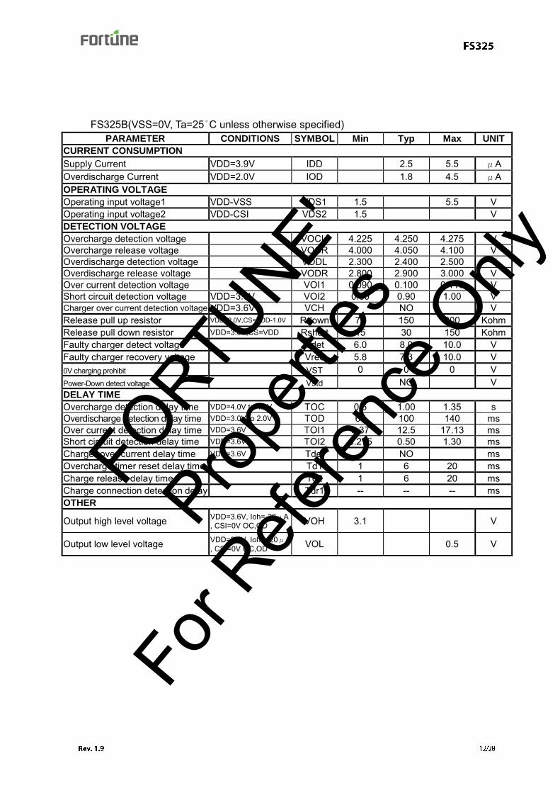
FS325B(VSS=0V, Ta=25°C unless otherwise specified)
PARAMETER CONDITIONS SYMBOL Min Typ Max UNIT
CURRENT CONSUMPTION Supply Current VDD=3.9V IDD 2.5 5.5 μA Overdischarge Current VDD=2.0V IOD 1.8 4.5 μA OPERATING VOLTAGE Operating input voltage1 VDD-VSS VDS1 1.5 5.5 V Operating input voltage2 VDD-CSI VDS2 1.5 V DETECTION VOLTAGE Overcharge detection voltage VOCU 4.225 4.250 4.275 V Overcharge release voltage VOCR 4.000 4.050 4.100 V Overdischarge detection voltage VODL 2.300 2.400 2.500 V Overdischarge release voltage VODR 2.800 2.900 3.000 V Over current detection voltage VOI1 0.090 0.100 0.110 V Short circuit detection voltage VDD=3.6V VOI2 0.80 0.90 1.00 V Charger over current detection voltage VDD=3.6V VCH NO V Release pull up resistor VDD=2.0V,CS=VDD-1.0V Rdown 75 150 300 Kohm Release pull down resistor VDD=3.6V,CS=VDD Rshort 15 30 150 Kohm Faulty charger detect voltage Vdet 6.0 8.0 10.0 V Faulty charger recovery voltage Vrec 5.8 7.3 10.0 V 0V charging prohibit VST 0 0 0 V Power-Down detect voltage Vstd NO V DELAY TIME Overcharge detection delay time VDD=4.0V to 4.4V TOC 0.6 1.00 1.35 s Overdischarge detection delay time VDD=3.0V to 2.0V TOD 65 100 140 ms Over current detection delay time VDD=3.6V TOI1 8.37 12.5 17.13 ms Short circuit detection delay time VDD=3.6V TOI2 0.275 0.50 1.30 ms Charger over current delay time VDD=3.6V Tdet NO ms Overcharge timer reset delay time Td1 1 6 20 ms Charge release delay time Td2 1 6 20 ms Charge connection detection delay Tdr1 -- -- -- ms OTHER
Output high level voltage VDD=3.6V, Ioh=-20μA , CSI=0V OC,OD VOH 3.1 V
Output low level voltage VDD=3.6V, Ioh=+20μA , CSI=0V OC,OD VOL 0.5 V
FORTU
NE'
Propert
ies
For R
eferen
ce O
nly

FS325B(VSS=0V, Ta=-5 to +55°C unless otherwise specified)
PARAMETER CONDITIONS SYMBOL Min Typ Max UNIT
CURRENT CONSUMPTION Supply Current VDD=3.9V IDD 2.5 5.5 μA Overdischarge Current VDD=2.0V IOD 1.8 4.5 μA OPERATING VOLTAGE Operating input voltage1 VDD-VSS VDS1 1.5 5.5 V Operating input voltage2 VDD-CSI VDS2 1.5 V DETECTION VOLTAGE Overcharge detection voltage VOCU 4.220 4.250 4.280 V Overcharge release voltage VOCR 4.000 4.050 4.100 V Overdischarge detection voltage VODL 2.300 2.400 2.500 V Overdischarge release voltage VODR 2.800 2.900 3.000 V Over current detection voltage VOI1 0.090 0.100 0.110 V Short circuit detection voltage VDD=3.6V VOI2 0.80 0.90 1.00 V Charger over current detection voltage VDD=3.6V VCH NO V Release pull up resistor VDD=2.0V,CS=VDD-1.0V Rdown 75 150 300 Kohm Release pull down resistor VDD=3.6V,CS=VDD Rshort 15 30 150 Kohm Faulty charger detect voltage Vdet 6.0 8.0 10.0 V Faulty charger recovery voltage Vrec 5.8 7.3 10.0 V 0V charging prohibit VST 0 0 0 V Power-Down detect voltage Vstd NO V DELAY TIME Overcharge detection delay time VDD=4.0V to 4.4V TOC 0.5 1.00 1.5 s Overdischarge detection delay time VDD=3.0V to 2.0V TOD 50 100 150 ms Over current detection delay time VDD=3.6V TOI1 6.25 12.5 19.1 ms Short circuit detection delay time VDD=3.6V TOI2 0.25 0.50 1.50 ms Charger over current delay time VDD=3.6V Tdet NO ms Overcharge timer reset delay time Td1 1 6 20 ms Charge release delay time Td2 1 6 20 ms Charge connection detection delay Tdr1 -- -- -- ms OTHER
Output high level voltage VDD=3.6V, Ioh=-20μA , CSI=0V OC,OD VOH 3.1 V
Output low level voltage VDD=3.6V, Ioh=+20μA , CSI=0V OC,OD VOL 0.5 V
FORTU
NE'
Propert
ies
For R
eferen
ce O
nly

FS325B(VSS=0V, Ta=-30 to +70°C unless otherwise specified)
PARAMETER CONDITIONS SYMBOL Min Typ Max UNIT
CURRENT CONSUMPTION Supply Current VDD=3.9V IDD 2.5 6 μA Overdischarge Current VDD=2.0V IOD 1.8 5 μA OPERATING VOLTAGE Operating input voltage1 VDD-VSS VDS1 1.5 5.5 V Operating input voltage2 VDD-CSI VDS2 1.5 V DETECTION VOLTAGE Overcharge detection voltage VOCU 4.185 4.250 4.285 V Overcharge release voltage VOCR 3.965 4.050 4.105 V Overdischarge detection voltage VODL 2.300 2.400 2.500 V Overdischarge release voltage VODR 2.800 2.900 3.000 V Over current detection voltage VOI1 0.085 0.100 0.115 V Short circuit detection voltage VDD=3.6V VOI2 0.80 0.90 1.00 V Charger over current detection voltage VDD=3.6V VCH NO V Release pull up resistor VDD=2.0V,CS=VDD-1.0V Rdown 75 150 300 Kohm Release pull down resistor VDD=3.6V,CS=VDD Rshort 15 30 150 Kohm Faulty charger detect voltage Vdet 5.5 8.0 10.5 V Faulty charger recovery voltage Vrec 5.3 7.3 9.3 V 0V charging prohibit VST 0 0 0 V Power-Down detect voltage Vstd NO V DELAY TIME Overcharge detection delay time VDD=4.0V to 4.4V TOC 0.4 1.00 1.7 s Overdischarge detection delay time VDD=3.0V to 2.0V TOD 40 100 170 ms Over current detection delay time VDD=3.6V TOI1 5.00 12.5 21.6 ms Short circuit detection delay time VDD=3.6V TOI2 0.2 0.50 1.80 ms Charger over current delay time VDD=3.6V Tdet NO ms Overcharge timer reset delay time Td1 1 6 20 ms Charge release delay time Td2 1 6 20 ms Charge connection detection delay Tdr1 -- -- -- ms OTHER
Output high level voltage VDD=3.6V, Ioh=-20μA , CSI=0V OC,OD VOH 3.1 V
Output low level voltage VDD=3.6V, Ioh=+20μA , CSI=0V OC,OD VOL 0.5 V
FORTU
NE'
Propert
ies
For R
eferen
ce O
nly

FS325C(VSS=0V, Ta=25°C unless otherwise specified)
PARAMETER CONDITIONS SYMBOL Min Typ Max UNIT
CURRENT CONSUMPTION Supply Current VDD=3.9V IDD 2.5 5.5 μA Power-Down Current VDD=2.0V IPD 0.05 1.0 μA OPERATING VOLTAGE Operating input voltage1 VDD-VSS VDS1 1.5 5.5 V Operating input voltage2 VDD-CSI VDS2 1.5 V DETECTION VOLTAGE Overcharge detection voltage VOCU 4.250 4.275 4.300 V Overcharge release voltage VOCR VDD<VOCU & VCSI>VOI1 V Overdischarge detection voltage VODL 2.200 2.300 2.400 V Overdischarge release voltage VODR 2.200 2.300 2.400 V Over current detection voltage VOI1 0.090 0.100 0.110 V Short circuit detection voltage VDD=3.6V VOI2 0.80 0.90 1.00 V Charger over current detection voltage VDD=3.6V VCH -0.12 -0.10 -0.08 V Release pull up resistor VDD=2.0V,CS=VDD-1.0V Rdown 75 150 300 Kohm Release pull down resistor VDD=3.6V,CS=VDD Rshort 15 30 150 Kohm Faulty charger detect voltage Vdet 6.0 8.0 10.0 V Faulty charger recovery voltage Vrec 5.8 7.3 8.8 V 0V charging prohibit VST 0 0 0 V Power-Down detect voltage Vstd 0.3VCC 0.5VCC 0.7VCC V DELAY TIME Overcharge detection delay time VDD=4.0V to 4.4V TOC 0.6 1 1.35 s Overdischarge detection delay time VDD=3.0V to 2.0V TOD 65 100 140 ms Over current detection delay time VDD=3.6V TOI1 10.8 16.5 21.6 ms Short circuit detection delay time VDD=3.6V TOI2 0.3 0.50 1.3 ms Charger over current delay time VDD=3.6V Tdet 12.5 25.0 37.5 ms Overcharge timer reset delay time Td1 5.0 16.0 50.0 ms Charge release delay time Td2 5.0 16.0 50.0 ms Charge connection detection delay Tdr1 3.0 8.0 16.0 ms OTHER
Output high level voltage VDD=3.6V, Ioh=-20μA , CSI=0V OC,OD VOH 3.1 V
Output low level voltage VDD=3.6V, Ioh=+20μA , CSI=0V OC,OD VOL 0.5 V
FORTU
NE'
Propert
ies
For R
eferen
ce O
nly

FS325C(VSS=0V, Ta=-5 to +55°C unless otherwise specified)
PARAMETER CONDITIONS SYMBOL Min Typ Max UNIT
CURRENT CONSUMPTION Supply Current VDD=3.9V IDD 2.5 5.5 μA Power-Down Current VDD=2.0V IPD 0.05 1.0 μA OPERATING VOLTAGE Operating input voltage1 VDD-VSS VDS1 1.5 5.5 V Operating input voltage2 VDD-CSI VDS2 1.5 V DETECTION VOLTAGE Overcharge detection voltage VOCU 4.245 4.275 4.305 V Overcharge release voltage VOCR VDD<VOCU & VCSI>VOI1 V Overdischarge detection voltage VODL 2.200 2.300 2.400 V Overdischarge release voltage VODR 2.200 2.300 2.400 V Over current detection voltage VOI1 0.090 0.100 0.110 V Short circuit detection voltage VDD=3.6V VOI2 0.80 0.90 1.00 V Charger over current detection voltage VDD=3.6V VCH -0.12 -0.10 -0.08 V Release pull up resistor VDD=2.0V,CS=VDD-1.0V Rdown 75 150 300 Kohm Release pull down resistor VDD=3.6V,CS=VDD Rshort 15 30 150 Kohm Faulty charger detect voltage Vdet 6.0 8.0 10.0 V Faulty charger recovery voltage Vrec 5.8 7.3 8.8 V 0V charging prohibit VST 0 0 0 V Power-Down detect voltage Vstd 0.3VCC 0.5VCC 0.7VCC V DELAY TIME Overcharge detection delay time VDD=4.0V to 4.4V TOC 0.5 1 1.5 s Overdischarge detection delay time VDD=3.0V to 2.0V TOD 50 100 150 ms Over current detection delay time VDD=3.6V TOI1 8.0 16.5 25.0 ms Short circuit detection delay time VDD=3.6V TOI2 0.25 0.50 1.5 ms Charger over current delay time VDD=3.6V Tdet 5.0 25.0 37.5 ms Overcharge timer reset delay time Td1 5.0 16.0 50.0 ms Charge release delay time Td2 5.0 16.0 50.0 ms Charge connection detection delay Tdr1 3.0 8.0 16.0 ms OTHER
Output high level voltage VDD=3.6V, Ioh=-20μA , CSI=0V OC,OD VOH 3.1 V
Output low level voltage VDD=3.6V, Ioh=+20μA , CSI=0V OC,OD VOL 0.5 V
FORTU
NE'
Propert
ies
For R
eferen
ce O
nly

FS325C(VSS=0V, Ta=-30 to 70°C unless otherwise specified)
PARAMETER CONDITIONS SYMBOL Min Typ Max UNIT
CURRENT CONSUMPTION Supply Current VDD=3.9V IDD 2.5 6 μA Power-Down Current VDD=2.0V IPD 0.05 1.0 μA OPERATING VOLTAGE Operating input voltage1 VDD-VSS VDS1 1.5 5.5 V Operating input voltage2 VDD-CSI VDS2 1.5 V DETECTION VOLTAGE Overcharge detection voltage VOCU 4.240 4.275 4.320 V Overcharge release voltage VOCR VDD<VOCU & VCSI>VOI1 V Overdischarge detection voltage VODL 2.200 2.300 2.400 V Overdischarge release voltage VODR 2.200 2.300 2.400 V Over current detection voltage VOI1 0.085 0.100 0.125 V Short circuit detection voltage VDD=3.6V VOI2 0.80 0.90 1.00 V Charger over current detection voltage VDD=3.6V VCH -0.125 -0.10 -0.075 V Release pull up resistor VDD=2.0V,CS=VDD-1.0V Rdown 75 150 300 Kohm Release pull down resistor VDD=3.6V,CS=VDD Rshort 15 30 150 Kohm Faulty charger detect voltage Vdet 5.5 8.0 10.5 V Faulty charger recovery voltage Vrec 5.3 7.3 9.3 V 0V charging prohibit VST 0 0 0 V Power-Down detect voltage Vstd 0.3VCC 0.5VCC 0.7VCC V DELAY TIME Overcharge detection delay time VDD=4.0V to 4.4V TOC 0.4 1 1.7 s Overdischarge detection delay time VDD=3.0V to 2.0V TOD 40 100 170 ms Over current detection delay time VDD=3.6V TOI1 2.5 14.5 28.9 ms Short circuit detection delay time VDD=3.6V TOI2 0.25 0.50 1.75 ms Charger over current delay time VDD=3.6V Tdet 5.5 25.0 69.0 ms Overcharge timer reset delay time Td1 5.0 16.0 50.0 ms Charge release delay time Td2 5.0 16.0 50.0 ms Charge connection detection delay Tdr1 3.0 8.0 16.0 ms OTHER
Output high level voltage VDD=3.6V, Ioh=-20μA , CSI=0V OC,OD VOH 3.1 V
Output low level voltage VDD=3.6V, Ioh=+20μA , CSI=0V OC,OD VOL 0.5 V
FORTU
NE'
Propert
ies
For R
eferen
ce O
nly

FS325D、FS325D-N6A、FS325D-N6C (VSS=0V, Ta=25°C unless otherwise specified)
PARAMETER CONDITIONS SYMBOL Min Typ Max UNIT
CURRENT CONSUMPTION Supply Current VDD=3.9V IDD 2.5 5.5 μA Power-Down Current VDD=2.0V IPD 0.05 1.0 μA OPERATING VOLTAGE Operating input voltage1 VDD-VSS VDS1 1.5 5.5 V Operating input voltage2 VDD-CSI VDS2 1.5 V DETECTION VOLTAGE Overcharge detection voltage VOCU 4.255 4.280 4.305 V Overcharge release voltage VOCR 4.030 4.080 4.130 V Overdischarge detection voltage VODL 2.200 2.300 2.400 V Overdischarge release voltage VODR 2.200 2.300 2.400 V Over current detection voltage VOI1 0.120 0.130 0.140 V Short circuit detection voltage VDD=3.6V VOI2 0.60 0.70 0.80 V Charger over current detection voltage VDD=3.6V VCH -0.120 -0.100 -0.080 V Release pull up resistor VDD=2.0V,CS=VDD-1.0V Rdown 75 150 300 Kohm Release pull down resistor VDD=3.6V,CS=VDD Rshort 15 30 150 Kohm Faulty charger detect voltage Vdet 6.0 8.0 10.0 V Faulty charger recovery voltage Vrec 5.8 7.3 8.8 V 0V charging prohibit VST 0.40 0.65 1.10 V Power-Down detect voltage Vstd 0.3VCC 0.5VCC 0.7VCC V DELAY TIME Overcharge detection delay time VDD=4.0V to 4.4V TOC 0.6 1 1.35 s Overdischarge detection delay time VDD=3.0V to 2.0V TOD 65 100 140 ms Over current detection delay time VDD=3.6V TOI1 13.3 20.0 26.5 ms Short circuit detection delay time VDD=3.6V TOI2 0.60 1.0 1.80 ms Charger over current delay time VDD=3.6V Tdet - - - ms Overcharge timer reset delay time Td1 5.0 16.0 50.0 ms Charge release delay time Td2 5.0 16.0 50.0 ms Charge connection detection delay Tdr1 0.5 1.0 2.0 ms OTHER
Output high level voltage VDD=3.6V, Ioh=-20μA , CSI=0V OC,OD VOH 3.1 V
Output low level voltage VDD=3.6V, Ioh=+20μA , CSI=0V OC,OD VOL 0.5 V
FORTU
NE'
Propert
ies
For R
eferen
ce O
nly

FS325D、FS325D-N6A、FS325D-N6C (VSS=0V, Ta=-5 to +55°C unless otherwise specified)
PARAMETER CONDITIONS SYMBOL Min Typ Max UNIT
CURRENT CONSUMPTION Supply Current VDD=3.9V IDD 2.5 5.5 μA Power-Down Current VDD=2.0V IPD 0.05 1.0 μA OPERATING VOLTAGE Operating input voltage1 VDD-VSS VDS1 1.5 5.5 V Operating input voltage2 VDD-CSI VDS2 1.5 V DETECTION VOLTAGE Overcharge detection voltage VOCU 4.250 4.280 4.310 V Overcharge release voltage VOCR 4.030 4.080 4.130 V Overdischarge detection voltage VODL 2.200 2.300 2.400 V Overdischarge release voltage VODR 2.200 2.300 2.400 V Over current detection voltage VOI1 0.120 0.130 0.140 V Short circuit detection voltage VDD=3.6V VOI2 0.60 0.70 0.80 V Charger over current detection voltage VDD=3.6V VCH -0.120 -0.100 -0.080 V Release pull up resistor VDD=2.0V,CS=VDD-1.0V Rdown 75 150 300 Kohm Release pull down resistor VDD=3.6V,CS=VDD Rshort 15 30 150 Kohm Faulty charger detect voltage Vdet 6.0 8.0 10.0 V Faulty charger recovery voltage Vrec 5.8 7.3 8.8 V 0V charging prohibit VST 0.40 0.65 1.10 V Power-Down detect voltage Vstd 0.3VCC 0.5VCC 0.7VCC V DELAY TIME Overcharge detection delay time VDD=4.0V to 4.4V TOC 0.5 1 1.5 s Overdischarge detection delay time VDD=3.0V to 2.0V TOD 50 100 150 ms Over current detection delay time VDD=3.6V TOI1 10.0 20.0 30.0 ms Short circuit detection delay time VDD=3.6V TOI2 0.55 1.0 1.85 ms Charger over current delay time VDD=3.6V Tdet - - - ms Overcharge timer reset delay time Td1 5.0 16.0 50.0 ms Charge release delay time Td2 5.0 16.0 50.0 ms Charge connection detection delay Tdr1 0.5 1.0 2.0 ms OTHER
Output high level voltage VDD=3.6V, Ioh=-20μA , CSI=0V OC,OD VOH 3.1 V
Output low level voltage VDD=3.6V, Ioh=+20μA , CSI=0V OC,OD VOL 0.5 V
FORTU
NE'
Propert
ies
For R
eferen
ce O
nly

FS325D、FS325D-N6A、FS325D-N6C (VSS=0V, Ta=-30 to +70°C unless otherwise specified)
PARAMETER CONDITIONS SYMBOL Min Typ Max UNIT
CURRENT CONSUMPTION Supply Current VDD=3.9V IDD 2.5 6 μA Power-Down Current VDD=2.0V IPD 0.05 1.0 μA OPERATING VOLTAGE Operating input voltage1 VDD-VSS VDS1 1.5 5.5 V Operating input voltage2 VDD-CSI VDS2 1.5 V DETECTION VOLTAGE Overcharge detection voltage VOCU 4.215 4.280 4.315 V Overcharge release voltage VOCR 3.995 4.080 4.135 V Overdischarge detection voltage VODL 2.200 2.300 2.400 V Overdischarge release voltage VODR 2.200 2.300 2.400 V Over current detection voltage VOI1 0.115 0.130 0.145 V Short circuit detection voltage VDD=3.6V VOI2 0.60 0.70 0.80 V Charger over current detection voltage VDD=3.6V VCH -0.125 -0.100 -0.075 V Release pull up resistor VDD=2.0V,CS=VDD-1.0V Rdown 75 150 300 Kohm Release pull down resistor VDD=3.6V,CS=VDD Rshort 15 30 150 Kohm Faulty charger detect voltage Vdet 5.5 8.0 10.5 V Faulty charger recovery voltage Vrec 5.3 7.3 9.3 V 0V charging prohibit VST 0.40 0.65 1.10 V Power-Down detect voltage Vstd 0.3VCC 0.5VCC 0.7VCC V DELAY TIME Overcharge detection delay time VDD=4.0V to 4.4V TOC 0.4 1 1.7 s Overdischarge detection delay time VDD=3.0V to 2.0V TOD 40 100 170 ms Over current detection delay time VDD=3.6V TOI1 8.0 20.0 34.4 ms Short circuit detection delay time VDD=3.6V TOI2 0.40 1.0 2.50 ms Charger over current delay time VDD=3.6V Tdet - - - ms Overcharge timer reset delay time Td1 5.0 16.0 50.0 ms Charge release delay time Td2 5.0 16.0 50.0 ms Charge connection detection delay Tdr1 0.5 1.0 2.0 ms OTHER
Output high level voltage VDD=3.6V, Ioh=-20μA , CSI=0V OC,OD VOH 3.1 V
Output low level voltage VDD=3.6V, Ioh=+20μA , CSI=0V OC,OD VOL 0.5 V
FORTU
NE'
Propert
ies
For R
eferen
ce O
nly

11. Description of Operation
Normal Condition
If VODP<VCC<VOCP and VST<VCS<VOI1, M1 and M2 are both turned on. The charging and discharging processes can be operated normally.
Overcharge Protection
When the voltage of the battery cell exceeds the overcharge protection voltage (VOCP) beyond the overcharge delay time (TOC) period, charging is inhibited by turning off of the charge control MOSFET. The overcharge condition is released in two cases: The voltage of the battery cell becomes lower than the overcharge release voltage (VOCR) through self-discharge. The voltage of the battery cell falls below the overcharge protection voltage (VOCP) and a load is connected. When the battery voltage is above VOCP, the overcharge condition will not release even a load is connected to the pack.
Overdischarge Protection
When the voltage of the battery cell goes below the overdischarge protection voltage (VODP) beyond the overdischarge delay time (TOD) period, discharging is inhibited by turning off the discharge control MOSFET. The default of overdischarge delay time is 100ms. Inhibition of discharging is immediately released when the voltage of the battery cell becomes higher than overdischarge release voltage (VODR) through charging.
Overcurrent Protection
In normal mode, the FS325 continuously monitors the discharge current by sensing the voltage of CS pin. If the voltage of CS pin exceeds the overcurrent protection voltage (VOIP) beyond the overcurrent delay time (TOI1) period, the overcurrent protection circuit operates and discharging is inhibited by turning off the discharge control MOSFET. The overcurrent condition returns to the normal mode when the load is released or the impedance between BATT+ and BATT- is larger than 150kΩ. The FS325 provides two overcurrent detection levels (0.13V and
0.9V) with two overcurrent delay time (TOI1 and TOI2) corresponding to each overcurrent detection level.
Charge Detection after Overdischarge
When overdischarge occurs, the discharge control MOSFET turns off and discharging is inhibited. However, charging is still permitted through the parasitic diode of MOSFET. Once the charger is connected to the battery pack, the FS325 immediately turns on all the timing generation and detection circuitry. Charging progress is sensed if the voltage between CS and GND is below charge detection threshold voltage (VST).
Power Down after Overdischarge
When overdischarge occurs, the FS325 will enter into power-down mode, turning off all the timing generation and detection circuitry to reduce the quiescent current to 0.05μ A (VCC=2.0V). At the same time, the CS pin is pull-up to VCC through an internal resistor.
Auto Power Down recovery
The IC continues to operate even after the overdischarge state has been entered. The battery voltage rising to the overdischarge release voltage(VODR) or higher is the only required condition for the IC to return to the normal state.
Supervising charger voltage
By supervising the charge voltage, charging can be prohibited instantly when a charger with overvoltage is connevted. The charger voltage detection circuit supervises the voltage between the VDD and CSI pins. When this voltage exceeds Vdet(Vdet < (VDD – VCSI)),regardless of the battery voltage,the charge FET control pin output alow level(CSI level)signal and the charge FET is turned off. When the charger voltage drops to Vrec or lower, the charger FET control output level is dependent on battery voltage. Note: When a battery is connected to FS325 for the first time, it may not enter the normal condition (dischargeable may not be enabled). In this case, short the CS and VSS pins or connect to a charger to restore to the normal condition.
FORTU
NE'
Propert
ies
For R
eferen
ce O
nly

12. Design Guide
Selection of External Control MOSFET
Because the overcurrent protection voltage is preset, the threshold current for overcurrent detection is determined by the turn-on resistance of the charge and discharge control MOSFETs. The turn-on resistance of the external control MOSFETs can be determined by the equation: RON=VOIP/ (2 x IT) (IT is the overcurrent threshold current). For example, if the overcurrent threshold current IT is designed to be 3A, the turn-on resistance of the external control MOSFET must be 25mΩ. Be aware that turn-on resistance of the MOSFET changes with temperature variation due to heat dissipation. It changes with the voltage between gate and source as well. (Turn-on resistance of MOSFET increases as the voltage between gate and source decreases).
As the turn-on resistance of the external MOSFET changes, the design of the overcurrent threshold current changes accordingly.
Suppressing the Ripple and Disturbance from Charger
To suppress the ripple and disturbance from charger, connecting R1 and C1 to VCC is recommended.
Protection the CS pin
R2 is used for latch-up protection when charger is connected under overdischarge condition and overstress protection at reverse connecting of a charger.
FORTU
NE'
Propert
ies
For R
eferen
ce O
nly

13. Timing Diagram
Overcharge Condition Load Discharging Normal Condition
VOCP
VOCR
VODR
VODP
Charger
Load
VCC
CS
VCC
GND
VCC
GND
Bat
tery
Vol
tage
OC
Pin
OD
Pin
CS
Pin
TOC TOC
VOI1
VCH
FORTU
NE'
Propert
ies
For R
eferen
ce O
nly

Overdischarge Condition Charging by a Charger Normal Condition
VOCP
VOCR
VODR
VODP
Charger
Load
VCC
CS
VCC
GND
VCC
GND
Bat
tery
Vol
tage
OC
Pin
OD
Pin
CS
Pin
TOD TOD
VCH
VOI2
FORTU
NE'
Propert
ies
For R
eferen
ce O
nly

Over Current Condition Normal Condition
VOCP
VOCR
VODR
VODP
Charger
Load
VCC
CS
VCC
GND
VCC
VOI1
Bat
tery
Vol
tage
OC
Pin
OD
Pin
CS
Pin
TOI1TOI2
GND
VOI2
FORTU
NE'
Propert
ies
For R
eferen
ce O
nly

14. Package Outline
Dimension (SOT-23-5)
FORTU
NE'
Propert
ies
For R
eferen
ce O
nly

Dimension (SSON-6_N6A)
FORTU
NE'
Propert
ies
For R
eferen
ce O
nly

Dimension (SSON-6_N6C)
15. Revision History
Version Date Page Description
1.0 2010/06/02 ALL New release 1.1 2011/07/08 4 Revise Product name list package SOT-23-5 1.2 2011/09/08 24 Revise Package Outline 1.3 2012/04/17 4,13,14,15 FS325C(VOCR)、FS325D(0V charging prohibit) function explain 1.4 2012/10/08 16,17,18 Revise FS325D VCH、Tdet Specified 1.5 2012/10/16 3,4,5,17,18,19 Add SSON-6 Package Information
26 Add SSON-6 Package Information 1.6 2013/11/26 3,4,6,18,19,20 Add FS325D-N6C SSON-6 Package Information
28 Add FS325D-N6C SSON-6 Package Information 4,5,27 Revise FS325D-N6A SSON-6 Package Information
1.7 2013/12/25 4 Revise VOI1 Specified Unit 28 Revise SSON-6_N6C Package Outline
1.8 2014/05/22 2 Revised company address 1.9 2015/06/08 3,4,18,19,20 Add Charger Over Current Detection Voltage Specified
FORTU
NE'
Propert
ies
For R
eferen
ce O
nly

![Boletín Digital · %lhqyhqlgddorvqxhyrvixqflrqdulrv 0dqxho0dutq*rq ]ioh] -hihg ho6xeghsduwdphqwrgh 5hfxuvrv) lqdqflhurvgho6694 (olqjhqlhurflylolqgxvwuldo wlwxodgrghod87)60 0dqxho](https://img.pdfslide.tips/doc/110x75/5fa186ca83e2aa4bce5cf591/boletn-lhqyhqlgddorvqxhyrvixqflrqdulrv-0dqxho0dutqrq-ioh-hihg-ho6xeghsduwdphqwrgh.jpg)


![Boletín Digital€¦ · %lhqyhqlgddorvqxhyrvixqflrqdulrv 0dqxho0dutq*rq ]ioh] -hihg ho6xeghsduwdphqwrgh 5hfxuvrv) lqdqflhurvgho6694 (olqjhqlhurflylolqgxvwuldo wlwxodgrghod87)60 0dqxho](https://img.pdfslide.tips/doc/110x75/5fa1c7b5c934f75d2e3d728d/boletn-digital-lhqyhqlgddorvqxhyrvixqflrqdulrv-0dqxho0dutqrq-ioh-hihg-ho6xeghsduwdphqwrgh.jpg)

![€¦ · /D DXWRUD %HJRxD *RQ]iOH] &OLHQW 5HODWLRQV 'LUHFWRU %HVW 5HODWLRQV %HJRxD *RQ]iOH] HV GLUHFWRUD GH 5HODFLRQHV FRQ &OLHQWHV HQ %HVW 5HODWLRQV &XHQWD FRQ PiV GH DxRV GH H[SHULH](https://img.pdfslide.tips/doc/110x75/5eb9747c79ff375ba576a5e2/d-dxwrud-hjrxd-rqioh-olhqw-5hodwlrqv-luhfwru-hvw-5hodwlrqv-hjrxd-rqioh.jpg)