Embed Size (px)
Citation preview
Phase Noise Scaling of LC-VCO for Ultra Low gSupply Voltage
W i D K i hi Ok d d Aki M t
Tokyo Institute of Technology
Wei Deng, Kenichi Okada, and Akira Matsuzawa
Tokyo Institute of Technology
Matsuzawa& Okada Lab.Matsuzawa& Okada Lab.
2010/09/25, AP-RASC
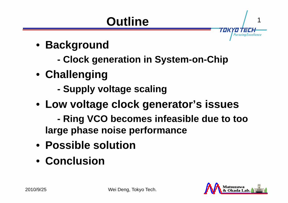
1Outline
• Background- Clock generation in System-on-Chip
• Challengingg g- Supply voltage scaling
L lt l k t ’ i• Low voltage clock generator’s issues- Ring VCO becomes infeasible due to too
large phase noise performance• Possible solutionPossible solution• Conclusion
Matsuzawa& Okada Lab.Matsuzawa& Okada Lab.2010/9/25 Wei Deng, Tokyo Tech.
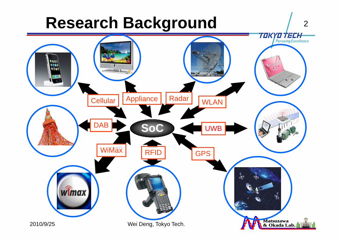
2Research Background
WLANCellular RadarAppliance
DAB 4UWBSoC
RFID GPSWiMax
Matsuzawa& Okada Lab.Matsuzawa& Okada Lab.2010/9/25 Wei Deng, Tokyo Tech.
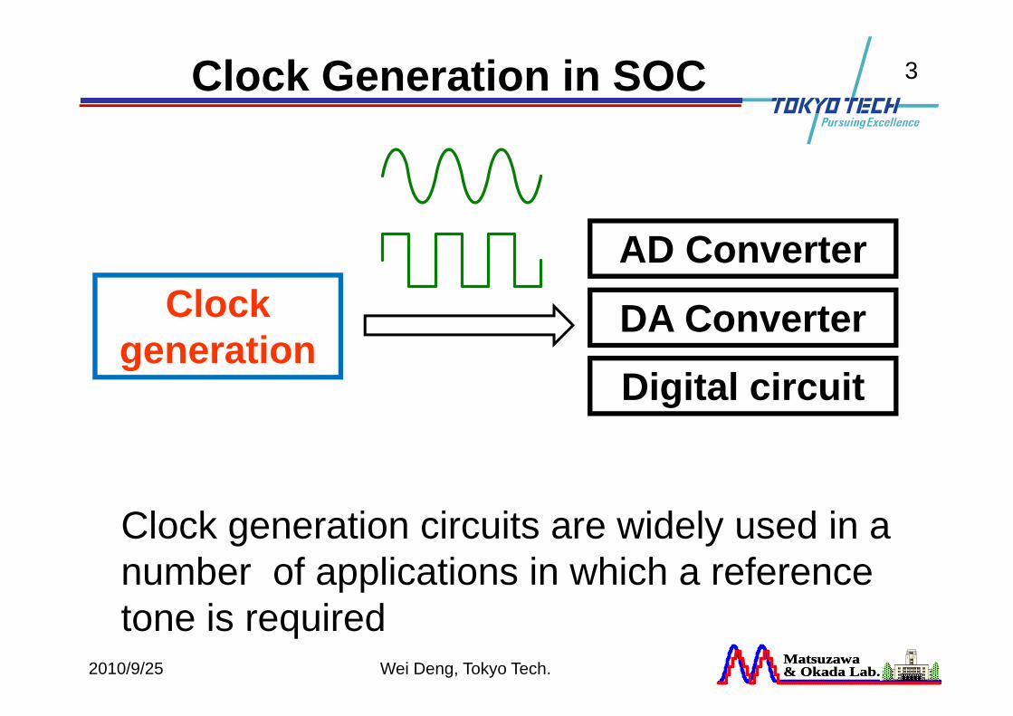
3Clock Generation in SOC
AD ConverterClock
generationDA Converter
generationDigital circuit
Clock generation circuits are widely used in aClock generation circuits are widely used in a number of applications in which a reference
Matsuzawa& Okada Lab.Matsuzawa& Okada Lab.2010/9/25
tone is requiredWei Deng, Tokyo Tech.
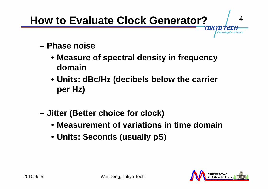
4How to Evaluate Clock Generator?
– Phase noise • Measure of spectral density in frequency
domain• Units: dBc/Hz (decibels below the carrier
per Hz)
– Jitter (Better choice for clock)( )• Measurement of variations in time domain• Units: Seconds (usually pS)• Units: Seconds (usually pS)
Matsuzawa& Okada Lab.Matsuzawa& Okada Lab.2010/9/25 Wei Deng, Tokyo Tech.
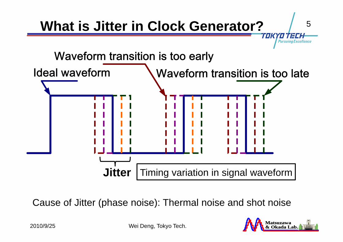
5What is Jitter in Clock Generator?
Jitter Timing variation in signal waveform
Cause of Jitter (phase noise): Thermal noise and shot noise
Jitter g g
Matsuzawa& Okada Lab.Matsuzawa& Okada Lab.2010/9/25 Wei Deng, Tokyo Tech.
Cause of Jitter (phase noise): Thermal noise and shot noise
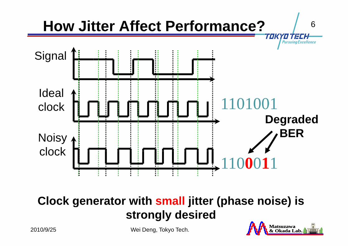
6How Jitter Affect Performance?
Signal
IdealIdeal clock 1101001
DegradedNoisy clock
Degraded BER
clock1100011
Clock generator with small jitter (phase noise) is
Matsuzawa& Okada Lab.Matsuzawa& Okada Lab.
g j (p )strongly desired
2010/9/25 Wei Deng, Tokyo Tech.
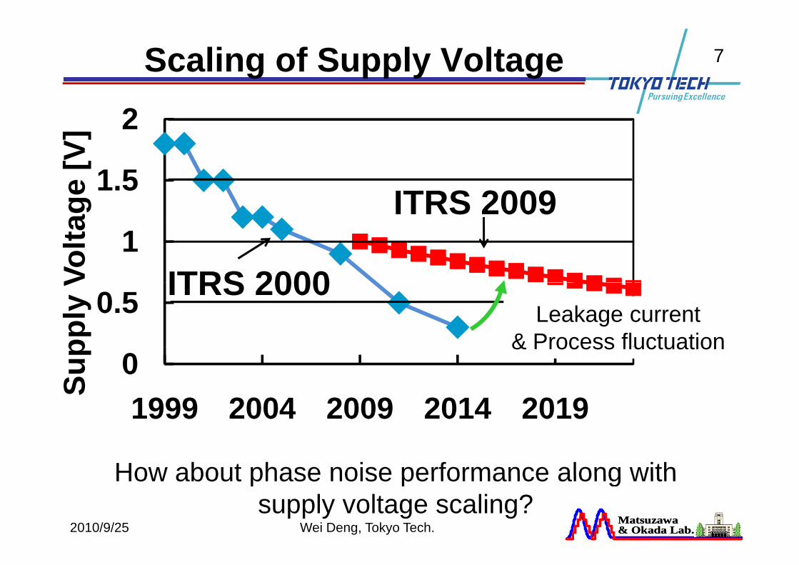
7Scaling of Supply Voltage2
V]
1.5
age
[V
ITRS 20091
Volta
ITRS 20000.5
pply
V
Leakage current& Process fluctuation
ITRS 2000
01999 2004 2009 2014 2019
Sup & Process fluctuation
1999 2004 2009 2014 2019
How about phase noise performance along withMatsuzawa& Okada Lab.Matsuzawa& Okada Lab.2010/9/25 Wei Deng, Tokyo Tech.
How about phase noise performance along with supply voltage scaling?
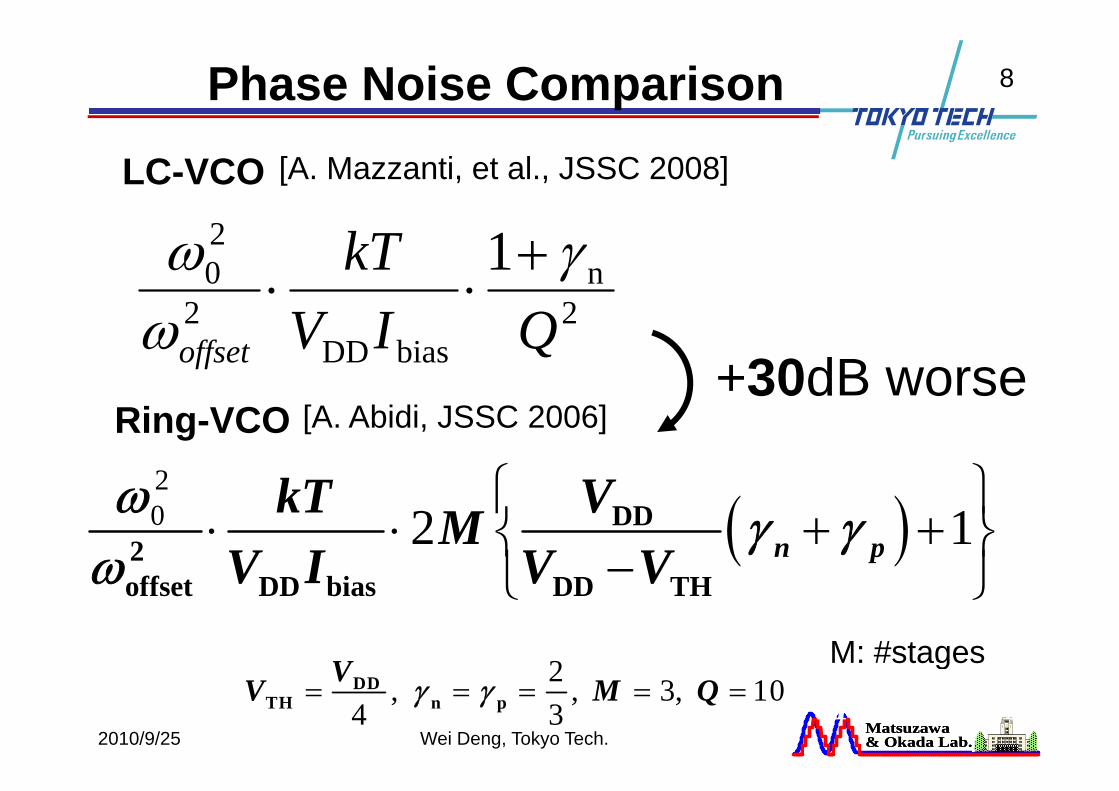
8Phase Noise Comparison
LC-VCO [A. Mazzanti, et al., JSSC 2008]
20 1 nkTω γ+⋅ ⋅ 2
n2
20 1kT γω +
⋅⋅2 2offset DD biasV I Qω
⋅ ⋅
+30dB worse2
biasDD2 QIVoffsetω
Ring-VCO30d o se
[A. Abidi, JSSC 2006]
2 VkT ⎧ ⎫( )20 2 1DD
2 n pVkT M
V I V Vω γ γω
⎧ ⎫⋅ ⋅ + +⎨ ⎬−⎩ ⎭
M: #stages2V
offset DD bias DD THV I V Vω ⎩ ⎭
Matsuzawa& Okada Lab.Matsuzawa& Okada Lab.
g2, , 3, 10
4 3= = = = =DD
TH n pVV M Qγ γ2, , 3, 10
4 3DD
TH n p VV M Qγ γ= = = = =2010/9/25 Wei Deng, Tokyo Tech.
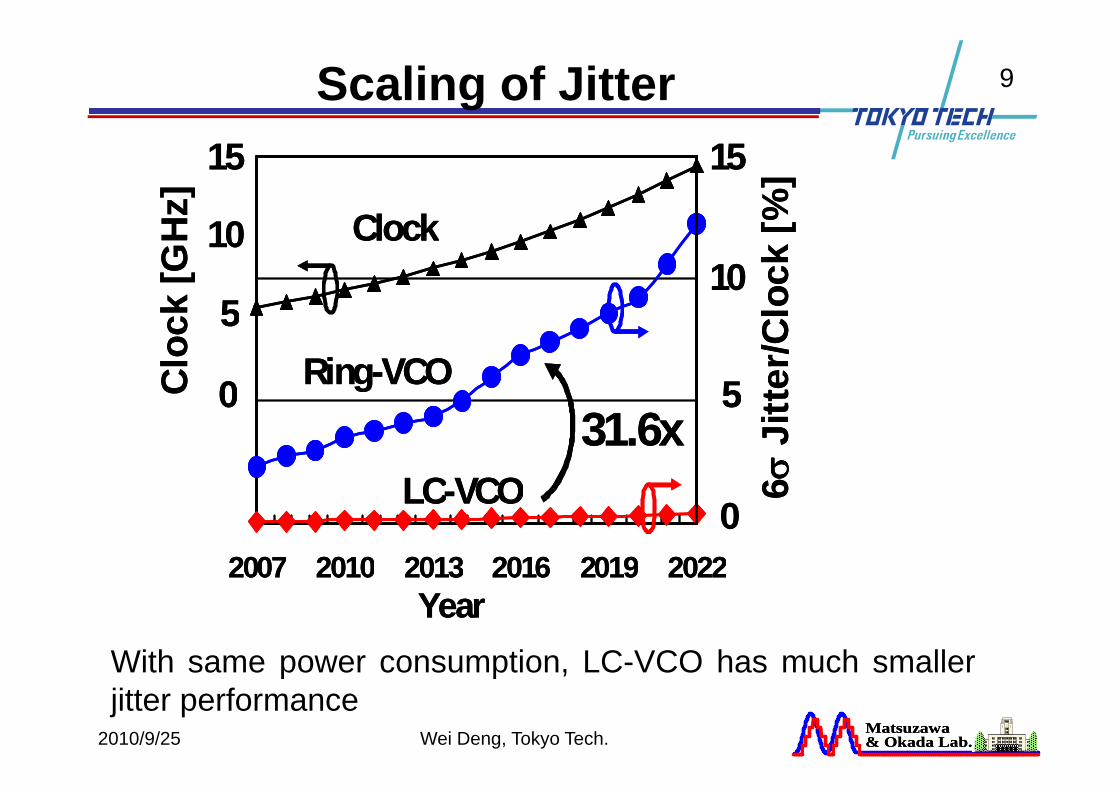
9Scaling of Jitter15
Cl k %]
z]15 15
Cl k %]
z]15
10Clock
ock
[%
k [G
H 10
510
Clock
ock
[%
k [G
H 10
5Ring-VCO 5 te
r/Clo
Clo
ck 5
0 Ring-VCO 5 ter/C
lo
Clo
ck 5
0
LC VCO31.6x
5
6σJi
tt0
LC VCO31.6x
5
6σJi
tt0
2007 2010 2013 2016 2019 2022
LC-VCO 0
6
2007 2010 2013 2016 2019 2022
LC-VCO 0
6
2007 2010 2013 2016 2019 2022Year
2007 2010 2013 2016 2019 2022Year
With same power consumption LC-VCO has much smaller
Matsuzawa& Okada Lab.Matsuzawa& Okada Lab.2010/9/25 Wei Deng, Tokyo Tech.
With same power consumption, LC-VCO has much smallerjitter performance
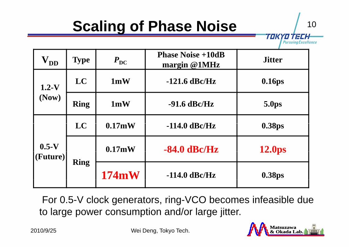
10Scaling of Phase Noise
VDD Type PDCPhase Noise +10dB
margin @1MHz Jitterg @
1.2-V(N )
LC 1mW -121.6 dBc/Hz 0.16ps
(Now)Ring 1mW -91.6 dBc/Hz 5.0ps
LC 0 17 W 114 0 dB /H 0 38
0.5-V
LC 0.17mW -114.0 dBc/Hz 0.38ps
0.17mW -84.0 dBc/Hz 12.0ps(Future)
Ring0.17mW 84.0 dBc/Hz 12.0ps
174mW -114.0 dBc/Hz 0.38ps
For 0.5-V clock generators, ring-VCO becomes infeasible due
Matsuzawa& Okada Lab.Matsuzawa& Okada Lab.2010/9/25 Wei Deng, Tokyo Tech.
to large power consumption and/or large jitter.
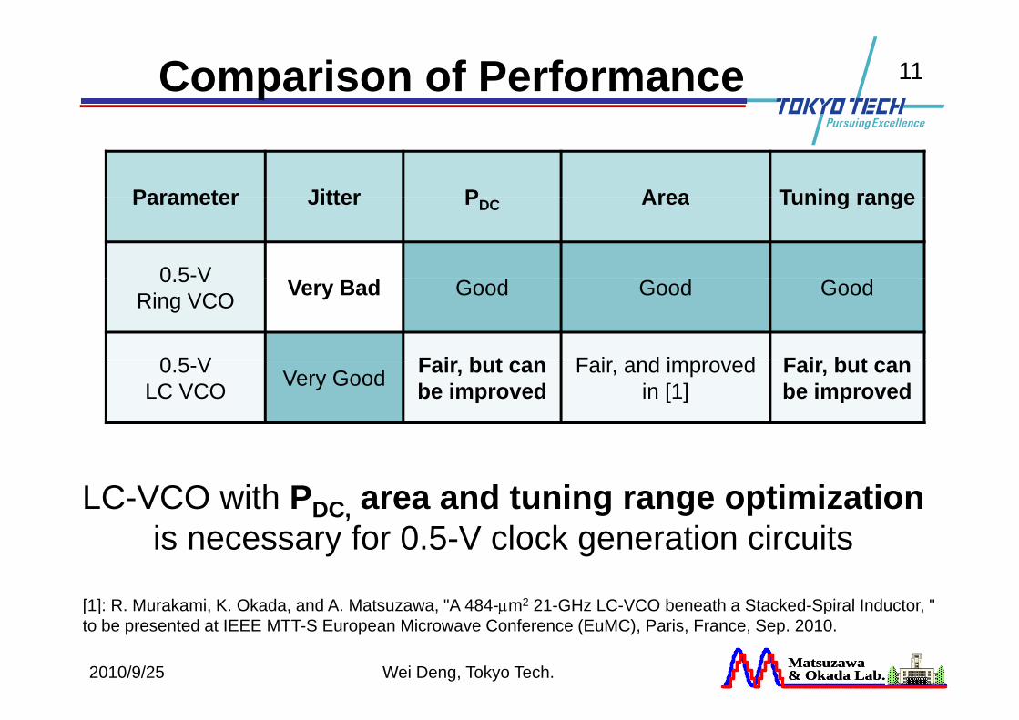
11Comparison of Performance
Parameter Jitter P Area Tuning rangeParameter Jitter PDC Area Tuning range
0 5-V0.5 VRing VCO Very Bad Good Good Good
0 5 V F i b t F i d i d F i b t0.5-VLC VCO Very Good Fair, but can
be improvedFair, and improved
in [1]Fair, but can be improved
LC-VCO with PDC, area and tuning range optimization
[1]: R Murakami K Okada and A Matsuzawa "A 484 μm2 21 GHz LC VCO beneath a Stacked Spiral Inductor "
is necessary for 0.5-V clock generation circuits
Matsuzawa& Okada Lab.Matsuzawa& Okada Lab.2010/9/25 Wei Deng, Tokyo Tech.
[1]: R. Murakami, K. Okada, and A. Matsuzawa, A 484-μm2 21-GHz LC-VCO beneath a Stacked-Spiral Inductor, to be presented at IEEE MTT-S European Microwave Conference (EuMC), Paris, France, Sep. 2010.
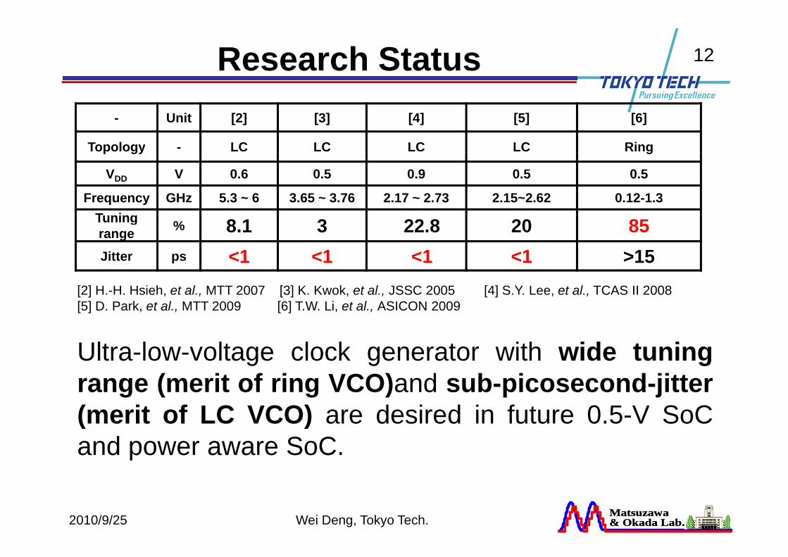
12Research Status- Unit [2] [3] [4] [5] [6]
Topology - LC LC LC LC Ringp gy g
VDD V 0.6 0.5 0.9 0.5 0.5
Frequency GHz 5.3 ~ 6 3.65 ~ 3.76 2.17 ~ 2.73 2.15~2.62 0.12-1.3T ningTuning range % 8.1 3 22.8 20 85Jitter ps <1 <1 <1 <1 >15
[2] H.-H. Hsieh, et al., MTT 2007 [3] K. Kwok, et al., JSSC 2005 [4] S.Y. Lee, et al., TCAS II 2008 [5] D. Park, et al., MTT 2009 [6] T.W. Li, et al., ASICON 2009
Ul l l l k i h id iUltra-low-voltage clock generator with wide tuningrange (merit of ring VCO)and sub-picosecond-jitter( i f LC VCO) d i d i f 0 5 V S C(merit of LC VCO) are desired in future 0.5-V SoCand power aware SoC.
Matsuzawa& Okada Lab.Matsuzawa& Okada Lab.2010/9/25 Wei Deng, Tokyo Tech.
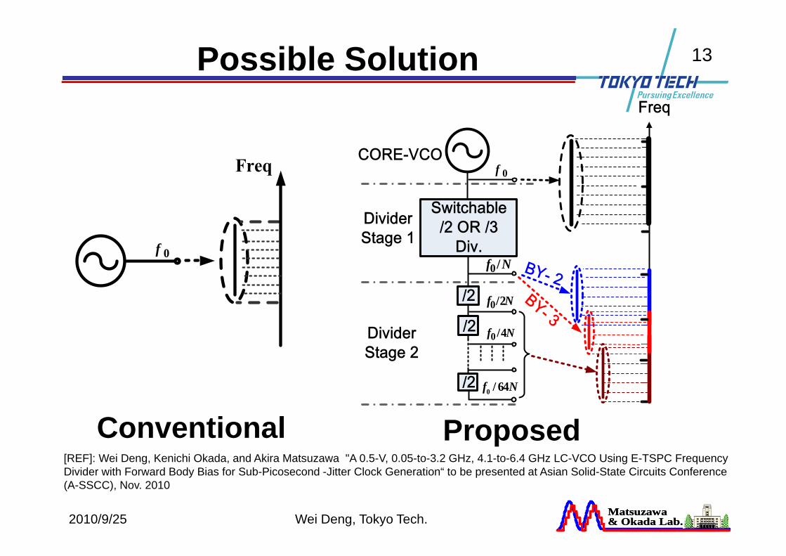
13Possible Solution
0f
Nf /00f
Nf 2/0
Nf 4/0
0 / 64f N
Conventional Proposed[REF]: Wei Deng, Kenichi Okada, and Akira Matsuzawa "A 0.5-V, 0.05-to-3.2 GHz, 4.1-to-6.4 GHz LC-VCO Using E-TSPC Frequency Di id i h F d B d Bi f S b Pi d Ji Cl k G i “ b d A i S lid S Ci i C f
Matsuzawa& Okada Lab.Matsuzawa& Okada Lab.2010/9/25 Wei Deng, Tokyo Tech.
Divider with Forward Body Bias for Sub-Picosecond -Jitter Clock Generation“ to be presented at Asian Solid-State Circuits Conference (A-SSCC), Nov. 2010
14Summary
• Lowering of supply voltage is required to realize g pp y g qlow-active-power circuits.
• Phase noise (Jitter) will become larger according toPhase noise (Jitter) will become larger according to the voltage scaling.
• Ring VCO become infeasible due to too large• Ring-VCO become infeasible due to too large phase noise (jitter) and/or too large power consumptionconsumption.
• To reduce the power consumption of the clock generator adoption of LC VCOs is an na oidablegenerator, adoption of LC-VCOs is an unavoidable way in such low-voltage condition.
Matsuzawa& Okada Lab.Matsuzawa& Okada Lab.2010/9/25 Wei Deng, Tokyo Tech.
15Toward the Future
• Ultra-low-voltage LC-VCO offers tremendousopportunities in phase noise (jitter) performanceopportunities in phase noise (jitter) performanceof clock generator in SoC design.
• The tuning range of ultra-low-voltage LC-VCOshould be improved to fulfill the requirement forfuture 0.5-V sub-picosecond-jitter clockgeneration.
Matsuzawa& Okada Lab.Matsuzawa& Okada Lab.2010/9/25 Wei Deng, Tokyo Tech.
16
Thanks for your attention!y
Q & A
Matsuzawa& Okada Lab.Matsuzawa& Okada Lab.2010/9/25 Wei Deng, Tokyo Tech.