Embed Size (px)
Citation preview
© 2009 IEEE International Solid-State Circuits Conference © 2009 IEEE1
A 2.2GHz 7.6mW Sub-Sampling PLL with -126dBc/Hz In-band Phase Noise and
0.15psrms Jitter in 0.18μm CMOS
Xiang Gao, Eric Klumperink, Mounir Bohsali*, and Bram Nauta
University of Twente, The Netherlands* National Semiconductor, California
© 2009 IEEE International Solid-State Circuits Conference © 2009 IEEE2
• PLL Noise Analysis
• Sub-sampling PLL
• Experimental Results
• Benchmark
• Conclusion
Outline
© 2009 IEEE International Solid-State Circuits Conference © 2009 IEEE3
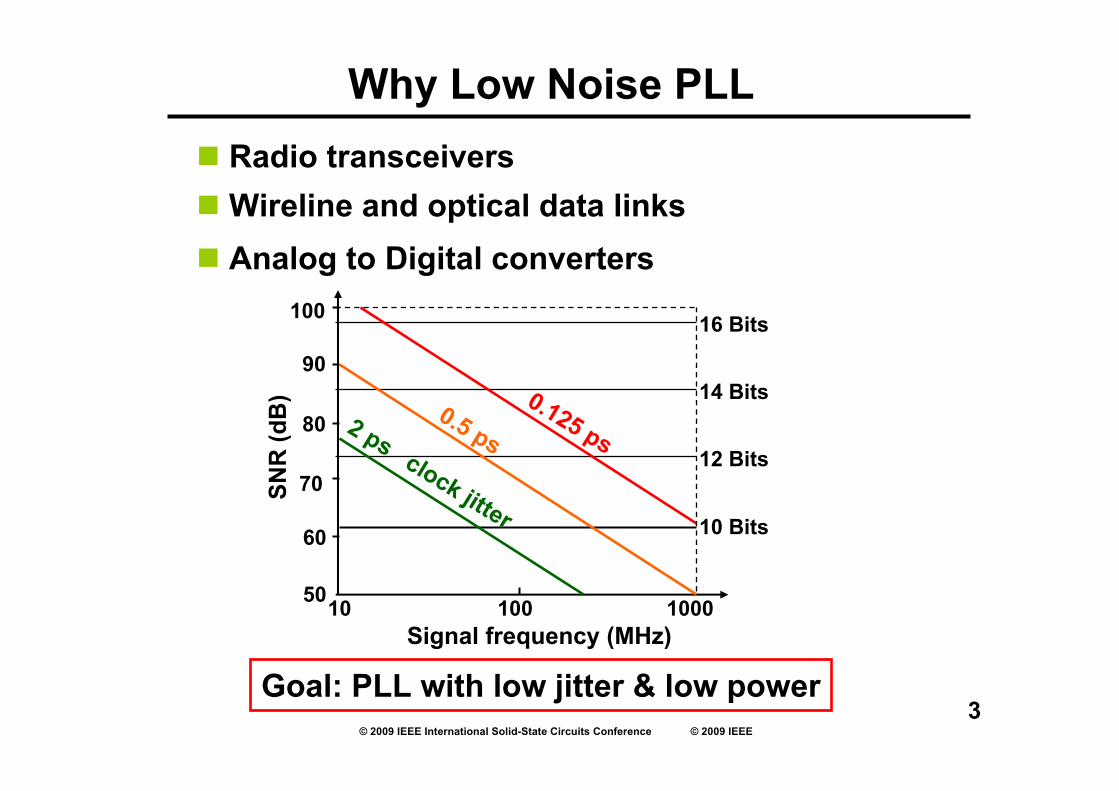
Why Low Noise PLL
Wireline and optical data links Radio transceivers
Analog to Digital converters
16 Bits
14 Bits
12 Bits
10 Bits
10 100 1000Signal frequency (MHz)
100
90
80
SNR
(dB
)
70
60
50
2 psclock jitter
0.5 ps
0.125 ps
Goal: PLL with low jitter & low power
© 2009 IEEE International Solid-State Circuits Conference © 2009 IEEE4
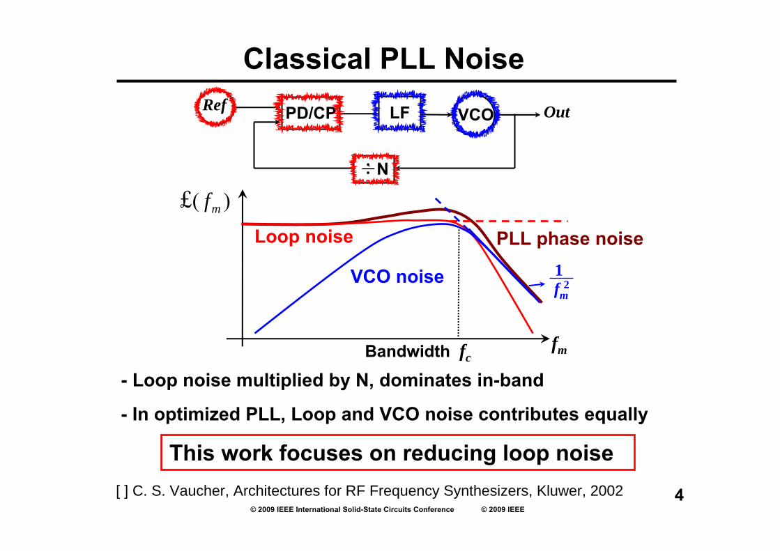
Classical PLL Noise
÷N
PD/CPRef OutVCOLF
- Loop noise multiplied by N, dominates in-band
PLL phase noise
fm
)(£ mf
Bandwidth fc
Loop noise
VCO noise 21fm
This work focuses on reducing loop noise[ ] C. S. Vaucher, Architectures for RF Frequency Synthesizers, Kluwer, 2002
- In optimized PLL, Loop and VCO noise contributes equally
© 2009 IEEE International Solid-State Circuits Conference © 2009 IEEE5
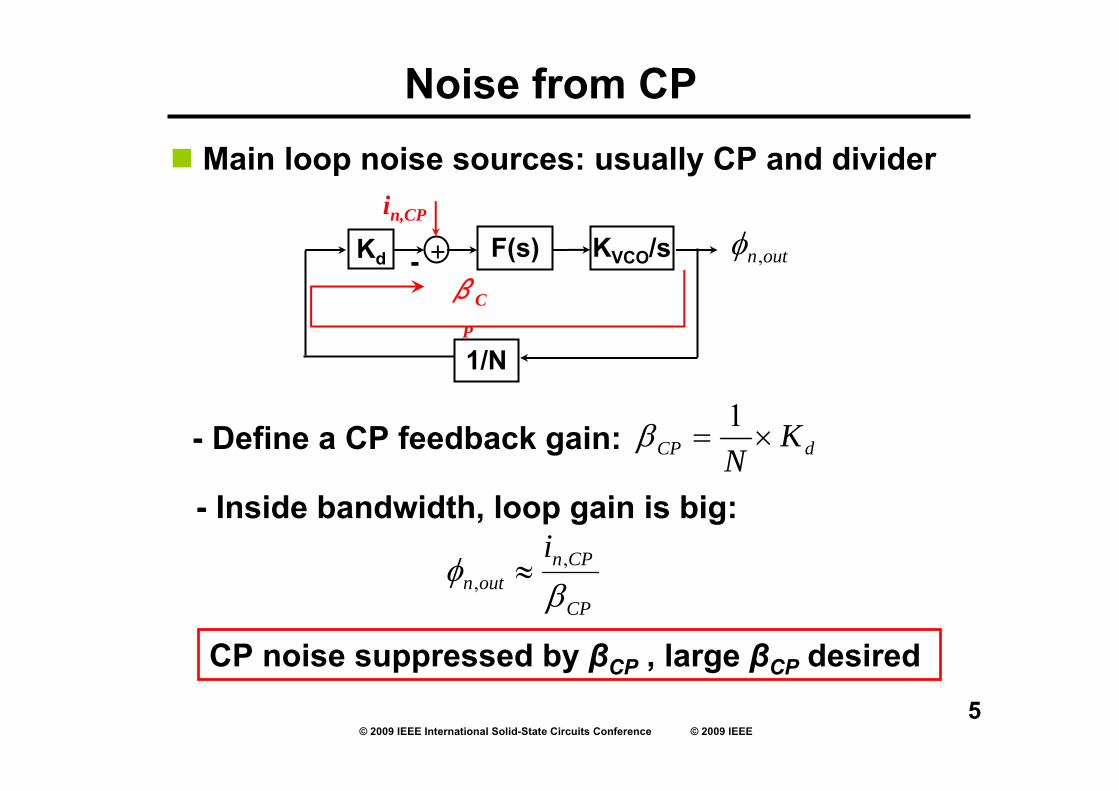
CP
CPnoutn
iβ
φ ,, ≈
- Define a CP feedback gain:
Main loop noise sources: usually CP and divider
Noise from CP
dCP KN×=
1β
-Kd F(s) KVCO/s
1/N
+
in,CP
outn,φβC
P
CP noise suppressed by βCP , large βCP desired
- Inside bandwidth, loop gain is big:
© 2009 IEEE International Solid-State Circuits Conference © 2009 IEEE6
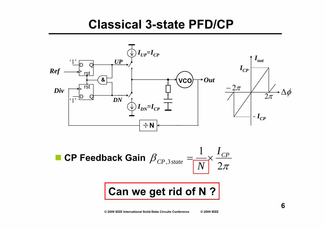
Classical 3-state PFD/CP
πβ
21
3CP
stateCPI
N×=,
‘1’
D Qrst
‘1’Ref
Div&
UP
DN
rst
D Q
CP Feedback Gain
IUP=ICP
IDN=ICP
÷N
OutVCOπ2−
π2
ICP
Iout
φΔ
- ICP
Can we get rid of N ?
© 2009 IEEE International Solid-State Circuits Conference © 2009 IEEE7
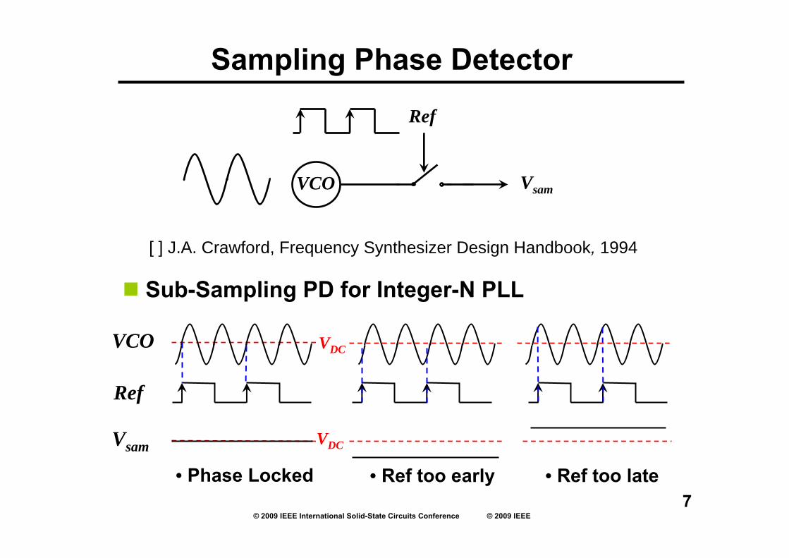
Sampling Phase Detector
• Ref too early • Ref too late
Sub-Sampling PD for Integer-N PLL
[ ] J.A. Crawford, Frequency Synthesizer Design Handbook, 1994
VCO
Ref
Vsam
• Phase Locked
VDC
VDC
VCO
Ref
Vsam
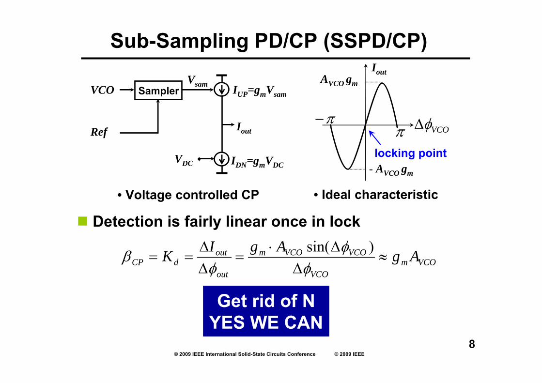
© 2009 IEEE International Solid-State Circuits Conference © 2009 IEEE8
SamplerVsamVCO
Ref
IUP=gmVsam
IDN=gmVDCVDC
Ioutπ−
π
AVCO gm
Iout
VCOφΔ
- AVCO gm
VCOmVCO
VCOVCOm
out
outdCP AgAgIK ≈
ΔΔ⋅
=ΔΔ
==φ
φφ
β )sin(
Sub-Sampling PD/CP (SSPD/CP)
• Voltage controlled CP • Ideal characteristic
Detection is fairly linear once in lock
locking point
Get rid of NYES WE CAN
© 2009 IEEE International Solid-State Circuits Conference © 2009 IEEE9
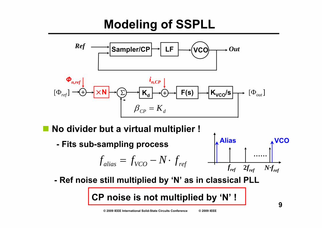
Modeling of SSPLL
- Fits sub-sampling process
No divider but a virtual multiplier !
refVCOalias fNff ⋅−=
Sampler/CP VCORef OutLF
Φn,ref in,CP
N ∑-
Kd F(s) KVCO/s [Фout ]+[Фref ] +
dCP K=β
CP noise is not multiplied by ‘N’ !
- Ref noise still multiplied by ‘N’ as in classical PLLfref 2fref
……
N·fref
VCOAlias
© 2009 IEEE International Solid-State Circuits Conference © 2009 IEEE10
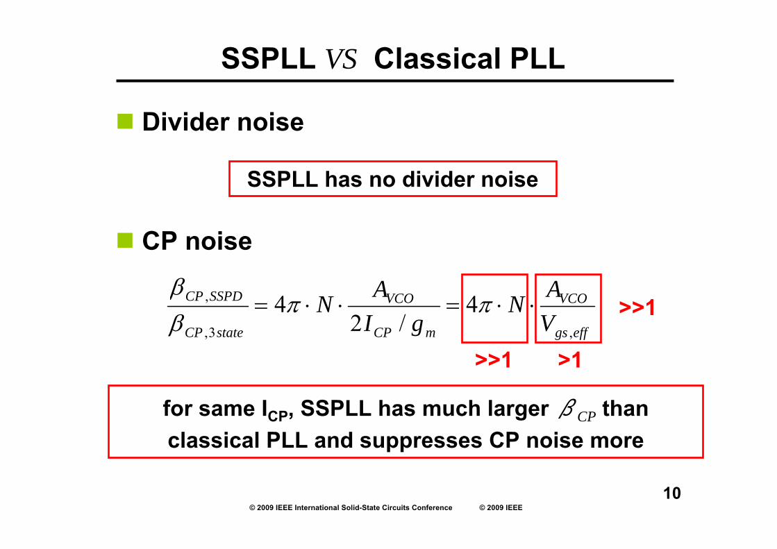
effgs
VCO
mCP
VCO
stateCP
SSPDCP
VAN
gIAN
,,
,
/⋅⋅=⋅⋅= ππ
ββ
42
43
SSPLL VS Classical PLL
for same ICP, SSPLL has much larger βCP than classical PLL and suppresses CP noise more
CP noise
>1>>1
>>1
Divider noise
SSPLL has no divider noise
© 2009 IEEE International Solid-State Circuits Conference © 2009 IEEE11
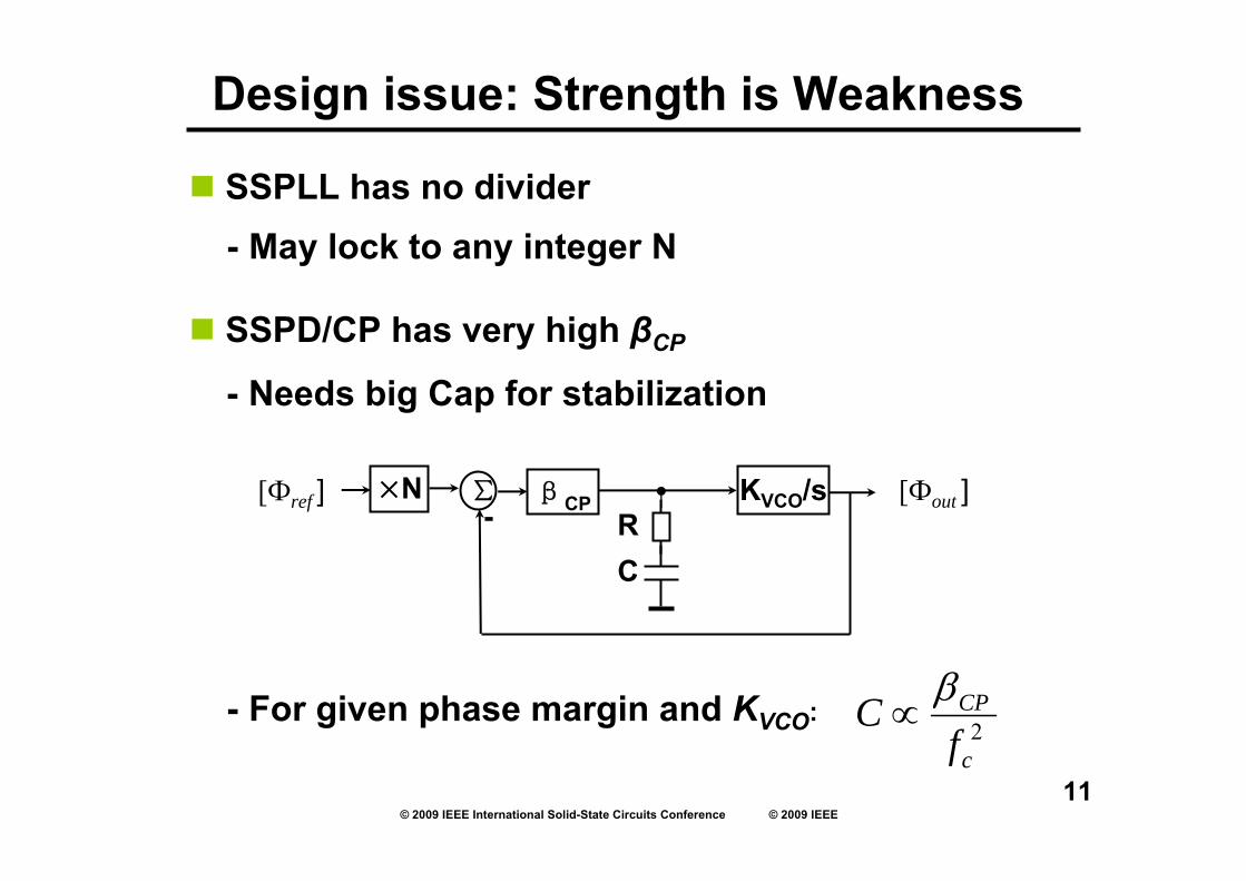
Design issue: Strength is Weakness
- Needs big Cap for stabilization
2c
CP
fC β∝
SSPD/CP has very high βCP
SSPLL has no divider
N ∑-
βCP KVCO/s [Фout ][Фref ]RC
- May lock to any integer N
- For given phase margin and KVCO:
© 2009 IEEE International Solid-State Circuits Conference © 2009 IEEE12
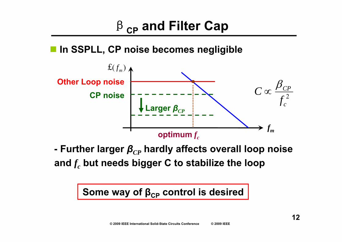
βCP and Filter Cap
- Further larger βCP hardly affects overall loop noise and fc but needs bigger C to stabilize the loop
In SSPLL, CP noise becomes negligible
CP noiseOther Loop noise
fm
Larger βCP
Some way of βCP control is desired
2c
CP
fC β∝
optimum fc
)(£ mf
© 2009 IEEE International Solid-State Circuits Conference © 2009 IEEE13
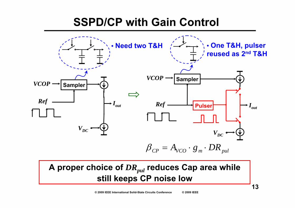
SSPD/CP with Gain Control
A proper choice of DRpul reduces Cap area while still keeps CP noise low
pulmVCOCP DRgA ⋅⋅=β
Ref
VCOP Sampler
VDC
Iout
Sampler
Ref Pulser
VCOP
VDC
Iout
• One T&H, pulserreused as 2nd T&H
• Need two T&H
© 2009 IEEE International Solid-State Circuits Conference © 2009 IEEE14
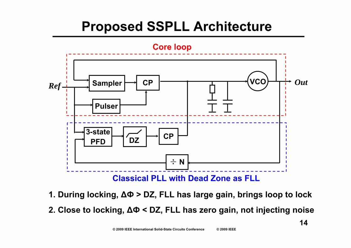
Ref Out
Classical PLL with Dead Zone as FLL
Sampler VCOCP
Pulser
3-statePFD
÷ N
CPDZ
Proposed SSPLL Architecture
1. During locking, ∆Ф > DZ, FLL has large gain, brings loop to lock
2. Close to locking, ∆Ф < DZ, FLL has zero gain, not injecting noise
Core loop
© 2009 IEEE International Solid-State Circuits Conference © 2009 IEEE15
Vtune
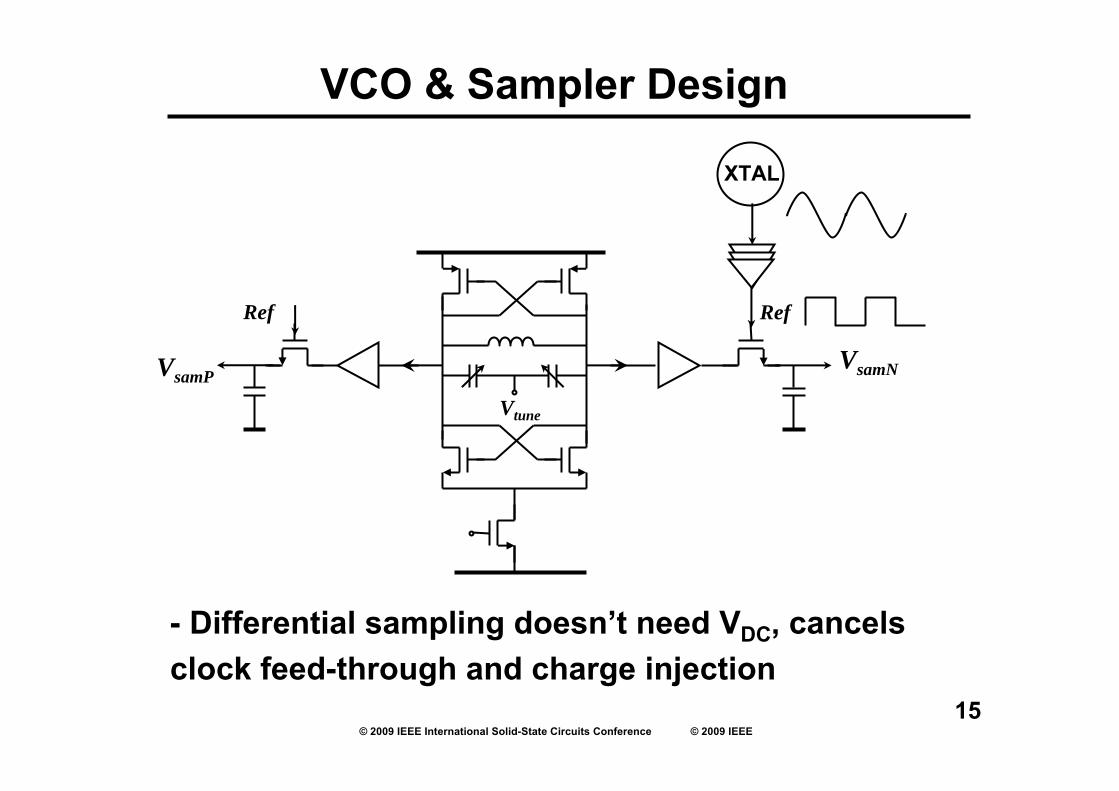
VCO & Sampler Design
Ref
VsamPVsamN
Ref
XTAL
- Differential sampling doesn’t need VDC, cancels clock feed-through and charge injection
© 2009 IEEE International Solid-State Circuits Conference © 2009 IEEE16
Pul
PulPul
Iout
VsamP VsamN
Pul
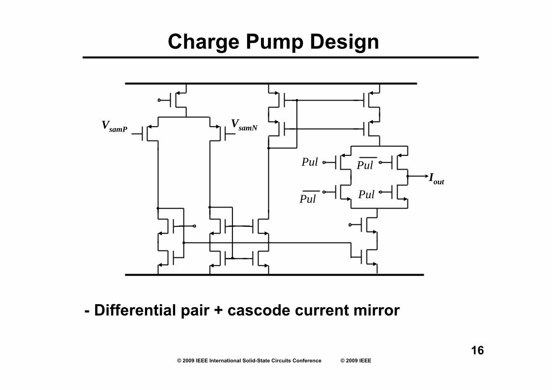
Charge Pump Design
- Differential pair + cascode current mirror
© 2009 IEEE International Solid-State Circuits Conference © 2009 IEEE17
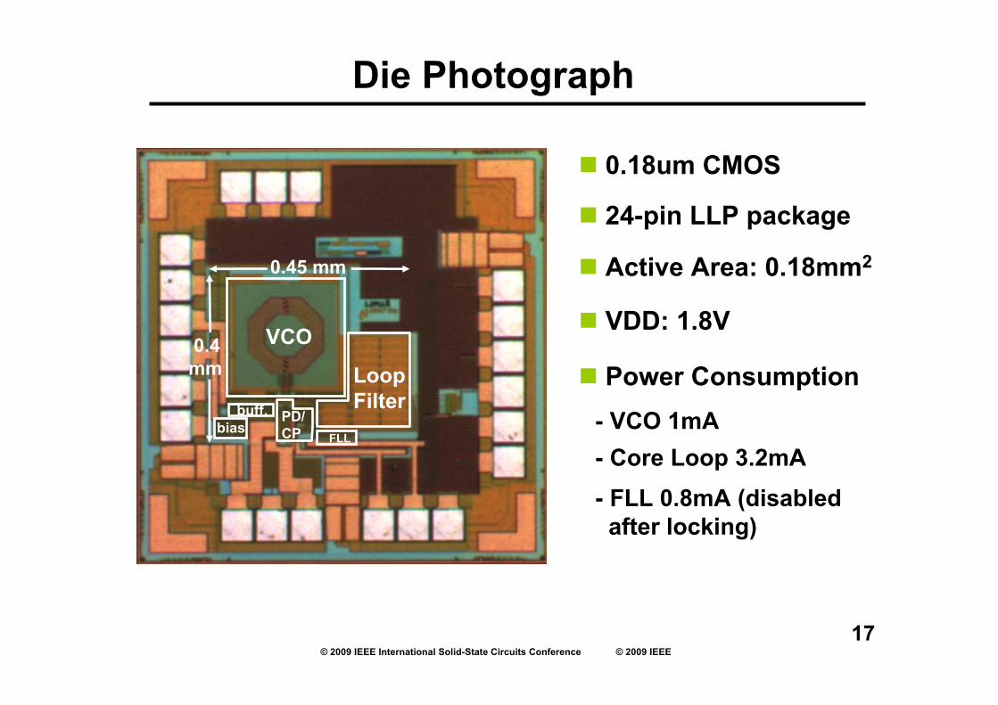
Die Photograph
0.18um CMOS
Active Area: 0.18mm2
VDD: 1.8V
- VCO 1mA
VCO
50Ω buf.bias
CP
LoopFilter
FLL
PD,b
uf.
FLL
0.4mm
0.45 mm
pul.
VCO
buff.bias
LoopFilter
FLL
0.4mm
0.45 mm
PD/CP
- FLL 0.8mA (disabledafter locking)
- Core Loop 3.2mA
Power Consumption
24-pin LLP package
© 2009 IEEE International Solid-State Circuits Conference © 2009 IEEE18
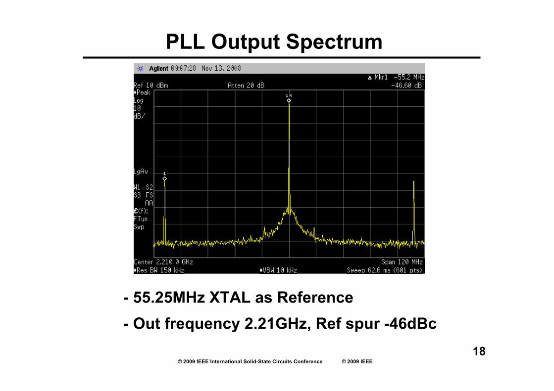
PLL Output Spectrum
- Out frequency 2.21GHz, Ref spur -46dBc- 55.25MHz XTAL as Reference
© 2009 IEEE International Solid-State Circuits Conference © 2009 IEEE19
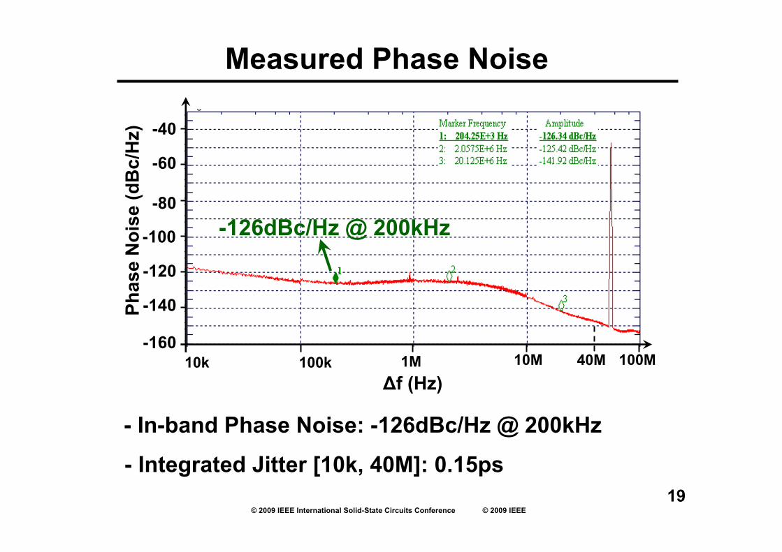
Measured Phase Noise
- In-band Phase Noise: -126dBc/Hz @ 200kHz
- Integrated Jitter [10k, 40M]: 0.15ps
10k
-60
-80
-100
-120
-140
-160
-40
100k 1M 10M 100M
Phas
e N
oise
(dB
c/H
z)
∆f (Hz)40M
-126dBc/Hz @ 200kHz
© 2009 IEEE International Solid-State Circuits Conference © 2009 IEEE20
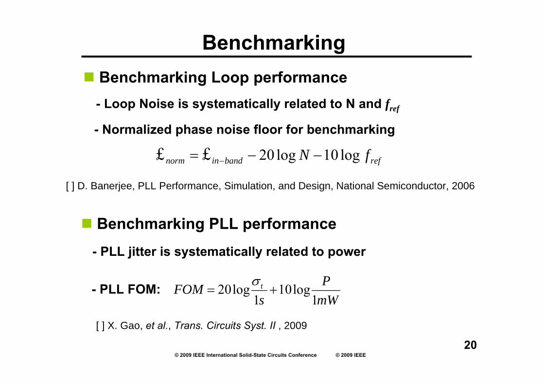
Benchmarking
- Normalized phase noise floor for benchmarking
refbandinnorm fN loglog££ 1020 −−= −
- Loop Noise is systematically related to N and fref
Benchmarking Loop performance
Benchmarking PLL performance
mWP
sFOM t
110
120 loglog +=
σ
- PLL jitter is systematically related to power
- PLL FOM:
[ ] D. Banerjee, PLL Performance, Simulation, and Design, National Semiconductor, 2006
[ ] X. Gao, et al., Trans. Circuits Syst. II , 2009
© 2009 IEEE International Solid-State Circuits Conference © 2009 IEEE21
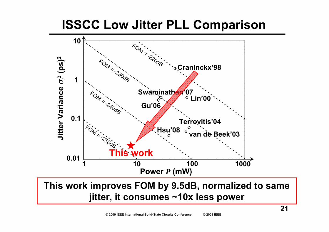
2
Swaminathan’07
Gu’06Lin’00
Craninckx’98
FOM = -220dBFOM = -230dB
FOM = -240dB
Hsu’08Terrovitis’04
van de Beek’03FOM = -250dB
This work
Power P (mW)
Jitte
r Var
ianc
e σ t
2(p
s)2
ISSCC Low Jitter PLL Comparison
This work improves FOM by 9.5dB, normalized to same jitter, it consumes ~10x less power
1
0.1
0.01
10
1 10 100 1000
© 2009 IEEE International Solid-State Circuits Conference © 2009 IEEE22
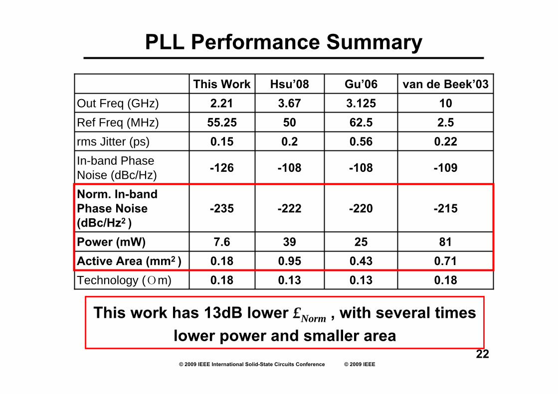
0.180.187.6
-235
-126
0.1555.25 2.21
This Work
0.130.9539
-222
-108
0.250
3.67 Hsu’08
0.130.4325
-220
-108
0.5662.5 3.125Gu’06
0.18Technology (Оm)0.71Active Area (mm2 )81Power (mW)
-215Norm. In-band Phase Noise (dBc/Hz2 )
-109In-band Phase Noise (dBc/Hz)
0.22rms Jitter (ps)2.5 Ref Freq (MHz)10 Out Freq (GHz)
van de Beek’03
PLL Performance Summary
This work has 13dB lower £Norm , with several times lower power and smaller area
© 2009 IEEE International Solid-State Circuits Conference © 2009 IEEE23
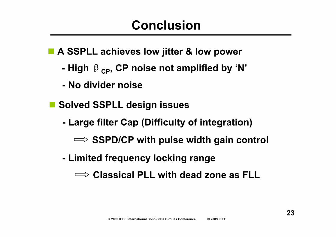
Conclusion
- High βCP, CP noise not amplified by ‘N’
- No divider noise
A SSPLL achieves low jitter & low power
- Large filter Cap (Difficulty of integration)
- Limited frequency locking range
Solved SSPLL design issues
SSPD/CP with pulse width gain control
Classical PLL with dead zone as FLL
© 2009 IEEE International Solid-State Circuits Conference © 2009 IEEE24
Acknowledgement
The authors wish to thank
- Ali Djabbari, Jerry Socci and Kim Yeow Wong for useful discussions
- Glen Wells for layout assistance
- Gerard Wienk and Henk de Vries for practicalassistance


![EC0804-PLL [Modo de compatibilidad]€¦ · (PLL) 1 Capítulo 4 Lazos enganchados en fase. PLL Aplicaciones de los PLL Síntesis de frecuencia Partiendo de un oscilador patrón (f0),](https://img.pdfslide.tips/doc/110x75/5e8e438d8741af3761030a0b/ec0804-pll-modo-de-compatibilidad-pll-1-captulo-4-lazos-enganchados-en-fase.jpg)