Embed Size (px)
Citation preview

Valery Vodovozov Raik Jansikene
POWER ELECTRONIC CONVERTERS
www.IranSwitching.ir

Vodovozov, Valery, Jansikene, Raik. Power Electronic Converters. 2006.
Valery Vodovozov has a PhD Degree in Electrical Engineering from St. Pe-tersburg Electrotechnical University, Russia, where he works since 1976 as associated professor and senior researcher. His teaching includes electric drives, computer science, electronics, and programming of electromechani-cal, electronics, and human informational systems. The scientific interests and major fields of research include applying object oriented technologies in industry and education.
In addition to Electrical Engineering University, he teaches at St. Petersburg Institute for Ex-tra Professional Education and gives a number of courses on disciplines mentioned above in industrial and customs training centers. In 1997, 2002, and 2005 he worked as a visiting pro-fessor at Tallinn University of Technology, Estonia and in 2000 served in Scientific Research Laboratory of Ford Motor Company, USA. Professional associations include fellow of the Russian Society of Motor Drive Engineers, Estonian Society of M. H. Jacobi, and the Nordic Network for Electric Drives. He has been selected by International Biographical Center of Cambridge as International Man of the Years 1999 and 2000, included into Marquis "Whos Who in the World", "Whos Who in Sci-ence and Engineering" (1998-2005), "Famous Russians" (Moscow, Russia, 1999-2000) Valery Vodovozov is the author of books, inventions, brochures, and tutorials. More than 200 his publications appear in scientific journals and papers of international conferences. Among his monographs are Theory and Systems of Electric Drive (St. Petersburg: ETU, 2004), Programming Technique on VBA, Pascal, and C++ (St. Petersburg: ETU, 2001), Basics of Informational Technologies (Deaborn, USA: SRL, 2000), Practical Introduction to Informa-tional Systems (St. Petersburg: Polycom, 1995), Microprocessor CNC Systems (St. Pe-tersburg: Energoatomizdat, 1994), and Robots in Shipbuilding Manufactures (St. Peters-burg, Shipbuilding, 1986)
© 2006 Valery Vodovozov, Raik Jansikene
www.IranSwitching.ir

3
Contents
Designations.............................................................................................................................. 4 Abbreviations............................................................................................................................. 4 Preface ...................................................................................................................................... 5 Introduction................................................................................................................................ 6 Part 1. Rectifiers...................................................................................................................... 12
1.1. Common Features of Rectifiers............................................................................... 12 1.2. Single-Phase Half-Wave Rectifiers.......................................................................... 16 1.3. Single-Phase Full-Wave Rectifiers .......................................................................... 19 1.4. Single-Phase Bridge Rectifiers ................................................................................ 21 1.5. Three-Phase Full-Wave Rectifiers........................................................................... 23 1.6. Three-Phase Bridge Rectifiers................................................................................. 27
Part 2. Inverters....................................................................................................................... 31 2.1. Common Features of Inverters ................................................................................ 31 2.2. Voltage Source Inverters ......................................................................................... 35 2.3. Current Source Inverters.......................................................................................... 43 2.4. Resonant Inverters................................................................................................... 46
Part 3. AC/AC Converters ....................................................................................................... 49 3.1. AC Voltage Regulators ............................................................................................ 49 3.2. Direct Frequency Converters ................................................................................... 51 3.3. DC Link Converters.................................................................................................. 57
Part 4. DC/DC Converters....................................................................................................... 60 4.1. DC Voltage Regulators ............................................................................................ 60 4.2. Step-Down Choppers............................................................................................... 63 4.3. Step-Up Choppers ................................................................................................... 70 4.4. Universal Choppers.................................................................................................. 72
Part 5. Utility Circuits ............................................................................................................... 75 5.1. Snubbers and Clamps.............................................................................................. 75 5.2. Gate and Base Drivers............................................................................................. 79 5.3. Electromagnetic Compatibility ................................................................................. 84
Part 6. Experiments Using Electronics Workbench................................................................ 89 6.1. Objective .................................................................................................................. 89 6.2. Single-Phase Half-Wave Rectifiers.......................................................................... 90 6.3. Single-Phase Full-Wave Rectifiers .......................................................................... 92 6.4. Three-Phase Rectifiers ............................................................................................ 95 6.5. AC Converters.......................................................................................................... 96 6.6. Choppers .................................................................................................................. 99
Part 7. Questions................................................................................................................... 104 7.1. Test on Power Electronic Devices ......................................................................... 104 7.1. Test on Rectifiers ................................................................................................... 105 7.2. Test on Inverters .................................................................................................... 106 7.3. Test on AC/AC Converters .................................................................................... 107 7.4. Test on DC/DC Converters .................................................................................... 108 7.5. Test on Utility Circuits ............................................................................................ 108
Index...................................................................................................................................... 110 Standards .............................................................................................................................. 112 References ............................................................................................................................ 114
www.IranSwitching.ir

4
Designations
С capacitor D diode, thyristor L inductor, choke R resistor T transistor Z load w number of coils C capacitance cos ϕ power factor f frequency
K voltage gain I current m number of pulses L inductance LR load regulation P true power q duty cycle r ripple factor R resistance S apparent power
t time T period, cycle U voltage α firing angle β angle of advance γ commutation interval η efficiency ϕ phase angle ω angular frequency
Abbreviations
A Ampere ac alternating current B2 single-phase bridge rectifier B6 three-phase bridge rectifier BJT bipolar junction transistor CSI current source inverter dc direct current EMC electromagnetic compatibility EMI electromagnetic interference F Farad FET field-effect transistor G Giga = 109 (prefix) GTO gate turn-off thyristor H Henry HF high frequency Hz Hertz IGBT insulated gate bipolar transistor JFET junction FET k kilo = 103 (prefix) LF low frequency M Mega = 106 (prefix) m milli = 10-3 (prefix) M1 single-phase half-period rectifier
M2 single-phase midpoint rectifier M3 three-phase midpoint rectifier MOSFET metal-oxide semiconductor FET MCT MOS-controlled thyristor n nano = 10-9 (prefix) n negative p pico = 10-12 (prefix) p positive PIV peak inverse voltage PWM pulse-width modulation RFI radio frequency interference rms root mean square s second SCR silicon-controlled rectifier V Volt VSI voltage source inverter W Watt WA Volt-Ampere ZCS zero-current switch ZVS zero-voltage switch µ micro = 10-6 (prefix) Ω Ohm
www.IranSwitching.ir

5
Preface
The goal of this book is to introduce a reader to the basics of power electronic con-
verters. The emphasis is on the day-to-day electronic products. The course acquaints with the features and functions of rectifiers, inverters, ac/ac, and dc/dc converters. The content contains a wealth of technical information for students and practicing electrical engineers. It helps to learn the design of circuits and equipment based on electronic components.
The book is recommended for coming to know the discipline Introduction to Power Electron-ics. The problems discussed are: principles of electrical energy conversion; features of power electronic components; design and characteristics of power semiconductor convert-ers. The background of the course is Electronics and Semiconductor Engineering. After this course, students may learn to obtain a deeper knowledge of the advanced topics in power electronics. Usually, they need the theory that will offer an insight into the general op-eration of converter loading as well as the disturbances caused by variables, and possibili-ties for reducing these errors, partly in power devices with different kinds of loads. Such problems as the design and methods for implementing control equipment are not discussed deeply. Computer simulation instruments, modeling circuits, and analysis tools should be a subject of further interest for future engineers as well. The continuation of power electronics concerns the theory of generalized energy converter; control and protection of power elec-tronic circuits; problems of electromagnetic compatibility; selection of power electronic com-ponents for converters; control algorithms, programs, and microprocessor control devices of power electronic converters; cooling of power converters; power electronic system design. Authors thank the staff of Department of Electrical Drives and Power Electronics from Tallinn University of Technology for useful research and experimental information and for helpful recommendations that they got during the book preparing. Particular gratitude is expressed to Juhan Laugis, Tõnu Lehtla, Madis Lehtla, and Jury Joller whose materials have been used in the book. We strongly recommend their tutorials to everybody for going deep into the field. Nevertheless, larger the thematic of work, more drawbacks it includes. By understanding this obvious true, we thank beforehand everybody who will talk us any kinds of recalls, criticisms, and error messages. Please, send all to [email protected].
Authors
www.IranSwitching.ir

6
Introduction
Historical background. The earliest research in the field of power electronics has
been carried out since the end of the 19th century. In 1882, French physicist J. Jasmin has opened a phenomenon of semiconductance and proposed this effect to be used for rectify-ing alternating current instead of mechanical switches. In 1892, German researcher L. Arons has invented the first mercury arc vacuum valve. P.C. Hewitt developed the first arc valve in 1901 in US and a year later he patented the mercury rectifier. In 1906, J.A. Fleming has in-vented the first vacuum diode so far as an American electrician G.W. Pickard invented the silicon valve and L. Forest patented the vacuum tube. Electronic amplifiers development started with this invention and in 1907 a vacuum triode has been suggested by L. Forest. Later, on the basis of the same principles many kinds of electronic devices were worked out. Key of the technology was the invention of the feedback amplifier by H.S. Black in 1927. In 1921, F.W. Meyer from Germany first formulated the main principles and trends of power electronics. In the first half of the 20th century, electronic equipment was mainly based on vacuum tubes, such as gas-discharge valves, thyratrons, mercury arc rectifiers, and ignitrons. Until the end of twenties, vacuum diodes (kenotrones) were the main devices. In the thirties, they were replaced by more efficient mercury equipment. The majority of valves were arranged as co-axial closed cylinders round the cathode. More complex valves contained several gridded electrodes between the cathode and anode. By such a way, triode, tetrode, and pentode valves have been designed. The vacuum tube had a set of disadvantages. First, it had an internal power heater. Second, its life was limited by a few thousand hours before its filament burns out. Third, it takes up a lot of space. Fourth, it gave off heat that rises in internal temperature of the electronics equipment. Because of vacuum tube technology, the first electronic devices were very ex-pensive, bulky, and dissipated lots of power. The era of semiconductor devices began in 1947, when American scientists J. Bardeen, W.H. Brattain, and W.B. Shockley from Bell Labs have invented a germanium transistor. Later they were awarded a Nobel Prize for this invention. The advantages of a transistor overcome the disadvantages of the vacuum tube. From 1952, General Electric manufac-tured the first germanium diodes. In 1954, G. Teal at Texas Instruments has produced the silicon transistor, which gained wide commercial acceptance because of the increased tem-perature performance and reliability. During the mid 1950s through the early 1960s, elec-tronic circuit designs began to migrate from vacuum tubes to transistors, thereby opening up many new possibilities in research and development projects. The invention of the integrated circuit by J. Kilby from Texas Instruments in 1958 followed by the planar process of Fairchild Semiconductor in 1959, that became the key of solid-state electronics.
www.IranSwitching.ir

7
Before 1960s, semiconductor engineering was regarded as part of low-current and low-voltage electronic engineering. The currents used in solid-state devices were below one am-pere and voltages only a few tens of volts. The period of power semiconductors has began in 1956, when the silicon-based thyristors were invented by American research team lead by J. Moll. Based on these inventions, several generations of semiconductor devices have been worked out. The time of 1956 1975 can be considered as the era of the first generation power devices. During the years of second-generation power devices from 1975 till 1990, the metal-oxide semiconductor field-effect transistors, bipolar npn and pnp transistors, junc-tion transistors, and gate turn-off thyristors were developed. Later the microprocessors, specified integral circuits, and power integral circuits were produced. In the 1990s, the insu-lated gate bipolar transistor was established as the power switch of the third generation. A new trend in electronics became the use of intelligent power devices and intelligent power modules. Now, power electronics is a rapidly expanding field in electrical engineering and a scope of the technology covers a wide spectrum of electronic converters. Different kinds of power supplies are used everywhere in normal daily routines both at home, office work or in an in-dustrial environment. This is due to the progress in electronic components and equipment development that has been achieved in the last few decades. Electronic and electrical appa-ratus are everywhere, and all these devices need electrical power to work. Most of electronic supplies are switching semiconductor converters thanks to the efficiency, size, capability to operate at various current and voltage levels, control features and price compared to the lin-ear power supply. Power electronic system. Any technical system is an assembly of components that are connected together to form a functioning machine or operational procedure. A power elec-tronic system assembles the general building blocks:
• AC/DC converters rectifiers that convert ac to dc with adjustment of voltage and current;
• DC/AC converters inverters that produce ac of controllable magnitude and fre-quency, particularly with galvanic isolation via a transformer;
• AC/AC converters ac frequency, phase, magnitude, and power converters par-ticularly with an intermediary dc link;
• DC/DC converters linear regulators and switching choppers.
In turn, each block consists of the primary electronic elements that are: resistors, ca-pacitors, transformers, inductors (choke coils), frames, etc., and basic classes of semicon-ductor devices:
• diodes, including Zener, optoelectronic and Schottky diodes, and diacs; • thyristors, particularly silicon-controlled rectifiers (SCR), triacs, gate turn-off
(GTO), and MOS-controlled thyristors (MCT); • transistors, such as bipolar junction (BJT), field-effect (FET), and insulated gate
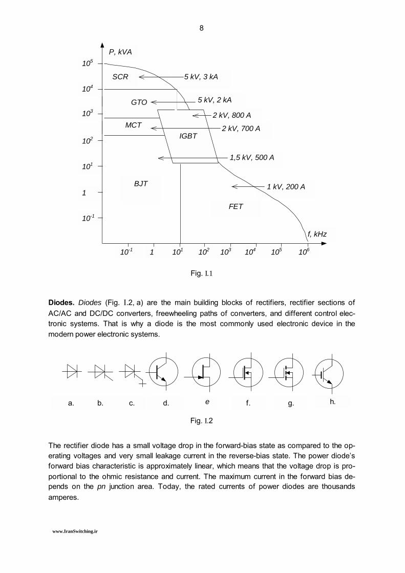
bipolar (IGBT) transistors. They are joined to control the load operation. The comparative diagram of power rat-
ing and switching speed of semiconductor electronic devices is given in Fig. I.1.
www.IranSwitching.ir
8
Fig. I.1
Diodes. Diodes (Fig. I.2, a) are the main building blocks of rectifiers, rectifier sections of AC/AC and DC/DC converters, freewheeling paths of converters, and different control elec-tronic systems. That is why a diode is the most commonly used electronic device in the modern power electronic systems.
Fig. I.2
The rectifier diode has a small voltage drop in the forward-bias state as compared to the op-erating voltages and very small leakage current in the reverse-bias state. The power diodes forward bias characteristic is approximately linear, which means that the voltage drop is pro-portional to the ohmic resistance and current. The maximum current in the forward bias de-pends on the pn junction area. Today, the rated currents of power diodes are thousands amperes.
1,5 kV, 500 A
5 kV, 2 kA
2 kV, 800 A
2 kV, 700 A
1 kV, 200 A
5 kV, 3 kA
f, kHz
MCT
GTO
10-1 1 101 102 103 104 105 106
104
103
102
101
1
10-1
105 P, kVA
BJT
IGBT
SCR
FET
с. a. b. d. g. f. h. e
www.IranSwitching.ir

9
At turn on, the diode can be considered as an ideal switch because it opens rapidly com-pared to transients in the circuit. In the most circuits, the leakage current does not affect sig-nificantly the circuit and so the diode can also be considered as switch. In case of reverse-biased voltage, only the small leakage current flows through the diode. This current is independent of the reverse voltage until the breakdown voltage is reached. After that, the diode voltage remains essentially constant while the current increases dra-matically. Only the resistance of the external circuit limits the maximum value of the current. Simultaneous large current and large voltage in the breakdown operation leads to excessive power dissipation that should quickly destroy the diode. Therefore, the breakdown operation of the diode must be avoided. A bi-directional diode that can be triggered into conduction by reaching a specific voltage value is known as diac.
Thyristors. Rectifier thyristors (Fig. I.2, b) or silicon-controlled rectifiers (SCR) are com-monly used in adjustable ac rectifier circuits, especially in high power units up to 100 MVA. Their frequency capabilities are not high, less that 10 kHz. If positive voltage is applied without gate current, the thyristor constitutes the state of forward blocking. A low power pulse of gate current should effect the switching to the on state. From now, the output characteristic of a thyristor in the forward bias is very similar to the same curve of the diode with a small leakage current. Thus the thyristor assumes very low resis-tance in forward direction. Ones turned on and the current higher than the holding current, the thyristor remains in this state after the end of the gate pulse. If the current tries to decrease to less than holding current, the device switches back to the non-conducting region. Turning off by gate pulse is impossible. Thyristor turns off when the anode current drops under the value of the holding current. Thus, using the same arguments as for diodes the thyristor can be represented by the idealized switch. When a thyristor is supplying by ac, the moment of a thyristor opening should be adjusted by shifting the control pulse relatively the starting point of the positive alternation of anode volt-age. This delay is called the firing angle α. The output characteristic of SCR in the reverse bias is very similar to the same curve of the diode with a small leakage current. With negative voltage between anode and cathode, this corresponds the reverse blocking state. When the maximum reverse voltage is exceed, the leakage current rises rapidly, as with diodes, leading to breakdown and thermal destruction of the thyristor. A triac (bi-directional thyristor) is identified as a three-electrode ac semiconductor switch that switches conduction on and off during each alternation. It is the equivalent of two reverse-parallel-connected thyristors with one common gate.
www.IranSwitching.ir

10
Besides the rectifier thyristors, the gate turn-off thyristors (GTO) are produced (Fig. I.2, с). These devices have two adjustable operations: they can be turned on or off by the current gate pulse. The GTO thyristor switches on as the SCR thyristors, i.e. after the current pulse will be applied to the gate electrode. For turning off, a powerful negative current control pulse must be applied to the gate electrode. A switching frequency range of GTO thyristor is a few hundred hertz to tenth kilohertz. Their on-state voltage (2 − 3V) is higher than that of SCR. Because of their capability to handle large voltages (up to 5 kV) and large currents (up to a few kiloamperes at 10 MVA), the GTO thyristors are more convenient to use than the SCR thyristors in applications where high price and high power are allow. The MOS-controlled thyristor (MCT) has many of the properties of a GTO thyristor, including a low voltage drop at high currents. But it is a voltage-controlled device. Here, turn on is con-trolled by applying a positive voltage signal to the gate, and turn off by a negative voltage. Therefore, the MCT has two principle advantages over the GTO, including much simpler drive requirements (voltage instead of current) and faster switching speeds (few microsec-onds). Its available voltage rating is 1500 − 3000 V and currents of hundreds amperes. The last is less than those of GTO. Transistors. The operation of a bipolar junction transistor (BJT) (Fig. I.2, d) is described by the output characteristic that has three distinct operating regions. When BJT is used as an amplifier, the transistor operates in the active region. Another region of operation is the breakdown region. The transistor should never operate in this region because it very likely will be destroyed. The rising part of the output curve, where voltage is between 0 and ap-proximately 1 V is called the saturation region. Here, the resistance of the device is very low and it is opened fully. When is used in digital and switching circuits, the transistor commonly operates in this region during the long time. The main advantages of power BJT are: high power handling capabilities, up to 100 kVA, 1500 V, 500 A and enough low forward conduction voltage drop. The main disadvantages of BJT are: relatively slow switching times; inferior safe operating area, so the overvoltage pro-tection is needed; and complex current controller gate requirements. In contrast to BJT, junction field-effect transistors (JFET) (Fig. I.2, e) have some advan-tages. Due to voltage adjustment, their control circuit is simple and their control power is low. Because a JFET is an electron majority carrier device, its switching transients speed grows essentially. For the same reason, its on-state resistance has a positive temperature coeffi-cient that is the resistance rises with the temperature rise. Accordantly, the current falls with the load and the parallel connection of such devices is not the problem. Thanks to the ab-sence of the second breakdown, the safe operating area is large therefore the overvoltage protection is not needed. Nevertheless, due to the high transistors resistance of the current flow, the efficiency of JFET is not high when a number of transistors are parallel connected and the additional losses between source and drain complicate the control processes.
www.IranSwitching.ir

11
MOSFET (Fig. I.2, f, g) are another voltage-controlled metal-oxide semiconductor field-effect transistors. Unlike a JFET, their metallic gates are electrically insulated from the channel therefore the input resistance is even higher than that of a JFET. The advantages of MOSFET are: high switching capability that is the operational frequencies up to 1 GHz; sim-ple protection circuits and voltage control; normally off device if the enhancement-mode MOSFET is used; and easy paralleling for increasing current-handling capability. The drawbacks of the MOSFET are: relatively low power handling capabilities, less than 10 kVA, 1000 V, and 200 A; and relatively high (more than 2 V) forward voltage drop, which re-sults in higher losses than in BJT. BJT and MOSFET have technical parameters and characteristics that complement each other. BJT have lower conduction losses in the on state, especially at larger blocking volt-ages, but they have longer switching times. MOSFET are much faster, but their on-state conduction losses are higher. Therefore, attempts were made to combine these two types of transistors on the same silicon wafer to achieve better technical features. These investiga-tions resulted in the development of the insulated gate bipolar transistor (IGBT), which is be-coming the device of choice in most new power applications (Fig. I.2, h). IGBT have the highest power capabilities up to 1700 kVA, 2000 V, 800 A. Because of the lower resistance than MOSFET has, the heating losses of IGBT are lower too. Their forward voltage drop is 2 − 3 V that is higher than that of a bipolar transistor but lower than MOSFET has. Due to the negative temperature coefficient, when a temperature is raises, the power and heating decrease therefore the device withstands the overloading and operates in paral-lel well. The reliability of IGBT is higher than FET has thanks to the absence of a secondary breakdown. They have relatively simple voltage controlled gate driver and low gate current. Unfortunately, IGBT are not suitable for the high frequency supply sources.
www.IranSwitching.ir

12
Part 1. Rectifiers
1.1. Common Features of Rectifiers
Types of rectifiers. Alternating current is the most abundant source of electrical en-
ergy delivered to industrial and domestic facilities. It must, therefore, be changed to a usable form of dc. The process of transferring ac to dc is called rectification. In Fig. 1.1 a rectifica-tion circuit is shown. Rectifiers are units designed to convert ac to dc. For this purpose, de-vices with asymmetrical conductance such as semiconductor diodes and thyristors are used. The systems built on diodes are called uncontrolled rectifiers, and those built on thyristors are called controlled rectifiers because their dc output can be controlled.
Fig. 1.1
The rectification process is quite varied and can be used for many applications depending on the system. There are different types of rectifying circuits:
• midpoint (M) and bridge (B) rectifiers, • single-phase (M1, M2, B2) and three-phase (M3, B6) rectifiers, • half-wave (M1) and full-wave (M2, B2, M3, B6) rectifiers.
They differ by the shape of dc signal, ripples, and efficiency that is, rms, average, and ampli-tude values of voltage, current, and power. Rectifiers are broadly used in different kinds of power converter applications. The power range is very wide, from milliwatts to megawatts. Small power range devices operate usually from a single-phase supply while high-power rectifiers are mainly used in a three-phase configuration. Transformers. The supply voltage is commonly too high for most of the devices used in electronics equipment; therefore a transformer is used in almost all applications. As shown in Fig. 1.1, the transformer steps the rms supply voltage U1 down to lower levels U2 that are more suitable for use. The supply coil is called the primary winding and the load coil is called the secondary winding. The number of turns on the primary winding is w1, and the number of turns on the secondary winding is w2.
The turns are wrapped on a common core. For low frequency use, a massive core made of transformer steel alloy must be used. Transformers that are used only for higher audio fre-quencies can make use of considerably smaller cores. At radio frequencies, the losses caused by transformer steels make such materials unacceptable and ferrite materials are used as cores. For the highest frequencies, no form of core material is suitable and only self-
U2 U1
w1 w2
Ud
∼
=
www.IranSwitching.ir

13
supporting, air-cored coils, usually of thick silver-plated wire, can be used. In the higher ultra high frequency bands, inductors can consist of straight wire or metal strips because high frequency signals flow mainly along the outer surfaces of conductors. Since the coefficient of coupling of the transformer approaches one, almost all the flux pro-duced by the primary winding cuts through the secondary winding. The voltage induced in the secondary winding is given by:
U2 = U1w2 / w1,
therefore
I2 = I1w1 / w2.
In a step-down transformer, the turns ratio w2 / w1 is less than one. Consequently for a step-down transformer, the voltage is stepped down but the current is stepped up. The output ap-parent power of a transformer S2 almost equals the input power S1 or:
U2I2 = U1I1.
The rated power of the transformer S is the arithmetic mean of the secondary and primary power.
Rectifiers data. The average rectified load voltage Ud and current Id are pulsating dc signals as shown in Fig. 1.1. A period of this signal T depends on the number of rectifier devices and type of rectifying circuit. Since output wave has the ripple, the ripple factor of the output waveform is usually determined by:
r = Ur / Ud where Ur is the peak-to-peak ripple voltage. Another index is the percentage of ripple that can be determined by:
r% = 100r. A rectifier usually has one of the three types of load: resistive load, also called an active load, resistive-inductive load (reactive load), or resistive-capacitive load with or without counter-electromotive force. With a resistive load, the dc currents waveform matches the voltage shape. With the inductive load, the output may be different and the output voltage sometimes contains pulses from negative half waves of the voltage. A counter-electromotive force is a typical load of electric drives. The peak inverse voltage (PIV) of each rectifier device depends on the circuit type. The power factor of a rectifier is:
cos ϕ = Pd / S
where Pd is the output dc power of a rectifier, S is the transformer rated power, and ϕ is a phase displacement angle of current relative to voltage. In the table below, the main data of different non-controlled rectifier circuits with a resistive load are given.
www.IranSwitching.ir
14
Transformer Diode Circuit type U2 / Ud I2 / Id S1 / Pd S2 / Pd cos ϕ PIV / Ud IA / Id
r
M1 2,22 1,57 2,69 3,50 0,29 3,14 1,00 1,57 M2 1,11 0,71 1,11 1,57 0,75 3,14 0,50 0,67 B2 1,11 1,00 1,11 1,11 0,90 1,57 0,50 0,67 M3 0,84 0,58 1,22 1,48 0,73 2,09 0,33 0,25 B6 0,42 0,82 1,05 1,05 0,95 1,05 0,33 0,06
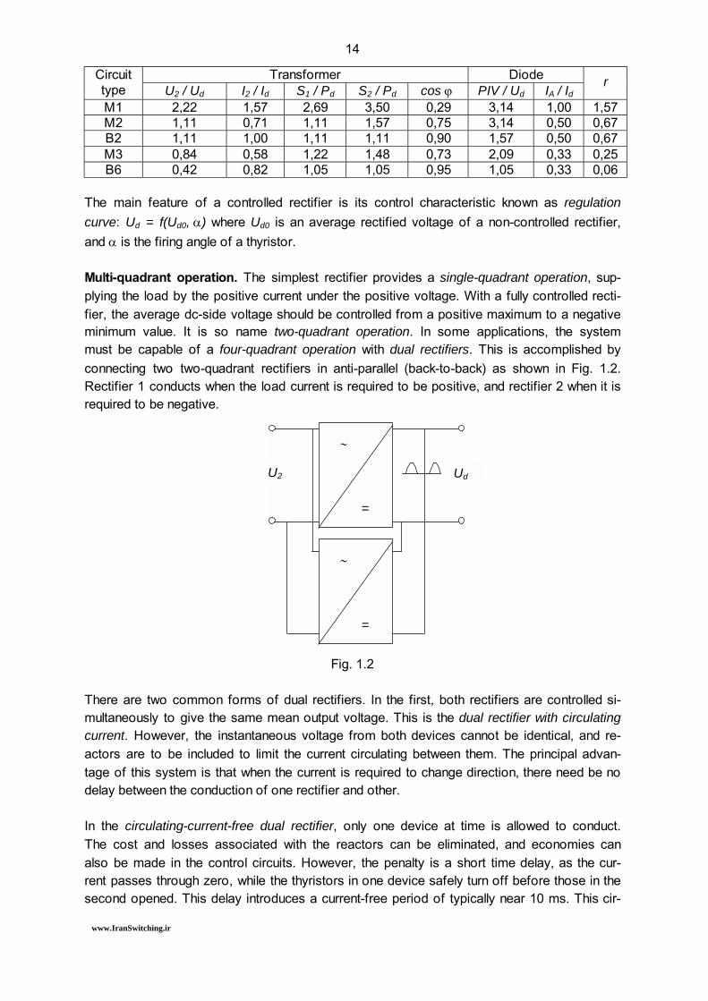
The main feature of a controlled rectifier is its control characteristic known as regulation curve: Ud = f(Ud0, α) where Ud0 is an average rectified voltage of a non-controlled rectifier, and α is the firing angle of a thyristor. Multi-quadrant operation. The simplest rectifier provides a single-quadrant operation, sup-plying the load by the positive current under the positive voltage. With a fully controlled recti-fier, the average dc-side voltage should be controlled from a positive maximum to a negative minimum value. It is so name two-quadrant operation. In some applications, the system must be capable of a four-quadrant operation with dual rectifiers. This is accomplished by connecting two two-quadrant rectifiers in anti-parallel (back-to-back) as shown in Fig. 1.2. Rectifier 1 conducts when the load current is required to be positive, and rectifier 2 when it is required to be negative.
Fig. 1.2 There are two common forms of dual rectifiers. In the first, both rectifiers are controlled si-multaneously to give the same mean output voltage. This is the dual rectifier with circulating current. However, the instantaneous voltage from both devices cannot be identical, and re-actors are to be included to limit the current circulating between them. The principal advan-tage of this system is that when the current is required to change direction, there need be no delay between the conduction of one rectifier and other. In the circulating-current-free dual rectifier, only one device at time is allowed to conduct. The cost and losses associated with the reactors can be eliminated, and economies can also be made in the control circuits. However, the penalty is a short time delay, as the cur-rent passes through zero, while the thyristors in one device safely turn off before those in the second opened. This delay introduces a current-free period of typically near 10 ms. This cir-
Ud
∼
=
∼
=
U2
www.IranSwitching.ir

15
cuit is by far the most common industrial four-quadrant dc system and is used in many de-manding applications where rapid control is required. Output characteristics. The practical output characteristics (load curves) of a controlled rectifier, shown in Fig. 1.3, a are the relation the rectified voltage Ud versus the rectified cur-rent Id. They demonstrate that the more the output current the less the output voltage. It is described by:
Ud = U0 – (ΣUAC + I2R2 + IdRs)
where U0 is the rectified voltage when Id = 0 (the infinite load of a rectifier), ΣUAC is the av-erage voltage drop of rectifier diodes or thyristors, I2R2 is the average voltage drop of the transformer, and IdRs is the average voltage drop per phase.
Fig. 1.3 A rectifier can maintain the continuous current operation or discontinuous current operation. The mode of operation depends on the load, the rectifier circuit, and the control method. On the continuous current operation, the output current is smoothed by load circuit inductance that is the output signal has no breaks. On the discontinuous current operation, the current waveform consists of separate pulses the length of witch depends on the inductance of the load circuit and a type of the rectifier. The ellipsoidal line on the output characteristics shows the discontinuous current boundary. The discontinuous current occurs to the left of this line and the continuous current occurs to the right. Consequently, the characteristics in the con-tinuous current region are linear, exhibiting only a slight droop. In contrast, in the discontinu-ous current region the curves are strongly nonlinear with the loss in output voltage. The dis-continuous current boundary equation seems as follows:
Idb = U0⋅sin α / (ωL) ⋅ (1 + π / m⋅ctg(π / m))
c.
discontinuous current bound
α = 0
Id α = max
Ud
a.
Id
Ud
Id
Ud
Id
Ud
b.
d.
www.IranSwitching.ir

16
where m is the number of pulses in the rectified voltage, L is the inductance of the rectified loop, ω = 2πf is an angular frequency, and f is the rectified ripple frequency. In accordance with the mode of operation, different rectifier circuits provide various output characteristics. They may be single-quadrant, two-quadrant, or four-quadrant as shown in Fig. 1.3, b, c, d. In the first case, the load voltages and currents are unipolar. In the second one, the load voltage may change the sign under the constant current direction. In the third system, both the load voltage and the load current are bi-directional. Summary. There are no power electronic systems without power or low-signal rectifiers in their structure. A great number of rectifier circuits work in different electronic devices. Re-markable, that harmonics generated by rectifiers fall into the frequency spectrum up to about 3 kHz and are conducted back into the power system. They produce a continuous distortion of the normal sinusoidal current waveform. The distortion frequencies are multiplies of the fundamental frequency 50 Hz as shown in Fig. 1.4.
Fig. 1.4
When the pulse number of rectifiers (m) grows, the frequencies of high order harmonics in-crease simultaneously and their relative magnitude decreases. Therefore, the trace of the input current becomes more sinusoidal, and output current is smoothed better. On the con-trary, when the firing angle of rectifier grows, harmonic frequencies and their magnitude do not change, but the phase shift of harmonics increases relatively supply voltage. This effect causes the consumption of reactive power from the supply lines with the power factor de-creasing.
1.2. Single-Phase Half-Wave Rectifiers
Diode rectifier with active load. A single-phase half-wave rectifier circuit (M1 recti-
fier) is presented in Fig. 1.5, a. The input and resulting output voltage waveforms of the half-wave rectifier circuit are shown in Fig. 1.5, b. If assume that during the positive alternation of the ac sinusoidal wave the anode of the diode D is positive and the cathode is negative, the diode will conduct since it is forward biased. The positive alternation of the ac will then ap-pear across the load Z. During the negative alternation of the ac cycle, the anode is made negative and the cathode is positive. The diode is reversed biased by this voltage and no significant current will flow through the load. Therefore, no voltage will appear across the load.
I Iout
ωt
www.IranSwitching.ir

17
Such type of the output waveform is called a half-wave signal because the negative half cy-cles have been clipped off or removed. Since the load voltage has only a positive half cycle, the load current is unidirectional and discontinuous, meaning that it flows in only one direc-tion and has breaks.
Fig. 1.5
The average value of one pulse of the dc output that a voltmeter reads is:
Ud = √2Us / π
i.e. 0,318 of the peak value of ac voltage Umax. The PIV of a diode should be π times larger than the average dc voltage developed. In this circuit,
Ur = Us / √2,
so the ripple factor of the output waveform is r = Ur / (2Ud ) = 1,57. Diode rectifiers with inductive load. In case of resistive-inductive load, Ud goes negative, and ac line current (the same as Id) is out of phase with the voltage (Fig. 1.6, a). The addi-tion of a freewheeling diode D1 shown in Fig. 1.6, b permits the load current curve to be con-tinuous and prevents Ud from going negative (Fig. 1.6, c). When D is off, D1 allows the load inductors current flow. If the inductance is large enough, Id never decays to zero. This oper-ating condition is known as continuous conduction. Diodes perform identical functions in other circuits where they are called bypass diode, flyback diode, or catch diode.
2π
PIV
Umax Urms
ωt
T
Ud
Ud
ωt
Us
b.
Z Us
D
Ud
Id ωt
UAC
a.
www.IranSwitching.ir

18
Thyristor rectifier. A single-phase half-period rectifier built on a thyristor is displayed in Fig. 1.7, a. Here, the value of the rectified voltage on the load depends on the firing angle α (Fig. 1.7, b):
Ud = Umax / (2π)⋅(1 + cos α).
Fig. 1.6 Fig. 1.7 The control curve, corresponding this equation, is given in Fig. 1.7, c. The firing angle is measured from the point of the sine waveform when the positive anode voltage appears on the thyristor. With a resistive load, the currents waveform matches the voltage shape. With the resistive-inductive load, the thyristor remains open on the negative anode voltage until the current through the thyristor decreases to zero. Thus, the output voltage can contain pulses from negative half waves of the voltage. Summary. The main advantage of the single-phase half-period rectifier is its simplicity. Nevertheless, it is rarely used in practice because of:
• this circuit has the low use of the transformer due to the poor secondary current shape;
• the use of a diode is also bad that is PIV significantly excels Ud; • the quality of the rectified voltage is low because of very high ripples and very
low power factor.
ωt
Ud
a.
Id ωt
Id
Z Us
D
D1
ωt
b.
c.
a.
c.
0,5 ωt
π / 2 π
Ud
Z
IG
α
ωt
ωt
Us
D
Ud
α
1 Ud / Ud0
b.
www.IranSwitching.ir

19
1.3. Single-Phase Full-Wave Rectifiers
Center-tapped transformer. A two-diode single-phase full-wave rectifier (midpoint
rectifier or M2 rectifier) is a parallel connection of two half-wave rectifiers. This system, shown in Fig. 1.8, produces a rectified rippled output voltage for each alternation of the ac input. The output of this device has twice the direct voltage value of the half-wave rectifier. The rectifier utilizes a center-tapped transformer that transfers alternating source voltage to the diode rectifier circuit. The anodes of each diode D1 and D2 are connected to opposite ends of the transformers secondary winding. The diode cathodes are then connected to-gether to form a common positive output. The load of the power supply should connect be-tween the common cathode point and the center-tap connector of the transformer. The transformer, two diodes, and the load form a complete path for current.
Fig. 1.8 When alternating voltage is applied to the primary winding of the transformer, it steps the voltage down in the secondary winding. The center tap serves as an electrical neutral or center of the secondary winding. Half of the secondary voltage will appear between center and upper taps of the secondary winding, and the other half between center and lower taps. These two voltage values are equal and will always be π radians (180 degrees) out of phase with respect to center point. Each diode must have the PIV rating of twice the value of the peak voltage developed at the output, since twice the peak voltage is present across the re-verse biased diode. Diode rectifier. Fig. 1.9, a shows the load voltage Ud, load current Id, and a diode inverse voltage UAC. The waveform of Ud is called a full-wave signal. The rectified voltage and cur-rent have the similar waveforms with two pulses during the period T. The main features of this circuit are:
Ud = 2√2U2 / π, Id = √2I2.
In any practical circuit an inductance presents and the current cannot break instantly. On the resistive-inductive load, the commutation interval γ (overlap) appears. It is shown on the cur-rent trace of Fig. 1.9, b. The reason is that the length of a diode conductive time is greater than the length of the positive voltage across the load.
D1
U2
D2 U2
U1
Vd
Z
www.IranSwitching.ir

20
Fig. 1.9 The commutation interval is an interval of simultaneous operation of two diodes. Current transitions from one device to another are called commutation processes. Because the di-odes in two phases are simultaneously open, in principle, it is the short circuit of the two phases and the output is the arithmetic mean of both phase voltages. The time period of the commutation process depends on the circuit inductance and the value of current. It is clear from the timing diagram that the commutation leads to the reduction of the average value of rectifiers output voltage. The commutation area is shading on the voltage trace. This addi-tional voltage drop raises the slope of the load curve shown in Fig. 1.3 that leads to deterio-rating the rectifier voltage stability. Thyristor rectifier. The average value of the thyristor rectified output voltage on the resis-tive load depends on the firing angle α and is expressed by the equation:
Ud = Ud0 / 2 cos α
where an average rectified voltage
Ud0 = 2Umax / π = 2√2U2 / π = 0,9U2
that is some less than rms secondary winding voltage of the transformer. The diagrams of gate pulses, voltages, and currents of the thyristor circuit with the resistive load are seen in Fig. 1.10.
Fig. 1.10
ωt
UAC
Ud
ωt
a.
Id ωt
b.
ωt
UAC
Ud
ωt Id
ωt γ
ωt
ωt
Ud
IG
α
UAC
Id ωt
www.IranSwitching.ir

21
When the resistive-inductive load is used, the continuous or discontinuous current may flow through the load. On the continuous current operation, the output current is smoothed by load circuit inductance that is the output has no breaks (Fig. 1.11, a). On the discontinuous current operation, the voltage and current waveforms consist of separate pulses the length of witch depends on the inductance of the load circuit (Fig. 1.11, b). Summary. The main advantage of the single-phase full-wave rectifier is its better use of the transformer and diodes than in half-wave rectifier. Nevertheless, the quality of the rectified voltage is low because of very high ripples and very low power factor. The main disadvan-tage of the two-diode full-wave rectifier is the requirement of center-taped transformer. Commutation improves the current waveform in the windings of the transformer and reduces the required transformer power. Obviously, commutation improves the power factor also.
Fig. 1.11
1.4. Single-Phase Bridge Rectifiers
Structure. To overcome the requirement of center-taped transformer, four diodes
can be used to form a full-wave single-phase bridge rectifier (B2 rectifier) shown in Fig. 1.12, a, b. By using four diodes or thyristors instead of two, this design eliminates the need for a grounded center tap.
Diode rectifier. During the performance of a bridge rectifier, two diodes are forward biased in each alternation of the ac input. When the positive alternation occurs, diodes D2 and D3 are forward biased, while D1 and D4 are reverse biased. This biasing conduction is due to the instantaneous voltage that occurs during the positive alternation. The conduction path is from the ac source, through diode D3, the load, then through diode D2, and back to the source. This causes the same alternation to appear across the load.
ωt
ωt
Ud
IG
α
a.
UAC
Id ωt
γ
Ud
IG
α
ωt
ωt
UAC
Id ωt
γ
b.
www.IranSwitching.ir

22
Fig. 1.12 During the negative alternation, current flows from the source through D4, the load, then through D1, and back to the supply line. This causes the second alternation to appear across the load in the same direction as the first alternation. This means that voltage developed across the load is the same for each alternation. As a result, both alternations of the input appear as output across the load changed to single directional current flow on dc output:
Ud = 2√2Us / π,
S = S1 = S2 = πPd / (2√2).
The timing diagrams of the circuit are the same as the full-wave rectifier, but the diode in-verse voltage is twice less since PIV across the diode is one-half that of the previous rectify-ing method. The secondary current of transformer is √2 times higher. The average current through the diodes equals to half of the dc load current: IA = 0,5Id. For high values of direct output voltage, the use of bridge rectifier is desirable. Thyristor rectifier. In thyristor rectifier,
Ud = Ud0 cos α = 2Umax / π cos α.
The input apparent power of thyristor rectifier:
S2 = 2Umax Id / π⋅ cos α.
The voltage as a function of firing angle is plotted by the control curve in Fig. 1.13. For 0 < α < π/2, the power flows from the ac to the dc side. For π/2 < α < π, the power flow is re-versed and the average value of the output voltage is negative. Therefore, over this range of α, power is flowing from the dc side to the ac side. It is called inversion. The circuit can op-erate only if the load current is positive. Otherwise, the thyristors could not conduct. When the region of the first and forth quadrants of the circuit characteristic is discussed, the circuit is a two-quadrant rectifier. Because the full ac voltage is applied to the conducting diodes in series with the load, the load voltage has a peak value twice that of the full-wave rectifier discussed earlier.
Fig.1.13
D1
D2
D1
D2
D3
D4
Us
b.
Us
D3
D4
Ud Ud
Z
a.
D1
D2
D3
D4
Us
c.
Ud
-1
1
inversion
rectification
0 π / 2 π
α
Ud / Ud0
www.IranSwitching.ir

23
Summary. In this rectifier, the use of transformer is better than in half-wave and full-wave rectifiers: the secondary current shape is more sinusoidal. Another advantage is higher ratio PIV / Ud that is better use of diodes. The additional pair of devices that leads to extra volt-age drop across the diodes is the disadvantage of the bridge rectifier. For this reason, some-times a single-quadrant semi-controlled bridge is used with two diodes and two thyristors (Fig. 1.12, c).
1.5. Three-Phase Full-Wave Rectifiers
Circuit diagram. Three-phase three-diode rectifier circuits (M3 rectifiers) produce a purer direct voltage output than single-phase rectifier circuits do, thus wasting less power. In Fig. 1.14, a, phases U, V, and W of the three-phase source are connected to the anodes of di-odes D1, D2, and D3. The load is connected between the cathodes of the diodes and the neutral of the wye-connected source. When phase U is at its peak positive value, maximum conduction occurs through diode D1, since it is forward biased. No conduction occurs through D1 during the negative alternation of phase U. The other diodes operate in similar manner, conducting during the positive ac input alternation and not conducting during the associated negative ac alternation.
Fig.1.14 In a sense, this circuit combines three single-phase half-wave rectifiers to produce a half-wave dc output. The phases of the three-phase system are shifted by 2π/3 radians (120 de-grees) to each other. Therefore, the voltage appearing across the diodes are 120 degrees out of phase. There is a period of time during each ac cycle when the positive alternations overlap one another, as shown in Fig. 1.15, a. During overlap time first period, the phase U voltage is more positive than the phase W voltage, whereas during the second interval, phase W is more positive. Diode D1 will conduct until first time period ends, then D2 will conduct beginning at the end of first period until the next area of overlapping is reached. A thyristor three-phase three-diode rectifying diagram on the resistive load is shown in Fig. 1.15, b. On the resistive-inductive load, the current continues through the diode or thyristor after the voltage has changed its sign. For that reason, the thyristor does not close at the zero-voltage instant, but remains open as follow from the Fig. 1.15, c.
Ud
Z
D1
a.
D2
D3
U
V
W Ud
D1
D
D3
U
U2
b.
U1
V
W Z
www.IranSwitching.ir

24
Performance. The voltage across the load rises to a peak value three times during each phase alternation of the input voltage. These peaks are 2π/3 radians apart. Since the direct output voltage never falls to zero, less ac ripple is presented, which results in a purer form of dc than single-phase rectifier produce. The rectified voltage of this circuit is:
Ud = (3Umax / π)⋅(√3 / 2)⋅ cos α = Ud0⋅ cos α.
Fig.1.15 In this equation, the phase voltage with amplitude value Umax is equal to:
Ud0 = 3√3√2Us / (2π) = 1,17Us.
The disadvantage of the three-phase three-diode rectifier is that the ac lines are not isolated. This lack of isolation, which is a direct connection to the ac lines, could be a hazardous safety factor. To overcome this disadvantage, a transformer can be used, as shown in Fig. 1.14, b. The secondary voltage can either be increased or decreased by the proper selection of the transformer. This will permit a variety of different values to be made available. The secondary voltage of the supply transformer is U2 = Us. When the load inductance is enough high, the output characteristics are linear. They are placed in two quadrants thus showing that the load voltage change its sign when α > π / 2 (Fig. 1.16).
Fig. 1.16
Id
α = π
α = π / 2
α = 0 Ud
c.
ωt
ωt
Ud
a.
Id
α
b.
Ud
ωt Id
ωt
ωt
ωt
α Ud
Id
γ
U W V U
www.IranSwitching.ir

25
Fig. 1.17 In Fig. 1.17 the three-phase six-diode rectifier is shown. The two parallel-connected three-diode circuits with additional reactor combine this rectifier. Two stars of the transformer sec-ondary windings are joined by such a way that the beginnings of windings are connected in the zero point of the first star and the ends of windings are connected in the zero point of another star. For this reason the circuit is known as a dual three-phase rectifier. The quality of the rectified voltage here is better due to the ripple amplitude is twice lower and the ripple frequency is twice higher. The circuit has high power factor cos ϕ = 0,955 and well uses the transformer. Reversible circuits. In the previous circuit, the polarity of the load voltage may be changed, but the direction of the load current remains constant. In Fig. 1.18, the back-to-back connec-tion of the two rectifiers has been produced to provide the reversible dual-controlled system. As a result, a new current loop was born, which do not includes the load. The current flowing through this loop built by the secondary windings and thyristors is known as a circulating cur-rent. The current value depends on the instant voltage differences both rectifiers and resis-tance of the loop. To avoid this current the firing angles of both rectifiers should be calcu-lated in accordance with the equations:
α1 + α2 = π; α1 α2 = π.
In this situation the circulating current will be discontinuous. In practice, there are three methods of thyristors control.
Z
L
D1
D
D3
D4
D5
D6
U
U2 U1
V
W
www.IranSwitching.ir

26
In the joint coordinated control systems, the firing unit performs the control by the next law:
α1 + α2 = π.
Thus, the mean values of the voltages are equal, but their instantaneous values are different and this difference is consumed by the circulating reactor L. The continuous current flows through the load, and the circulating current travels through the reactor, thyristors, and wind-ings.
Fig. 1.18
The output characteristics are linear (Fig. 1.19, a). The circulating current is a parasitic one, which results in the systems power increasing. The advantage of this system is that when the current changes its direction, there is no delay between the conduction of one rectifier and other.
Fig. 1.19
L
D1
D
D3
D4
D5
D6
U
U2 U1
V
W Z
Ud
Id
a.
Ud
b.
Id
Ud
c.
Id
www.IranSwitching.ir

27
In the joint non-coordinated control systems, the firing unit performs more simple control law:
α1 + α2 > π.
In this case, the mean values of the voltages are almost equal, and the difference of their instantaneous values is consumed by the circulating reactor L. The discontinuous current flows through the load, and the circulating current travels through the reactor, thyristors, and windings. The output characteristics are non-linear, with narrow discontinuous area (Fig. 1.19, b). Again, the parasitic circulating current results in the systems power rising. In the separate control systems, only one rectifier at time is allowed to conduct. In this case, each rectifier operates independently, and there is neither parasitic circulating current, no circulating reactor. Here, the firing unit switches off the first rectifier and with some delay switches on another rectifier. In order to prevent short-circuiting in rectifier leg, there should be a lockout time between a turn off of one rectifier and the turn on of the next. The delay must be larger than the maximum particle storage time of a rectifier. The effect of the dead time is a distortion on the voltage level. The discontinuous current flows through the load and the load curves become non-linear, with narrow discontinuous area (Fig. 1.19, c). In high quality systems, dead time compensation is mandatory to avoid voltage distortion caused the instabilities at low frequency. Hardware and software compensation is used.
Summary. Low degree of the transformer use and low power factor are the main disadvan-tages of this kind of rectifier. Enough high quality of rectified voltage with small ripples is its main advantage. The reversible rectifier provides the four-quadrant load operation with al-most constant voltage and constant current, though the additional losses may occur due to the circulating current. The circulating-current-free dual systems are used in many demand-ing applications where rapid control is required.
1.6. Three-Phase Bridge Rectifiers
SCR bridge. The full-wave counterpart of the three-phase full-wave rectifier circuit is
presented in Fig. 1.20. This three-phase bridge rectifier (B6 rectifier) requires six diodes for operation of the circuit. The rectifier can be considered as a series connection of two M3 rec-tifiers, where three devices are in a common cathode connection and three in a common anode connection. The anodes of diodes D4, D5, and D6 are connected together at one point, while the cathodes of diodes D1, D2, D3 are connected together at another point. The load should connect across these two points. This circuit does not require the neutral line of the three-phase source; therefore, a delta-connected source as well as a wye-connected source could be used.
Performance. The operation of the circuit is similar to single-phase bridge in many respects. Each diode in this device conducts during one-third of a cycle (120 degrees). Peak positive direct output voltage occurs during every π/60 radians of the three-phase ac input. Thus, the output voltage of the rectifier is twice greater than the output voltage of the mid-point M3 rec-tifier:
www.IranSwitching.ir

28
Fig. 1.20
Ud = (3√3Umax / π)⋅cos α = Ud0⋅cos α.
In this equation: Ud0 = 3√3√2Us / π = 2,34Us − phase voltage with amplitude value Umax. As α increases from 0 to π, the output voltage varies from Ud0 to −Ud0. The voltage ripple is less because the output voltage consists of six pulses per unit voltage period. The switching order of diodes of B6 rectifier in Fig. 1.21 is D1, D6, D2, D4, D3, D5. At least two diodes are simultaneously in the open state. On high load inductance, the forward current continues on the negative anode voltage and the closing of the device is delayed. Since the previously opened devices are not closed af-ter the opening the next devices, it is possible that three or even four devices are open dur-ing the commutation process. This means that there is more than one open diode in the cathode or anode group and the current is re-switched from one phase to another.
Fig. 1.21 The PIV of a diode is two times lower than in the mid-point rectifier since the diodes operate in the pair-wise series. The average and rms values of the diode current are:
Ud
U
V
W
U2
D1 D2 D3
U1
D4 D5 D6
UU, UW, UV
ωt
Ud
ωt
Id ωt
www.IranSwitching.ir

29
IA = Id / 3, Irms = I2 = Id / √3.
The rated power of the transformer is:
S1 = 1,05⋅UAC⋅Id.
The power factor:
cos ϕ = UAC⋅Id / S1 = 0,95.
Advanced bridge rectifiers. The circuit diagram of the rectifier built on GTO thyristors is shown in Fig. 1.22. Here, the device for recuperation of the accumulated energy of the load is added to the base circuit. It is the star- or delta-connected capacitor assembly in the recti-fier input. Every next thyristor is switched on by control pulse that is passed ahead the natu-ral firing instant. Simultaneously, the pulse is passed to close the thyristor, which conducts the current. As a result, the current of conducted device falls down, and the current of the switching on device rises quickly to the load value. Now, the input current of rectifier passes ahead the supply voltage, thus rectifier becomes the reactive power generator instead of consumer.
Fig. 1.22
In Fig. 1.23, the anti-parallel connection of the two rectifiers has been produced to provide the four-quadrant operation. The first rectifier conducts when the load current is required to be positive, and the second one when it is required to be negative.
Fig. 1.23
Vd
U
V
W
U2 D1 D2 D3
U1
D4 D5 D6
Ud
U
V
W
D1 D2 D3
D4 D5 D6
D7 D8 D9
D10 D11 D1
U
V
W
www.IranSwitching.ir

30
Synchronous bridge rectifier built on transistor switches is shown in Fig. 1.24. When volt-ages are low and currents are high, this circuit has advantage due to decreasing the losses. Moreover, thanks to the freewheeling diodes the four-quadrant operation is possible here because of the switches opening during the regeneration periods. Of course, the gate driver of the switches is more complicated than thyristors have.
Fig. 1.24 Summary. The three-phase bridge rectifiers are predominant because of their good techni-cal properties:
• low ripple; • high power factor; • simple construction; • low price.
Nowadays, they are used in powerful and small-power suppliers and in AC/AC converters with dc link. Nevertheless, the diode and thyristor three-phase bridge rectifiers have some disadvan-tages, which also are typical for all previous circuits:
• first, they do not allow regenerating energy back to the alternating current supply line without dual connection;
• second, their input current is distorted because of the diode commutation proc-esses.
Synchronous rectifiers based on transistor switches open the path to exclude these draw-backs.
Ud U V W T5 T4
T2 T1
T6
T3
www.IranSwitching.ir

31
Part 2. Inverters
2.1. Common Features of Inverters
Requirements. The process of converting dc to ac has been called inversion. An in-
verter converts the dc voltage to ac voltage of a definite frequency. Controlled semiconduc-tor devices, such as SCR, GTO thyristors, and transistors are used in inverters. The input dc voltage may come from the rectified output of an ac power supply, in which case it is called a dc link converter. Alternately, the input dc may be from an independent source such as a dc voltage source or battery. The ac output frequency of inverter is pre-cisely adjustable by control the switching frequency of the inverters devices. This is usually determined by the frequency of a clock oscillator in the switching control section of the in-verter. A requirement for a load control by the use of a variable frequency supply is that the applied voltage or current waveforms contain the minimum possible distortion. The best solution would be an inverter that generates sinusoidal waveforms, because the sine wave form is usually the most desirable for many applications. However, such a device would be elabo-rated on expensive since it would require a large number of switching elements. Therefore, the ac output of practical inverters will inevitably have a certain amount of harmonic content. There are two ways by which the harmonic content can be brought down to a low value or at least within acceptable limits:
• one method is to use a filter circuit on the output side of the inverter; of course, the filter will have to handle the large power output from the inverter;
• the second scheme employs a modulation strategy that will change the harmonic content in the output voltage in such a way that the filtering needed will be mini-mal or zero depending on the type of amplification.
Different classes of inverters are widespread. Single-phase and three-phase inverters. Inverters are usually designed to provide either single or three-phase output. Larger industrial applications require three-phase ac. Low-signal half wave inverters pass the electrical energy during one alternation. These inverters are used when the power of the load is 100 200W. Offline and online inverters. The second classification refers to offline inverting and online inverting. If the only source of the load ac line is the inverter, the inverter is called an offline inverter or autonomous inverter. Some popular offline inverters have the same topology as the controlled rectifiers discussed above. On the other hand, if the inverter is the part of the common power line supplies, the inverter is called an online inverter or a line-fed inverter.
www.IranSwitching.ir

32
Voltage source and current source inverters. In accordance with the circuit electromag-netic processes, voltage source inverters and current source inverters are distinguished. A voltage source inverter (VSI, or voltage stiff inverter) forms the voltage with required proper-ties: magnitude, frequency, and phase. This is the most commonly used type of inverter. The signal that it provides on the output side functions as a voltage source. The diagram of the inverters voltage and current is shown in Fig. 2.1, a. This inverter has the low internal im-pedance. Generally, it has a capacitor of high capacity connected across the supply source that keeps the voltage constant.
Fig. 2.1
Other feature is the bi-directional input current of VSI. To provide this peculiarity, the switches must be constructed on the full controlled devices (transistors, GTO thyristors or MCT) with freewheeling diodes. The output current of the VSI is shaped according to the voltage value and the load resistance. There is usually provision for adjustment the output voltage of the inverter. One of the two ways is commonly used. Varying the dc input voltage supplied the inverter may vary the out-put voltage. In this case, the adjustment is outside the inverter and is independent on the inverter operation. The alternative way of ac voltage variation is within the inverter by a modulation technique. A current source inverter (CSI) is the source of the current with the required properties: magnitude, frequency, and phase. The input circuit of the current source inverter has the properties of the dc current source. The switches of the inverter periodically change the out-put current direction. The load of the inverter has the properties of the voltage source with almost zero impedance. Thus, the output voltage of the CSI is shaped according to the volt-age drop on the load caused by the output current. The diagram of the inverters voltage and current is presented in Fig. 2.1 ,b. Commonly used inverters are neither perfect voltage source nor perfect current source in-verters. They approximate more or less the properties of both in dependence of an induc-tance and capacitance of the circuit.
Uout
ωt
a.
Iout
ωt
Iout
ωt
b.
Uout
ωt
www.IranSwitching.ir

33
Control methods. Another classification refers to a method of control. There are a block control (other names are square-wave control and six-step control) principle and a pulse control principle. According to the first principle, ones opening and closing a semiconductor switch forms the positive or negative half period of the ac signal. Thus, the rectangular volt-age blocks are formed at the output of the inverter. The advantages of the square-wave in-verter are high efficiency (near 98%), potentially good reliability, and high-speed capability. In such circuit, harmonic voltage amplitude is inversely proportional to the harmonic order and hence there are no pronounced high-order harmonics. These are filtered out by the load inductances. High-frequency operations are possible by increasing the output frequency. Faster switching devices such as MOS transistors and IGBT can be used to achieve this performance. However, it suffers from low-voltage pulsations and possible instability. The sinusoidal out-put voltage cannot be achieved using the block control principle. The output voltage diagram of the block control inverter is a piecewise curve, which significantly differs from the sinusoi-dal curve. The block control inverters are usually used in low-power industrial applications where the voltage range is limited to ten to one and dynamic performance is not important. Neverthe-less, they are enough prospective systems thanks to the new vector methods development. If the pulse control is used, the controlled ac signal is formed by one of the pulse modulation method. A large number of modulation techniques exists each having different performance notably in respect to the stability and audible noise of the driven load. PWM technique. The pulse width modulation, or PWM method is now gradually taking over the inverter market in control applications. This technique is characterized by the generation the constant amplitude pulses in which the pulse duration is modulated to obtain necessary specific waveform. The principle of PWM is illustrated in Fig. 2.2. The sinusoidal modulating signal Um referrers the required output waveform. The high-frequency triangle carrier signal Uc is synchronized by the ac supply voltage. Usually, the carrier frequency is much greater than the modulating frequency. The natural intersections of Um and Uc determine both the offset and duration of the modulated pulses. In PWM waveform of pulse pattern is dependent on the ratio of the peak Um to the peak Uc. The frequency ratio fc / fm is called the carrier ratio and amplitude ratio Um / Uc is called the modulation index. The carrier ratio determines the number of pulses in each half-cycle of the inverter output voltage and the modulation index determines the width of the pulses and hence the rms value of the inverter output voltage. The ideal maximum modulation index is equal to unity. Various PWM schemes allow Um / Uc < 1 that represents an important performance criterion as the inverter maximum power depends on the maximum voltage at load terminals.
www.IranSwitching.ir

34
Increase of the output voltage is possible by making Um / Uc > 1, but the output is then no longer proportional to modulation index. This condition of overmodulation leads to increasing the harmonic current and can also result in undesirable large jumps of voltage.
Fig. 2.2 Using the PWM technique, low-frequency current pulsations are virtually eliminated since negligible low-order harmonics are present. When the modulation is provided by a sinusoidal curve, the output of the converter is the pulsed voltage with an average sinusoidal value. Hence, this is an ideal solution where a power electronics system is to be used across a wide frequency range. Since voltage and frequency are both controlled with the PWM, quick response to changes in demand voltage and frequency can be achieved. PWM inverter efficiency typically ap-proaches 98% but this figure is heavily affected by the choice of switching frequency the higher the switching frequency the higher the losses. In practice, the maximum fundamental output frequency is usually restricted to 100 Hz in the case of GTO or 2 to 50 kHz for a tran-sistor-based system. The upper frequency limit may be improved by making a transition to a less sophisticated PWM waveform with a lower switching frequency and ultimately to square wave if the application demands. However, with the introduction of faster switching power semiconductors, these restrictions to switching frequency and minimum pulse width have been eased. Their suppression is a matter for the power electronic designer and suitable internal measures can keep such emission under control. Summary. Inverters are the significant building blocks of ac electronic systems. So far as the ac loads dominate in industry, business, and life, inverters become the objects of choice for many designers and customers. Inverters do not themselves radiate an essential level of harmful electromagnetic energy. The electromagnetic fields in the immediate vicinity (<100 mm) of the inverter can be enough high, but these diminish quite quickly according to the inverse square low and are
Uc U
Um
ωt
ωt
Iout
Uout
ωt
T
www.IranSwitching.ir

35
insignificant at a distance of about 300 mm. When inverters are mounted in metal enclo-sures, the electromagnetic radiation is largely eliminated. Nevertheless, high frequencies superimposed on a sinusoidal waveform of supply draw a non-sinusoidal current and distort the ac voltage as shown in Fig. 2.3. They cause additional losses in different items of plant. Harmonic distortion can be looked upon as a type of elec-trical pollution in a power system and is of concern because it can affect other connected equipment. For example, a total harmonic voltage distortion of 2,5% can cause an additional temperature rise of 4°C in induction motors. In cases where resonance can occur between the system capacitance and reactance at harmonic frequencies, voltage distortion can be even higher.
Fig. 2.3
2.2. Voltage Source Inverters
Inverting mode of thyristor rectifiers. The early-discussed full-wave controlled rec-
tifier circuits can operate as online inverters when the firing angle α > π/2. The voltage and current diagrams of a midpoint three-phase converter, shown in Fig. 1.14, are presented in Fig. 2.4. Here, the negative ac voltage is directed against the current, therefore the negative active power is moved to the supply line.
Fig. 2.4
I Iout
ωt
β α
ωt
ωt
Uout
UAC
Iout
ωt
γ
www.IranSwitching.ir

36
In the inverting mode, it is often more convenient to express the firing angle in terms of the angle of advance from the end limit of the interval available for successful commutation than as a delay α from the beginning of the interval. This angle is usually denotes as β. Then,
α + β = π
and
cos α = −cos β.
To complete the commutation before the limit available when there is overlap, the angle β should be greater than the commutation interval γ. The commutation interval is variable and dependent on the dc load current. To take care of this and the turn-off time of the thyristor also, it is usual to provide a minimum angle of safety that is called the extinction angle: β γ. For stable inverter operation when the possibility of commutation failure exists, it is desirable to employ a closed-loop gate control, which will automatically ensure a safe minimum extinc-tion angle. Single-phase block-controlled VSI. Fig. 2.5, a shows the half-bridge configuration of the single-phase VSI. Switches T1 and T2 may be BJT, MOSFET, IGBT, GTO thyristors, or SCR with commutation circuit. Freewheeling diodes D1 and D2 are known as feedback diodes be-cause they can feed back load reactive energy.
Fig. 2.5 Waveforms are shown in Fig. 2.5, b. During the positive half-cycle of the output voltage, the switch T1 is turned on, which makes Uout = +Ud / 2. During the negative half-cycle the switch T2 is turned on, which makes Uout = –Ud / 2. Note that prior to turning on a switch, the other one must be turned off; otherwise both switches will conduct and short circuit the dc supply. If the load is reactive, the output current lags the output voltage, as shown in Fig. 2.5, b. Note that Uout is positive during 0 < t < T / 2; that is, either T1 or D1 is conducting during this interval. However, Iout is negative at the beginning of the phase; therefore D1 must be con-ducting during this part of interval. Later, the load current is positive till T / 2 and therefore T1
–
+
D2
D1
Uout
T2
T1
a.
Ud / 2
Ud / 2
Uout
Iout
ωt
U,I
ωt
b.
ωt
T2on
T1on
www.IranSwitching.ir

37
must be conducting during this part of interval. The feedback diodes conduct when the volt-age and current are of opposite polarities. Fig. 2.6 illustrates the single-phase full-bridge VSI. It consists of two legs. Each leg includes a pair of transistors with anti-parallel freewheeling diodes discharge circuits of reverse cur-rent. In case of resistive-inductive load, the reverse load current flows over these freewheel-ing diodes. The diodes provide an alternate path for the inductive current, which continues to flow when a switch is turned off. When regeneration occurs, the roles of the switch and di-ode reverse. The diode now returns the regenerated power to the dc supply while the switch carries the reactive voltage.
Fig. 2.6 With the block control, the two transistors in each leg may be switched in such a way that when one of them is in its off state, the other is on (Fig. 2.7,a). Therefore, the two switches are nether on simultaneously. In practice, they are both off for a short time interval, known as a blanking time, to avoid short-circuiting of the dc input. In analyzing the circuit the blank-ing time is neglected since it is assuming the switches to be ideal, capable of turning off in-stantaneously. Under enough load inductance, the output current will flow continuously. Therefore, the output voltage is solely dictated by the status of switches. The output voltage is reversible in polarity. In other cases, the bridge legs are switched such that their output voltages are shifted to each other. If the shift angle is equal to zero, the output voltage of the inverter is equal to zero. If the shift is π, the output voltage is maximal. The voltage waveforms of such block control are presented in Fig. 2.7,b. The shape of the output voltage differs significantly from the sinusoidal, besides the main harmonic. Therefore, the block control is well applicable in the control range where the frequency of the output voltage corresponds the main harmonic.
Single-phase PWM-controlled VSI. With the PWM control, the switching signals are gen-erated by comprising a switching-frequency carrier triangular waveform Uc with the modulat-ing signal Um as shown in Fig. 2.8. When Um > Uc, two transistors are turned on and two other are turned off. The switch duty cycle can be obtained from the waveforms:
q = ton / T = (1 + Um / Uc) / 2
+
–
Uout Ud
T4 T3
T2 T1
www.IranSwitching.ir

38
for turning on and
qoff = toff / T = 1 − q
for turning off. The duty cycle q can vary between 0 and 1 depending on the magnitude and the polarity of Um. The last equation shows that the average output voltage varies linearly with the modulating signal, similar to a linear amplifier. Due to the voltage jumps between +Uout and − Uout, this switching strategy is referred to as the bipolar voltage-switching PWM. The average output current can be either positive or negative.
Fig. 2.7
Fig. 2.8
toff U
ton
ωt
ωt
Iout
Uout
ωt
T
T4 D1, D4
D2, D3
Iout
U
U
ωt
T1, T4
ωt
a.
U
U
ωt
ωt
T1
ωt
Uout, Iout
b.
Uout
ωt
T2, T3 T2
T3
www.IranSwitching.ir

39
Many modern inverters have a selectable output switching frequency and the tendency is to use the highest output frequency to reduce audible noise (16 Hz to 50 kHz). The selection of the PWM switching frequency is a compromise between the losses in the load and the losses in the inverter. When the switching frequency is low, the losses in the load are higher because the current waveform becomes less sinusoidal. When the switching frequency in-creases, load losses are reduced but the losses in the inverter will increase because of the increased number of commutations. Three-phase block-controlled VSI. Three-phase inverters are commonly used to supply three-phase loads. The most frequently used three-phase bridge VSI is shown in Fig. 2.9. It consists of three legs, one per each phase. All inverter legs are similar; therefore the output of each leg depends only on dc supply voltage and the switch status. The output voltage is independent on the output load currents magnitude since one of the two switches in a leg is always on at any instant.
Fig. 2.9
With the block control, six different variants of open and close transistors may be presented. In any case, three transistors are opened together. When the load is delta-connected, each phase either gets the voltage of supply line or is shorted during π/3 radians. Therefore, the waveform of the phase voltage is rectangular as shown in Fig. 2.10. The sequence of switching is in the order T3T5T1, T5T1T6, T1T6T2, T6T2T4, T2T4T3, T4T3T5, and back T3T5T1. When the load is wye-connected, each phase is connected either in parallel to other phase or in series to other parallel-connected phases. Therefore, each phase gets the voltage equal to Ud / 3 or 2Ud / 3. The phase, line-to-line, phase-to-neutral, and line-to-neutral volt-ages then have the waveforms shown in Fig. 2.11. The firing of the three half-bridges are phase-shifted by π/3. When T1 is fired, point U is connected to the positive terminal of the dc supply, making UU = Ud / 2. When V4 is fired, point U is connected to the negative terminal of the dc supply, making UU = –Ud / 2. Waveforms of V and W are exactly the same at those of U, except that they are shifted by π/3. The line voltages are related to the point voltages as follows:
UUV = UU – UV, UVW = UV – UW, UWU = UW – UU,
+
–
W V
U
T5 T4
T2 T1
T6
T3
Ud
www.IranSwitching.ir

40
These voltages are quasi-square waves with π/3 pulse width. They have a characteristic six-stepped wave shape. For balanced three-phase operation, the voltage of the load neutral to supply neutral can be written as:
Fig. 2.10
Fig. 2.11
UUs 2Ud / 3
Ud / 3
Ud / 6
Ud
Ud / 2
ωt
UVs
UWs ωt
ωt
ωt
UN0 ωt
UWU ωt
UVW
ωt UUV
ωt
UW ωt
UV
ωt UU
1 2 3 4 5 6 1 2 3 4
T6 T3
T2 T5
T4
2π
T1
2π
2π ωt
ωt
ωt
www.IranSwitching.ir

41
UN0 = (UU + UV + UW) / 3.
From here, the load phase voltages may be obtained as follows:
UUs = UU – UN0, UVs = UV – UN0, UWs = UW – UN0.
They also have a six-stepped wave shape. The presence of six steps in the line-to-neutral voltage waveform is the reason for this type of inverter being called a six-step inverter. A Fourier analysis of these waveforms indicates a square wave type of geometric progression of the harmonics. That is, the line-to-line and line-to-neutral waveforms contain 1/5th of the fifth harmonic, 1/7th of the seventh harmonic and so forth. The line-to-line voltage contains an rms fundamental component of √6⋅Uline / π. Thus a standard 460 V load would require 590 V at the dc terminals. For this reason a 600 V dc bus is quite standard in US and other countries for inverter loads. Standard 380 V load require 487 V dc. Three-phase PWM-controlled VSI. Similar to the single-phase inverter, the objective in PWM three-phase VSI is to shape and control the three-phase output voltages in magnitude and frequency with an essentially constant input voltage. A power circuit, resembling the transistor inverter in Fig. 2.9, is the voltage source thyristor inverter shown in Fig. 2.12. With SCR thyristors and inductive-resistive load, additional components are needed for the forced commutation. On the other hand, when employing GTO, any additional circuitry is omitted.
Fig. 2.12 Each phase of the inverter comprises two main thyristors with anti-parallel diodes, two auxil-iary thyristors, a commutated capacitor and an air-cored inductor. A commutating process takes place as follows. Assume that the main thyristor D1 initially carriers the load current and the commutation capacitor of its phase is positively charged. Then firing of the auxiliary thyristor D11 causes D1 to be locked so that the load current flows temporarily through D11 thus recharging the capacitor. At the same time the resonant circuit is formed consisting of D11, its capacitor, inductor, and diode. When about a half period of the oscillation is con-cluded and the charging current tends to reverse its sign, D11 and D1 are blocked, which leaves the capacitor with opposite voltage, ready for the next commutation transient when
+
–
V
W
U
D5 D4 D6
D2 D1 D3
D41
D11
D51
D21
D61
D31
Ud
www.IranSwitching.ir

42
D4 has to be extinguished. The load current is now flowing through the diode of D4. If the current pulse through the resonant circuit is of sufficient magnitude as compared to the load current, the commutation is almost independent on the load. Voltage or current controller determines the firing instants for the main and auxiliary thyristors. To obtain balanced three-phase output voltages in a three-phase PWM inverter, the same carrier triangle voltage waveform is compared with three sinusoidal modulated voltages that are 2π/3 radians out of phase, as shown in Fig. 2.13. Changing the pulse width of each half-cycle of the inverter varies the output phase voltages UU, UV, UW of the inverter. The corre-sponding line voltages
UUV = UU – UV, UVW = UV – UW, UWU = UW – UU
have sinusoidal fundamental components.
Fig. 2.13 The inductive load applications of a PWM result in currents that respond only to the funda-mental component. But in view of the limited switching frequency, which is usually below 1 kHz for thyristors, the resistive load currents can no longer be considered close to sinusoi-dal as was possible with transistor inverters operating at a higher switching frequency. Hence, PWM thyristor inverters are naturally suited to act as voltage sources, presenting to the load pulse-width modulated rectangular voltages. This produces distorted line currents with low orders of harmonics and draws reactive currents of line frequency.
UUV
UW
UV
toff U
ton
ωt
ωt
UU T
ωt
ωt
ωt
www.IranSwitching.ir

43
Summary. This most commonly used inverting approach provides on the output side func-tions as a voltage source. The simplest method of VSI implementation deals with the use of thyristor rectifiers with the firing angles more than π/2. More effective and expensive are the transistor bridges with freewheeling diodes and block control. The best results gives multi-phase transistor PWM-controlled VSI.
2.3. Current Source Inverters
Features. CSI requires a dc current source at the input, as opposed to the dc voltage
source required in a VSI. Commonly, it has the large inductor connected in series to the supply source, which keeps the current constant, and the capacitor across the output. CSI can be used for such electrical equipment that needs the control of the current value: electric arc furnace, induction heating, etc. As compared to the VSI, they are not so widely used because the requirement of the resistive-capacitive load. Instead, the voltage inverter is used as a current source with appropriate current feedback. When using thyristors, CSI sometimes have advantages over VSI because of more simple switching circuits. Whereas each VSI can be used with most forms of ac loads, a specific design of CSI is usually adopted for different loads. Single-phase CSI. A forced-commutated CSI is the most widely used system at power lev-els in the range 50 3500 kW at voltages up to normally 700 V. High-voltage versions 3,3/6,6 kV have been developed, however they have not proved to be economically attrac-tive. The single-phase CSI is shown in Fig. 2.14. The single-phase bridge plays the role of the commutator here. For the current source mode, an inductor is included in the input circuit of the inverter. A capacitor is placed in the output as an energetic buffer between the pulsing inverter and the load. In addition, the capacitor is the instrument of the forced commutation of thyristors. When the thyristors D2 and D3 conduct the current, the input voltage charges the capacitor. In the instant of the thyristors D1 and D4 switching on, the previous thyristors will get the reverse voltage of the charged capacitor, which helps them close immediately. The capacitor begins recharging to other polarity, finishing it before the next switching in-stant. More the current, faster the capacitors recharging and shorter the time of the forced commutation.
Fig. 2.14
+
–
D1
D2
D3
D4
Uout Ud
www.IranSwitching.ir

44
Three-phase CSI. Fig. 2.15 shows a three-phase CSI. The dc current Id taken from a cur-rent source is sequentially switched at the required frequency into the load. The circuit commutation transient may be described as follows. With no commutation in progress, two thyristors, for example D1 and D6 curry the dc and the capacitor C1 is positively charges as a result of the preceding commutation. If the thyristor D2 is now turned on, D1 is extinguished in a rapid transient and D2 assumes the direct current. This is the starting condition of the commutation transient. While the current in U phase is now reduced towards zero, the cur-rent in V phase is rising. During this interval, U phase is fed through the capacitor C1 as well as the series connected capacitors C2, and C3. Eventually, diode D7 is blocked and the commutation is completed while D6 and D2 conducting. The diodes are required for decoup-ling in order to prevent the capacitors from losing their charge necessary for the next com-mutation.
Fig. 2.15 The idealized waveforms of the output currents are shown in Fig. 2.16. Each thyristor con-ducts for a π/3 radian. When a thyristor is fired, it immediately commutates the conducting thyristor of the same group (upper group D1, D2, D3, lower group D4, D5, D6). The diodes cause the charge to be held on the commutating capacitors. Without these diodes a capaci-tor would discharge through two phases of a load. The load voltage waveform is approximately sinusoidal apart from the superposition of volt-age spikes caused by the rise and fail of the load current at each commutation. The operat-ing frequency range is typically 5 to 60 Hz, the upper limit being set by the relatively slow commutation process. This system is used for single-motor ac drives of funs, pumps, ex-truders, compressors, etc. where very good dynamic performance is not necessary and a supply power factor, which decreases with speed, is acceptable.
L
D11
V
W
U
C1
C3
D8
D12
D9
D10
D5 D4 D6
D7
D2 D1 D3 +
Ud
C2
www.IranSwitching.ir

45
Fig. 2.16
CSI built on GTO thyristors. The circuitry of the inverter is considerably simplified when GTO thyristors or transistors are employed where the load and the line currents may be width modulated and approach sinusoidal waveforms. These circuits do not need the diodes D7 D12 and capacitors are only between phases U, V, W. Such capacitor bank performs the following functions:
• during switchover of current between devices, the load current is provided by the capacitors, which assist the commutation process;
• capacitors filter current harmonics and make the load current essentially sinusoi-dal;
• voltage spikes are reduced significantly.
A major disadvantage of this scheme is the potential for resonance between the capacitors and the load inductances. Care must be taken to avoid impressing current harmonics into the load-capacitor network, which will excite one of the system resonant frequencies. This possibility can be avoided by careful use of PWM. However, since the load parameters must be known to implement such an approach, the system is presently not popular for general-purpose applications. Summary. The main features of forced-commutated CSI may be list as follows:
• they cannot operate with no loading and overloading; • their output voltage waveform depend on the load value; • they are enough slow devices because of reactive elements in their inputs and
outputs; • the size and cost of the ac commutating capacitors and the inductor are the sig-
nificant disadvantage of this inverter; they are to be large because they must ab-sorb the total energy stored in the load when the current is commutated.
IW
IV
IU
ωt
I
ωt
ωt
D2
D1 D1
D4
D5
D6
D3
www.IranSwitching.ir

46
2.4. Resonant Inverters
Objectives. In all topologies discussed above, the electronic devices operate in a
switch mode where they are required to turn on and turn off the entire load current during each switching. In these operations, the switches are subjected to high stresses and high power loss that increases linearly with the switching frequency. Another significant drawback of these operations is the electromagnetic noise produced due to large current and voltage transients. These shortcomings of switching converters are exacerbated if the switching fre-quency is increased in order to reduce the converter size and weight and hence to raise the power density.
Therefore, to realize high frequencies, the switching processes should be produced when the voltage across the switch and/or current through it is zero at the switching instant. Reso-nant inverters are the switching converters, where controllable switches turn on and off at zero voltage (zero-voltage switch, ZVS) and/or zero current (zero-current switch, ZCS). The resonant inverters are defined as the combination of inverter topologies and switching strategies that result in zero-voltage and/or zero-current switching:
• resonant dc-link inverters; • load-resonant inverters; • resonant-switch inverters.
Supply-resonant inverters. The input voltage of the ZVC circuit, presented in Fig. 2.17 and known as soft inverter, is a pulsating dc that oscillates around its average level. As a result, the input voltage remains zero for a finite duration, during which the status of the inverter switches changes. The circuit is controlled as follows.
Fig. 2.17 In initial state, the capacitor is discharged. All inverter switches are turned on at zero volt-age, applying zero volts to the load and shorting out the capacitor. The inductor current ramps up through the switches. When the inductor current reaches an appropriate level, one
+
–
Uout
L
C Ud
T4 T3
T2 T1
www.IranSwitching.ir

47
switch in each leg opens and applies voltage to the load. The capacitor voltage then rings up to a value exceeding the supply while the inductor current decreases. The oscillation continues with capacitor voltage now decreasing. The supply across the in-verter leg has the form of a series of pulses with the same waveform as the capacitor volt-age. When the capacitor voltage decreases to zero, the anti-parallel diodes clamp the ca-pacitor voltage from going negative in effect placing a short across the capacitor and mo-mentary discharging it. Then, the process repeats. This circuit has no ability to give pulses with continuous variation in pulse width as with the conventional inverter. The output voltage must be controlled by block modulation rather than PWM. However, the resonance is at such a high frequency (50 − 100 kHz) that this does not limit the smoothness of the output current. Load-resonant inverters. These inverters include the output LC resonant circuit between the switching module and the load. The parallel and series resonant circuits and their com-binations as mixed resonant circuits are used in load-resonant inverters for this purpose. The power flow to the load is controlled by the resonant impedance, which in turn is con-trolled by the switching frequency. Resonant inverter displayed in Fig. 2.18 consists of a switching circuit T1 T4 and LC reso-nant circuit that form an alternating voltage for the load. The maximum frequency of the tank circuit is near the communication frequency of the switches. The frequency of the resonant inverters cannot be changed by the reference signal of the control system. Such inverters are used in electro-thermal processes for supply the heating equipment. They are suit for microwave furnaces and ultrasound equipment where sources are needed without control. The resonant inverter for dc voltage load has the rectified output.
Fig. 2.18 Resonant-switching inverters. Resonant-switching inverters have also been termed ZCS quasi-resonant inverters. The inverter has the same circuit as shown in Fig. 2.14. The input reactor and the output capacitor of the circuit make up an LC loop with a switching device between them. The resonant loop parameters and switching frequency are selected by such a way that the output current is discontinuous. When the current falls to zero, the thyristors
+
–
L C
Ud
T4 T3
T2 T1
Uout
www.IranSwitching.ir

48
switch off. Thanks to zero-current switching, the losses are very low and the switches may be low-power devices. Moreover, the discontinuous current waveform results in high-speed voltage amplitude regulation.
Summary. Significant decreasing of the thermal load and stress commutation processes lead to the growing of inverters reliability and frequency range. Nevertheless, most of de-signs of this type share common problems:
• first, the resonance inherently causes higher voltages than that of the supply, which place higher stresses on the power switches and the load; this can be overcome with addition of other switches and energy storage elements to absorb excess energy.
• second, they require more complex control systems because the instant of switching has to be varied with the load to maintain resonance.
www.IranSwitching.ir

49
Part 3. AC/AC Converters
3.1. AC Voltage Regulators
Classification. A converter that changes an ac supply to the ac supply with alternative volt-age, frequency, phase, or shape is called an AC/AC converter. The simplest one is voltage regulator, which changes ac voltage without frequency variation. Others are direct frequency converter that changes frequency and voltage shape and dc link frequency converter. In the last of them, a rectifier is used as a voltage-regulating front-end system and an inverter that generates an ac voltage with certain frequency. Single-phase voltage regulator. The ac source provides the means of natural commutation of the conducting switches. A pair of SCR connected in inverse-parallel or a triac can per-form the function of an electronic switch suitable for use with ac supply. The power circuit of a single-phase ac voltage regulator supplying a resistive-inductive load is shown in Fig. 3.1, a. If necessary gating pulses IG are applied to the SCR while its respec-tive anode voltages are positive, current conduction is initiated.
Fig. 3.1
D1
b.
ωt
U, I
Iout
γ
D2
Uout
Z
IG
α
ωt
c.
Uout Uin
U, I
Iout Uout
α=γ ≤ ϕ
ωt
a.
www.IranSwitching.ir

50
The conduction angle depends on the firing angle α, measured from anode zero voltage, and the phase angle ϕ of the load for sinusoidal supply. Thyristor D1 is fired at α and thyris-tor D2 is fired at π + α. When D1 turns on at α, the supply voltage is applied to the load. The load current builds up at α and decays to zero at some angle γ. When D2 turns on at π + α, a negative current pulse flows in the load. The waveforms of the load voltage Uout and load current Iout are shown in Fig. 3.1, b for the situation when α > ϕ. In this case, Iout is discon-tinuous. Fig. 3.1, c shows waveforms for the situation when α ≤ ϕ. In this case, Iout is con-tinuous and sinusoidal. When α < ϕ, the thyristor will be fired at ωt = α, but it will turn on at ωt = ϕ, The effective load voltage can be varied from zero, corresponding to extinction of both thy-ristors, to almost full supply voltage, corresponding to full conduction of both devices. When a switch is conducting, its forward voltage drop is of the order of one volt and this constitutes a reverse voltage on the reverse-connected thyristor, which is held in extinction. A current flowing in SCR D1, for example, serves to reverse-bias SCR D2. This cannot switch on, re-gardless of firing conditions until the current in D1 has fallen below its holding value (a few mA). Three-phase voltage regulator. For high-power loads, three-phase regulators are used. Fig. 3.2 shows three-phase voltage regulators comprising inverse parallel-connected thyris-tors in each supply line of a load. In the first circuit, the thyristor switches are in lines and the load is star-connected.
Fig. 3.2
In the other circuit the thyristor switches are connected in series with the phase loads to form a delta connection. Analysis of the star-connected three-phase regulator is complex because operation of one phase is dependent on the operation of the other phases. However, the operation of the delta-connected regulator can be studied on a per-phase basis because each phase is connected across a known supply voltage. Alternative connections are avail-able also, but the principles are similar. Often, the converters, shown in Fig. 3.2, are used to control the voltage applied to the load (motors, lights) and in this way soften the effects of switching the load direct-on-line.
Z
D2
D3
D6
D5
D4
V
U
a.
D1
Uin
W
Z
Z
D2
D3
D6
D5
D4
V
U
b.
D1
Uin
W
Z
Z
Z
www.IranSwitching.ir

51
Summary. Voltage regulators control the ac load voltage without frequency changing. They are low-effective devices and thus have no use in precision systems. The most usual appli-cations are the soft starters for induction motors where the voltage control provides smooth jolt-free acceleration. Also, such converters employ as combined soft starters, power-factor correctors, and energy-saving devices. In addition to the voltage control, a crude form of fre-quency control is possible by modulating (varying cyclically) the thyristor firing angles at the required output frequency.
3.2. Direct Frequency Converters
Frequency converters. Frequency converters (changers) transform an ac of one frequency to ac of other frequency. They are classified as the direct frequency converters and convert-ers with intermediate dc link. Direct frequency converters do not contain energy storage in the intermediate circuit. Their ac input frequency is directly converted to the ac output fre-quency. The most popular types of direct frequency converters are naturally commutated cycloconverters and matrix frequency converters. Cycloconverters. Cycloconverters are the naturally commutated frequency converters that are synchronized by supply line. Commonly, they are used in high power applications up to tens of megawatts for lowering frequencies of such low-speed machines as rolling mills, hoists, excavators, and screw propellers. A thyristor, closing on natural commutations, i.e. turns off on zero current, is the almost only device that can meet the switch voltage and cur-rent rating needed at this power levels. 3-, 6-, 12-, and 24-pulse cycloconverters are used. The main feature of these circuits is that only standard line-commutated thyristors are re-quired, which have been in use for many years up to the highest power ratings. Also, the cost of the thyristors is reasonable since no particular specifications with regard to turn-off time are necessary. Single-phase cycloconverter. Fig. 3.3 shows the single-phase cycloconverter. Its left and right converters are the positive and negative controlled rectifiers, respectively. If only left is operated, the output voltage is positive. If the right converter is operated, the output voltage is negative. Let the amplitude of the control signal Uc be such that the output voltage Uout is maximal. This means that the firing angles of the two converters are zero, that is, αleft = αright = 0. Dur-ing the positive half-cycle of Uc the left converter is fired, and during the negative half-cycle the right converter is fired. The output voltage waveform of Fig. 3.4, a describes the case when the fundamental output frequency is one-third the input frequency. Let the polarity of the control voltage Uc represents the polarity of the output voltage Uout. And the amplitude of Uc represents the desired average output voltage. The frequency of Uc represents the fundamental output frequency of Uout. The supply voltage Uin is shown in Fig. 3.4, a.
www.IranSwitching.ir

52
Fig. 3.3
Fig. 3.4
The waveform of the output voltage at a reduced value of the control voltage is shown in Fig. 3.4, b. If the control voltage varies with time during each half-cycle instead of remaining con-stant, the firing angles change during the half-cycle. This reduces the harmonic content in the output voltage as shows Fig. 3.4, c.
Uc (α1 = α2 =π / 6)
Uout
Uin
ωt
U ωt
ωt
Uc (α1 = α2 =0)
a
Uout
ωt
ωt
b. Uout ωt
c.
α1 α2
±Uc
Uin
D1 D2
D3 D4
D5 D6
D7 D8
Uout
www.IranSwitching.ir

53
Three-phase cycloconverters. The circuit diagram and the output voltage traces of a 6-pulse cycloconverter are presented in Fig. 3.5, a, b.
Fig. 3.5 The device has the 3-phase input and single-phase output and consists of two anti-parallel three-phase bridges. The thyristors of the first bridge conduct on the positive half-wave of the output and the thyristors of the second bridge conduct on the negative half-wave of the output. The firing angles are adjusted by such a way that the output voltage is kept close to sinusoidal form. There are several ways to control the cycloconverter. The simplest way is the triangle control, under which the firing angles of the active bridge can be changed linear. Output voltage alters nearly sinusoidal in this case. Thyristors are closed by the supply volt-age commutation. Thus, the frequency of the output voltage cannot precede the frequency of the supply voltage and is always at least twice lower. For smooth commutation of the cur-rent from one bridge to another, the firing angle is momentarily changed above π/4 radians and the bridge goes into the inverter operation mode. Although the output voltage of a cycloconverter can be either positive or negative, the output current can only be positive. To obtain bilateral load current, a negative converter is usually placed in parallel with the positive one. It can carry negative load current. Such combined circuit is known as a four-quadrant naturally commutated cycloconverter that produces an ac output voltage for the bi-directional output current. The large number of thyristors seems at first sight staggering. For the six-pulse converter with three-phase output shown in Fig. 3.6 a minimum of 36 thyristors is required. This indi-
a.
b.
Uin
D1 D2 D3
D4 D5 D6
D7 D8 D9
D10 D11 D12
Uout
ωt
www.IranSwitching.ir

54
cates that cycloconverters are mainly of interest for large systems, where parallel thyristor branches would be necessary in other converter circuits. An important restriction is the limi-tation of output frequency, which is caused by the discrete nature of the control process and
Fig. 3.6 the presence of a carrier frequency, since the output voltages are assembled from sections of the line voltages. As the output frequency rises, the output voltages are tracking the sinu-soidal references with increasing errors and consequent distortion. The frequency range
0 < f < m⋅f0 / 15 is usually considered as the useful range of operation, where f0 is the line frequency and m is the pulse number. With a 50 Hz net and a three phase bridge circuit (m = 6) this results in fmax = 20 Hz. Of course, if a three-phase line of higher frequency is available, the range of output frequency is extended accordingly; this may be the case of vehicles or ships, when a diesel- or turbine-driven generator provides on-board power. Other circuit of the direct frequency converter is given in Fig. 3.7. It is a cycloconverter with polyphase outputs. Again, this approach uses three three-pulse controlled converters to cre-ate the three output voltages. Each converter has six thyristors, three to carry positive load current and three to carry negative load current often with a transformer with three complete sets of three-phase secondary windings. It is of interest to note that the nature of the load
Uin Uout
www.IranSwitching.ir

55
supplied by the cycloconverter is unimportant. In particular, there is no difference whether the load is active or passive because operation in all four quadrants is possible.
Fig. 3.7 When considering the effects of a converter on the line-side currents, it is helpful to remem-ber that a symmetrical three-phase system of sinusoidal voltages and currents results in constant net power. Since the cycloconverter contains only switches but no storage devices (apart from the unavoidable leakage inductances, protective circuits, etc.), the total three-phase input power corresponds the output power. Nevertheless, there will be reactive power at the line side, which is inherent in the control of line-commutated converters by delayed firing. Matrix frequency converters. Theoretically, it is possible to replace the multiple conversion stages and the intermediate energy storage elements by a single power conversion stage called the matrix converter. Matrix converters may become attractive at low power rating as an alternative to cycloconverters.
Fig. 3.8
Such converter uses a matrix of semiconductor bi-directional switches connected between each input and output terminal as shown in Fig 3.8. With this general arrangement of switches, the power flow through the converter can reverse. Because of the absence of any energy storage element, the instantaneous power input must be equal to the power output, assuming idealized zero-loss switches.
Uin
Uout
www.IranSwitching.ir

56
As far as this converter provides output voltage directly from the multiphase network voltage, the peaces of the output voltage conduct to the outputs at appropriate moments. That is why the output voltage has the required frequency, number of phases, phase, amplitude, etc. Its parameters can be freely varied in wide range. In Fig. 3.9, the possible realization of the ma-trix frequency converter is given as a forced-commutation converter that provides the output voltages directly from the multiphase mains.
Fig. 3.9 In this cross bar arrangement, the three load terminals are alternately connected to the three supply terminals. The limit frequency is only constrained by capabilities of semiconductors. For the control of the matrix converter, the pulse-width modulation, pulse-amplitude modula-tion, and vector-modulation principles are used. However, the phase angle between the voltages and currents at the input can be controlled and does not have to be the same as at the output. In addition, the form and the frequency at the two sides are independent. The switches in a matrix converter must be bi-directional, that is, they must be able to block volt-ages of either polarity and be able to conduct current in either direction. This switching strat-egy permits the highest possible output voltage; at the same time the reactive line-side cur-rent is reduced since the current flows only in the center region of the line voltage periods. Such switches are not available and must be realized by a combination of the available
Uout Uin
www.IranSwitching.ir

57
switches. Capacitive filters can remove the high frequency components of the line currents. There are also limits on the ratio of the magnitudes of the input and output quantities.
Summary. The main advantage of the direct frequency converters is that they do not con-tain energy storage in the intermediate circuit. Thanks to the direct conversion input to the ac output frequency, they are very effective. The common used direct frequency converters are naturally commutated cycloconverters, but their disadvantages deal with very low frequency output, which cannot be higher than 0,4 of supply frequency. The power factor of cyclocon-verters is low also. That is why the most prospective are matrix frequency converters.
3.3. DC Link Converters
PWM converters. A PWM converter represents the frequency converter with dc link.
It consists of a non-controlled or controlled rectifier, and an inverter with pulse-width modula-tion. The maximum power of such converter may approach megawatts. Commonly, a con-verter is connected to the supply line through the chokes that defend mains from the con-verters non-linear distortions. The frequency converter with a dc link is shown in Fig. 3.10. It comprises a load-side VSI followed by line-side non-controlled rectifier.
Fig. 3.10 The three-phase bridge rectifier has been discussed earlier. The low-frequency ripple of the output voltage of the rectifier has a low value because of filtering by the capacitor and/or the smoothing inductor. The inductor reduces the ripples and pulse spikes and limits fault cur-rents. The freewheeling diode shunts the inductor for lowering its influence when the switches are off. The relatively large (2000 60000 microfarads) electrolytic compensative capacitor defends the dc link from overvoltages. It stiffs the link voltage and provides a path for the rapidly changing currents drawn by inverter. It is one of the major cost items of the system. Sometimes, this capacitor is shunted by the RC circuit, which lowers the high-frequency obstacles. Ones the converter is switched on, the capacitor charges and limits the startup current of the circuit.
L
C
D4 D5 D6
D1
T5 T4
T2 T1
T6
T3 D2 D3
www.IranSwitching.ir

58
Instead of transistors, other electronic devices, which are capable of being turned off may be used, for instance thyristors with external commutation network, GTO, or MCT. The modes possible with this circuit are twofold:
• the unidirectional link current allows the use of a two-quadrant operation where reverse power flow is achieved by the transistors control;
• the link capacitor permits the dc current to be temporary raised or lowered during commutation of the load-side inverter under constant voltage.
The feedback diodes of the inverter provide an alternate path for the inductive current when the switches are turned off. The diodes return the regenerated power to the dc link, which will raise the link voltage above its normal value and steps must be taken to absorb this re-generated power to prevent a dangerous link voltage buildup. Typically, a resistor is switched in parallel with the dc link capacitor to absorb this energy or the input bridge is made bi-directional by adding a second inverse parallel bridge. Due to the diode bridge recti-fier the circuit has some disadvantages:
• the ac line current waveform is non-sinusoidal, therefore high level of interference can couple to other equipment and disturb their normal operation;
• the harmonic current distortion results in a distortion of the voltage and can affect the performance of other equipment connected to the power supply system;
• four-quadrant operation is impossible because electric power can only be trans-ferred in one direction;
• such circuit cannot operate in the machines with often startups, breaking, and current direction change.
Double-PWM active front-end converter can provide a solution for many of these problems. The converter with a controlled rectifier, shown in Fig. 3.11, can transfer energy in either di-rection, depending on the switching sequence. The circuit diagram of the PWM rectifier is similar to an offline inverter, but it operates as a converter synchronized by supply line. Its advantages deal with allowing a flexible bi-directional energy transition to and from the load back to the power supply line. A simple energy redirection results in implying the symmetri-cal circuit and a wide range below and above the supply frequency. For correct operation, it usually requires some minimum value of inductance in the line to avoid damage during switching. Line chokes may need to be added if a supply has a high fault level (low-source impedance).
Fig. 3.11
T11 T1
T8 T7
T12
T9
T5 T4
T2 T1
T6
T3
www.IranSwitching.ir

59
Current source frequency converter. The current source converter shown in Fig. 3.12 is known as a thyristor converter with impressed direct current supply. It comprises ones again a line-side and a load-side converters connected by a dc link.
Fig. 3.12
A smoothing reactor L, which, in combination with a current control loop, serves to maintain a direct link current as prescribed by the current reference Iref, now decouples the two con-verters operating at different frequencies. The modes possible with this circuit are twofold again:
• the unidirectional link current allows the use of a two-quadrant operation where reverse power flow is achieved by inverting the mean dc link voltage through de-layed gaiting;
• the link reactor permits the dc voltage to be temporary raised or lowered during commutation of the load-side inverter under constant current.
This converter is useful for the high dynamic performance loads. Apart from its simplicity and because of the link reactor and the ease of protection in case of commutation failure, it has the advantage of little audible noise due to the absence of PWM. However, there are con-siderable additional losses caused by the large harmonic content in the currents. Summary. AC/AC converters with dc link have a very broad use. The minimum power of such converters is measured by watts, and maximum may approach megawatts. The best models can transfer energy in either direction, depending on the switching sequence. Never-theless, these circuits have typical drawbacks. High level of their voltage distortion affects the performance of other equipment connected to the power supply system.
D8
D17
L
V
W
U
C1 C2
C3
D14
D18
D15
D16
D11 D10 D12
D4 D5 D6
D1 D13
D7 D9
D2 D3
Current controller
Iref
www.IranSwitching.ir

60
Part 4. DC/DC Converters
4.1. DC Voltage Regulators
Classification. DC/DC converters transform a dc of one magnitude to dc of other
magnitude. They are classified as the linear converters and the switching ones. The funda-mental difference is that linear converter regulates a continuous flow of current from the in-put to the load in order to maintain a required load voltage. Linear converters are chosen for low-power, board-level regulation and in circuits where a quiet supply is necessary, such as analog, audio, or interface circuits.
A switching converter regulates this same current flow by chopping up the input voltage and control the average current by means of percentage of on time (duty cycle). When the load requires the higher current, the duty cycle is increased to accommodate the change. DC/DC converters built on choppers are the most popular converters among the modern low and middle power supplies.
Load regulation. The quality of a power supply depends on its load voltage, load current, load regulation, and other factors. The load regulation, abbreviated LR (also called the load effect), is the change in regulated output voltage when the load current changes from mini-mum to maximum:
LR = UNL UFL
where UNL is the no-load terminal voltage, and UFL is the rated full-load terminal voltage. Load regulation is often expressed as a percentage by dividing the load regulation by the full-load voltage and multiplying the result by 100 percent:
%LR = (UNL – UFL) / UFL⋅100.
Accordantly, a voltage regulator is a circuit that holds the dc load voltage constant despite large changes in line voltage and load resistance. It is a very stiff dc voltage source. This means that the output resistance is very small, almost zero. A controller for the load regulation can have feedback from the output or a feedforward from the input of the converter to have better regulation of the power and immunity to load and line variations (Fig. 4.1). The main purpose of this controller is to keep the output at some desired level set by the reference. The basic form of a closed loop control system utilizes the measured feedback signal and compares it with the desired reference. Series voltage regulator. A simple transistorized regulation circuit with Zener diode is shown in the circuit of Fig. 4.2. This series voltage regulator has a transistor T placed in se-ries with the load. The transistor acts as a variable resistor to compensate for changes in input voltage Uin. Typically, Uin has peak-to-peak ripple of about 10 percent of the dc voltage. The collector-emitter resistance of the pass transistor varies automatically with changes in the circuit conditions as follows.
www.IranSwitching.ir

61
Fig. 4.1 Fig. 4.2 The Zener diode D establishes the bias voltage placed on the base of the transistor. For this purpose, the resistor R1 senses voltage variations across the dc output Uout caused by changing Uin. When this circuit is operated properly, if the voltage Uout across the load in-creases, the rise in emitter voltage makes the base less positive. The current through the transistor will then be reduced, which results in the increase in the collector-emitter resis-tance. This increase in resistance will cause a larger voltage drop across the transistor, which will in turn compensate for the change in voltage across the load. Opposite conditions would occur if the load voltage were to decrease. Here, the transistor dissipation is greatest when the load current is maximal. Since the ripple is equivalent to a periodic change in the output voltage, therefore, a voltage regulator degenerates the ripple that comes in with the unregulated input voltage. The ripple rejection Ur(in) / Ur(out) is normally 10000 or more. Many variations of this circuit are used in regulated power supply today. A number of pass devices may employ within voltage regula-tor circuits single npn and single pnp transistors, Darlington npn pairs, and MOSFET de-vices. There are two components to power, which are dissipated in the regulator; one is a function of Uin – Uout and load current, plus a second, which is a function of Uin and grounding current. Obviously, the magnitude of the load current and the regulator dropout voltage both greatly influence the power dissipation. The second term, usually only becomes significant when the regulator is unloaded, and the converters quiescent power then produces a constant drain on the source Uin. However, it should be noted that in some types of regulators the ground current under load could actually run quite high. This effect is worst at the onset of regula-tion, or when the pass transistor is in saturation, and can be noted by a sudden ground cur-rent spike, where the current jumps upward abruptly from the low level. Shunt voltage regulator. The circuit of Fig 4.3 is a shunt voltage regulator sometimes known as amplified Zener. Again, the Zener diode D is used to establish a constant bias
Uout
+
D
R
T
Uin
Reference
Feed-back
Feed-forward
Control
Power converter
Controller
Power input
Power output
www.IranSwitching.ir

62
level. Therefore, only the resistor R1 will sense voltage variations across the dc output Uout. If the output voltage Uout rises, an increased positive voltage will be present at the base of the transistor T1. The increased forward bias on T1 will cause it to conduct more, which makes the base of the transistor T2 more positive. Transistor T2 will conduct more heavily. In-creased current flow through both transistors causes an increase in the voltage drop across R1, which will then counterbalance the rise in output voltage Uout. Thus, the direct output voltage will remain stabilized. Decreases in the direct output voltage will cause the circuit action to reverse. Shunt transistor voltage regulators are used extensively in independent power supplies. Here, the transistors dissipation is greatest when the load current is least. Compound voltage regulator. Fig. 4.4 illustrates a compound voltage regulator. Full load current passes through the pass transistor T2. A voltage divider samples the output voltage Uout and delivers a feedback voltage to the base of T1. Any change in output voltage produce an error voltage that automatically compensates for the attempted change. For instance, if Uout tries to increase, more feedback voltage is fed back to the base of T1, producing a larger T1 collector current through R3 and less base voltage at T2. The reduced base voltage of T2 emitter follower results in less output voltage. Similarly, if the output voltage tries to de-crease, there is less base voltage at T1, more base voltage at T2, and more output voltage.
Fig. 4.3 Fig. 4.4 Because of the closed-loop voltage gain K = (R1 + R2) / R1, one can use a low Zener voltage (about 4V) where the temperature coefficient approaches zero. The amplified output volt-age then has the same temperature coefficient. The potentiometer allows adjusting the out-put voltage to the exact value required in a particular application. As a result, Uout remains constant, despite changes in the line voltage or load current. Summary. The linear converters offer the designer four major advantages:
• simplicity and low cost, • quiet operation and load-handling capacity, • little or no electrical noise on output, • very short load response time.
Uout
+
Rs
D
R1
T1
T2 Uin
T2
+ R
D
R3
R2
R1
T1
Uout Uin
www.IranSwitching.ir

63
For these good features, linear regulators have been valuable system components since the early days. But the disadvantages of the linear-type regulators are what limit their range of application:
• they can be used only for a step-down regulation, • in off-line applications, a transformer with rectification and filtering must be placed
before them, • each linear regulator can have only one output, • low efficiency of 30 to 60% in normal applications results in headroom loss in the
transistor.
Because of this, linear regulators tend to get bulky at power applications.
4.2. Step-Down Choppers
Choppers. The switching supply is a much more versatile choice, with a wider range
of applications than the linear regulators. The main functions of choppers or switching dc converters are:
• voltage levels changing, • galvanic disconnection of electronic circuits providing, • output voltage stabilizing.
Choppers circumvent most of the linear regulators shortcomings:
• exhibit efficiencies of 65 to 90% regardless of the output voltage, thus drastically reducing the size requirement of the heat sink,
• since high frequency of operation, the magnetic and capacitive elements used for energy storage are small and the cost of switching supply becomes less than the linear regulator,
• output voltage can vary above and and/or below the level of the input voltage, • when input voltage is chopped into an ac waveform and placed into magnetic
element, additional windings can be added to provide for more than one output voltage.
The disadvantages of the switching converters are minor:
• more complication, • considerable noise on its output and input that they radiate into the environment, • considerable slow transient response time that they take to respond to changes
in the load due to time-limited pulses of energy.
The basic converters topologies are step-down and step-up. Two basic modes of operation constitute the foundation of all choppers. These result in for-ward-mode operation and flyback-mode operation. Both classes have as their functional components four elements:
• a power switch, • a rectifier (catch diode),
www.IranSwitching.ir

64
• an inductor, • a capacitor.
Single-quadrant forward choppers. In step-down forward chopper, the power switch T is placed directly between the input voltage source Uin and the load (Fig. 4.5, a) or before the filter section (Fig. 4.5, b). The switch can be a conventional SCR, a GTO thyristor, or a tran-sistor (MOSFET, IGBT, etc). It serves only to replenish the energy lost to the load during its off time. If the switch is a GTO thyristor, a positive gate pulse will turn it on and a negative gate pulse will turn it off. When a transistor switches, the base current or gate voltage con-trols the on and off periods of the switch. If the switch is an SCR, a commutation circuit is required to turn it off.
Fig. 4.5 The shunt (flywheel) diode D, series inductor L, and shunt capacitor C form an energy stor-age reservoir whose purpose is to store enough energy to maintain the load current over the entire off-time of the switch. Usually, the output voltage is changed with the switch by PWM; therefore the voltage applied to the load has the form of a square wave of varying periodicity (Fig. 4.6, a). The operation of the forward converter can be broken up into two phases. The first is when the switch is on. During this period, the current passes from the input source through the inductor to the load. Diode is reverse-biased in this period. After the switch turns off, the inductor still ex-pects current to flow through it. The diode now begins to conduct and the load current free-wheels through the diode, thus maintaining a closed current loop through the load. Then the switch is turned on again and the cycle repeats. Note that the output voltage is a chopped voltage derived from the supply voltage, hence the name chopper.
T
+
D
a.
Uin Uout
+
D
T L
C
b.
Uin Uout
+
D
T L
C
c.
Uin Uout
www.IranSwitching.ir

65
Fig. 4.6 By such a way, the load current fluctuates in magnitude as shown in Fig. 4.6, a, but is likely to be continuous. With low inductance, the load current may fall to zero during the off peri-ods of the switch (dotted lines in Fig. 4.6, a). The chopped source current makes the peak input power demand high. Also, the supply current has harmonics, which produce voltage fluctuations, signal interference, etc. LC input filter (Fig. 4.5, c) will provide a path for the rip-ple current such that only the average current is drawn from the supply. The resonance fre-quency of the filter is:
fc = 1 / (2π√(LC)),
thus to avoid resonance the chopped frequency should be fch > (2 – 3)fc. Duty cycle. Let the repetition period T = ton + toff be designated as 2π radians. Since the in-dependent variable is chosen as ωt, the periodic time of the overall cycle is 2π / ω. The fre-quency of the chopper operation is the inverse of the periodic time, fc = ω / (2π). Typical chopping frequencies are usually in the range 100 < fc < 1000 Hz for thyristor choppers and up to 20 kHz for transistor choppers. In low power applications, MOSFET switches can be used of frequencies in excess of 200 kHz. The on period of the chopper
ton = qT = 2πq,
where q is the duty cycle. The terms Ton, Toff now serve the double purpose of identifying the construction state of switch and also defining its period of conduction in radians. Therefore,
q = ton / T
where ton is the pulse width and T is the PWM cycle. The time mean value of the output volt-age assuming continuous current mode is given by:
Uout = qUin,
hence the output voltage varies linearly with the duty cycle of the chopper, as show continu-ous traces in Fig. 4.6, b. dotted traces describe continuous current mode. If the load resis-tance is R and the rated load current is I, then the mean value of the voltage should be RI, therefore
q = RI / Uin.
The turn-on time duration
ton = q / fc.
The rms value of the load voltage waveform is given by
Uout rms =√q⋅Uin.
t toff ton
Iout
U,I Uout
a.
q=0,1
q=1
b
Uout
Iout
www.IranSwitching.ir

66
The ripple factor defining the ratio of the ac components to the average value is given by
r = √((1 – q) / q).
For full conduction q = 1 and r = 0. Two-quadrant forward chopper. The previous circuit is only capable of supplying unidirec-tional current and voltage to the load. Industrial applications of this circuit are normally lim-ited to loads below 5 kW. Traction applications, however, are designed at ratings of hun-dreds kilowatt. A circuit that is capable of two-quadrant operation is shown in Fig. 4.7, a. During the first phase, the converter operates as the basic chopper with T1 and D2 carrying the current. The current flows through the load while the transistor T1 is in on state.
Fig. 4.7 When the transistor T1 is in off state, the reactive energy of the load dissipates through the discharge transistor T2. During the second phase, T1 is inoperative and T2 controls the cur-rent, which builds up negatively, limited by the load inductance. When T2 turns off, the only path for the current is via D1 back into the supply; hence the circuit is regenerative (Fig. 4.7, b).Thus, this converter is able to reverse the current flow of the load but unable to re-verse the load terminal voltage as show the load curve in Fig. 4.7, c. Four-quadrant forward chopper. Fig. 4.8, a shows a basic four-quadrant forward con-verter. There are the two control methods of the bi-directional circuit shown in Fig. 4.8, a: a symmetrical control and an asymmetrical control (Fig. 4.8, b). When the symmetrical control is used, the four switches change their state simultaneously. During the first phase, positive output transistors T1 and T4 are switched on in the on period
Iout
ωt
U,I
ωt
b.
ωt
D2
q=0,1
q=1
Iout
c.
Uout
D2
D1
Uout
+ T2
a.
T1
Uin
T1
T2
D1 D1
www.IranSwitching.ir

67
and diodes D2 and D4 conduct in the off period. When D2 and D4 conduct, the load supply is reversed. Consequently, the voltage is reduced to zero at 0,5 duty cycle. Any reduction of duty cycle below 0,5 will cause the output voltage to reverse but the current may save the same direction; hence the load is regenerating. If the pulse length is less than the half pe-riod, there is a negative voltage on the load. If the pulse length is more than the half period, there is a positive voltage on the load. With transistors T2 and T3 conducting, the current is reversed and hence the full four-quadrant operation is obtained as show the load curves Fig. 4.8, c. The disadvantage of the method is that amplitude of the output ripple voltage is twice that of the simple converter, and the current ripple is therefore worse due to a high ripple factor. This problem can be overcome by a technique known as the asymmetrical control. If the load is resistive-inductive, the asymmetrical control is preferable. In this mode, the switches T3 and T4 change their state while the switch T1 is open and the switch T2 is closed. By such a way, when the switches change their state the current transfer is smoothed.
Fig. 4.8 Transformer-isolated forward chopper. In between the switch and the filter section there may be a transformer for stepping up or down the voltage as shown in Fig. 4.9. The trans-former-isolated forward converter, again, passes the energy when the switch is on and the operation cycle includes two phases: the working phase and the loose running. In the first phase, the primary current flows through the closed switch, built on MOSFET and induces
Iout
–
+
Symmetrical control Asymmetrical control
t
t
t
t
t
t
t
t
t
T2
T3
T4
Uout
T1
T2
T3
T4
Uout
T1
Uin
T4 T3
T2 T1
Uout
a.
b.
q = 0,5
q = 0
q = 1
c.
Uout
www.IranSwitching.ir

68
the current in the secondary winding of the transformer. The secondary current charges the capacitor. In the second phase, the diode is reverse biased due to the self-induction of a transformer. Therefore, the load current occurs only because of the discharge of the capaci-tor. When the switch turns off, there is no full energy discharge of the transformer and the over-voltage may occur in the windings. To prevent the overvoltage, the additional winding with a diode is commonly used. The mass and weight of such transformer is growing up; it is the main drawback of the forward circuit. The amount of energy being delivered to the load is controlled by the duty cycle of the power switch on-time period. This may vary anywhere be-tween 0 and 1 duty cycle and typically falls between 0,05 and 0,95. For light loads assume approximately:
Uout = qUin .
Fig. 4.9
Buck regulator. A buck regulator is a forward converter with a feedback. In Fig. 4.10, a, the regulator has a unidirectional current and one voltage polarity that allows controlling the out-put voltage below the input supply voltage. Therefore, it is called a step-down regulator. The series-pass transistor T in this circuit responds as a switch. Usually, this is done by control-ling the duty cycle of the switching. The dc output has a square-wave characteristic. Then, chopped dc feeds into the load. The PWM controller, presented in Fig. 4.10, b adjusts the duty cycle to commit required ac-tions to keep the output voltage at a desired level. Thanks to the negative voltage feedback, the regulator does not allow the pass transistor to operate in the active region. Instead, it alternately saturates and cuts off the pass transistor. This results in low power dissipation in the transistor. A sensing circuit that detects a change of the output voltage controls operation of the switch-ing regulator. An increase in the power supply load, caused by a decrease in load resis-tance, normally reduces the output voltage. A decrease in voltage causes an increase in the PWM frequency. The PWM output is then applied to the gate of the transistor over the gate driver. An increase in a gate frequency causes a corresponding increase in the chopper out-
+
Uout Uin
www.IranSwitching.ir

69
put. This causes an increase in dc output to compensate for the change in load. A decrease in the load normally raises the output voltage. To compensate for this, the sensor detects the increased output voltage. An increase in out-put voltage causes a decrease in PWM frequency. This causes a decrease in chopping rate. Lower frequency causes a corresponding regulation in dc output. In a sense, the dc output is regulated by the value of its chopping frequency. The chopping circuit normally operates at the frequency of the 10 20 kHz. The output characteristics of the buck converter depend on the duty cycle. When the load current Iout decreases, the converter passes from the con-tinuous operation to the discontinuous operation and the voltage Uout increases as shown in Fig. 4.10, c.
Fig. 4.10
Reference PWM control
Uin
+
Uout
–Sensor’s voltage Reference
D
T L
C
a.
Gate driver
PWM
fm
fc
Sensor’s voltage
b.
Clock Sawtooth generator
Compa-rator
Compa-rator
q = 1
Discontinuous current boundary Iout q = 0,1
q = 0,7
Uout
c.
www.IranSwitching.ir

70
Summary. The main features of the step-down choppers are:
• unlimited current and voltage speed up and speed down during transients lead to high dynamic power losses;
• the absence of inverse voltage on the switch; • the load curves dependence on the load parameters (inductance, resistance)
and non-linearity of the load curves.
4.3. Step-Up Choppers
Flyback converters. The step-down converters produce output voltages less than
the input voltage. However, a change in the chopper configuration provides higher load volt-ages. In step-up flyback converter (Fig. 4.11), the inductor L is placed directly between the input source Uin and the switch T. The anode lead of the rectifier D is placed on the node where the switch and inductor are connected, and the capacitor C is placed between the rectifier output and ground.
Fig. 4.11 The flyback operation can be broken into two periods. When the power switch is on, current is being drawn through the inductor, which causes energy to be stored within its coil mate-rial. The inductor current increases almost linearly. The switch then turns off. Since the cur-rent through the inductor cannot change instantaneously and is forced to flow through the diode and the load, the inductors voltage reverses (flies back). This causes the rectifier to turn on, thus dumping the inductors energy into the capacitor. The inductor current de-creases. This process passes until the energy of inductor is emptied. Since the inductor voltage flies back above the input voltage, the voltage of the capacitor becomes higher than the input voltage. When the capacitor voltage reaches the desired level, the switch turns on ones more. The capacitor cannot discharge via the switch, as diode is reverse biased. In this way, a stable voltage typically twice the Uin or more can be obtained. So far as
Uout = Uin⋅(ton + toff) / toff = Uin / (1 – q),
for a variation of q in the range 0 < q < 1, the output voltage will vary in the range Uin < Uout < ∞. This circuit is particularly useful when operating on low-voltage supplies and can lead to very cost-effective converter designs. The transformer-isolated flyback converter shown in Fig. 4.12, a passes the energy when the switch is off. The flyback circuit is similar to the forward transformer-isolated converter but its secondary winding is reverse connected. During the first phase, the switch is on, the
+
D
T
L
C Uout Uin
www.IranSwitching.ir

71
primary winding stores the energy, and the primary current is growing up as shown in Fig. 4.12, b. When the switch turns off, the polarity of the windings changes due to the self-induction phenomenon. The diode opens, the secondary current charges the capacitor, and the primary current falls. There is no high overvoltage in this case. The relationship of output voltage to the input voltage is approximately equal
Uout = Uin(1 + q)
where duty cycle q is between 0 and 0,5.
Fig. 4.12 Push-pull circuit. The push-pull principle of dc converting helps to build more effective bi-directional circuits of 200 700 W power. The two-phase push-pull converter is shown in Fig. 4.13. The circuit consists of the transformer with a center tap and the two-phase recti-fier. During the first period, the switch T1 is closed and the switch T2 is open. The current flows through the diode D1 and charges the capacitor. During the second period, T1 is open and T2 is closed. The current flows through the diode D2 and charges the capacitor. By such a way, the energy supplies the load both periods.
Fig. 4.13
+
a.
Uin Uout
I1
ωt
b.
I2
ωt
+
D1
U2
D2 U2
Uin Uout
T1
T2
www.IranSwitching.ir

72
Boost regulator. A step-up or boost regulator shown in Fig. 4.14, a is the flyback regulator with a feedback. It allows getting the output voltage higher than the input supply voltage. Such topology is used in supplies, active filters and compensators of reactive power If the switch T conducts current, the part of the supply energy is stored in the magnetic field of the coil L. The diode D breaks the load supply so the capacitor C cannot discharge through the switch. When the switch turns off and breaks the shunt circuit, the current from the inductor commutates through the diode and the load. Thanks to the coil energy, the out-put voltage is greater than the input voltage. The output voltage of the converter depends on the relative duty cycle of the switch (Fig. 4.14, b). The ability of the boost regulator to prevent hazardous transients or failures within the supply is quite poor. Therefore, the transformer isolation vastly improves this condition.
Fig. 4.14
Summary. DC/DC converter, which produces the voltage higher than supply voltage must accumulate the energy in the input reactive element (inductor) and pass it into the output reactive element (capacitor) independently, in different time intervals. The control of these processes is provided by mean of duty cycle changing with or without feedback.
4.4. Universal Choppers
Step-down and step-up chopper. A chopper configuration, which provides load
voltages lower and higher than the supply voltage is shown in Fig. 4.15. Like in the step-down chopper, its power switch T is placed directly between the input voltage source Uin and the filter section. Diode D, series inductor L, and shunt capacitor C form an energy storage reservoir. When the switch is on, the inductor is connected to the supply voltage and the inductor cur-rent increases almost linearly. While the switch is off the inductor current flows through the load and diode. The inductor voltage changes the polarity and the inductor current de-creases. So far as
Uout = Uin⋅ton / toff = qUin / (1 – q),
D L
Uout= 0,1
Uout = 1
q
Iout
b.
Uout = 4 +
–Sensor’s current Reference
T C
a.
Gate driver
PWM
Uout Uin
www.IranSwitching.ir
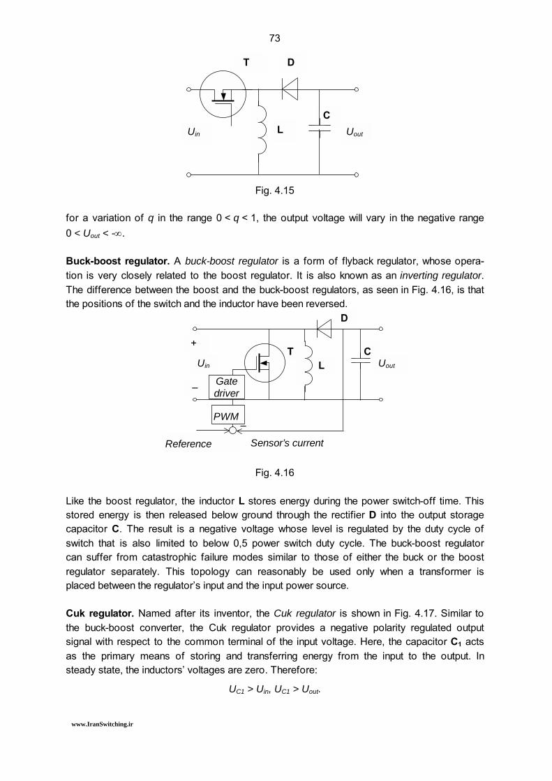
73
Fig. 4.15 for a variation of q in the range 0 < q < 1, the output voltage will vary in the negative range 0 < Uout < -∞. Buck-boost regulator. A buck-boost regulator is a form of flyback regulator, whose opera-tion is very closely related to the boost regulator. It is also known as an inverting regulator. The difference between the boost and the buck-boost regulators, as seen in Fig. 4.16, is that the positions of the switch and the inductor have been reversed.
Fig. 4.16
Like the boost regulator, the inductor L stores energy during the power switch-off time. This stored energy is then released below ground through the rectifier D into the output storage capacitor C. The result is a negative voltage whose level is regulated by the duty cycle of switch that is also limited to below 0,5 power switch duty cycle. The buck-boost regulator can suffer from catastrophic failure modes similar to those of either the buck or the boost regulator separately. This topology can reasonably be used only when a transformer is placed between the regulators input and the input power source. Cuk regulator. Named after its inventor, the Cuk regulator is shown in Fig. 4.17. Similar to the buck-boost converter, the Cuk regulator provides a negative polarity regulated output signal with respect to the common terminal of the input voltage. Here, the capacitor C1 acts as the primary means of storing and transferring energy from the input to the output. In steady state, the inductors voltages are zero. Therefore:
UC1 > Uin, UC1 > Uout.
D T
L C
Uin Uout
D
+
–
Sensor’s current Reference
T L
C
Gate driver
PWM
Uout Uin
www.IranSwitching.ir

74
Fig. 4.17
When the switch is off, the inductors currents flow through the diode D. The current IL1 de-creases because UC1 > Uin. The energy stored in L2 feeds the output. Therefore, IL2 also de-creases. When the switch is on, UC1 reverse biases the diode. The currents IL1, IL2 flow through the switch T. The capacitor C1 discharges through the switch and IL2 increases. The input feeds energy to L1 causing IL1 to grow. Thus, this circuit produces continuous current without any filters. Its uninterruptible output current reduces the required capacity of output capacitor. Summary. The most universal DC/DC converters step up and step down the load voltage, support single-, two- and four-quadrant operation, and do not require additional filters and powerful reactive elements. The powerful and fast switching devices are the necessary components of such circuits.
Uin
+
C1
– Sensor’s current
D T
L1
C2
Gate driver
PWM
Uout
L2
www.IranSwitching.ir

75
Part 5. Utility Circuits
5.1. Snubbers and Clamps
Functions and types. The switching of the loads with the reactive components,
such as a resistive-inductive load, has some particularities. These components store energy therefore the switch should withstand high current peaks or high voltage spikes. Due to the commutation transients, the signal shape is distorted and additional switching losses occur in the converters. In order to overcome the danger of overheating and overvoltages, semi-conductor switches are equipped with protection circuits and damping chains, so named snubber circuits.
The function of a snubber circuit is to reduce the electrical stresses placed on a power de-vice during switching to the levels that are within the rating of the device by the number of methods:
• limiting voltages applied to switch during turn-off process, • limiting the rate of voltages rise across switch during turn off, • limiting device currents and their rate of rise during turn-on transients, • limiting the rate of currents rise through devices at turn on, • shaping the switching trajectory of a device as it turns on and off.
From the circuit topology prospective, there are three broad classes of snubber circuits:
• unpolarized series RC snubbers used to protect diodes and thyristors by limiting the maximum voltage, its rate of rise, and reverse recovery,
• polarized RC snubbers used to shape the turn-off portion of the switching trajec-tory of switches, to clamp voltages applied to the devices or to limit their rate of rise during turn off,
• polarized LR snubbers used to shape the turn-on switching trajectory of switches and/or to limit current rating during device turn on.
There are situations, however, in which a protection circuit that limits the maximum voltage at the switch is needed. This special circuit is referred to as a voltage clamp.
Diode snubbers. Snubbers are needed in power diode circuits to minimize overvolt-ages. These overvoltages occur due to a stray or leakage inductance in series with the di-ode. A simple unpolarized snubber consists of a resistor in series with a capacitor connected across the diode as shown in Fig. 5.1. During the decay of reverse recovery current the ca-pacitor serves to limit the voltage spike. The energy stored in the inductance of the reverse recovery current loop serves to charge the capacitor, thereby reducing the spike. The resis-tor dissipates some of this energy, and, if suitably chosen, damps out oscillations in the cir-cuit. Preliminary capacity value of the snubber may be selected as 1 2 µF and resistance value is equal
√(L / C) < R < 2√(L / C)
www.IranSwitching.ir

76
where L is the inductance of the commutation current loop. The resistor power should be approximately calculated as follows: P = 450CU2 where U is the phase voltage. Fig. 5.1 Fig. 5.2 Thyristor snubbers. If the current in a thyristor rises at too high rate, the device can be de-stroyed. Some inductance must be present or inserted in series with the thyristor so that dI/dt is below a safe limit specified by the manufacturer (Fig. 5.2, a). A thyristor may turn on (without any gate pulse) if the forward voltage is applied too quickly. This is known as dU/dt turn on and it may lead to improper operation of the circuit. A simple RC snubber, as shown in Fig. 5.2, a, is normally used to limit dU/dt of applied forward voltage.
Simple polarized snubber circuit shown in Fig. 5.2, b, reduces turn-off voltage peaks. The resistor in the snubbing circuit is required for limiting the discharge current of the capacitor at turn on. Frequently, the resistor has a diode in parallel in order to make the capacitor more effective at limiting voltage rate in forward direction (Fig. 5.2, c). In thyristor switches, the forced commutation chains are used. For switching off a thyristor, the current should be reduced below the holding value by the specific closing circuitry be-tween the anode and cathode. This circuit contains a simple energy source capacitor, which directs current against the thyristor current. When the current through the thyristor is required to be switched off at a desired instant, it is momentary reverse biased by making the cathode positive with respect to anode. For this forced commutation, a commutation cir-cuit as shown in Fig. 5.3, a is used. Many forms of commutation circuits have been devel-oped to force-commutate thyristors. In most of them a preliminary charged capacitor is mo-mentarily connected across the conducting thyristor to reverse bias it. If the diode is reverse biased, its current falls, becomes zero, then reverses and becomes zero again. As an additional energy source, a commutation thyristor may be used. Fig. 5.3, b shows an example of the commutation circuit. When the auxiliary thyristor D2 is conducting, the ca-pacitor C charges up to the output voltage. After the capacitor has been charged, the thyris-tor D2 turns off. Ones the main thyristor D1 is switched on, the capacitor C discharges through the commutation circuit of the diode D3 and the coil L. Because of the coil induc-tance, the inverse current flows until the capacitor voltage equals to output voltage. The voltage of D1 becomes negative and D1 turns off. The capacitor charges through the load and D2 again and the process repeats.
a. b. c.
www.IranSwitching.ir

77
Fig. 5.3 Another example of a commutation circuit is shown in Fig. 5.3, c. This circuit is sometimes known as the McMurray commutation circuit. When the main thyristor D1 is on, the capacitor C is charged. To turn off the thyristor, the auxiliary thyristor D2 is fired. As a result, an oscilla-tory current pulse passes through L, C, D2, D1. This negative commutation current flows in a direction opposite to the load current already flowing through D1. When these currents be-come equal, the current through D1 falls to zero and D1 turnes off. GTO thyristor must have a snubber circuit also. A polarized snubber consisting of a diode, capacitor, and resistor (Fig. 5.4) is used for limiting the rate of voltage rise at turn off. More-over, during the fall time of the turnoff process, the device current is diverted (known as cur-rent snubbing) to the snubber capacitor (charging it up). Unlike the SCR, forward voltage is reapplied immediately after turning off in this circuit.
Fig. 5.4
Transistor snubbers. There are three basic types of snubbers for transistors:
• turn-off snubbers, • turn-on snubbers, • overvoltage snubbers.
The goal of the turn-off snubber is to provide minimum voltage across the transistor while the current turns off. Connecting a diode RC chain across the transistor as shown in Fig. 5.5, a can approach this purpose. Such polarized circuit provides a low voltage across the transistor while the current turns off. All the capacitor energy is dissipated in the resistor, which is easier to cool than the transistor. This circuit limits the peak current also.
Uin
+
−
a.
Commu-tation circuit
C
L D3
D2
b.
D1
D3
C D2
c.
D1
L
www.IranSwitching.ir

78
The overvoltage at turn off due to the stray inductances can be minimized by means of the polarized snubber circuit shown in Fig. 5.5, b. Polarized snubber shown in Fig. 5.5, c re-duces turn-on switching losses and limits the maximum currents. In addition, it reduces the voltage across the transistor as the current builds up.
Fig. 5.5 Polarized snubber, shown in Fig. 5.5, d is used with power transistor circuits with inductive load to avoid the simultaneous occurrence of peak voltage and peak current. If no snubber circuit is used and the base current is removed to turn off the transistor, the voltage across the device first rises, and when it reaches the dc supply voltage the collector current falls. The peaks of voltage and current occur almost simultaneously, and this may lead to secon-dary breakdown failure. When the snubber circuit is used and base current is removed to turn off the transistor, the collector current is diverted to the capacitor. The current, therefore, decreases as the collector-emitter voltage increases, avoiding the simultaneous occurrence of peak voltage and peak current. Again, the transistor has not reverse blocking capability hence it is shunted by anti-parallel diode if it is used in ac circuit. It should be mentioned that snubber arrangement for multi-device circuits differs in details from the configurations used to protect single devices. Voltage clamps. Voltage clamps are used exclusively for the avalanche (overvoltage) breakdown failure exclusion. This is when the voltage spike exceeds limits of the switch. The rectified diode and Zener diode clamps are used, as shown in Fig. 5.6, a, b. All Zener diodes begin conducting very quickly but it is not obviously in case of rectifier diodes. The variation of the voltage clamp is what could be called a soft clamp (Fig. 5.7, a, b). These clamps return the spikes energy to a soft current sink such as a capacitor. Fig. 5.8 shows the overvoltage protection of two IGBT connected in series. The resistors maintain steady-state voltage balance by compensating the differences in device leakage currents. Very fast transients are balanced by the capacitors, which can be much smaller than for a similar circuit using BJT or thyristors. During switching, differences in delay from one device to another will tend to lead to unbalanced voltages. The active clamp circuit, formed by the Zener string and IGBT limits UCE to a value above the Zener breakdown volt-age.
a. b. c. d.
www.IranSwitching.ir

79
Fig. 5.6 Fig. 5.7 Summary. Snubbers and clamps became the compulsory part of any power switch. They protect power diodes, thyristors, and transistors in switching operations and help them to withstand overvoltages and overcurrents.
Fig. 5.8
5.2. Gate and Base Drivers
Preliminary considerations. The primary goal of gate and base drivers is to switch
a power semiconductor device from the off state to the on state and vice versa. In most situations, a designer seeks low-cost driver circuit that minimizes the turn-on and turn-off times so that the device spends little time in traversing the active region where instantane-ous power dissipation is large. The functions of gate and base drivers are divided between control logic circuit and driver circuit. The first one is intended for:
• forming the main and auxiliary discrete intervals in accordance with the control logic of semiconductor devices;
b. a. b. a.
Uin
Uin
www.IranSwitching.ir

80
• producing the carrier signals; • generation the control pulses of the power devices.
The drive circuit is the interface between the control logic and the switching device. Its func-tions are as follows:
• shaping pulses length, amplitude, and waveform; • amplifying the control signals to levels required by driving switch; • distribution pulses among the power devices; • providing electrical isolation when required between the switch and logic-level
signal control circuits.
The basic topology of the drive circuit is dictated by its functional considerations:
• is the output signal unipolar or bipolar? • can the drive signals be directly coupled or electrically isolated? • is the output of the drive circuit connected in parallel with the switch or in series? • is the drive circuit implemented protection of the switch from extra stresses? • must the drive circuit provide a large output current (as for BJT) or large voltage
(as for FET)?
Thyristor control logic. In ac systems, an electronic controller influencing the phase of the firing pulses normally performs a thyristor switching on as shown in Fig. 5.9.
Fig. 5.9 The switching off is produced by means of natural commutation caused by cycling of the supply voltages. The control logic circuit compares the output signal Um of the controller with a saw-tooth periodic carrier signal Uc synchronized by the line voltage UA. For this purpose, the carrier signal generator G is used. Whenever the difference becomes positive for the first time in each half period, the monostable T produces a short pulse IG, which, after amplifica-tion, passes through an isolating circuit to the gate of the thyristor to be fired.
IG
Um
Um Uc
α α α
Uc –
ωt
UA
T Uin
G
ωt
www.IranSwitching.ir

81
It is seen that the comparison of the modulated signal with the carrier signal represents a sampling method, at the same time providing a voltage-to-phase conversion. If, instead of a saw-tooth function, alternations of cosine wave are employed, the control curve becomes a straight line, i.e. the system assumes constant voltage gain Ud / Um. The same effect is sometimes achieved by inserting an arcsine wave generator (Um = arcsin Uin) in the input channel of the firing circuit. For the control of multiphase rectifiers and inverters, the multi-channel pulse distribution sys-tem is required. Here, by the logical multiplication the chain of dual pulses is produced as shown in Fig. 5.10. The advantage of multi-channel pulse distribution system is the simplicity of the gate driver circuit and fast operation. With a dc supply, there is no natural commuta-tion available, and other methods of device switching off have to be employed.
Fig. 5.10 PWM transistor control logic. PWM is the most popular method providing the transistor control logic for inverters, AC/AC converters, and choppers. To obtain balanced three-phase output voltages in a three-phase PWM system, the triangle carrier voltage waveform is com-pared with three sinusoidal modulated voltages that are 2π/3 radians out of phase, as have been shown in Fig. 2.13. There, three sinusoidal waves present the voltage reference sig-nals and UU, UV, and UW are the output voltages of a converter. By such a way, voltage or current controller determines the firing instants for the transistors. The disadvantage of this method deals with the bipolar modulation, which leads to high cur-rent ripples and high reactive power produced by converter. In addition, the phase voltages become asymmetrical due to the constancy of the modulation frequency. Clearly, it results in a rising control error between the sinusoidal reference and the piecewise output current or voltage and must be taken into account when designing a control system.
UU, UV, UW
ωt
Uc
ωt
IG ωt ωt ωt ωt ωt ωt
www.IranSwitching.ir

82
Vectorial PWM transistor control logic. A very effective method that is particularly suited for fast switching converters is called vectorial PWM because it represents an attempt to re-produce in a given time interval a voltage vector demanded by a controller. Unlike PWM, this method implements the six-step block control system discussed during the inverters study-ing. For this purpose, a converter circuit shown in Fig. 2.9 is simulated by a switching model, shown in Fig. 5.11, a, where none of the legs is short-circulating the link voltage and each load terminal assumes a potential defined by the control.
Fig. 5.11 The timing diagram of the method corresponds that in Fig. 2.11. Here one transistor in each leg must be blocked while the other is conductive, except for the short protective intervals, where both transistors are blocked and the load current flows through one of the shunting diodes. To prevent short circuit condition, each half bridge is modeled by a reversing switch indicated by a binary variable Si = 1, 0, depending on whether the switch is in the upper or lower position. The switching state (S1, S2, S3) of the complete converter is then described by a three bit binary word having eight different values, including (1, 1, 1) and (0, 0, 0), called zero vector states, where the load terminals are short circuited at the upper or lower dc bus. The protective interval, which lasts only few microseconds, can be assigned to a fi-nite switching time in the converter model. When writing the voltage vector in terms of line-to-line voltages, six distinct voltage vectors and two zero vectors result, as seen in Fig. 2.11 and Fig. 5.11, b and in the table below:
U1 U2 U3 U4 U5 U6 U0, U7 Us 100 110 010 011 001 101 111, 000
UUs 2Ud / 3 Ud / 3 –Ud / 3 –2Ud / 3 –Ud / 3 Ud / 3 0 UVs –Ud / 3 Ud / 3 2Ud / 3 Ud / 3 –Ud / 3 –2Ud / 3 0 UWs –Ud / 3 –2Ud / 3 –Ud / 3 Ud / 3 2Ud / 3 Ud / 3 0
Clearly, when going from one corner of the hexagon to the next, only one leg of the con-verter needs to change its state. The voltage of each phase is equal to ±2Ud / 3, ±Ud / 3, or zero. Voltage vectors are oriented along the axes of phases U, V, W. The amplitude of the space vector is equal to Ud and during the voltage period it places one of the six positions.
D1
D2 D3
2Ud / 3
D5
D4
US3
US2
1
0 1
0
1
0 S3
S2
+
–
US1
a.
S1
Ud US2
US3
b.
D6
www.IranSwitching.ir

83
As a result, the vectors end travels on the hexagon or stops at zero. The vector paths de-viation from the circle corresponds to the voltage and current distortions. Compared to the PWM, vectorial PWM allows a higher phase voltage and thus a higher out-put power of a converter. The output voltage amplitude in PWM is Ud / 2. With the vectorial PWM, the amplitude is equal to the inner-circle radius of the hexagon, that is Ud / √ 3 or 15,5% higher than with PWM. However, this is achieved through abandoning the sinusoidal output that results in higher losses caused by higher harmonic components.
Driver circuits. Direct-coupled drivers with unipolar outputs are the simplest driver circuits. The block labeled IC in Fig. 5.12, a is an integrated circuit that provides a base current for the intermediate BJT T1 that drives the main BJT T2. Its inner timer establishes the switching frequency. The duty cycle is determined by the monostable delay, which sets the RC-circuit.
Fig. 5.12 Driving the gate of MOSFET is a process essentially similar to charging a capacitor. Be-cause the MOSFET will not turn on until the gate voltage riches its threshold value, driving the gate through a low impedance to minimize turn-on delay is important. A device that is particularly well suited to driving MOSFET is the integral circuit known as a MOS clock driver (Fig. 5.12, b). Thyristor and MOSFET gate drivers both must provide finite charge to the device that is a short pulse. However, whereas a negative gate current is required to turn off MOSFET, such current does little in turning-off thyristor. The notable exceptions are GTO and MCT. There-fore, a circuit as simple as that shown in Fig. 5.13 is often satisfactory for triggering a thyris-tor. The thyristor is turned on by a gate pulse, which can be obtained from a firing circuit. When the gate pulse is applied, anode current builds up and the voltage across the device falls. When the device is fully turned on, the voltage across it is quite small (typically 1 to 2,5 V) and for all practical purposes the device behaves as a short circuit. The device switches on very quickly, the turn-on time typically being 1 to 3 µs. The width of the gate pulse is in the range 10 to 50 µs with the amplitude in the range 20 to 200 mA. The gate resistor reduces sensitivity the turn-on process to noise. Direct-coupled drivers with unipolar outputs are only suitable for driving output devices at reasonably low switching frequencies. Direct-coupled
T2
T1
С
R UC
a.
UB
IC
Uin
Uin UG UD
b.
IC T2
www.IranSwitching.ir

84
drivers with bipolar outputs shown in Fig. 5.14 require split dc supplies and are capable of driving switches on and off rapidly. They are suitable for high switching frequencies but are restricted for driving the grounded switches.
Fig. 5.13 Fig. 5.14 Electrical isolation of drive circuits can be achieved by means of transformers or optocou-plers. Example is given in Fig. 5.9. In high voltage applications, such as dc transmission or static reactive power compensators, optical fibers may be used for transmitting the firing pulses, thus preventing electromagnetic interference. Summary. Gate and base drivers provide the operation of power electronic devices in power converters. Their design and principle of operation define the quality, cost, and reli-ability of power converter.
5.3. Electromagnetic Compatibility
EMI. The presence of unwanted voltages or currents in electrical equipment, which
can damage the system or degrade its performance, is called interference. A frequency spectrum of electromagnetic interference (EMI) covers a wide range from dc up to the GHz range. EMI frequencies of the radio spectrum 100 kHz to 100 MHz are known as radio fre-quency interference (RFI). EMI may be introduced into an electric circuit through the follow-ing paths:
• conducted over the power or signal cables by voltage dips, sags, swells, unbal-ance, harmonics, overvoltages, resonance oscillating, etc;
• radiated as electric fields with a high dU/dt and magnetic fields with a high dI/dt.
EMI covers the following main groups:
• conducted low frequency (LF) interference (up to about 10 kHz): voltage dips and power interruptions, voltage sags and swells, voltage unbalance, power fre-quency variations, dc in ac circuits and vice versa, harmonics in ac networks (up to approximately 3 kHz), coupled LF voltages and currents;
• radiated LF interference (up to about 10 kHz): electric fields with a high dU/dt and magnetic fields with a high dI/dt;
Uin
UA
+
− IC
UD
−VG
+UG
IC
www.IranSwitching.ir

85
• conducted high frequency (HF) interference (from 10 kHz to 1 GHz): transient overvoltage due to lightning or switching, oscillating transients due to resonance, coupling HF voltages and currents;
• radiated HF interference (from 10 kHz to 1 GHz): electric fields with a high dU/dt and magnetic fields with a high dI/dt;
One of the circuits, which participate in the interference, is the EMI source and another cir-cuit is the EMI receptor or EMI victim that is upset by the interference energy. There must be a coupling path between the source and the receptor. There are two main classes of EMI sources:
• natural events such as lightning, electrostatic and cosmic discharges, etc; • man-maid interference generated by equipment, commutation, and control appli-
cations.
The main artificial sources of EMI are:
• any circuit, which produces arcs; • circuits, which generate non-sinusoidal voltages, produce electric fields; • circuits, which generate non-sinusoidal currents, produce magnetic fields.
Any ac converter is a source of both conducted and radiated EMI. EMC. Electromagnetic compatibility (EMC) refers to the ability of equipment to function satis-factory without producing emissions that degrade the performance of other equipment and also are not affected by emissions from other equipment. The rapid growing of the use of non-linear power electronics devices has increased the overall level of EMI in industry. To compound the problem, there has been a rapid increase in the number of electronic control and communications devices, which operate at low voltages and high speeds and are sus-ceptible to this high level of interference. The digital control circuits, switch-mode power supplies, and other fast switching circuits can all contribute to emission. It is the power converter, which is an exceptionally strong source of emission because its fast changing output is connected directly to the external environ-ment. Fast changing pulse edges with typical rise times of the order of 50 100 ns contain significant energy up to about 30 MHz. This voltage is presented both between output phases and also as a common-mode voltage between phases and earth. It results in high-frequency current flowing to earth through the load capacitances. High-frequency current causes unexpected voltage drops. Harmonics suppression is a matter for the power electronic designer and suitable internal measures can keep such emission under control. There are three methods of reducing har-monic currents:
• the first of them is the installation of a choke and capacitors between the power supply and converter;
• the second is the use of a harmonic series LC filter tuned for particular frequen-cies close to the equipment;
• the third deals with the use of multiphase devices.
www.IranSwitching.ir

86
Reducing harmonics by chokes and capacitors. One of the most practical solutions is to install an inductance (choke) on the supply side of the power converter to effectively raise the inductive impedance between the converter and the power supply. The choke can be located internally on the dc link or connected externally at the input terminals of the con-verter. The input bulk capacitor is usually placed between the power supply and converter in case of dc power converter. Being relatively large in value, it has the responsibility of storing the high and low frequency energy required by the supply during each power cycle. It is usually made up of at least two capacitors, an electrolytic capacitor for the current harmonic compo-nents and a ceramic capacitor for the switching frequency harmonics. The input capacitor charges at low frequency and sources current over a much higher frequency range. A further measure, which reduces emission into both supply and load circuits is to fit a ferrite ring around the output cable power conductors. The ring fits around the power cores but not the earth. Reducing harmonics by filters. The most common types of harmonic filters used in indus-try are series LC filters with some damping resistance. Filters may be of relatively simple single-tuned construction, but are usually the more sophisticated, 2nd or 3rd order filters to provide a wider frequency band. The typical power supply system with filters is shown in Fig. 5.15.
Fig. 5.15
LC filter between the input line and the equipment usually serves a dual purpose. First, a tank circuit acts as a high frequency EMI filter, which reduces the conducted noise leaving the switching supply back into the input line giving a reduction of typically 30 dB in overall emission into the supply line. The low-pass cutoff frequency of this filter should be no higher than 2 or 3 times the supplys operating frequency. The capacitors must be safety types with voltage rating suited to the supply voltage with respect to earth. Values in the range 100 nF to 2,2 µF can be used. The second purpose of this stage is to add small impedance between the input line and the bulk input capacitor (if presents). It reduces any transient voltages, spikes or surges. The filter specified by the load manufacturer should be used, and any lim-its on cable length or capacitance and on switching frequency adhered to.
input EMI filter bulk capacitor output choke
Uout Uin
electronic converter
www.IranSwitching.ir

87
The output LC filter section is called a choke filter. In case of ac load, it is a series inductor. In case of dc load, it is a series inductor followed by a shunt capacitor. Its purpose is to store energy for the load during the times when the power switches are non-conducting. It basi-cally operates like an electrical equivalent of a mechanical flywheel. The main problem with harmonic filters is that they can become detuned over a period of time due to age, tempera-ture or failure changes in the filter capacitance, changes in the inductance due to tempera-ture or current, and small changes in the system frequency. Reducing harmonics by multi-pulse converters. The use of converters of higher pulse numbers will greatly reduce the lower order harmonics. The frequencies of high order har-monics increase, therefore the shapes of input and output current approach to sinusoidal waveforms. Alternately, two converters of lower pulse numbers can be combined with a phase shift of π/6 radians to produce a system of higher pulse numbers. When several simi-lar controlled converters are connected to the same bus, as shown in Fig. 5.16, some can-cellation of harmonic currents takes place due to phase shifts between the firing angle of converters running of different speeds.
Fig. 5.16
Standards. The management of EMC falls into two categories:
• the establishment of standards for the containment of EMI by setting maximum limits on emission from equipment;
• the establishment of standards for the immunity of electronic devices, which will enable them to operate within interference.
The leading idea of all EMC related standards and regulations is that the product must have a certain level of immunity and the emitted interference level of the product should be below some rated limit. There are a great number of different standards covering all aspects of
Uout Uin
electronic converter 1
electronic converter 2
www.IranSwitching.ir

88
EMC: conducted or radiated emissions, electrostatic discharge, electromagnetic field, elec-trical transients, line harmonics, and mains dips are just a few to mention. The International Electromechanical Commission (IEC) has established the IEC 61000 series of standards to cover EMC requirements. In European Union, the requirements for emission and for immunity derive from the EMC Directive 89/336/EEC, which delegates the actual limits for specific standards. There are generic standards as well as product specific standards. In generic EMC standards, only two types of environments are defined:
• residential, commercial, and light industrial standards; • industrial standards.
Product family standards and product specific standards override generic requirements if such standards exist. If there is no product family standard, one should follow the suitable generic or general standard, which in turn refers to different basic standards. The baseline of European EMC standards is, that the basic standards describe the test pro-cedures, and in some cases test instrumentation and calibration techniques, while most specific application standards usually define limits, severity levels, and compliance criteria. The EU EMC standardization field utilizes a range of standards produced by various national and international bodies, such as IEC, CISPR (International Specific Committee on Radio Interference), ETSI (European Telecommunications Standards Institute), and CENELEC (European Committee for Electromechanical Standardization). General frequency ranges of EMC are defined in CISPR 16-1:
• band A 9 kHz to 150 kHz; • band B 0,15 MHz to 30 MHz; • band C 30 MHz to 300 MHz; • band D 300 MHz to 1 GHz.
Summary. To minimize the harmful influence of power converters on devices and people, the converters must satisfy EMC requirements, national, and international standards. Only such converters may be used in industry, business, and domestic applications.
www.IranSwitching.ir

89
Part 6. Experiments Using Electronics Workbench
6.1. Objective
Procedure. The practice includes a set of exercises in power electronics meant for Miltisim from Electronics Workbench software. The exercises tasks are:
• power electronics circuits development and calculation, • selection of electronic components, • schematic building, • voltages and currents measuring, • voltage and current waveforms analyzing, • results explanation and documentation.
At the end of each exercise, compare calculated and experimental data. A report should in-clude:
• experimental circuit diagram, • resulting and comparative data tables, • voltage and current traces with indication of axes scales, • dependencies diagrams, • conclusions with result explanation.
Required Components and Instruments
• Sources: ground, dc voltage source, ac current source, voltage-controlled volt-age source, current-controlled voltage source, pulse voltage source, clock source.
• Basic: resistor and potentiometer, capacitor, inductor and variable inductor, switch and voltage-controlled switch.
• Diodes: diode, full-wave bridge rectifier, silicon-controlled rectifier (SCR). • Transistor: 3-terminal enhancement n-MOSFET. • Analog IC: 3-terminal opamp. • Indicators: voltmeter, ammeter. • Miscellaneous: buck converter, boost converter, buck-boost converter. • Instruments: oscilloscope, function generator.
Reference Data
• Load power Pd = 10 W to 100 kW. • Load resistance Rd = 1 Ω to 100 kΩ. • Supply frequency f = 50 Hz.
www.IranSwitching.ir

90
6.2. Single-Phase Half-Wave Rectifiers
Exercise 1.1. Simple M1 rectifier
1. To begin with, draw and build the schematic using the only 4 components: ac voltage source, diode, resistor, and ground:
• connect the positive pin of the voltage source to the diode anode and ground its negative pin,
• then connect the load between the diode cathode and ground.
2. Add an oscilloscope and connect it for viewing the load voltage Ud.
3. Activate the circuit simulation and view result. Tune the oscilloscope settings either be-fore or during simulation.
4. For viewing the load current, add the current-controlled voltage source in series with the load resistor and connect it to the oscilloscope. Tune the oscilloscope and view both sig-nals: the load voltage and current.
Exercise 1.2. M1 rectifier with resistive load
1. Calculate the required average load voltage Ud and load current Id using the Ohms low.
2. Calculate the required rms supply voltage as follows:
Us = πUd / √2.
3. Calculate the peak inverse voltage, PIV (also called reverse breakdown voltage, BV) of the diode as follows:
PIV = πUd.
4. In the circuit of Exercise 1.1, assign values Us, f, Rd and select the diode model from the library.
5. For measuring average voltage Ud and current Id, add a dc voltmeter across the load and a dc ammeter in series with the load. Also, connect the oscilloscope for viewing the load voltage Ud.
6. For viewing the diode inverse voltage, add the voltage-controlled voltage source across the diode and connect it to other channel of oscilloscope.
7. After activating the circuit, tune the oscilloscope and view both signals: load voltage and diode inverse voltage.
Exercise 1.3. M1 rectifier with LC filter
1. In the circuit of Exercise 1.2, measure the peak-to-peak ripple voltage Ur and calculate the ripple factor of the output waveform as follows:
r = Ur / (2Ud).
2. Calculate the power factor of the circuit as follows:
cos ϕ = Pd / S = π2 / (2√2).
www.IranSwitching.ir

91
3. For experimental measuring the power ratio, add an ac ammeter in series with the diode and ac voltmeter across the ac voltage source. After activating the circuit, measure Us, Is, Ud, Id, and calculate cos ϕ with S = Us⋅Is and Pd = Ud⋅Id.
4. For tenfold lowering the ripple factor (rC = r / 10), add an LC filter built on a capacitor across the load resistor and a reactor in series with the diode and calculate filter parame-ters (H⋅µF) as follows:
LC = 10⋅(r / rC + 1)
5. After activating the circuit, measure Us, Is, Ud, Id, and calculate the new value of power factor. Measure the maximum Udmax and minimum Udmin rectified voltages and its average value Ud and calculate the actual ripple and power factors as follows:
rC = (Udmax Udmin) / (2Ud), cos ϕ = Pd / S.
Exercise 1.4. M1 rectifier with inductive load
1. Build an M1 rectifier circuit with ac voltage source, diode, resistor, and ground. Place the oscillator and connect it to view the load voltage and load current. Also, add the indicators for measuring the load voltage and current. Assign the reference values and select the diode model as in previous exercises.
2. Build an inductive load by adding an inductor L = 50 to 500 mH in series with the load re-sistor.
3. After activating the circuit, view, explain, and document the result.
4. To compensate the inductance, add the same LC filter as in Exercise 1.3 and fine-tune the circuit.
Exercise 1.5. M1 thyristor rectifier
1. Build the schematic using ac voltage source, thyristor (SCR), resistor, pulse voltage source, and ground:
• connect the positive pin of the voltage source to the thyristor anode and ground its negative pin,
• then connect the load between the thyristor cathode and ground • connect the pulse voltage source to the thyristor gate and ground it.
2. Place the oscillator and connect it to view the load voltage and current. Also, add the in-dicators for measuring the load voltage and current.
3. Calculate the required rms supply voltage Us and assign the values of Us, f, Rd and the pulse voltage sources Period T = 1 / f.
4. After activating the circuit, view the signals. Use the pulse voltage source as a firing regu-lator by changing its Delay time. To reduce the firing angle, set delay near zero. To enlarge the angle, raise the delay up to T / 2.
5. Change the firing angle from 0 to 180 degrees, measure the load voltage, write it into a table, and build the control curve that is the diagram of the load voltage versus firing an-gle. Explain, and document the result.
www.IranSwitching.ir

92
6.3. Single-Phase Full-Wave Rectifiers
Exercise 2.1. Simple M2 rectifier
1. Build the schematic using function generator, 2 diodes, resistor, and ground:
• connect the positive and negative terminals of the function generator to the di-odes anodes,
• join the cathodes and the load input together, • ground the load output and the common terminal of the function generator.
2. Add an oscilloscope and connect it for viewing the load voltage Ud. For viewing the load current, add the current-controlled voltage source in series with the load resistor and connect it to the oscilloscope. For measuring the average voltage Ud and current Id, add a dc voltmeter across the load and a dc ammeter in series with the load.
3. Calculate the required average load voltage Ud and load current Id using the Ohms low.
4. Calculate the rms supply voltage of each half-winding as follows:
Us = πUd / (2√2).
5. Assign the reference values: Us, f, Rd.
6. Activate the circuit simulation, measure the load voltage and current, and view both sig-nals: voltage and current. Tune the oscilloscope settings either before or during simula-tion.
Exercise 2.2. M2 rectifier with LC filter
1. Calculate the peak inverse voltage of the diode as follows:
PIV = πUd.
In practice, this value will be some less due to the diode direct voltage drop UA.
2. Measure the peak-to-peak ripple voltage Ur and calculate the ripple factor of the output waveform as follows:
r = Ur / (2Ud).
3. For tenfold lowering the ripple factor (rC = r / 10), add an LC filter built on a capacitor across the load resistor and a reactor in series with the diode and calculate filter parame-ters (H⋅µF) as follows:
LC > 2,5⋅(r / rC + 1)
4. After activating the circuit, measure the maximum Udmax and minimum Udmin rectified volt-ages and its average value Ud and calculate the actual ripple factor as follows:
rC = (Udmax Udmin) / (2Ud).
www.IranSwitching.ir

93
Exercise 2.3. M2 Thyristor rectifier
1. Build the same schematic as in Exercise 2.1 using thyristors instead of diodes.
2. Build the simple gate driver using a pulse voltage source. Connect the pulse voltage source between the thyristors gates and ground. Set its Period = 1 / (2f) and Pulsed value near 2 V.
3. After activating the circuit, view the signals. Use the pulse voltage source as a firing regu-lator by changing its Delay time. To reduce the firing angle, step down the delay and raise it to enlarge the angle.
5. After activating the circuit, view, explain, and document the result. Then, change the load resistance from 10 to 1000 Ω and build the load curve that is the diagram of the load volt-age versus load current.
6. Build an inductive load by adding an inductor with L = 100 to 1000 mH in series with the load resistor.
7. After activating the circuit, view, explain, and document the result. Again, change the load resistance and build the new load curve.
Exercise 2.4. Simple B2 bridge rectifier
1. Build the schematic using firstly only 4 components: ac voltage source, full-wave bridge rectifier, resistor, and ground:
• connect the bridge rectifier inputs to the voltage source, • connect the bridge rectifier outputs to the load, • ground the load.
2. Calculate the required average load voltage Ud and load current Id using the Ohms low.
3. Calculate the required rms supply voltage as follows:
Us = πUd / (2√2).
4. Assign the reference values: Us, f, Rd.
5. Add an oscilloscope and connect it for viewing the load voltage Ud. For viewing the load current, add the current-controlled voltage source in series with the load resistor and connect it to the oscilloscope also.
6. For measuring the average voltage Ud and current Id, add a dc voltmeter across the load and a dc ammeter in series with the load in the previous circuit.
7. Activate the circuit simulation, tune the oscilloscope, and view the load voltage and load current.
Exercise 2.5. B2 rectifier with LC filter
1. For measuring the rms voltage Us and current Is, add an ac voltmeter across the voltage source and an ac ammeter in series with the voltage source.
2. Measure the peak-to-peak ripple voltage Ur and calculate the ripple factor of the output waveform as follows:
www.IranSwitching.ir

94
r = Ur / (2Ud)
3. Calculate the theoretical power factor of the circuit as follows:
cos ϕ = (2√2) / π
4. After activating the circuit, measure Us, Is, Ud, Id, and calculate the experimental power factor Pd / S. Compare the calculated and experimental results.
5. For tenfold lowering the ripple factor (rC = r / 10), add an LC filter built on a capacitor across the load resistor and a reactor in series with the diode and calculate filter parame-ters (H⋅µF) as follows:
LC = 2,5⋅(r / rC + 1)
6. After activating the circuit, measure Us, Is, Ud, Id, and calculate the new power factor:
cos ϕ = Ud⋅Id / (Us⋅Is)
7. Measure the maximum Udmax and minimum Udmin rectified voltages and calculate the ac-tual ripple factor as follows:
rC = (Udmax Udmin) / (2Ud)
Exercise 2.6. B2 rectifier with inductive load
1. Build the same B2 rectifier circuit as in Exercise 2.5.
2. Build an inductive load by adding a variable inductor L = 50 to 500 mH in series with the load resistor.
3. After activating the circuit, view, explain, and document the result. Measure the peak-to-peak ripple voltage Ur and the phase shift between the load voltage and current. Build the diagram of the ripple voltage versus an inductance.
4. To compensate the phase shift, add a capacitor across the inductor and find experimen-tally the capacitance for tenfold lowering the ripple factor.
Exercise 2.7. B2 thyristor rectifier
1. Build the schematic using ac voltage source, 4 thyristors D1, D2, D1, and D2, resistor, pulse voltage source, and ground:
• connect the positive pin of the voltage source to the D1 anode and D2 cathode, • connect the negative pin of the source to the D2 anode and D1 cathode, • connect the load resistor between the joint cathodes of D1 and D2 and the
ground, • also, ground the joint anodes of D1 and D2.
2. Add an oscilloscope and connect it for viewing the load voltage Ud. For viewing the load current, add the current-controlled voltage source in series with the load resistor and connect it to the oscilloscope also.
3. For measuring the average voltage Ud and current Id, add a dc voltmeter across the load and a dc ammeter in series with the load.
www.IranSwitching.ir

95
4. Calculate the required average load voltage Ud and load current Id using the Ohms low. Calculate the required rms supply voltage and assign the reference values: Us, f, Rd.
5. Build the gate driver using pulse voltage source, which Period is 1 / (2f) and Pulse width 1 to 5 ms. Connect its positive pin to the SCR gates and ground the negative pin.
6. After activating the circuit, view the signals and measure the load voltage and current. Use the pulse voltage sources as firing regulators by changing its Delay time.
6.4. Three-Phase Rectifiers
Exercise 3.1. Simple M3 rectifier
1. Build the schematic using firstly 3 ac voltage sources U, V, and W, 3 diodes, resistor, and ground:
• ground the negative poles of the sources, • connect the load resistor between the joint diodes cathodes and the ground.
2. Add an oscilloscope and connect it for viewing the load voltage Ud.
3. For viewing the load current, add the current-controlled voltage source in series with the load resistor and connect it to the oscilloscope.
4. For measuring average voltage Ud and current Id, add a dc voltmeter across the load and a dc ammeter in series with the load.
5. Calculate the required average load voltage Ud and load current Id using the Ohms low.
6. Calculate the required rms supply voltage as follows:
Us = 2πUd / (3√2√3).
7. Assign the reference values: Us, f, Rd. Set the necessary phase shifts of each voltage source: 0 degrees for U, 240 degrees for V, and 120 degrees for W.
8. Activate the circuit simulation, tune the oscilloscope settings, and view result.
Exercise 3.2. M3 thyristor rectifier
1. Build the same circuit as in Exercise 3.1 using 3 thyristors DU, DV, and DW instead of di-odes.
2. Build a gate driver using the pulse voltage source between the thyristors gates and ground. Set the pulse voltage sources Period 1 / (3f) and Pulse width 1 to 3 ms
3. After activating the circuit, view the signals and measure the load voltage and current. Use the pulse voltage sources as firing regulator by changing its Delay time.
Exercise 3.3. Simple B6 rectifier
1. Build the schematic using firstly 3 ac voltage sources, 6 diodes, and resistor. Join the negative poles of the three voltage sources U, V, and W and connect the positive pin of each source to the corresponding pair of diodes:
• source U to the DU anode and DU cathode, • source V to the DV anode and DV cathode,
www.IranSwitching.ir
96
• source W to the DW anode and DW cathode.
Connect the load resistor between the joint cathodes of DU, DV, and DW and the ground. Also, ground the joint anodes of DU, DV, and DW.
2. Add an oscilloscope and connect it for viewing the load voltage Ud.
3. For viewing the load current, add the current-controlled voltage source in series with the load resistor and connect it to the oscilloscope.
4. For measuring average voltage Ud and current Id, add a dc voltmeter across the load and a dc ammeter in series with the load.
5. Calculate the required average load voltage Ud and load current Id using the Ohms low.
6. Calculate the required rms supply voltage as follows:
Us = πUd / (3√2√3).
7. Assign the reference values: Us, f, Rd. Set the necessary phase shifts of each voltage source: 0 degrees for U, 120 degrees for V, and 240 degrees for W.
8. Activate the circuit simulation and view result. Tune the oscilloscope settings either be-fore or during simulation.
Exercise 3.4. B6 thyristor rectifier
1. Build the same circuit as in Exercise 3.3 using 6 thyristors instead of diodes.
2. Build a gate driver using the pulse voltage source between the thyristors gates and ground. Set the pulse voltage source Period 1 / (3f) and Pulse width 1 to 3 ms
3. After activating the circuit, view the signals and measure the load voltage and current.
6.5. AC Converters
Exercise 4.1. Single-phase voltage regulators
1. Build the schematic using ac voltage source, voltage-controlled switch, load resistor, pulse voltage source, and ground:
• connect the positive pin of the voltage source to the voltage-controlled switch and ground its negative pin,
• then connect the load between the voltage-controlled switch and ground, • at last, insert the pulse voltage source between the positive controlling terminal
of the voltage-controlled switch and ground.
2. Assign the values Us, f, Rd in accordance with the reference data. In pulse voltage source set Period = 1 / (2f) and Pulse width < Period.
3. Add an oscilloscope and connect it for viewing the load voltage Ud. For viewing the load current, add the current-controlled voltage source in series with the load resistor and connect it to the oscilloscope. For measuring rms load voltage Ud and current Id, add an ac voltmeter across the load and ac ammeter in series with the load.
www.IranSwitching.ir

97
4. After activating the circuit, view the signals and measure the load voltage and current. Use the pulse voltage source Delay time and Pulse width options as switching regulation options by simultaneous changing their values as follow:
Period = Delay time + Pulse width.
5. By changing these options, build the diagram of the load rms voltage versus delay.
6. Replace the voltage-controlled switch with a pair of thyristors connected back-to-back. Build the own gate driver for each thyristor placing pulse voltage sources with Pe-riod = 1 / (2f) between the gate and cathode.
7. After activating the circuit, view the signals and measure the load voltage and current. Again, build the diagram of the load voltage versus the firing angle. Then, set the firing angle to 45 degrees, vary the load resistance from 1 Ω to 1 kΩ, and build the load curve (load rms voltage versus current) of the system.
Exercise 4.2. Single-Phase Bridge Inverters
1. Build the schematic using dc voltage source, 4 voltage-controlled switches S1, S2, S1, and S2, pulse voltage source, resistor, and ground:
• connect the positive pin of the dc voltage source to S1 and S2 upper terminals, • connect the negative pin of the dc voltage source to the S2 and S1 lower termi-
nals, • connect the load resistor between the joint S1 and S2 terminals and the joint S1
and S2 terminals, and ground them.
2. Add an oscilloscope and connect it for viewing the load voltage Ud. For viewing the load current, add the current-controlled voltage source in series with the load resistor and connect it to the oscilloscope also. For measuring the rms voltage Ud and current Id, add an ac voltmeter across the load and ac ammeter in series with the load. Assign the refer-ence values: Us, f, Rd. Set the on-state resistance of the switch to minimum allowable value.
3. Build a gate driver using 2 pulse voltage sources:
• connect the positive terminal of the first pulse voltage source to the positive con-trolling terminals of the voltage-controlled switches S1, S1,
• connect the positive terminal of the second voltage source to the positive control-ling terminals of the voltage-controlled switches S2, S2,
4. In both pulse voltage sources, set Period = 1 / f and Pulse width < Period / 2. In the sec-ond pulse voltage source, set Delay time = Period / 2
5. After activating the circuit, view the ac signals and measure the ac load voltage and cur-rent. Change the load frequency by simultaneous varying Period option of both pulse voltage sources and Delay time of the second pulse voltage source. Change the load voltage by simultaneous varying the Pulse width option of both pulse voltage sources. Build the diagram of the load rms voltage versus duty cycle:
Duty cycle = 2 Pulse width / Period.
www.IranSwitching.ir

98
6. Replace the voltage-controlled switches with 3-terminal enhancement n-MOSFETs. After activating the circuit, view the ac signals and measure the ac load voltage and current. Build the diagram of the load voltage versus duty cycle. Then, set the duty cycle to 50%, vary the load resistance from 10 Ω to 10 kΩ, and build the load curve of the MOSFET system.
Exercise 4.3. Voltage source and current source inverters
1. To build a voltage source inverter with ideal switches, use the same schematic as in Ex-ercise 4.2 without gate driver. Connect an oscilloscope, ac voltmeter, and ammeter.
2. Build a new gate driver using a function generator, comparator, and ground:
• set the function generator options as follows: square Waveform, Frequency 50 Hz, Duty Cycle 50%, Amplitude 1 - 10 V, Offset 0,
• connect the function generator positive terminal to the positive controlling termi-nals of the voltage-controlled switches S1, S1 and comparators negative input,
• ground the function generator common terminal, negative controlling terminals of each switch, and comparators positive input,
• connect the opamp output to the positive controlling terminals of the voltage-controlled switches S2, S2,
3. After activating the circuit, view the signals and measure the load voltage and current. Change the load frequency by varying the function generator Frequency. Change the load voltage by varying the function generator Duty Cycle option. Build the diagram of the load voltage versus duty cycle.
4. Replace the voltage-controlled switches with 3-terminal enhancement n-MOSFETs. After activating the circuit, view the signals and measure the load voltage and current. Build the diagram of the load voltage versus duty cycle. Then, set duty cycle to 50%, vary the load resistance from 10 Ω to 10 kΩ, and build the load curve of the MOSFET system.
5. To build a current source inverter, replace the dc voltage source with a dc current source and repeat the experiment. Change the load current by varying the function generator Duty Cycle option. Build the diagram of the load current versus duty cycle.
Exercise 4.4. Frequency converters
1. Build the same voltage source inverter with ideal switches as in Exercise 4.3.
2. Replace the dc voltage source with the simple bridge rectifier of Exercise 2.4:
• connect the full-wave bridge rectifier inputs to the ac voltage source, • connect the rectifier outputs to S1 and S2 upper terminals and S2 and S1 lower
terminals, • ground the negative terminal of the voltage source.
3. Assign the reference values: Us, f, Rd. Set the function generator options as follows: rec-tangle Waveform, Frequency <50 Hz, Duty Cycle 50%, Amplitude 1 - 10 V, Offset 0.
4. After activating the circuit, view the signals and measure the load voltage and current. Change the load frequency by varying the function generator Frequency. Change the load voltage by varying the voltage source Voltage.
www.IranSwitching.ir

99
5. Replace the voltage-controlled switches with 3-terminal enhancement n-MOSFETs. After activating the circuit, view the signals and measure the load voltage and current. Set Duty Cycle to 50%, vary the load resistance from 10 Ω to 10 kΩ, and build the load curve of the MOSFET system.
6. Insert a little inductive filter in series with the load. Tune the circuit, view the signals, and measure the load voltage and current.
6.6. Choppers
Exercise 5.1. Step-down choppers
1. Build the schematic using dc voltage source, voltage-controlled switch, load resistor, ca-pacitor, inductor, diode, and ground:
• connect the positive pin of the dc voltage source to the voltage-controlled switch and ground its negative pin,
• connect the inductor and cathode of the flywheel diode to other terminal of the switch and ground the diode anode,
• connect the capacitor and the load to other terminal of the inductor and ground them also.
2. Calculate the required load voltage Ud and load current Id using the Ohms low. Assign referenced value of Rd and Us = 2Ud.
3. Add an oscilloscope and connect it for viewing the load voltage Ud. For viewing the load current, add the current-controlled voltage source in series with the load resistor and connect it to the oscilloscope. For measuring the load voltage Ud and current Id, add a dc voltmeter across the load and dc ammeter in series with the load.
4. Build a gate driver, which Frequency value is near 5 kHz.
5. After activating the circuit, view the signals and measure the load voltage and current. Find the filter properties for tenfold lowering the rms current and voltage. Use the gate driver duty cycle as a switching regulator by changing its value from 0 to 100%. To re-duce the load voltage, set the minimum value; to step up the voltage, raise the value. Build the diagram of the load voltage versus duty cycle.
6. Replace the voltage-controlled switch with the 3-terminal enhancement n-MOSFET. After activating the circuit, view the signals and measure the load voltage and current. Build the diagram of the load voltage versus duty cycle. Then, set duty cycle to 50%, vary the load resistance from 10 Ω to 10 kΩ, and build the load curve of the MOSFET system.
Exercise 5.2. Closed-loop buck chopper
1. Build the schematic using dc voltage source S1, buck converter, load resistor, and ground:
• connect the buck converter between the positive pin of the dc voltage source and the load resistor,
• ground the negative pin of the dc voltage source and the load.
www.IranSwitching.ir

100
2. Calculate the required load voltage Ud and load current Id using the Ohms low. Assign referenced value of Rd and Us = 2Ud.
3. Add an oscilloscope and connect it for viewing the load voltage Ud. For viewing the load current, add the current-controlled voltage source in series with the load resistor and connect it to the oscilloscope. For measuring the load voltage Ud and current Id, add a dc voltmeter across the load and dc ammeter in series with the load.
4. Build a gate driver using the dc voltage source S2, which Voltage value is near 0,5 V. Connect its positive pin to the control terminal of the buck converter and ground the nega-tive pin.
5. After activating the circuit, view the signals and measure the load voltage and current. Then, vary the load resistance from 10 Ω to 10 MΩ and build the load curve that is the diagram of the load voltage versus load current.
6. To stabilize the load voltage, rebuild the gate driver and arrange the negative close loop:
• set the dc voltage source S2 Voltage value to Ud, • connect the dc voltage source S2 negative pin to the control terminal of the buck
converter and negative pin to the load.
7. After activating the circuit, measure the load voltage and current. Again, vary the load re-sistance from 10 Ω to 10 kΩ and build the load curve of the closed loop system.
Exercise 5.3. Step-up choppers
1. Build the schematic using dc voltage source, voltage-controlled switch, load resistor, di-ode, capacitor, inductor, and ground:
• connect the positive pin of the dc voltage source to the inductor and ground its negative pin,
• connect the voltage-controlled switch and the diode anode to other terminal of the inductor and ground the switch,
• then connect the capacitor and the load to the diode cathode and ground them also.
2. Assign the values Us and Rd in accordance with the reference data. Set the on-state re-sistance of the switch to minimum allowable value.
3. Add an oscilloscope, current-controlled voltage source, ac voltmeter, and ammeter as in Exercise 5.1.
4. Build the same gate driver as in Exercise 5.1.
5. After activating the circuit, view the signals and measure the load voltage and current. Find the filter properties for tenfold lowering the rms current and voltage. Use the gate drivers duty cycle for changing the load voltage. Build the diagram of the load voltage versus duty cycle.
6. Replace the voltage-controlled switch with the 3-terminal enhancement n-MOSFET. Set the clock Voltage value significantly more than Us. After activating the circuit, view the signals and measure the load voltage and current. Build the diagram of the load voltage
www.IranSwitching.ir

101
versus duty cycle. Then, set duty cycle to 50%, vary the load resistance from 10 Ω to 10 kΩ, and build the load curve of the MOSFET system.
Exercise 5.4. Closed-Loop Boost Chopper
1. Build the schematic using dc voltage source S1, boost converter, load resistor, and ground:
• connect the boost converter between the positive pin of the dc voltage source and the load resistor,
• ground the negative pin of the dc voltage source and the load.
2. Calculate the required load voltage Ud and load current Id using the Ohms low. Assign referenced value of Rd and Us = Ud / 2.
3. Add an oscilloscope and connect it for viewing the load voltage Ud. For viewing the load current, add the current-controlled voltage source in series with the load resistor and connect it to the oscilloscope. For measuring the load voltage Ud and current Id, add a dc voltmeter across the load and dc ammeter in series with the load.
4. Build a gate driver using the dc voltage source S2, which Voltage value is near 0,5 V. Connect its positive pin to the control terminal of the boost converter and ground the negative pin.
5. After activating the circuit, view the signals and measure the load voltage and current. Then, change the load resistance from 10 Ω to 10 MΩ and build the load curve that is the diagram of the load voltage versus load current.
6. To stabilize the load voltage, rebuild the gate driver and arrange the negative close loop:
• set the dc voltage source S2 Voltage value to Ud, • connect the dc voltage source S2 negative pin to the control terminal of the boost
converter and negative pin to the load.
7. After activating the circuit, measure the load voltage and current. Again, change the load resistance from 10 Ω to 10 kΩ and build the load curve of the closed loop system.
Exercise 5.5. Step-down and step-up choppers
1. Build the schematic using dc voltage source, voltage-controlled switch, load resistor, di-ode, capacitor, inductor, and ground:
• connect the positive pin of the dc voltage source to the voltage-controlled switch and ground its negative pin,
• connect the inductor and the diode cathode to other terminal of the voltage-controlled switch and ground the inductor,
• then connect the capacitor and the load to the diode anode and ground them also.
2. Assign the values Us and Rd in accordance with the reference data. Set the on-state re-sistance of the switch to minimum allowable value.
3. Add an oscilloscope, current-controlled voltage source, ac voltmeter, and ammeter as in Exercise 5.1.
www.IranSwitching.ir

102
4. Build the same gate driver as in Exercise 5.1.
5. After activating the circuit, view the signals and measure the load voltage and current. Find the filter properties for tenfold lowering the rms current and voltage. Use the gate drivers duty cycle for changing the load voltage. Build the diagram of the load voltage versus duty cycle.
6. Replace the voltage-controlled switch with the 3-terminal enhancement n-MOSFET. Set the clock Voltage value significantly more than Us. After activating the circuit, view the signals and measure the load voltage and current. Build the diagram of the load voltage versus duty cycle. Then, set duty cycle to 50%, vary the load resistance from 10 Ω to 10 kΩ, and build the load curve of the MOSFET system.
Exercise 5.6. Closed-loop buck-boost chopper
1. Build the schematic using dc voltage source S1, buck-boost converter, load resistor, and ground:
• connect the buck-boost converter between the positive pin of the dc voltage source and the load resistor,
• ground the negative pin of the dc voltage source and the load.
2. Calculate the required load voltage Ud and load current Id using the Ohms low. Assign referenced value of Rd and Us = Ud.
3. Add an oscilloscope and connect it for viewing the load voltage Ud. For viewing the load current, add the current-controlled voltage source in series with the load resistor and connect it to the oscilloscope. For measuring the load voltage Ud and current Id, add a dc voltmeter across the load and dc ammeter in series with the load.
4. Build a gate driver using the dc voltage source S2, which Voltage value is near 0,5 V. Connect its negative pin to the control terminal of the boost converter and ground the positive pin.
5. After activating the circuit, view the signals and measure the load voltage and current. Then, change the load resistance from 50 Ω to 50 kΩ and build the load curve that is the diagram of the load voltage versus load current.
6. To stabilize the load voltage, rebuild the gate driver and arrange the negative close loop:
• set the dc voltage source S2 Voltage value to Ud, • connect the dc voltage source S2 negative pin to the control terminal of the boost
converter and negative pin to the load.
7. After activating the circuit, measure the load voltage and current. Again, change the load resistance from 10 Ω to 10 kΩ and build the load curve of the closed loop system.
Exercise 5.7. Cuk choppers
1. Build the schematic using dc voltage source, voltage-controlled switch, load resistor, di-ode, capacitor, 2 inductors, and ground:
• connect the positive pin of the dc voltage source to the first inductor and ground its negative pin,
www.IranSwitching.ir

103
• connect the voltage-controlled switch and the capacitor to other terminal of the inductor and ground the switch,
• then connect the diode anode and the second inductor to other terminal of the capacitor and ground the diode cathode
• at last, connect the load to other terminal of the second inductor and ground it also.
2. Assign the values Us and Rd in accordance with the reference data. Set the on-state re-sistance of the switch to minimum allowable value.
3. Add an oscilloscope, current-controlled voltage source, ac voltmeter, and ammeter as in Exercise 5.1.
4. Build the same gate driver as in Exercise 5.1.
5. After activating the circuit, view the signals and measure the load voltage and current. Find the filter properties for tenfold lowering the rms current and voltage. Use the gate drivers duty cycle for changing the load voltage. Build the diagram of the load voltage versus duty cycle.
6. Replace the voltage-controlled switch with the 3-terminal enhancement n-MOSFET. Set the clock Voltage value significantly more than Us. After activating the circuit, view the signals and measure the load voltage and current. Build the diagram of the load voltage versus duty cycle. Then, set duty cycle to 50%, vary the load resistance from 10 Ω to 10 kΩ, and build the load curve of the MOSFET system.
www.IranSwitching.ir

104
Part 7. Questions
7.1. Test on Power Electronic Devices
1. If Vpeak-to-peak sin = 100, then what is Vrms? 2. If Vmax sin = 100, then what is Vrms? 3. If Vpeak-to-peak sin = 100, then what is Vd? 4. If Vrms = 10, then what is Vmax sin? 5. If Vrms = 10, then what is Vpeak-to-peak sin? 6. If Vd = 10, then what is Vmax sin? 7. If Vd = 10, then what is V peak-to-peak sin? 8. In a step-down transformer, which voltage is larger: primary or secondary? 9. Line voltage may vary from 100 to 130 V rms. Calculate the peak value for low-
line voltage and high-line voltage. 10. A transformer has a turns ratio of 4:1. What is the peak secondary voltage if
110 V rms is applied to the primary windings? 11. A transformer has a primary voltage of 125 V rms and a secondary voltage of
25 V rms. If the secondary current is 1 A rms, what is the primary current? 12. What kind of device a diode is: linear or nonlinear? 13. How is a non-conducting diode biasing? 14. When a diode voltage drop is little, what property is it: good, bad or normal? 15. When a diode current is large, how is the diode biased? 16. What kind of voltage is referred to as the knee voltage of a diode? 17. What is the leakage current of a diode as compared to a forward current? 18. What will the diode graph above the knee look like? 19. If a diode has a voltage of 0,5 V and a current of 50 mA, what is the diode power
(W)? 20. Two diodes are in series. The first diode has a voltage of 0,4 V and the second
has a voltage of 0,8V. If the current through the first diode is 0,5 A, what is the current (A) through the second diode?
21. What processes are the most common operation for diodes? 22. How many external pins a thyristor has? 23. Does a thyristor go into conduction if exceeding the forward breakover voltage? 24. What kind of processes can the thyristor be involved in? 25. How is it called the minimum input current that can turn on a thyristor? 26. How is it called the minimum input current that can turn off a thyristor? 27. To what phenomena can the rising of thyristor direct voltage lead? 28. What is the way to stop a rectifier thyristor that is conducting? 29. What does the diac consist of? 30. What does the triac operation principle assume? 31. What is referred to as two-operation thyristor? 32. Why are the GTO of great interest? 33. Where has GTO found many applications?
www.IranSwitching.ir

105
7.1. Test on Rectifiers
1. How many diodes a single-phase half-wave rectifier has? 2. How many diodes a single-phase full-wave rectifier has? 3. How many diodes a three-phase full-wave rectifier has? 4. How many diodes a single-phase bridge rectifier has? 5. How many diodes a three-phase bridge rectifier has? 6. With a single-phase half-wave rectified voltage across the load resistor, what part
of the cycle load current flows? 7. With a single-phase full-wave rectified voltage across the load resistor, what part
of the cycle load current flows? 8. With a single-phase full-wave rectified voltage across the load with infinite induc-
tance, what part of the cycle load current flows? 9. With a single-phase full-wave rectified voltage across the load resistor, what part
of the cycle load current flows? 10. With a single-phase bridge rectified voltage across the load resistor, what part of
the cycle load current flows? 11. With a three-phase full-wave rectified voltage across the load resistor, what part
of the cycle load current flows? 12. With a three-phase bridge rectified voltage across the load resistor, what part of
the cycle load current flows? 13. The average dc voltage of a three-phase full-wave rectifier is 120 V. What is the
input ac voltage rms? 14. The average dc voltage of a single-phase half-wave rectifier is 40 V. What is the
input ac voltage rms? 15. The average dc voltage of a single-phase bridge rectifier is 90 V. What is the in-
put ac voltage rms? 16. The average dc voltage of a three-phase bridge rectifier is 40 V. What is the input
ac voltage rms? 17. What is the average value of dc output voltage of a single-phase half-wave recti-
fied voltage of 200 V peak value? 18. If a 120 V rms voltage is rectified by a single-phase half-wave circuit, which is the
dc output voltage? 19. What is the dc voltage obtained from a single-phase full-wave rectifier if the peak
ac input is 170 V? 20. What part of full wave takes the voltage out of a single-phase bridge rectifier? 21. What is the peak load voltage in a single-phase full-wave rectifier if the supply
voltage is 20 V rms? 22. What is an approximate rms value of supply voltage of a single-phase bridge rec-
tifier with a peak load voltage of 40 V? 23. With a single-phase full-wave rectified voltage across the load resistor, the load
current flows for what part of a cycle? 24. A three-phase full-wave rectifier has an ac voltage input of 120 V rms. What is
the average dc voltage output? 25. If line frequency is 50 Hz, what is the output frequency of a single-phase half-
wave rectifier?
www.IranSwitching.ir

106
26. If line frequency is 50 Hz, what is the output frequency of a three-phase bridge rectifier?
27. With the same supply voltage of a single-phase half-wave rectifier and a full-wave rectifier, which has the most ripples?
28. With the same supply voltage of a single-phase bridge rectifier and a full-wave rectifier, which has the most ripples?
29. With the same supply voltage of a single-phase bridge rectifier and a half-wave rectifier, which has the most ripples?
30. With the same supply voltage of a single-phase half-wave rectifier and a full-wave rectifier, which produces the least load voltage?
31. Which power is the largest: active, reactive or apparent? 32. Which pick voltage is the largest: inverse or rectified?
7.2. Test on Inverters
1. What is the difference between the construction and operation of rectifier and in-
verter? 2. What makes possible the inverting a dc current to ac signal? 3. What is the cause of operating conditions in inverters? 4. What is the difference between the apparatus used in the half-bridge inverter and
that used in full-bridge device? 5. What semiconductor devices are used in inverters most widely? 6. What does the half-bridge inverter consist of? 7. What are the advantages of a single-phase bridge inverter? 8. Under what kind of control a highest output power of the inverter is carried out? 9. What inverter is called a line-fed inverter? 10. What inverter is called an autonomous inverter? 11. Does the controlled rectifier serve as online or offline inverter? 12. How is a rectifier used to achieve an inverter mode? 13. What is the basic difference between the line-fed and autonomous inverters? 14. What is the primary difference between VSI and CSI? 15. Which process is called PWM? 16. What are the basic parts of a PWM system? 17. With modulating frequency and carrier frequency of PWM, which one is higher? 18. What is the maximum modulation index of linear PWM system? 19. What is the difference between unipolar and bipolar voltage-switching PWM? 20. What is a dependence between firing angle α and angle of advance β? 21. What is a dependence between commutation angle γ and angle of advance β? 22. What is a blanking time of VSI? 23. Under what load inductance, the output current will flow continuously? 24. Under what load inductance, the output current will be interruptible? 25. What should be an inverter output frequency to reduce audible noise? 26. What should be an inverter output frequency to reduce inverter losses? 27. What is the reason for a device being called a six-step inverter? 28. Why VSI needs full controlled devices? 29. What are the advantages of the square-wave inverters?
www.IranSwitching.ir

107
30. What are the disadvantages of the square-wave inverters? 31. What are the advantages of the PWM inverters? 32. What are the disadvantages of the PWM inverters? 33. Why inverters have the tendency to use the highest output frequency? 34. How many legs consists the three-phase inverter of? 35. What kind of inverter has the large inductor connected in series to the supply
source and the capacitor across the output? 36. What kind of inverter has the large capacitor connected across to the supply
source and the inductor in series the output? 37. What are some applications of CSI? 38. What does a CSI built on GTO differ from that built on SCR? 39. What are some of the advantages of resonant inverters? 40. Why is it desirable for a load to operate with a resonant inverter?
7.3. Test on AC/AC Converters
1. What are the most common applications of frequency converters? 2. What is obtained as a result of the frequency converting? 3. What does a voltage regulator change? 4. How a pair of SCR achieves conductance in ac circuit? 5. How many parallel-connected thyristors assemble a three-phase voltage regula-
tor? 6. What does the term direct ac converter mean? 7. What kinds of inverters are referred to as cycloconverters. 8. What is the most obvious use of the cycloconverter? 9. For a single-phase cycloconverter, what is dependence between the fundamental
output frequency and the input frequency? 10. What is the reason for the thyristors are closed themselves in cycloconverters? 11. For the six-pulse cycloconverter with three-phase output, how many thyristors is
required? 12. What are the application fields of cycloconverters? 13. What converter is called a matrix converter? 14. What is the basic difference between the cycloconverters and matrix converters? 15. Why matrix converter needs full controlled devices? 16. What is the reason for a device being called a dc link converter? 17. What does the dc link converter consist of? 18. What are the advantages of a dc link converter with VSI? 19. What are the disadvantages of the dc link converters with VSI? 20. What is an objective of the dc link capacitor in ac converter? 21. In the dc link converter, what part limits the startup current? 22. What is an objective of the feedback diodes in the dc link converter? 23. In the dc link converter, why the line chokes are in use? 24. What are the advantages of dc link frequency converters with CSI? 25. What are the drawbacks of dc link frequency converters with CSI?
www.IranSwitching.ir

108
7.4. Test on DC/DC Converters
1. What are the most common applications of DC/DC converters? 2. What does a DC/DC converter change? 3. What is the difference between the linear and switching dc converters? 4. What parameter is called a load regulation? 5. What is the chopper load curves look like? 6. What does it mean a discontinuous current? 7. What is the role of a controller in the system with the load regulation? 8. What is a reason of the load variations? 9. What is a difference between feedback and feedforward? 10. What is the sensing voltage element of a series voltage regulator? 11. In the series voltage regulator, how the ripple is rejected? 12. What pass devices can be used within a series voltage regulator? 13. What are the main elements of a shunt voltage regulator? 14. What are the main elements of a compound voltage regulator? 15. What are the advantages of the linear voltage regulators? 16. What are the drawbacks of the linear voltage regulators? 17. How is it called a switching DC/DC converter? 18. What are the advantages of choppers? 19. What are the drawbacks of choppers? 20. What does a chopper consist of? 21. What is duty cycle equal to? 22. If the period is 1 s and Ton is 0,6 s what is the duty cycle? 23. If the period is 1 s and Toff is 0,6 s what is the duty cycle? 24. What is the role of input and output filters in choppers? 25. What is the method to reverse the current flow of a choppers load? 26. What is a difference between step-down and step-up choppers? 27. If the input voltage is 100 V and duty cycle is 0,6 what is the output voltage of the
step-down chopper? 28. If the input voltage is 100 V and duty cycle is 0,6 what is the output voltage of the
step-up chopper? 29. If the input voltage is 100 V and duty cycle is 0,6 what is the output voltage of the
step-down and step-up chopper? 30. How is it called a step-up chopper? 31. What two periods the flyback operation can be broken to? 32. What is a difference between buck and boost regulators? 33. What converter is called a step-down and step-up chopper? 34. What converter is called a buck-boost regulator? 35. What converter is called a Cuk regulator?
7.5. Test on Utility Circuits
1. What the commutation transients result in? 2. What are the sources of overvoltages?
www.IranSwitching.ir

109
3. What are the sources of overcurrents? 4. What is the function of a snubber circuit? 5. When unpolarized series RC snubbers are used? 6. When polarized series RC snubbers are used? 7. When polarized series LR snubbers are used? 8. What is the function of a voltage clamp? 9. What is a role of snubbers in power diode circuits? 10. What is a role of snubbers in thyristor circuits? 11. What process is called a forced commutation? 12. What is the goal of the thyristor commutation circuits? 13. What is a role of snubbers in transistor circuits? 14. What is the goal of the turn-off transistor snubber? 15. What is the goal of the turn-on transistor snubber? 16. What is the goal of the overvoltage transistor snubber? 17. What devices are called soft clamps? 18. What is the primary goal of gate and base drivers? 19. What the control logic circuit intends for? 20. What the drive circuit intends for? 21. What the thyristor pulse distribution system intends for? 22. What is the most popular method providing the transistor control logic? 23. What is the most effective method providing the transistor control logic? 24. What is the simplest driver circuit? 25. What are the drawbacks of direct-coupled drivers? 26. When does matter produce electromagnetic emission? 27. When is the mains said to be under electrical distortion? 28. What is electrical distortion due to? 29. What kind of distortion the switching converters produce? 30. Does supply line change its properties under external influences? 31. What phenomenon is called an electromagnetic interference? 32. What is the frequency band of radio frequency interference? 33. What are the two main classes of EMI sources? 34. What the electromagnetic compatibility refers to? 35. What methods may the harmonic currents reduce? 36. What is the difference between residential and industrial standards? 37. Which features the generic and product specific standards distinguish? 38. By what organizations the standards have been developed?
www.IranSwitching.ir

110
Index
AC/AC converter, 49 amplified Zener, 61 angle of advance, 36 autonomous inverter, 31 bipolar junction transistor, 10 bipolar voltage-switching PWM, 38 blanking time, 37 block control, 33 boost regulator, 71 bridge, 12 buck regulator, 68 buck-boost regulator, 73 bypass diode, 17 carrier ratio, 33 carrier signal, 33 catch diode, 17 center-tapped transformer, 18 changer, 51 choke filter, 87 chopper, 63 circulating current, 25 circulating-current-free dual rectifier, 14 closing circuitry, 76 commutation circuit, 76 commutation interval, 19 commutation process, 20 commutation thyristor, 76 commutation transient, 75 compound voltage regulator, 62 continuous conduction, 17 continuous current, 15 control curve, 18 controlled rectifier, 12 controller, 60 converter, 7 converter with impressed direct current
supply, 59 coupling path, 85 Cuk regulator, 73 current feedback, 43 current source inverter, 32 cycloconverter, 51 dc link converter, 49 diac, 9 diode, 8 direct frequency converter, 49 direct-coupled driver, 83 discontinuous current, 15 discontinuous current boundary, 15 driver, 68
driver circuit, 80 dual rectifier, 14 dual rectifier with circulating current, 14 dual three-phase rectifier, 25 efficiency, 12 electromagnetic compatibility, 85 electromagnetic interference, 84 EMI filter, 86 EMI receptor, 85 EMI source, 85 EMI victim, 85 extinction angle, 36 feedback, 60 feedforward, 60 firing angle, 9 flyback converter, 70 flyback diode, 17 forced-commutated CSI, 43 forward chopper, 64 four-quadrant naturally commutated
cycloconverter, 53 four-quadrant operation, 14 freewheeling diode, 17 frequency converter, 51 full-wave signal, 19 gate and base driver, 79 gate turn-off thyristor, 10 half-wave signal, 16 insulated gate bipolar transistor, 11 interference, 84 inversion, 22 inverting regulator, 73 joint coordinated control system, 25 joint non-coordinated control system, 27 junction field-effect transistor, 10 line-fed inverter, 31 load, 13 load curve, 14 load effect, 60 load regulation, 60 logic circuit, 80 loose running, 67 matrix converter, 55 metal-oxide semiconductor field-effect
transistor, 10 midpoint rectifier, 18 midpoint three-phase inverter, 35 modulating signal, 33 modulation, 33 modulation index, 33
www.IranSwitching.ir

111
MOS clock driver, 83 MOS-controlled thyristor, 10 offline inverter, 31 online inverter, 31 output characteristic, 14 overlap, 19 overmodulation, 34 peak inverse voltage, 13 percentage of ripple, 13 period, 13 phase displacement angle, 13 power electronic system, 7 power factor, 13 primary winding, 12 pulsating dc, 13 pulse control, 33 pulse width modulation, 33 push-pull converter, 71 PWM converter, 57 radio frequency interference, 84 rectification, 12 rectifier, 12 regulation curve, 14 resistive load, 13 resistive-capacitive load, 13 resistive-inductive load, 13 resonant inverter, 46 resonant-switching inverter, 47 ripple, 13 ripple factor, 13 ripple rejection, 61 secondary winding, 12 semi-controlled bridge, 22 sensing circuit, 68
separate control system, 27 series voltage regulator, 60 shunt voltage regulator, 61 single-phase ac voltage regulator, 49 single-phase bridge rectifier, 21 single-phase full-bridge VSI, 37 single-phase full-wave rectifier, 18 single-phase half-wave rectifier, 16 single-quadrant operation, 14 six-step control, 33 snubber circuit, 75 soft clamp, 78 square-wave control, 33 step-down regulator, 68 step-down transformer, 13 step-up regulator, 71 switching dc converter, 63 switching loss, 75 three-phase bridge rectifier, 27 three-phase bridge VSI, 39 three-phase three-diode rectifier, 23 thyristor, 9 transformer, 12 transformer-isolated forward converter, 67 triac, 9 turns ratio, 13 two-quadrant operation, 14 uncontrolled rectifier, 12 vectorial PWM, 82 voltage clamp, 75 voltage regulator, 49, 60 voltage source inverter, 32 voltage stiff inverter, 32
www.IranSwitching.ir

112
Standards
IEC 617-4 (1996) / EN 60617-4 Graphical symbols for diagrams Basic passive
components IEC 617-5 (1996) / EN 60617-5 Graphical symbols for diagrams Semiconductors
and electron tubes IEC 617-6 (1996) / EN 60617-6 Graphical symbols for diagrams Production and
conversion of electrical energy IEC 60146-1 (1991-04) Semiconductor converters General requirements and line
commutated converters IEC 60146-2 (1999-11) Semiconductor converters Self-commutated semiconductor
converters including direct dc converters IEC 60146-6 (1992-12) Semiconductor converters Application guide for the protec-
tion of semiconductor converters against overcurrent by fuses IEC 60204-1 (1997-10) Electrical equipment of industrial machines General re-
quirements IEC 60417-1 (1998-08) Graphical symbols for use on equipment Overview and ap-
plication IEC 60417-2 (1998-08) Graphical symbols for use on equipment Symbol originals IEC 61000-2-4 (1994-02) Electromagnetic compatibility (EMC) Part 2: Environment.
Section 4: Compatibility levels in industrial plants for low-frequency conducted disturbance IEC 61000-2-6 (1995-09) Electromagnetic compatibility (EMC) Part 2: Environment.
Section 6: Assessment of emission levels in the power supply of industrial plants as regards low-frequency conducted disturbances
IEC 61000-2-7 (1998-01) Electromagnetic compatibility (EMC) Part 2: Environment. Section 7: Low-frequency magnetic fields in various environments
IEC 61000-3-2 (1995-03) Electromagnetic compatibility (EMC) Part 3: Limits. Sec-tion 2: Limits for harmonic current emissions (equipment input current < 16 A per phase)
IEC 61000-3-4 (1998-10) Electromagnetic compatibility (EMC) Part 3: Limits. Sec-tion 4: Limitation of emission of harmonic currents in low-voltage power supply systems for equipment with rated current greater than 16 A
IEC 61000-3-5 (1994-12) Electromagnetic compatibility (EMC) Part 3: Limits. Sec-tion 5: Limitation of voltage fluctuations and flicker in low-voltage power supply systems for equipment with rated current greater than 16 A
IEC 61000-6-1 (1997-07) Electromagnetic compatibility (EMC) Part 6: Generic standards. Section 1: Immunity for residential, commercial and light industrial environments
IEC 61000-6-2 (1999-01) Electromagnetic compatibility (EMC) Part 6: Generic standards. Section 2: Immunity for industrial environments
IEC 61000-6-4 (1997-01) Electromagnetic compatibility (EMC) Part 6: Generic standards. Section 4: Emission standard for industrial environments
IEC 61508-1 (1998-12) Functional safety of electrical/electronic/programmable elec-tronic safety-related systems General requirements
www.IranSwitching.ir

113
IEC 61508-2 (2000-05) Functional safety of electrical/electronic/programmable elec-tronic safety-related systems Requirements for electrical/electronic/programmable elec-tronic safety-related systems
IEC 61508-3 (1998-12) Functional safety of electrical/electronic/programmable elec-tronic safety-related systems Software requirements
IEC 61508-4 (1998-12) Functional safety of electrical/electronic/programmable elec-tronic safety-related systems Definitions and abbreviations
IEC 61508-7 (2000-03) Functional safety of electrical/electronic/programmable elec-tronic safety-related systems Overview of techniques and measures
IEC 61800-3 (1996-06) Adjustable speed electrical power drive systems EMC product standard including specific test methods
ISO 31-11 (1992) Quantities and units Mathematical signs and symbols for use in the physical sciences and technology
ISO 129 (1985) Technical drawings Dimensioning General principles, definitions, methods of execution and special indications
www.IranSwitching.ir

114
References
1. Agrawal, J. P. Power Electronic Systems: Theory and Design, Upper Saddle River, NJ:
Prentice Hall, 2001. 562 p. ISBN: 0134428803 2. Ahmed, A. Power Electronics for Technology, Upper Saddle River, NJ: Prentice Hall,
1999. 427 p. ISBN: 0132310694 3. Ang, S. S. Power-Switching Converters, NY: M. Dekker, 1995. 412 p. ISBN:
0824796306 4. Baliga, B. J. Power Semiconductor Devices, Boston: PWS Publishing Co., 1996. 624 p. 5. Barnes, M. Practical Variable Speed Drives and Power Electronics, Newnes, MA, 2003.
286 p. ISBN 0750658088 6. Barton, T. H. Rectifiers, Cycloconverters, and AC Controllers, Oxford: Clarendon Press;
NY: Oxford University Press, 1994. 687 p. ISBN: 0198561636 7. Batarseh, I. Power Electronic Circuits, Hoboken, NJ: John Wiley, 2004. 574 p. ISBN:
0471126624 8. Benda, V., J. Gowar, and D. A.Grant, Power Semiconductor Devices: Theory and
Applications, Chichester; NY: Wiley, 1999. 419 p. ISBN: 047197644X 9. Berube, R. H. Computer simulated experiments for electric circuits using Electronics
Workbench., Upper Saddle River, NJ: Prentice Hall, 1997. 263 p. ISBN: 0133596214 10. Bird, B. M., K. G. King, and D. A. G. Pedder, An Introduction to Power Electronics,
Chichester; NY: Wiley, 1993. 374 p. ISBN: 0471926167 11. Bose, B. K. (editor), Modern Power Electronics, Evolution, Technology, and Application,
NY: Institute of Electrical and Electronics Engineers; Piscataway, NJ: IEEE Press, 1992. 597 p. ISBN: 0879422823
12. Bradley, D. A. Power Electronics, NY: Chapman & Hall, 1994. ISBN: 0412571005 13. Brown, M. Practical Switching Power Supply Design, San Diego: Academic Press,
1990. 240 p. ISBN: 0121370305 14. Cattermole, K. W. Principles of Pulse Code Modulation, NY: Elsevier, 1969. ISBN:
444197478 15. Circuits and Components for Power Electronics, Berlin; Munchen: Siemens
Aktiengesellschaft, 1988. 33 p. ISBN: 3800938758 16. Csaki, F. and et. al. Power Electronics, Problem Manual, Akademiai Kiado, Budapest:
Akademiai Kiado, 1979. 474 p. ISBN: 9630516713 17. Erickson, R. W. and D. Maksimovic, Fundamentals of Power Electronics, Norwell,
Mass.: Kluwer Academic, 2001. 883 p. ISBN: 0792372700 18. Facts Worth Knowing About Frequency Converters, Danfoss A/S, 1991. 136 p. ISBN:
8787411024 19. Grant, D. A. and D. Gower, Power MOSFETS Theory and Application, NY: Wiley,
1989. 504 p. ISBN: 047182867X 20. Hart, D. W. Introduction to Power Electronics, Upper Saddle River, NJ: Prentice Hall,
1997. 418 p. ISBN: 0023511826 21. Heumann, K. Basic Principles of Power Electronics, Berlin [etc.]: Springer, 1986, 294 p.
ISBN: 3540161384
www.IranSwitching.ir

115
22. Hoft, R. G. Semiconductor Power Electronics, Krieger, 1991, 384 p., reprint of Van Nostrand Reinhold, 1986. 384 p.
23. Holmes, D. G. and T. A. Lipo, Pulse-Width Modulation for Power Converters: Principles and Practice, Hoboken, NJ: John Wiley, 2003. 724 p. ISBN: 0471208140
24. Horsey, M. P. Electronics projects using Electronics Workbench, Oxford [etc.] : Newnes, 1998. 227 p. ISBN: 0750631376
25. IEEE Standard Dictionary of Electrical and Electronics Terms Fifth Edition, IEEE, 1993. 1568 p.
26. Jacob, J. M. Power Electronics: Principles & Applications, Albany: Delmar Thomson Learning, 2002. 525 p. ISBN: 0766823326
27. Joller, J. Jõuelektroonika, Tallinn: Tallinn Technical University, 1996. 216 p. ISBN: 9985690095
28. Kassakian, J. G., M. F. Schlecht, and G. C. Verghese, Principles of Power Electronics, MA: Addison-Wesley, 1992. 738 p.
29. Kazmierkowski, M. P., and H. Tunia, Automatic Control of Converter-Fed Drives, Amsterdam; NY: Elsevier; Warszawa: PWN, Polish Scientific Publishers, 1994. 559 p. ISBN: 044498660X
30. Kazmierkowski, M. P. (editor), Control in Power Electronics: Selected Problems, Amsterdam; NY: Academic Press, 2002. 518 p. ISBN: 0124027725
31. Kenjo, T. Power Electronics for the Microprocessor Age, Oxford [England]; NY: Oxford University Press, 1990. 349 p. ISBN: 0198563302
32. Khanna, V. K. The Industrial Gate Bipolar Transistor, IGBT. Piscataway, NY: IEEE Press; Hoboken, NY: Wiley Interscience. 2003. 627 p. ISBN: 0471238457
33. Krein, P. T. Elements of Power Electronics, NY: Oxford University Press, 1998. 766 p. ISBN: 0195117018
34. Kularatna, N. Power Electronics Design Handbook, Boston: Newnes, 1998. 300 p. ISBN: 0750670738
35. Kyyra, J. Suuntaajatekniikka, Helsinki: Teknillinen korkeakoulu, 1995. 328 p. 36. Lander, C. W. Power Electronics, London; NY: McGraw-Hill, 1993. 480 p. ISBN:
0077077148 37. Laugis, J. and Lehtla, T. Asunkroonajamite Sagedusjuhtimine, Tallinn: Tallinn
University of Technology, 1994. 92 p. 38. Lee, F. C. (editor), Power Electronics Technology and Applications II, NY: The Institute
of Electrical and Electronics Engineers, 1997. ISBN: 0780341910 39. Lehtla, T. Power Electronics and Electrical Drives, Tallinn: Tallinn University of
Technology, 2003. 103 p. ISBN: 998569029X 40. Lehtla, M. Electroonikaseadmete Raalprojekteerimine, Tallinn: Tallinn University of
Technology, 2002. 140 p. ISBN: 9985690257 41. Lenk, J. D. Complete Guide to Electronic Power Supplies, Englewood Cliffs, NJ:
Prentice Hall, 1990. 272 p. ISBN: 0131728180 42. Lenk, J. D. Simplified Design of Switching Power Supplies, Boston: Butterworth-
Heinemann, 1995. 224 p. ISBN: 0750695072 43. Leonhard, W. Control of Electric Drives, NY: Springler-Verlag, 1996. 420 p. ISBN:
3540593802 44. Luo, F. L., and H. Ye, Advanced DC/DC Converters, Boca Raton, FL: CRC Press, 2003.
792 p. ISBN: 0849319560
www.IranSwitching.ir

116
45. Marston, R. M. Power Control Circuits Manual. Oxford, [England]; Boston; Mass.: Newnes, 1997. 220 p. ISBN: 0750630051
46. Mazda, F. F. Power Electronics Handbook, Oxford [England]: Newnes; Boston: Butterworth, 1997. 441 p. ISBN: 0750629266
47. Mohan, N. First Course on Power Electronics and Drives, Minneapolis, MN: MNPERE, 2003. 248 p. ISBN: 0971529221
48. Mohan, N, T. M. Undeland, W. P. Robbins, Power Electronics: Converters, Applications, and Design, Hoboken, NJ: John Wiley & Sons, 2003. 802 p. ISBN: 0471226939
49. Ozenbaugh, R. L. EMI Filter Design, NY: Marcel Dekker, 2001.319 p 50. Paice, D. A. Power Electronic Converter Harmonics, Multipulse Methods for Clean
Power, IEEE Press, 1995. 224 p. 51. Paice, D. A. Power Electronics Converter Harmonics: Multipulse Methods for Clean
Power, Wiley, 2001, 222 p. ISBN: 0780353943 52. Patrick, D. R., and S. W. Fardo, Industrial Electronics: Devices and Systems. Lilburn,
Ga: Fairmont press; Basel: Dekker. 2000. 671 p. ISBN 0824705017 53. Power Sources Manufacturers Association, Inc. Handbook of Standardized Terminology
for the Power Sources Industry, Los Angeles, CA: 1995. 95 p. 54. Pressman, A. I. Switching Power Supply Design, New York: McGraw-Hill, 1998, 682 p.
ISBN: 0070522367 55. Ramshaw, R. and D. Schuurman, PSpice Simulation of Power Electronic Circuits, An
Introductory Guide, NY: Chapman & Hall, 1996. 400 p. ISBN: 0412751402 56. Rankis, I. Energoelektronika: Otrais atkartotais izdevums, Riga: RTU Izdevnieciba,
2004. 160 p. ISBN: 9984323781 57. Rashid, M. H. (editor), Power Electronics Handbook, San Diego: Academic Press,
2001. 895 p. ISBN: 0125816502 58. Rashid, M. H. Power Electronics, Circuits, Devices and Applications, Upper Saddle
River, NJ: Pearson Education, 2003. 912 p. 59. Reddy, R. S. Fundamentals of Power Electronics, Boca Raton, Fla.: CRC Press; New
Delhi: Narosa Pub. House, 2000. 190 p. ISBN: 0849309344 60. Rombaut, C. and G. Seguier, Power Electronic Converters AC/AC Conversion,
McGraw-Hill, 1987. 340 p. 61. Rosen, A. and F. J. Zutavern (editors), High-Power Optically Activated Solid-State
Switches, Boston: Artech House, 1994. 377 p. ISBN: 0890065071 62. Ross, J. N. The Essence of Power Electronics, London; NY: Prentice Hall, 1997. 217 p.
ISBN: 0135256437 63. Seguier, G. Power Electronic Converters: DC-AC Conversion, Berlin; NY: Springer-
Verlag, 1993. 444 p. ISBN: 3540549749 64. Sen, P. C. Principles of Electric Machines and Power Electronics, NY: John Wiley &
Sons, 1997. 615 p. ISBN: 0471022950 65. Shepherd, W. Power Electronics and Motor Control, Cambridge [etc.]: Cambridge
University Press, 1995. 539 p. ISBN: 0521478138 66. Skvarenina, T. L. (editor), The Power Electronics Handbook, Boca Raton, Fla.: CRC
Press, 2002. p. 664 ISBN: 0849373360 67. Subrahmanyam, V. Power Electronics, New York: J. Wiley, 1997. 786 p. ISBN:
0470233419
www.IranSwitching.ir

117
68. Sum, K. K. Switch Mode Power Conversion, Basic Theory and Design, NY: M. Dekker, 1984. 324 p. ISBN: 0824772342
69. Tarter, R. E. Solid-State Power Conversion Handbook, NY: Wiley, 1993. 719 p. ISBN: 0471572438
70. Thollot, P. A. (editor), Power Electronics Technology and Applications, NY: Institute of Electrical and Electronics Engineers, 1992. 429 p. ISBN: 0780308808
71. Thorborg, K. Power Electronics, (English translation of Kraftelektronik), NY: Prentice Hall, 1988. 504 p. ISBN: 0136865933 0136865771
72. Tihanyi, L. Electromagnetic Compatibility in Power Electronics, NY: IEEE Press; Sarasota, Fla.: JK: Eckert; Oxford, U.K.: Butterworth Heinemann, 1995. 403 p. ISBN: 0780304160
73. Trzynadlowski, A. M. Introduction to Modern Power Electronics, NY: Wiley, 1998. 433 p. ISBN:0471153036
74. Tse, C. K. Complex Behavior of Switching Power Converters, Boca Raton: CRC Press, 2004. 262 p., ISBN: 0849318629
75. Vithayathil, J. Power Electronics: Principles and Applications, NY: McGraw-Hill, 1995. 632 p. ISBN: 0070675554
76. Waggoner, R. M. (editor), Practical Guide to Quality Power for Sensitive Electronic Equipment, Overland Park, Kan.: EC&M Books, 1997. 144 p. ISBN: 0872886670
77. Whittington, H. W., B. W. Flynn, and D. E. MacPherson, Switched-Mode Power Supplies - Design and Construction, Taunton, Somerset, England: Research Studies Press; NY: Wiley, 1997. 236 p. ISBN: 0863802036
78. Williams, B. W. Power Electronics: Devices, Drivers, Applications, and Passive Components, NY: McGraw-Hill, 1992. 542 p. ISBN: 0070704392
79. Williams, T. EMC for Product Designers, Oxford; Boston: Newnes, 2001. 360 p. ISBN: 0750649305.
80. Wu, K. C. Pulse-Width Modulated DC/DC Converters, NY: Chapman & Hall: International Thomson Pub., 1997. 234 p. ISBN: 0412105411
81. Wu, K. C. Transistor Circuits for Spacecraft Power System, Norwell, Mass.: Kluwer Academic Publishers 2003. 217 p. ISBN:1402072619
82. Карлащук В. И. Электронная лаборатория на IBM PC: Программа Electronics Work-bench и ее применение, Москва, Солон-Р, 1999. 70 с. ISBN: 5934550063.
83. Панфилов Д. И., Иванов В. С., Чепурин И. Н. Электротехника и электроника в экспериментах и упражнениях: Практикум на Electronics Workbench: В 2 т. Т. 1: Электротехника, Москва, Додэка, 1999. 304 с. Т. 2: Электроника, Москва, Додэка, 2000. 288 с.
www.IranSwitching.ir