Embed Size (px)
Citation preview

Huang-Jen ChiuDept. of Electronic EngineeringNational Taiwan University of
Science and Technology
Office: EE502-1Tel: 02-2737-6419E-mail: [email protected]
Power Electronics--Converters, Applications, and Design
Third Edition
Mohan / Undeland / Robbins
民全書局 02-23657999 02-3651662
TextbookTextbook
Midterm: 50% Final: 50%
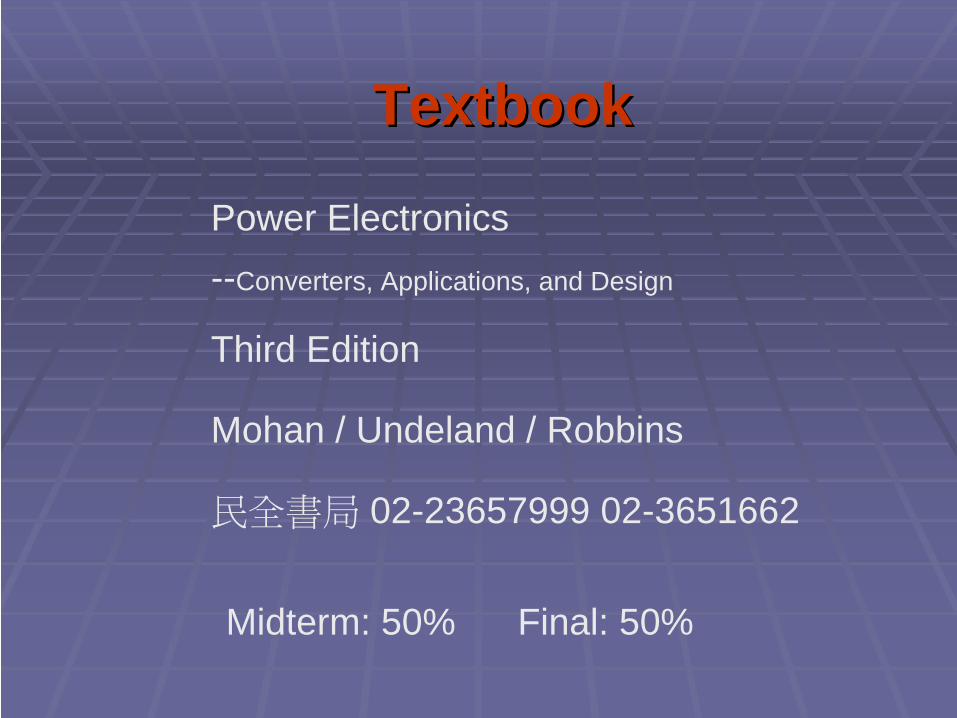
OutlinesOutlinesPower Electronic Systems
Overview of Power Semiconductor Switches
Switch-Mode DC/DC Converters
Switch-Mode DC/AC Inverters
Resonant Converters
Switching DC Power Supplies
Power Conditioners and Uninterruptible Power Supplies
Practical Converter Design Considerations

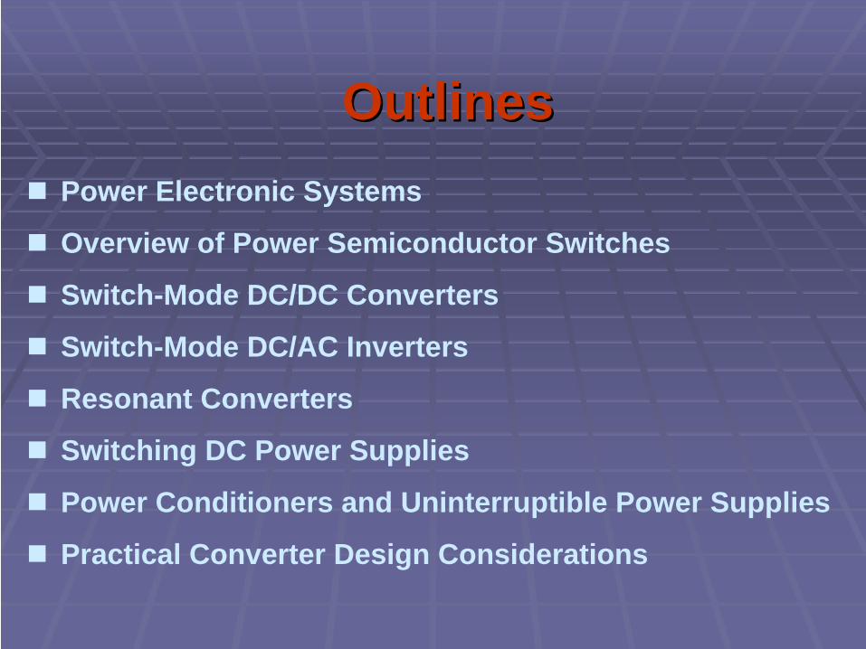
Chapter 1Chapter 1 Power Electronic SystemsPower Electronic Systems
Power Electronic SystemsPower Electronic Systems
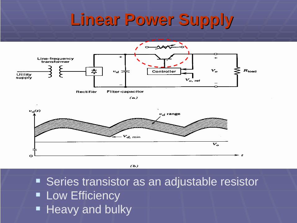
Linear Power SupplyLinear Power Supply
Series transistor as an adjustable resistorLow EfficiencyHeavy and bulky
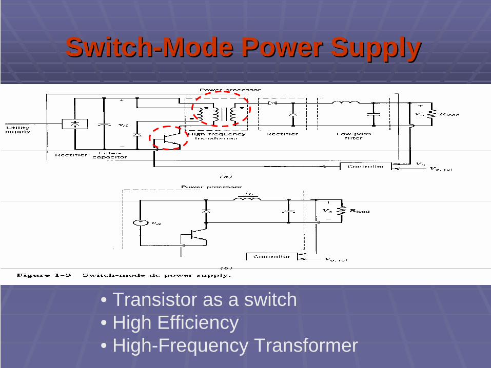
SwitchSwitch--Mode Power SupplyMode Power Supply
• Transistor as a switch• High Efficiency• High-Frequency Transformer
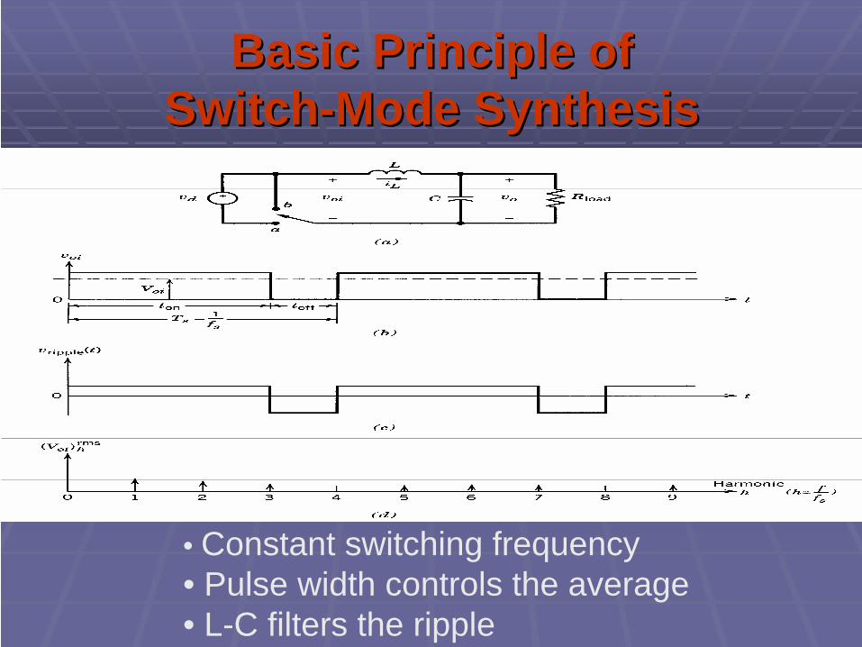
Basic Principle of Basic Principle of SwitchSwitch--Mode SynthesisMode Synthesis
• Constant switching frequency• Pulse width controls the average• L-C filters the ripple

Application Application in Adjustable Speed Drivesin Adjustable Speed Drives
• Conventional drive wastes energy across the throttling valve to adjust flow rate
• Using power electronics, motor-pump speed is adjusted efficiently to deliver the required flow rate
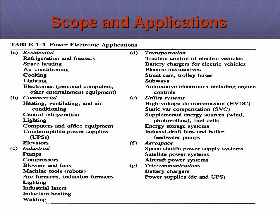
Scope and ApplicationsScope and Applications

Scope and ApplicationsScope and Applications

ac-dc converters (controlled rectifiers)
dc-dc converters (dc choppers)
dc-ac converters (inverters)
ac-ac converters (ac voltage controllers)
Classification of Power ConvertersClassification of Power Converters
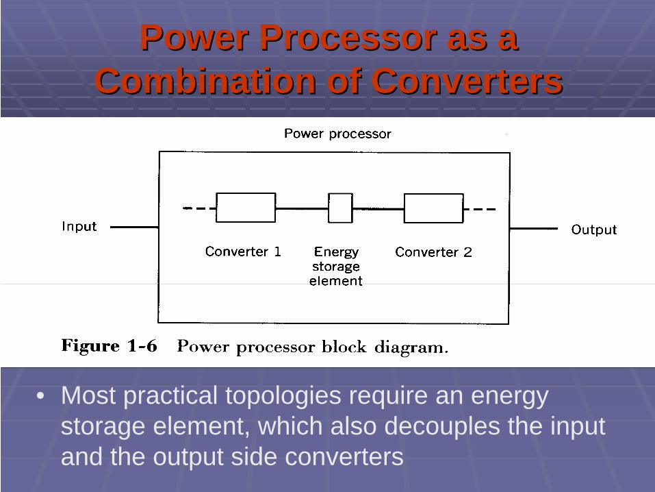
Power Processor as a Power Processor as a Combination of ConvertersCombination of Converters
• Most practical topologies require an energy storage element, which also decouples the input and the output side converters

Power Flow through ConvertersPower Flow through Converters
• Converter is a general term• An ac/dc converter is shown here• Rectifier Mode of operation when power from ac to dc• Inverter Mode of operation when power from ac to dc
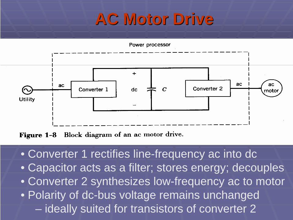
AC Motor DriveAC Motor Drive
• Converter 1 rectifies line-frequency ac into dc• Capacitor acts as a filter; stores energy; decouples• Converter 2 synthesizes low-frequency ac to motor• Polarity of dc-bus voltage remains unchanged
– ideally suited for transistors of converter 2
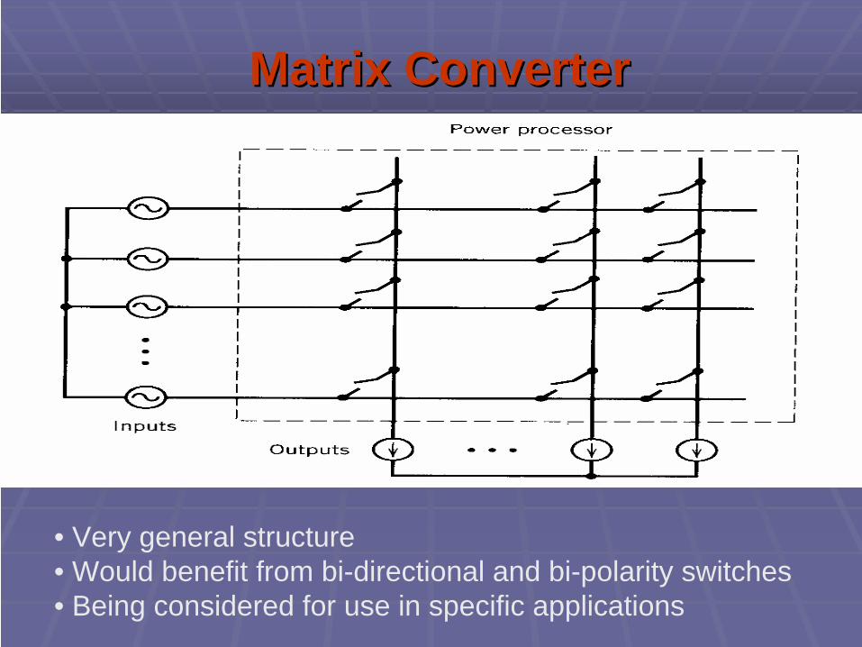
Matrix ConverterMatrix Converter
• Very general structure• Would benefit from bi-directional and bi-polarity switches• Being considered for use in specific applications

Interdisciplinary Nature of Interdisciplinary Nature of Power ElectronicsPower Electronics

Chapter 2 Overview ofChapter 2 Overview ofPower Semiconductor DevicesPower Semiconductor Devices
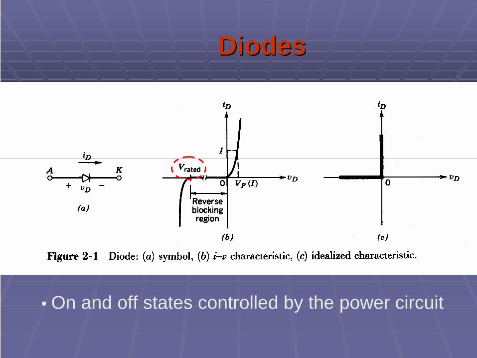
DiodesDiodes
• On and off states controlled by the power circuit
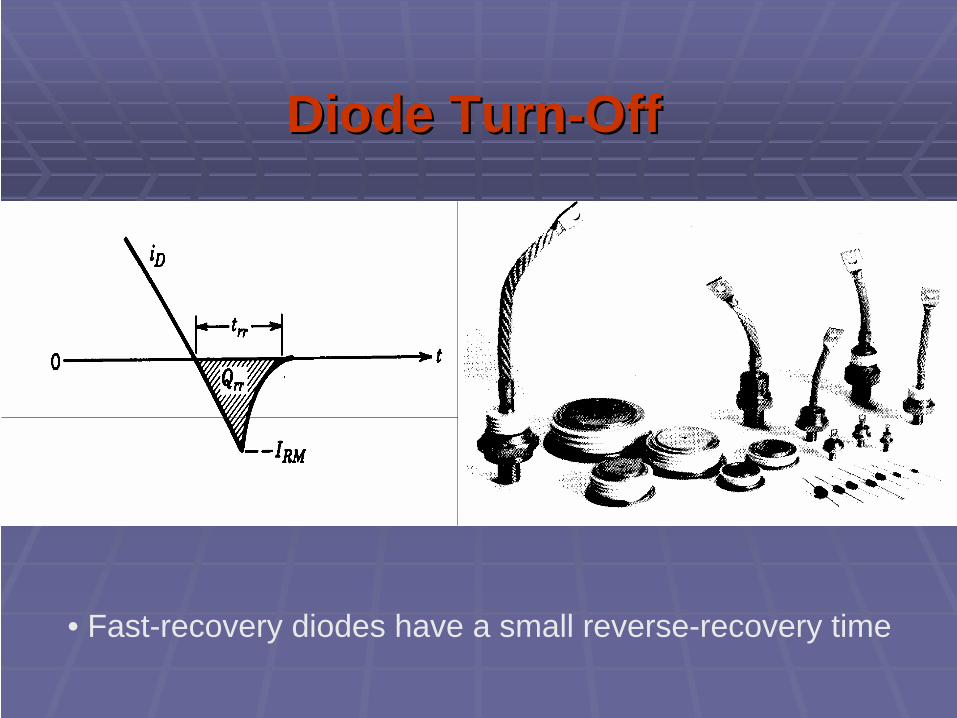
Diode TurnDiode Turn--OffOff
• Fast-recovery diodes have a small reverse-recovery time
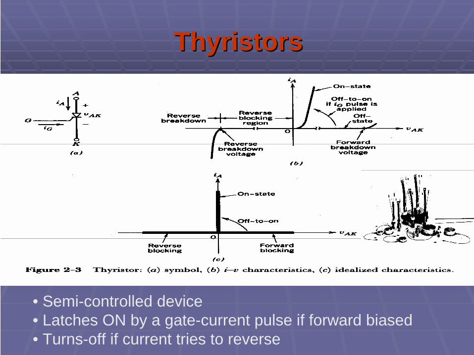
ThyristorsThyristors
• Semi-controlled device• Latches ON by a gate-current pulse if forward biased• Turns-off if current tries to reverse

Thyristor in a Simple CircuitThyristor in a Simple Circuit
• For successful turn-off, reverse voltage required for an interval greater than the turn-off interval
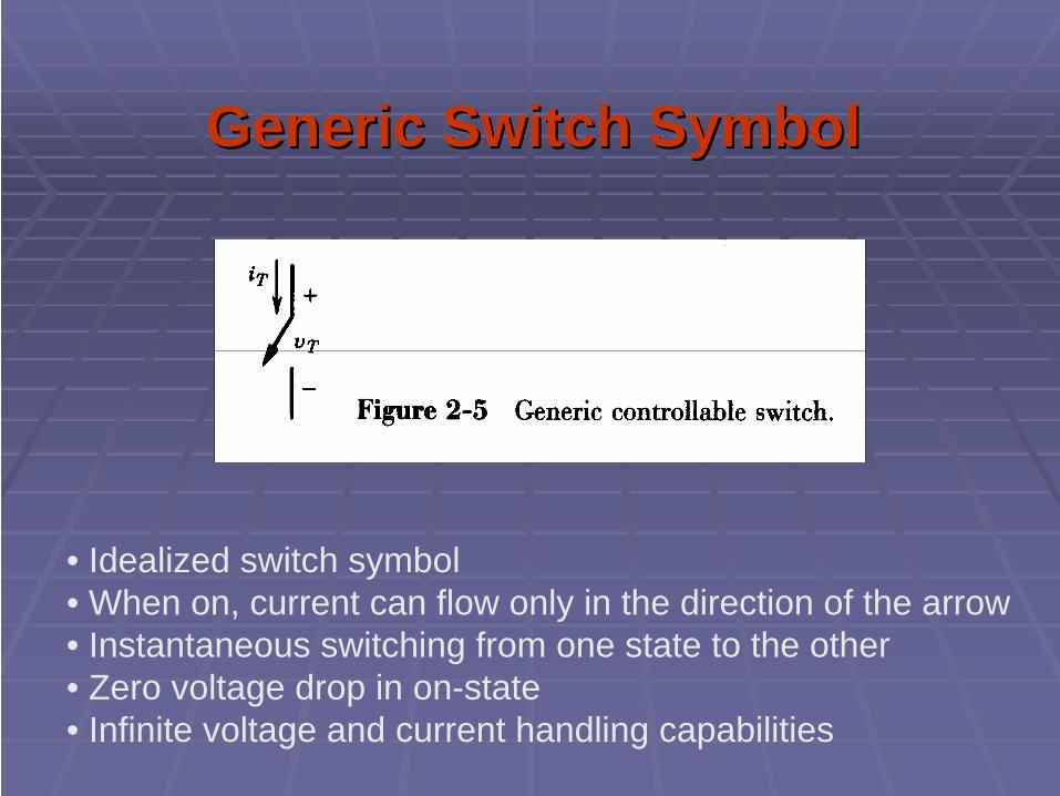
Generic Switch SymbolGeneric Switch Symbol
• Idealized switch symbol• When on, current can flow only in the direction of the arrow• Instantaneous switching from one state to the other• Zero voltage drop in on-state• Infinite voltage and current handling capabilities
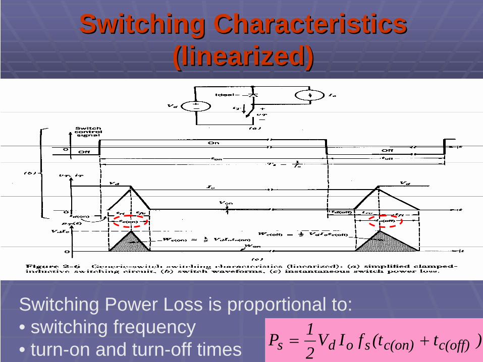
Switching Characteristics Switching Characteristics (linearized)(linearized)
Switching Power Loss is proportional to:• switching frequency• turn-on and turn-off times )t(tfIV
21P c(off)c(on)sods +=

Bipolar Junction Transistors (BJT)Bipolar Junction Transistors (BJT)
• Used commonly in the past• Now used in specific applications• Replaced by MOSFETs and IGBTs

Various Configurations of Various Configurations of BJTsBJTs

MOSFETsMOSFETs
• Easy to control by the gate• Optimal for low-voltage operation at high switching frequencies• On-state resistance a concern at higher voltage ratings

GateGate--TurnTurn--Off Thyristors (GTO)Off Thyristors (GTO)
• Slow switching speeds• Used at very high power levels• Require elaborate gate control circuitry

GTO TurnGTO Turn--OffOff
• Need a turn-off snubber
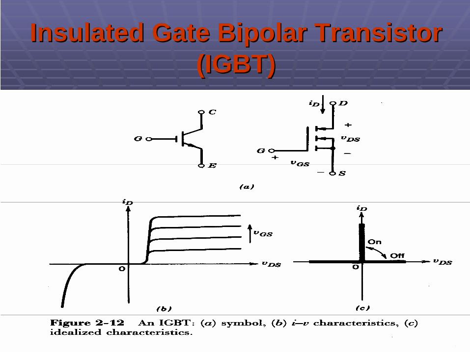
Insulated Gate Bipolar TransistorInsulated Gate Bipolar Transistor(IGBT)(IGBT)
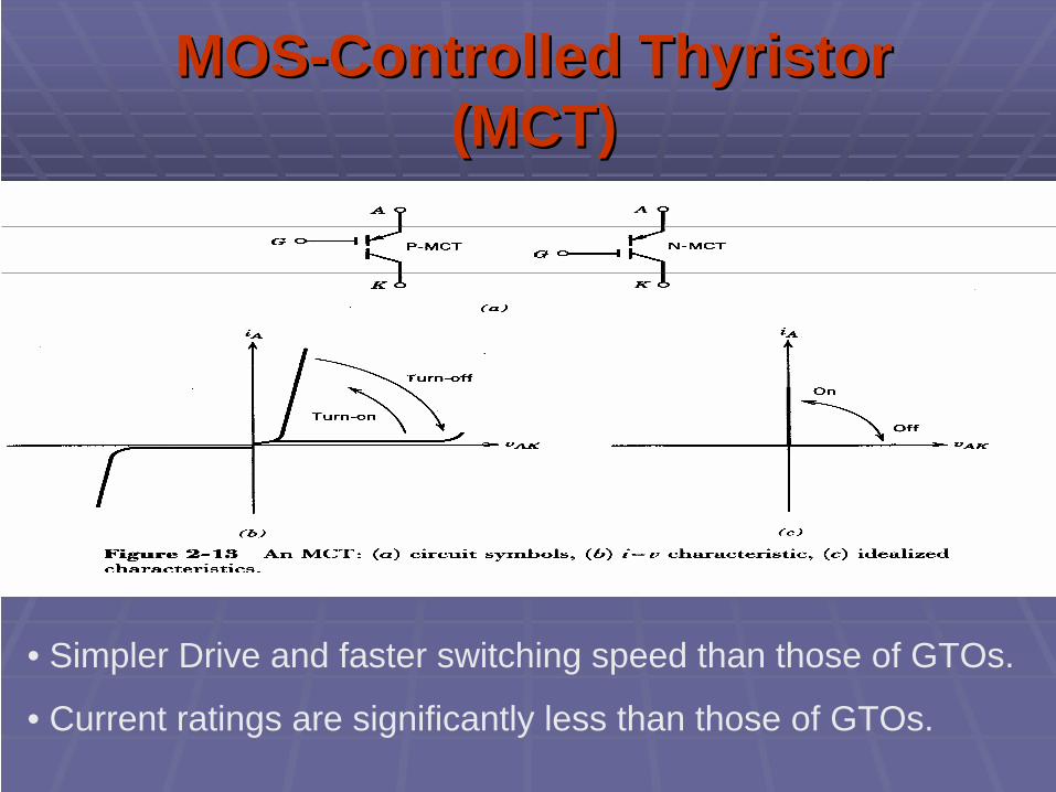
MOSMOS--Controlled Controlled ThyristorThyristor(MCT)(MCT)
• Simpler Drive and faster switching speed than those of GTOs.
• Current ratings are significantly less than those of GTOs.
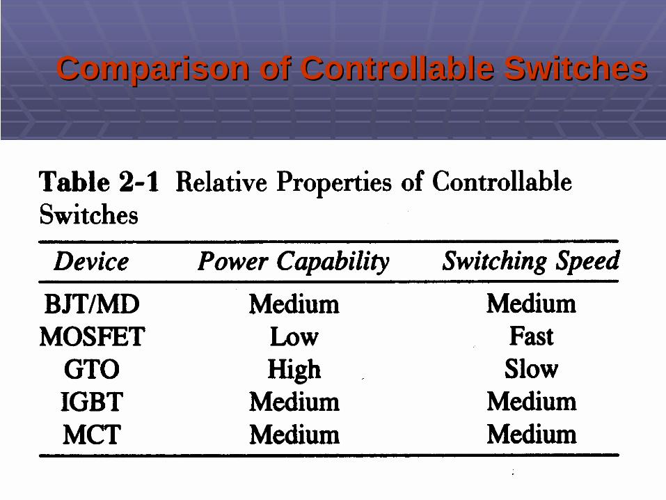
Comparison of Controllable SwitchesComparison of Controllable Switches

Summary of Device CapabilitiesSummary of Device Capabilities

Rating of Power DevicesRating of Power Devices
Chapter 3 Chapter 3
Review of Basic Electrical and Review of Basic Electrical and Magnetic Circuit ConceptsMagnetic Circuit Concepts
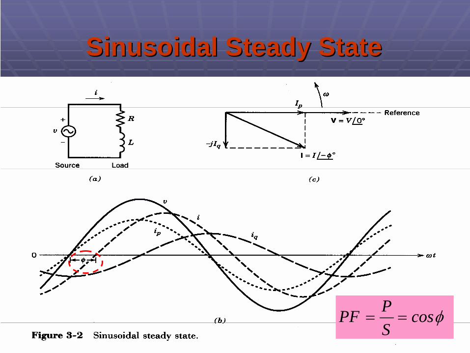
Sinusoidal Steady StateSinusoidal Steady State
φcosSPPF ==
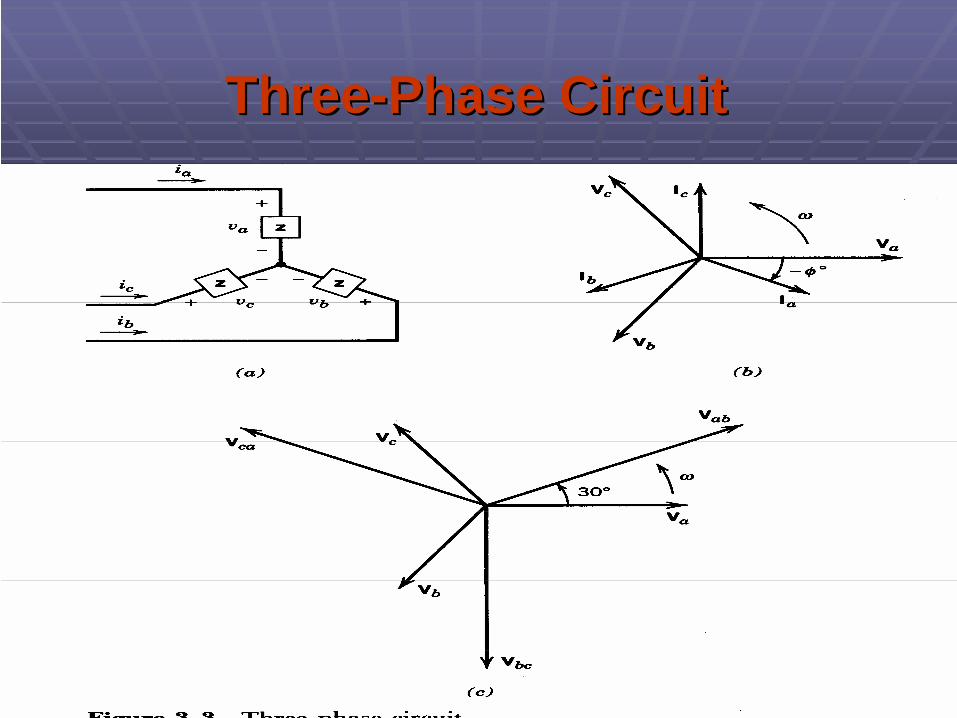
ThreeThree--Phase CircuitPhase Circuit
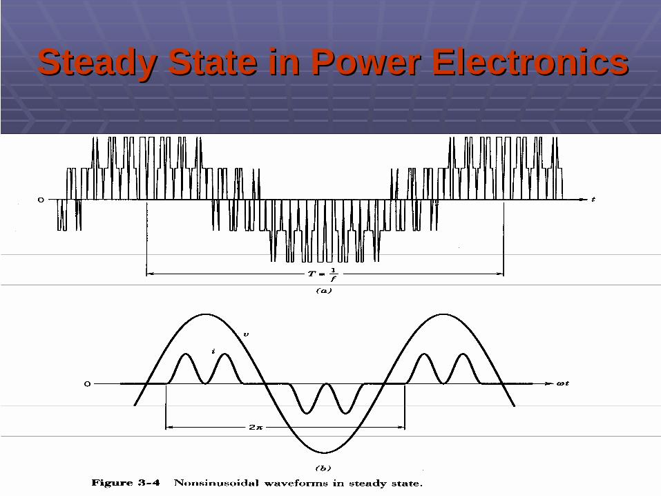
Steady State in Power ElectronicsSteady State in Power Electronics
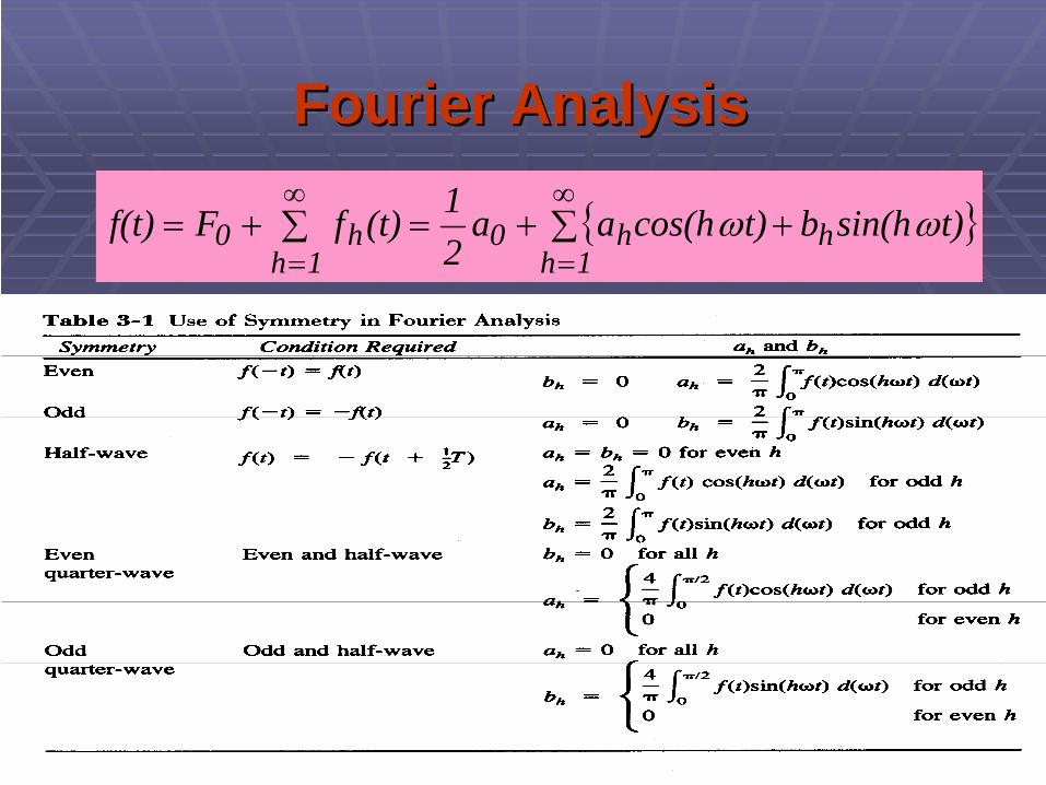
Fourier AnalysisFourier Analysis
{ }∑ +∑ +=+=∞
=
∞
= 1hhh
1h0h0 t)sin(hbt)cos(haa
21(t)fFf(t) ωω

Distortion in the Input CurrentDistortion in the Input Current
• Voltage is assumed to be sinusoidal
• Subscript “1” refers to the fundamental
• The angle is between the voltage and the current fundamental
DPFTHD1
1DPFIIcos
II
SPPF
2is
s11
s
s1
+==== φ

Phasor RepresentationPhasor Representation

Response of L and CResponse of L and C
dtdiLv L
L =dt
dvCi cc =

Inductor Voltage and Current Inductor Voltage and Current in Steady Statein Steady State
• Volt-seconds over T equal zero.
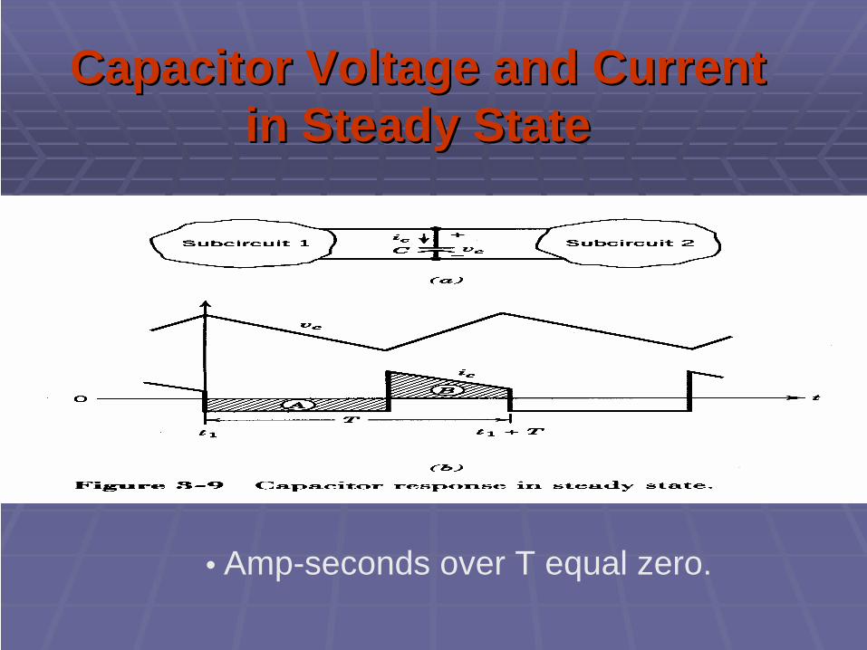
Capacitor Voltage and CurrentCapacitor Voltage and Current in Steady Statein Steady State
• Amp-seconds over T equal zero.
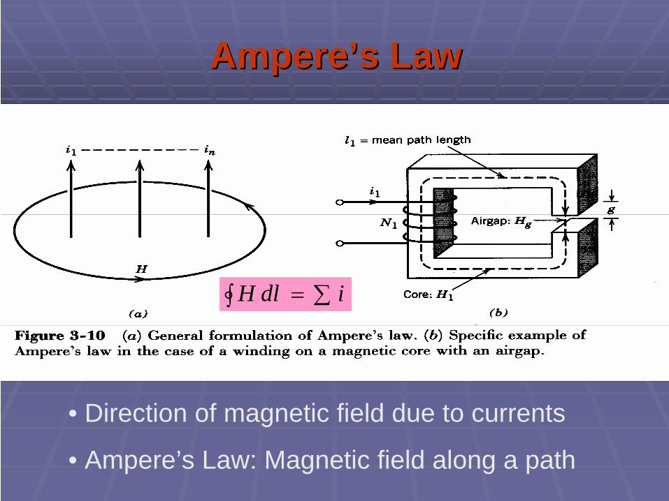
AmpereAmpere’’s Laws Law
• Direction of magnetic field due to currents
• Ampere’s Law: Magnetic field along a path
∑=∫ idlH
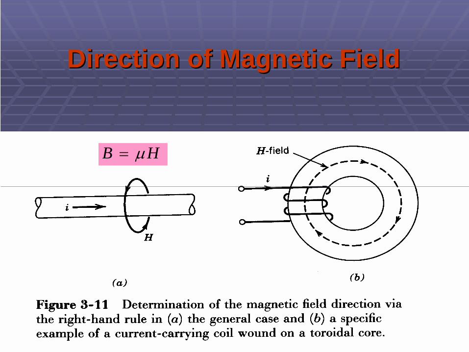
Direction of Magnetic FieldDirection of Magnetic Field
HB μ=

BB--H Relationship; SaturationH Relationship; Saturation
• Definition of permeability
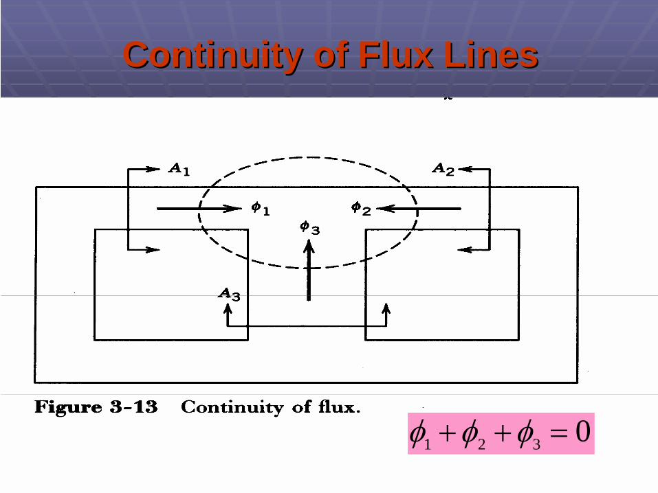
Continuity of Flux LinesContinuity of Flux Lines
1 2 3 0φ φ φ+ + =
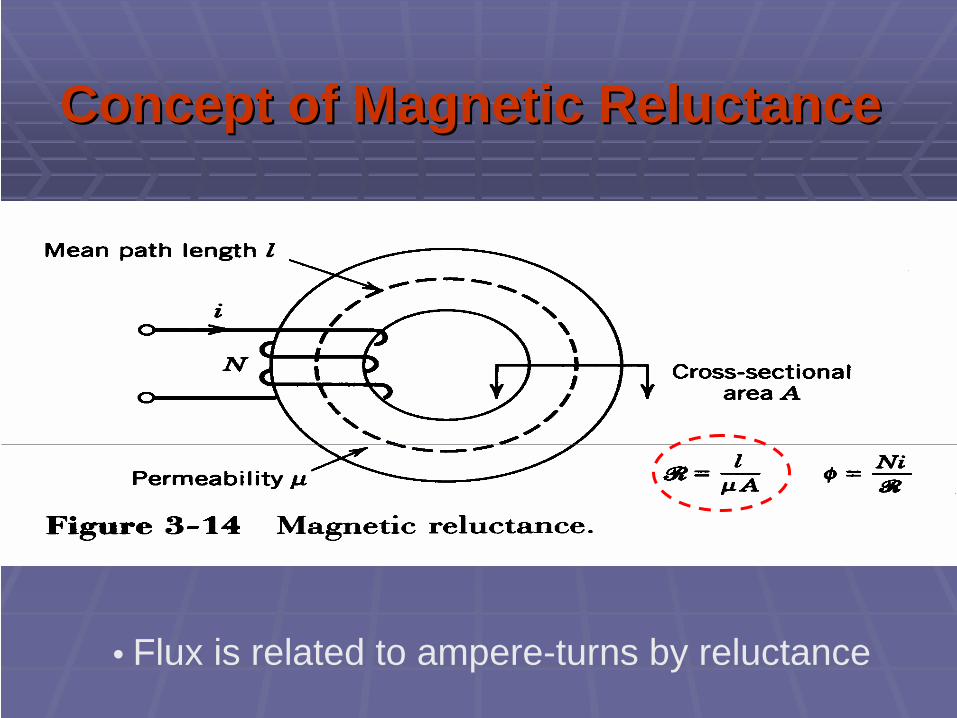
Concept of Magnetic ReluctanceConcept of Magnetic Reluctance
• Flux is related to ampere-turns by reluctance

Analogy between Electrical and Analogy between Electrical and Magnetic VariablesMagnetic Variables
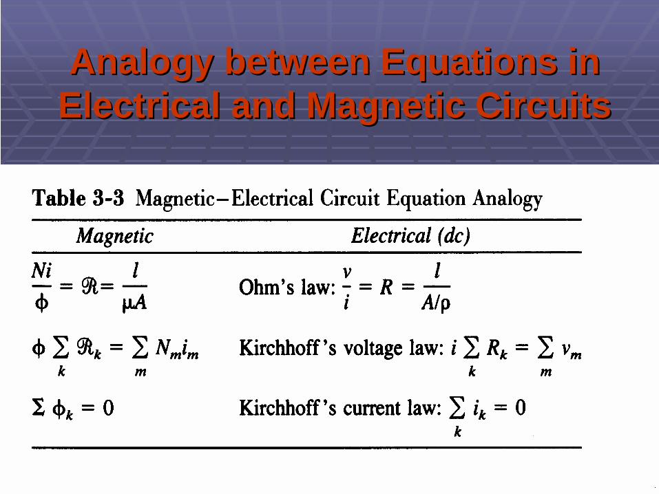
Analogy between Equations in Analogy between Equations in Electrical and Magnetic CircuitsElectrical and Magnetic Circuits
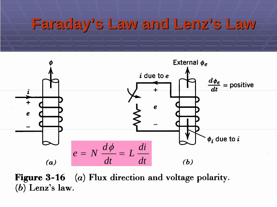
FaradayFaraday’’s Law and Lenzs Law and Lenz’’s Laws Law
dtdiL
dtdNe ==φ
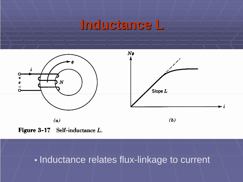
Inductance LInductance L
• Inductance relates flux-linkage to current
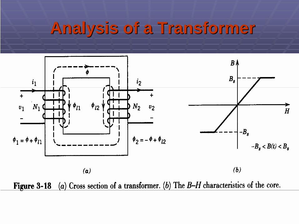
Analysis of a TransformerAnalysis of a Transformer
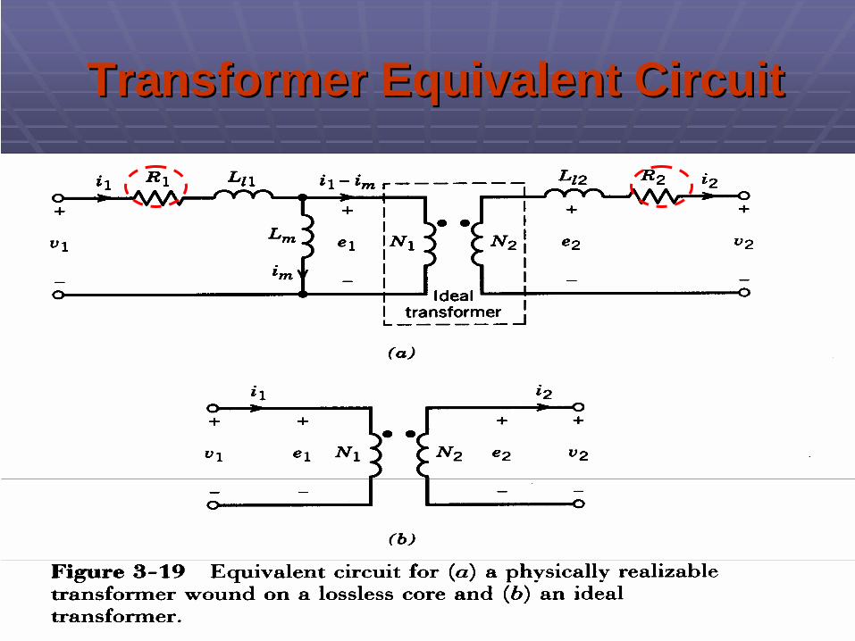
Transformer Equivalent CircuitTransformer Equivalent Circuit
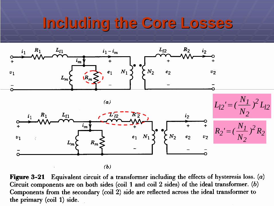
Including the Core LossesIncluding the Core Losses
l22
2
1l2 L)
NN('L =
22
2
12 R)
NN('R =
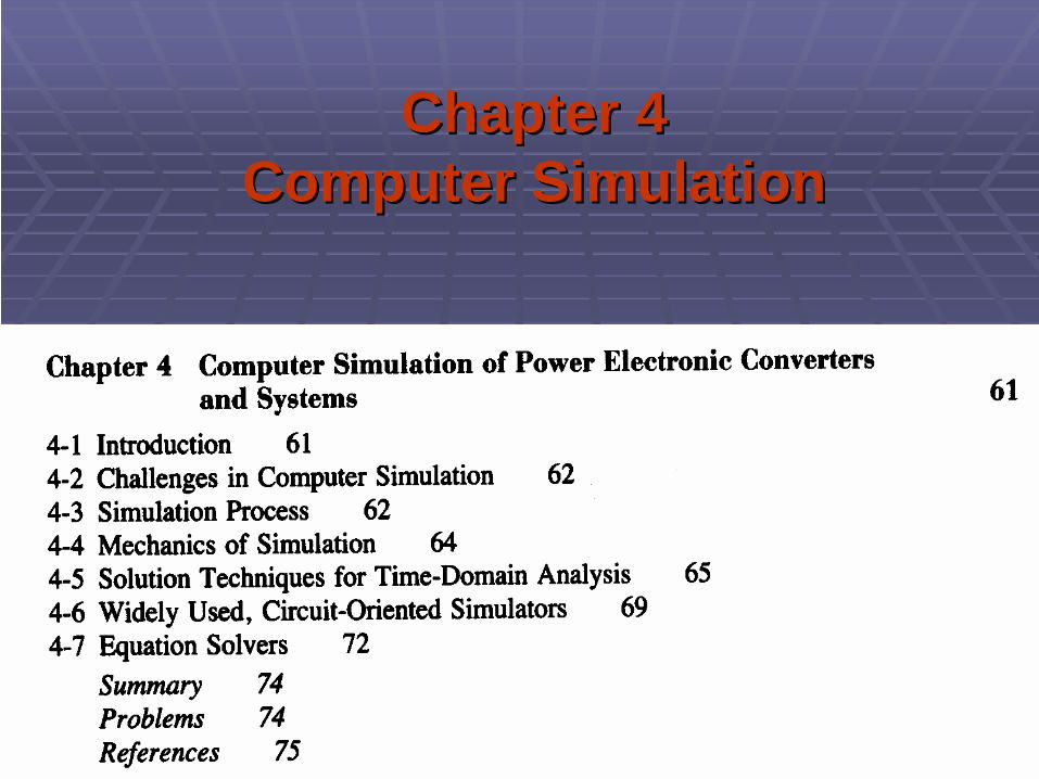
Chapter 4 Chapter 4 Computer SimulationComputer Simulation

System to be SimulatedSystem to be Simulated
• Challenges in modeling power electronic systems

LargeLarge--Signal System SimulationSignal System Simulation
• Simplest component models
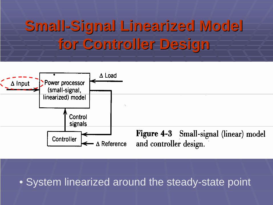
SmallSmall--Signal Signal LinearizedLinearized Model Model for Controller Designfor Controller Design
• System linearized around the steady-state point
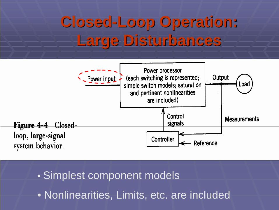
ClosedClosed--Loop Operation: Loop Operation: Large DisturbancesLarge Disturbances
• Simplest component models
• Nonlinearities, Limits, etc. are included
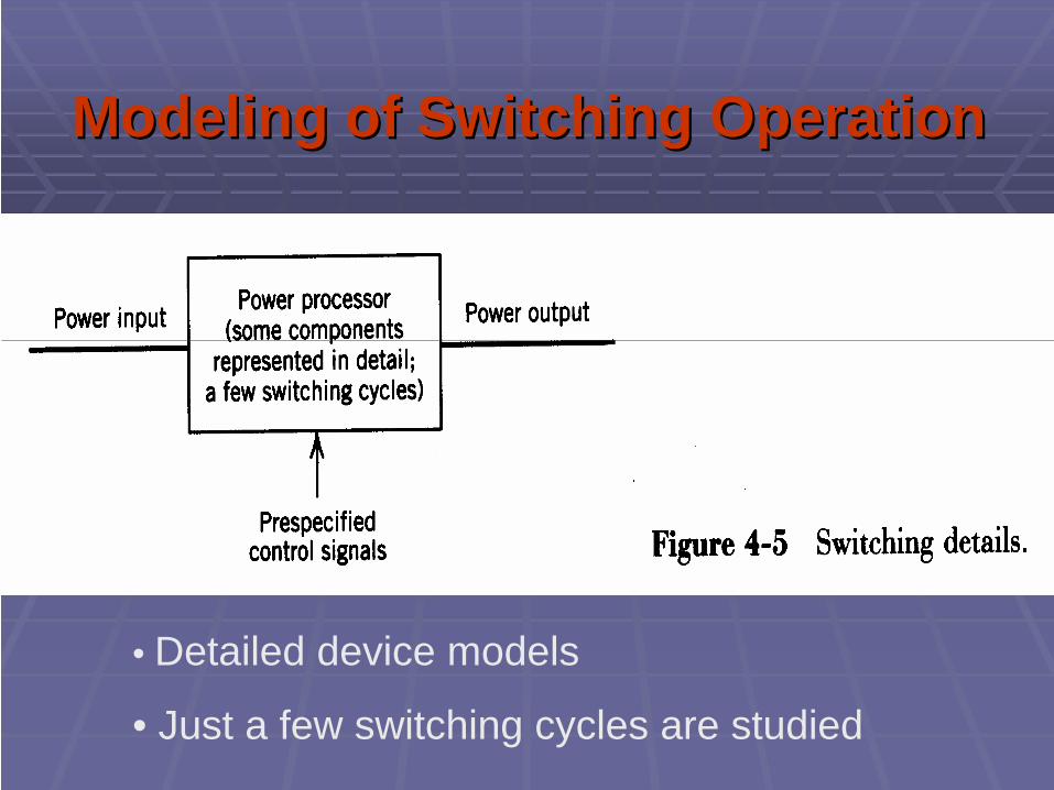
Modeling of Switching OperationModeling of Switching Operation
• Detailed device models
• Just a few switching cycles are studied

Modeling of a Simple ConverterModeling of a Simple Converter
0Rv-
dtdvC-i
vvdt
diLir
ccL
oicL
LL
=
=++
oic
LL
c
L
v0L1
vi
CR1-
C1
L1-
Lr-
dtdvdt
di
⎥⎥
⎦
⎤
⎢⎢
⎣
⎡+⎥
⎦
⎤⎢⎣
⎡
⎥⎥⎥
⎦
⎤
⎢⎢⎢
⎣
⎡
=⎥⎥⎥
⎦
⎤
⎢⎢⎢
⎣
⎡

Modeling using PSpiceModeling using PSpice
• Schematic approach is far superior

PSpicePSpice--based Simulationbased Simulation
• Simulation results
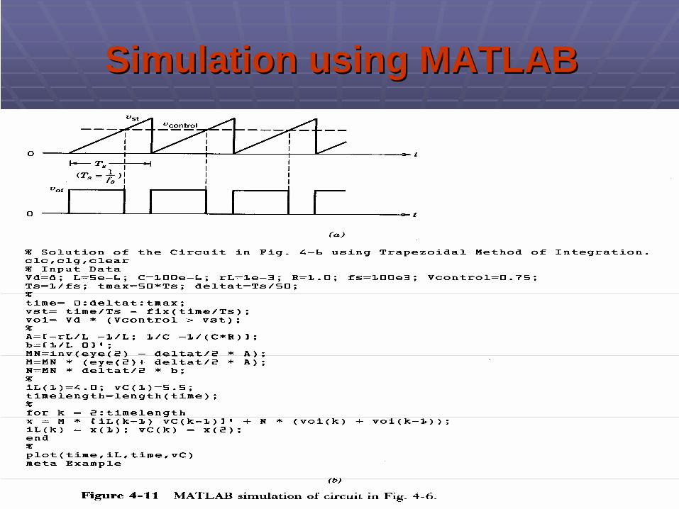
Simulation using MATLABSimulation using MATLAB

Chapter 5Chapter 5
Diode RectifiersDiode Rectifiers

Diode Rectifier Block DiagramDiode Rectifier Block Diagram
• Uncontrolled utility interface (ac to dc)
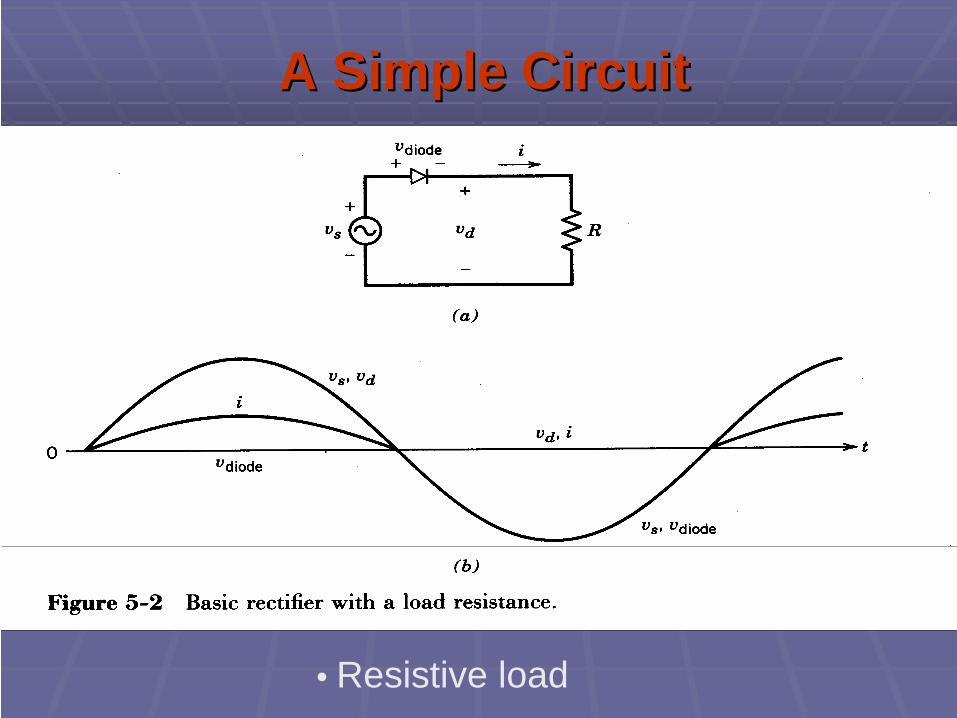
A Simple CircuitA Simple Circuit
• Resistive load
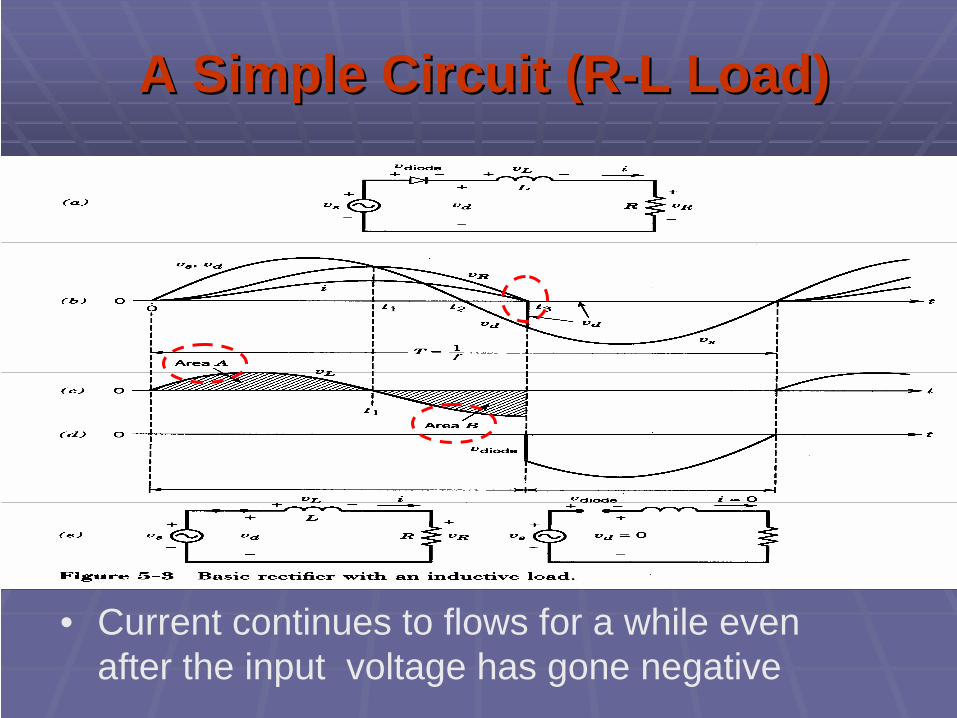
A Simple Circuit (RA Simple Circuit (R--L Load)L Load)
• Current continues to flows for a while even after the input voltage has gone negative

A Simple Circuit A Simple Circuit (Load has a dc back(Load has a dc back--emf)emf)
• Current begins to flow when the input voltage exceeds the dc back-emf
• Current continues to flows for a while even after the input voltage has gone below the dc back-emf

SingleSingle--Phase Diode Rectifier BridgePhase Diode Rectifier Bridge
• Large capacitor at the dc output for filtering and energy storage
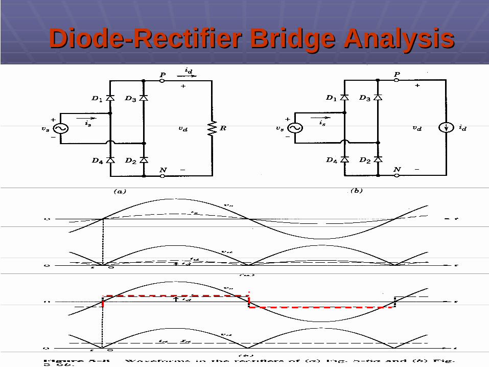
DiodeDiode--Rectifier Bridge AnalysisRectifier Bridge Analysis

DiodeDiode--Rectifier Bridge Input CurrentRectifier Bridge Input Current

Current CommutationCurrent Commutation
• Assuming inductance in this circuit to be zero

Current CommutationCurrent Commutation
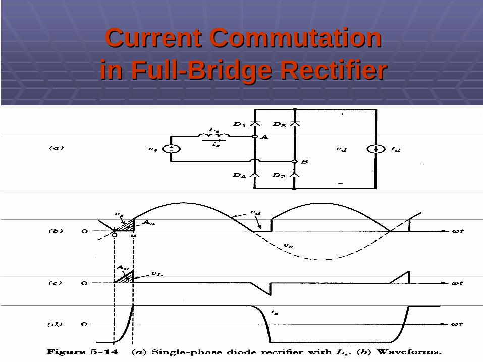
Current CommutationCurrent Commutationin Fullin Full--Bridge RectifierBridge Rectifier

Current CommutationCurrent Commutation
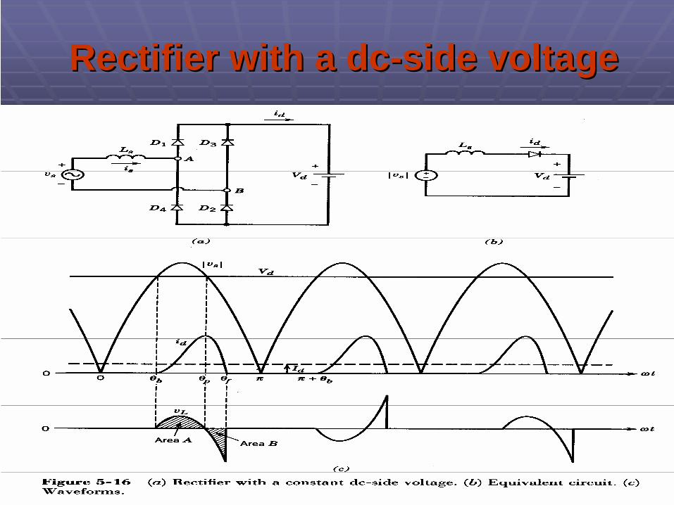
Rectifier with a dcRectifier with a dc--side voltageside voltage

DiodeDiode--Rectifier with a Capacitor FilterRectifier with a Capacitor Filter
• Power electronics load is represented by an equivalent load resistance

Diode Rectifier BridgeDiode Rectifier Bridge
• Equivalent circuit for analysis on one-half cycle basis

DiodeDiode--Bridge Rectifier: WaveformsBridge Rectifier: Waveforms
• Analysis using PSpice

• Analysis using PSpice
Input LineInput Line--Current DistortionCurrent Distortion
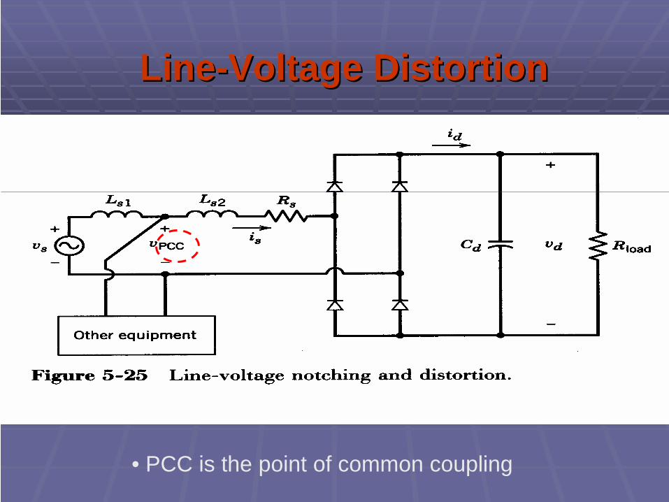
LineLine--Voltage DistortionVoltage Distortion
• PCC is the point of common coupling

• Distortion in voltage supplied to other loads
LineLine--Voltage DistortionVoltage Distortion
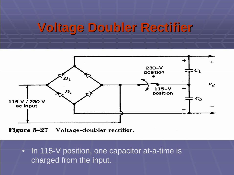
Voltage Voltage DoublerDoubler RectifierRectifier
• In 115-V position, one capacitor at-a-time is charged from the input.
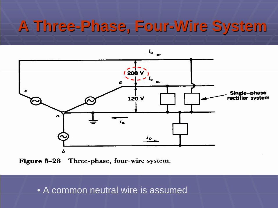
A ThreeA Three--Phase, FourPhase, Four--Wire SystemWire System
• A common neutral wire is assumed

ThreeThree--Phase, FullPhase, Full--Bridge RectifierBridge Rectifier
• Commonly used
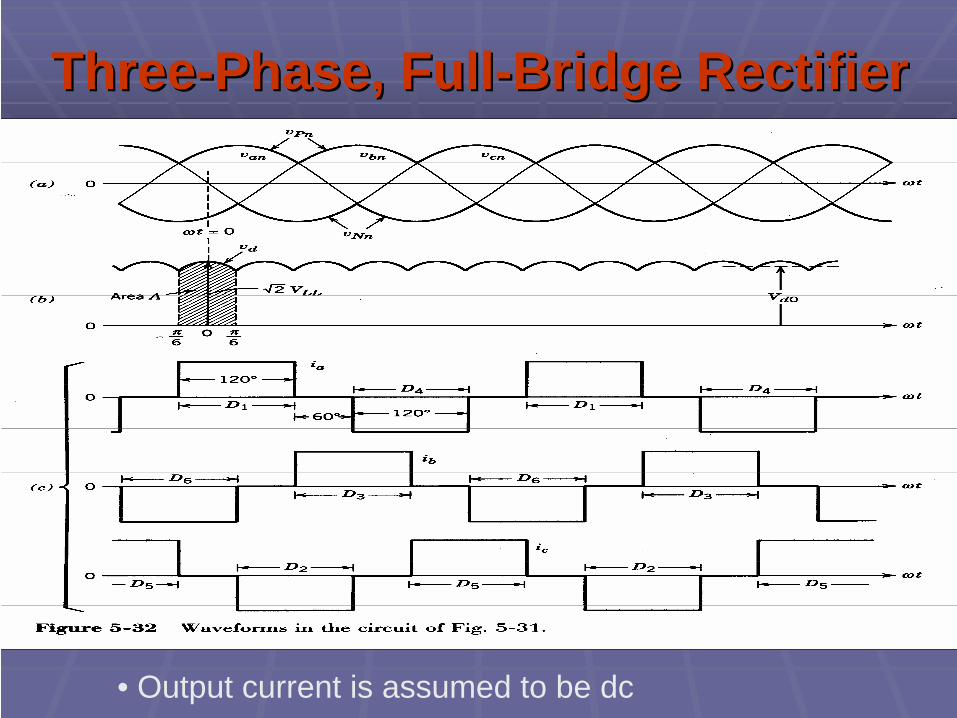
ThreeThree--Phase, FullPhase, Full--Bridge RectifierBridge Rectifier
• Output current is assumed to be dc

ThreeThree--Phase, FullPhase, Full--Bridge Rectifier: Bridge Rectifier: Input LineInput Line--CurrentCurrent
• Assuming output current to be purely dc and zero ac-side inductance
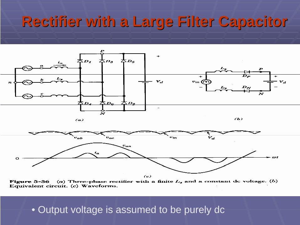
Rectifier with a Large Filter CapacitorRectifier with a Large Filter Capacitor
• Output voltage is assumed to be purely dc

Chapter 6Chapter 6Thyristor ConvertersThyristor Converters
• Controlled conversion of ac into dc
Chapter 6Chapter 6Thyristor ConvertersThyristor Converters
• Controlled conversion of ac into dc
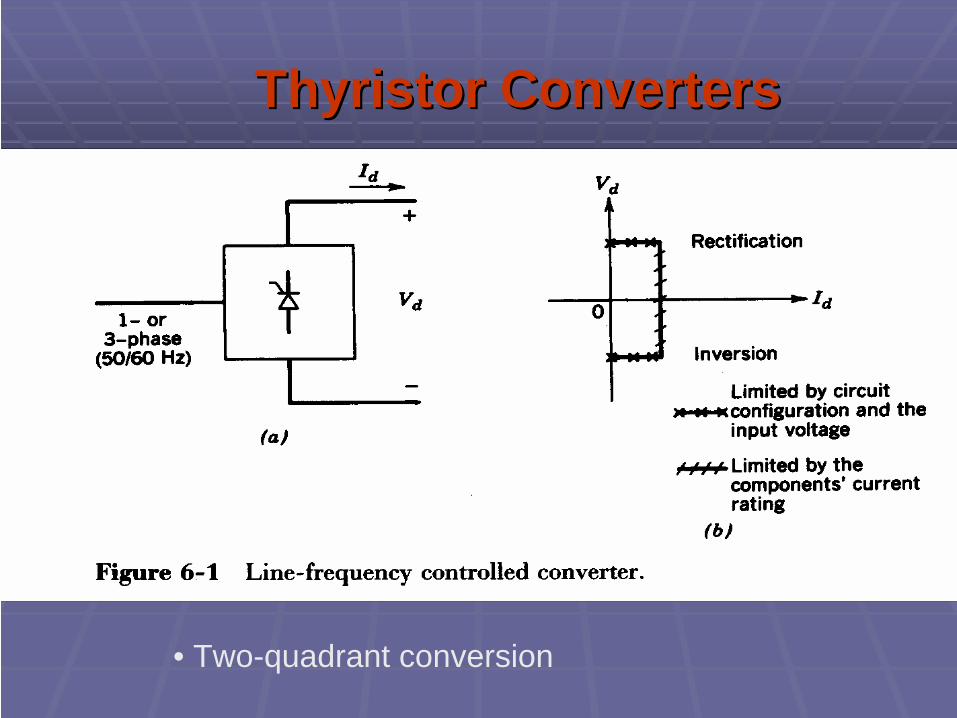
Thyristor ConvertersThyristor Converters
• Two-quadrant conversion
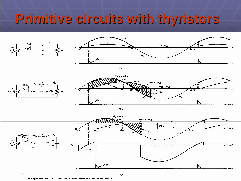
Primitive circuits with thyristorsPrimitive circuits with thyristors

Thyristor TriggeringThyristor Triggering
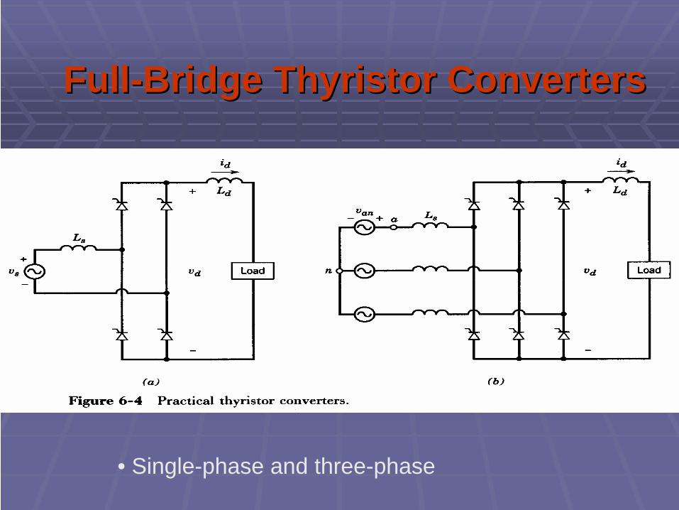
FullFull--Bridge Thyristor ConvertersBridge Thyristor Converters
• Single-phase and three-phase
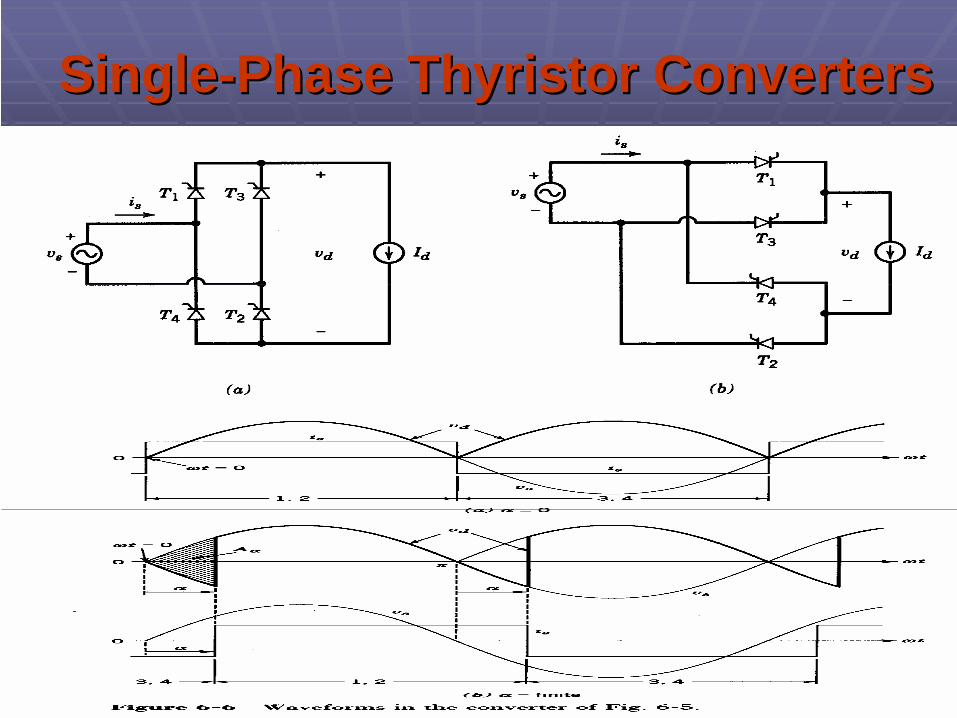
SingleSingle--Phase Thyristor ConvertersPhase Thyristor Converters

Average DC Output VoltageAverage DC Output Voltage
• Assuming zero ac-side inductance
...)]-tsin[3(II2)-tsin(I2t)(i s1s3s1s +∂+∂= ωωω
dds1 0.9II22I ==π
∂=⇒ 0.9cosP
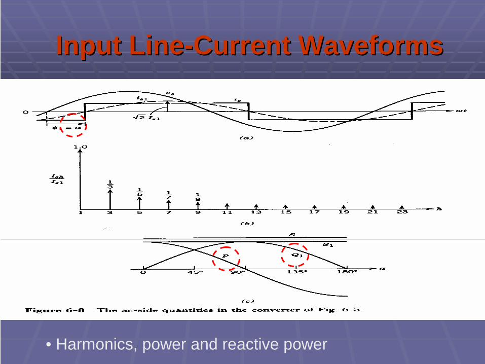
Input LineInput Line--Current WaveformsCurrent Waveforms
• Harmonics, power and reactive power
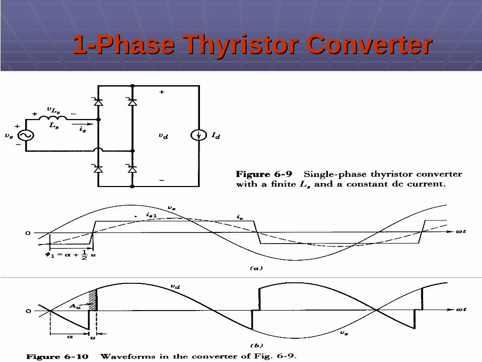
11--Phase Thyristor ConverterPhase Thyristor Converter

Thyristor ConverterThyristor Converter
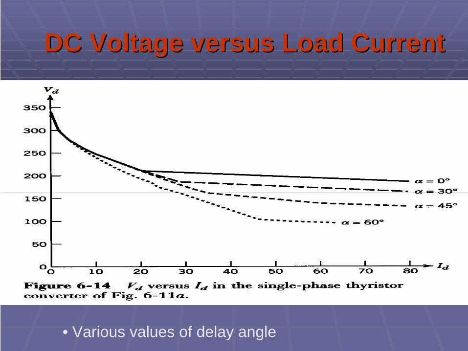
DC Voltage versus Load CurrentDC Voltage versus Load Current
• Various values of delay angle

Thyristor Converters:Thyristor Converters:Inverter ModeInverter Mode
• Assuming the ac-side inductance to be zero
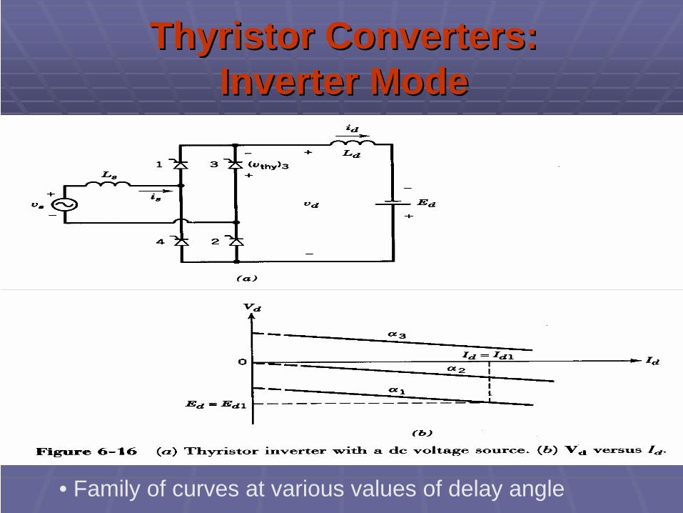
Thyristor Converters:Thyristor Converters:Inverter ModeInverter Mode
• Family of curves at various values of delay angle
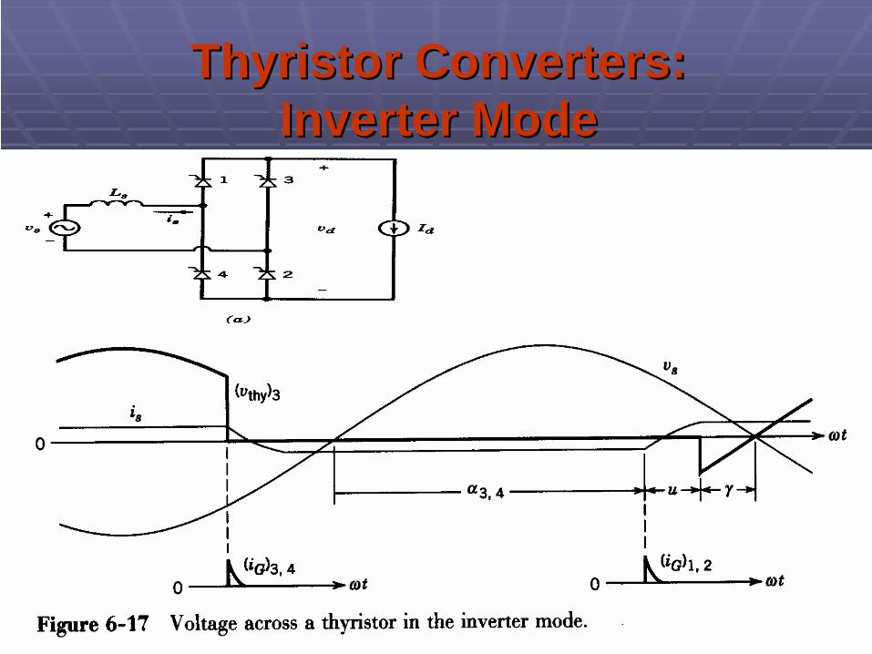
Thyristor Converters:Thyristor Converters:Inverter ModeInverter Mode

Thyristor Converters:Thyristor Converters:Inverter ModeInverter Mode
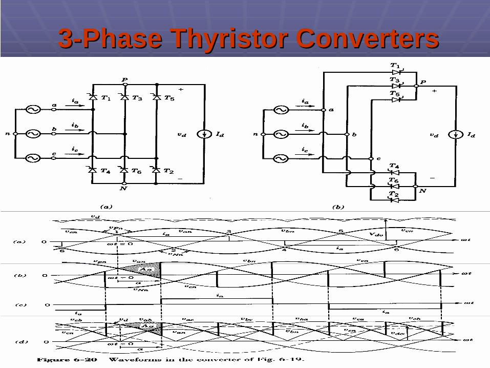
33--Phase Thyristor ConvertersPhase Thyristor Converters


Chapter 7Chapter 7DCDC--DC SwitchDC Switch--Mode ConvertersMode Converters
• dc-dc converters for switch-mode dc power supplies and dc-motor drives

Block Diagram of DCBlock Diagram of DC--DC ConvertersDC Converters
• Functional block diagram

Stepping Down a DC VoltageStepping Down a DC Voltage
• A simple approach that shows the evolution
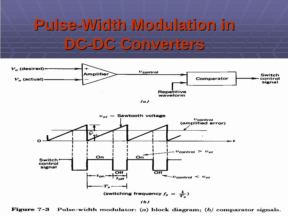
PulsePulse--Width Modulation in Width Modulation in DCDC--DC ConvertersDC Converters

StepStep--Down DCDown DC--DC ConverterDC Converter
offoonod TVTVV =− )(
1<== DT
TVV on
d
o

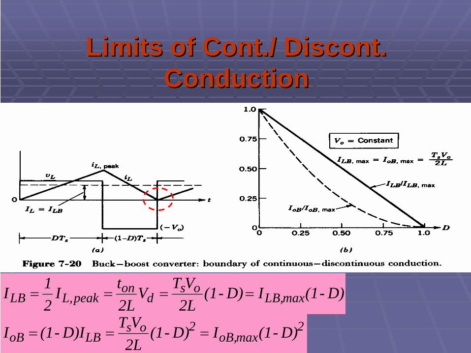
Waveforms at the boundary of Waveforms at the boundary of Cont./ Cont./ DiscontDiscont. Conduction. Conduction
• Critical current below which inductor current becomes discontinuous
D)-D(14ID)-D(12LVT)V-(V
2LtI
21I maxLB,
dsod
onpeakL,LB ====
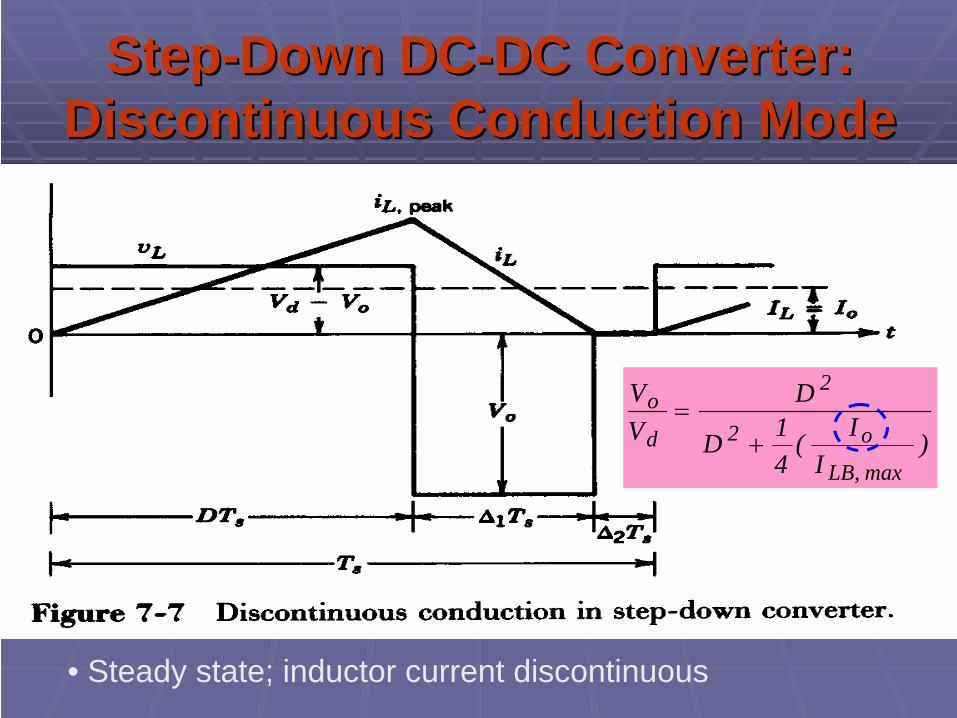
StepStep--Down DCDown DC--DC Converter: DC Converter: Discontinuous Conduction ModeDiscontinuous Conduction Mode
• Steady state; inductor current discontinuous
)I
I(41D
DVV
maxLB,
o2
2
d
o
+=

Limits of Cont./ Limits of Cont./ DiscontDiscont. . ConductionConduction
DCM:)
II(
41D
DVV
maxLB,
o2
2
d
o
+=
CCM:DVV
d
o =
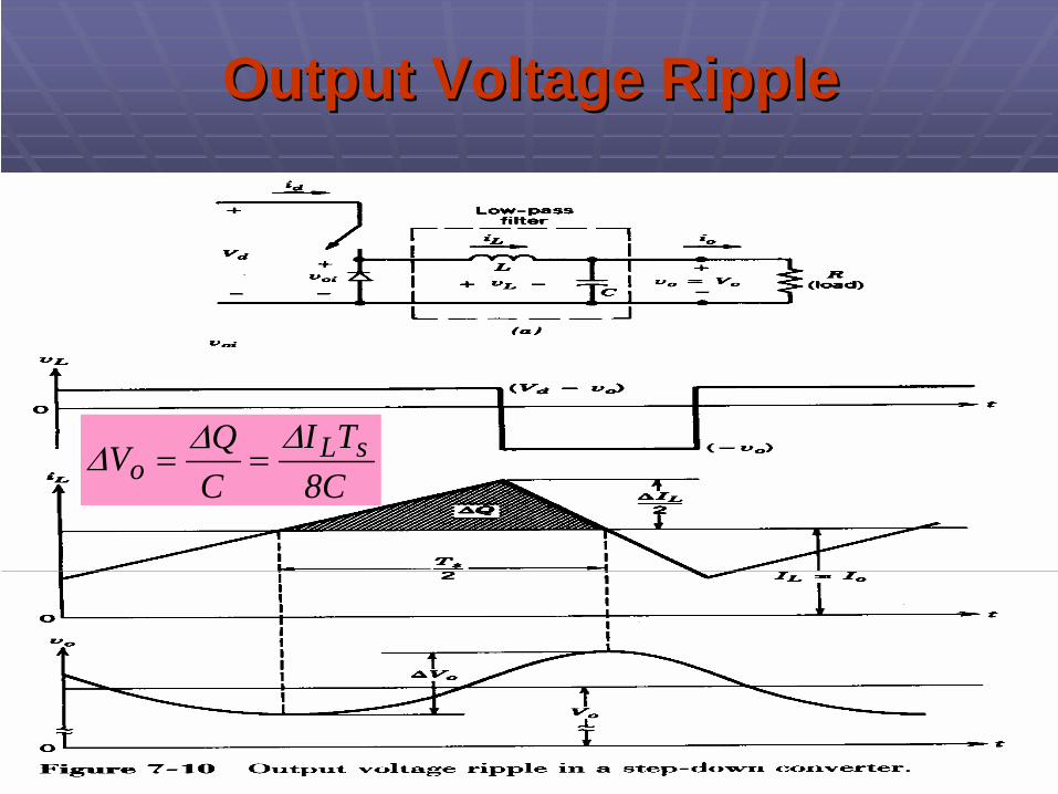
Output Voltage RippleOutput Voltage Ripple
8CTI
CQV sL
oΔΔΔ ==
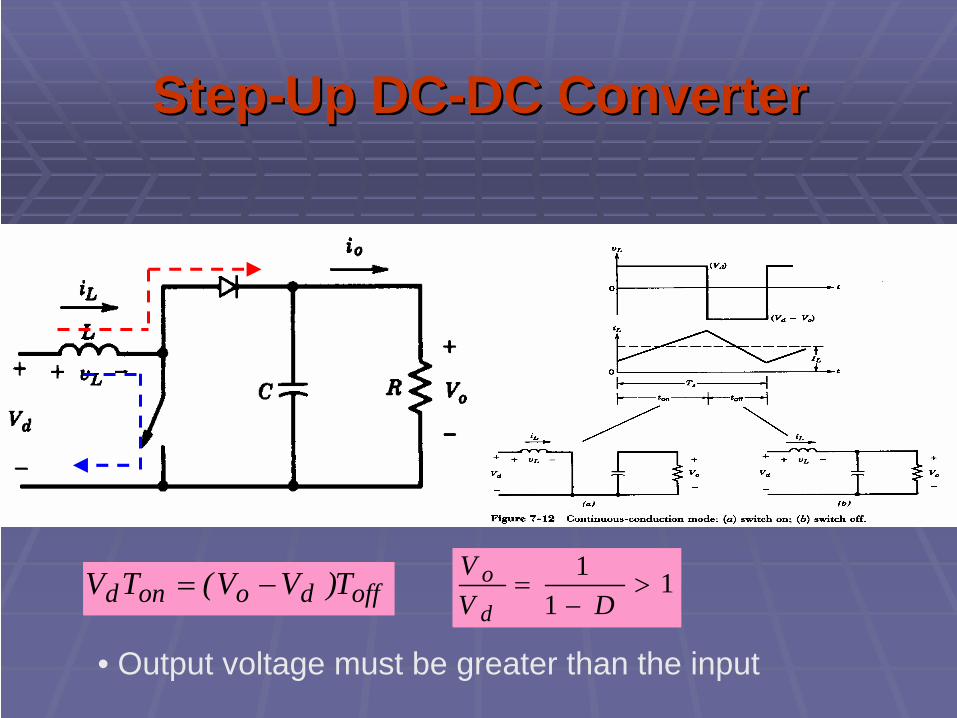
StepStep--Up DCUp DC--DC ConverterDC Converter
• Output voltage must be greater than the input
offdoond T)VV(TV −= 11
1>
−=
DVV
d
o
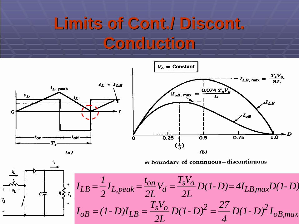
Limits of Cont./ Limits of Cont./ DiscontDiscont. . ConductionConduction
D)-D(14ID)-D(12LVTV
2LtI
21I maxLB,
osd
onpeakL,LB ====
maxoB,22os
LBoB ID)-D(14
27D)-D(12LVTD)I-(1I ===
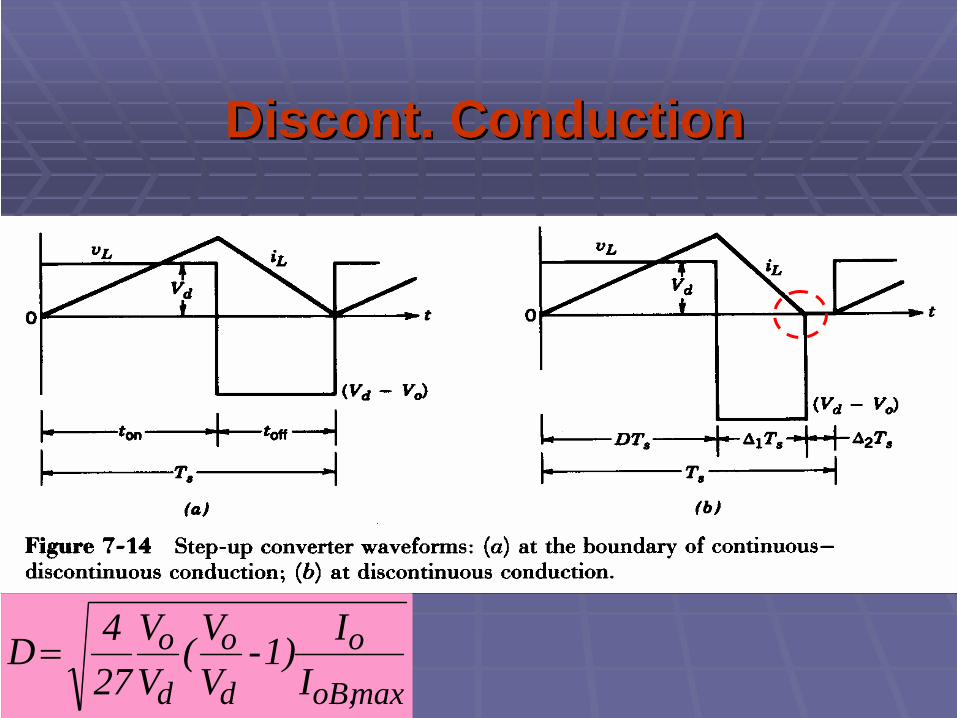
DiscontDiscont. Conduction. Conduction
maxoB,
o
d
o
d
oI
I1)-VV(
VV
274D=

Limits of Cont./ Limits of Cont./ DiscontDiscont. . ConductionConduction
DCM:I
I1)-VV(
VV
274D
maxoB,
o
d
o
d
o=CCM:DV
V
d
o−
=1
1
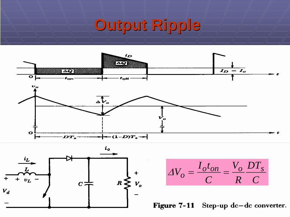
Output RippleOutput Ripple
CDT
RV
CtIV soono
o ==Δ

StepStep--Down/Up DCDown/Up DC--DC ConverterDC Converter
• The output voltage can be higher or lower than the input voltage
offoond TVTV = DD
VV
d
o−
=1
Limits of Cont./ Limits of Cont./ DiscontDiscont. . ConductionConduction
D)-(1ID)-(12LVTV
2LtI
21I maxLB,
osd
onpeakL,LB ====
2maxoB,
2osLBoB D)-(1ID)-(1
2LVTD)I-(1I ===
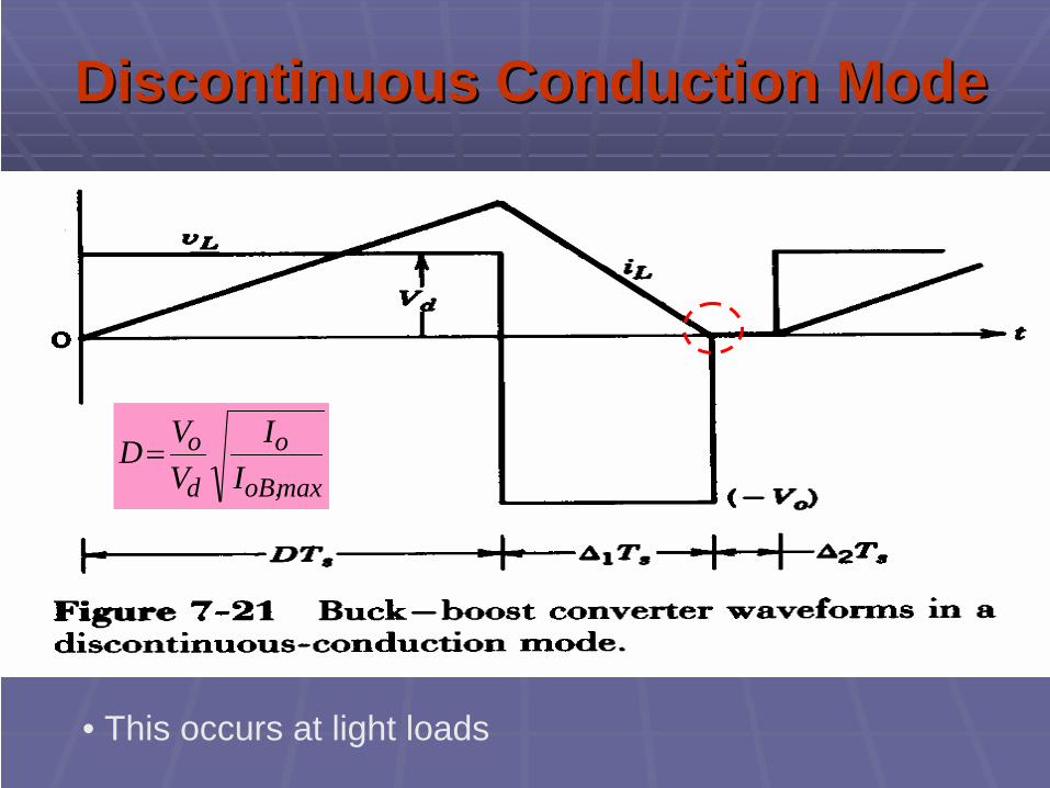
Discontinuous Conduction ModeDiscontinuous Conduction Mode
• This occurs at light loads
maxoB,
o
d
oI
IVVD=
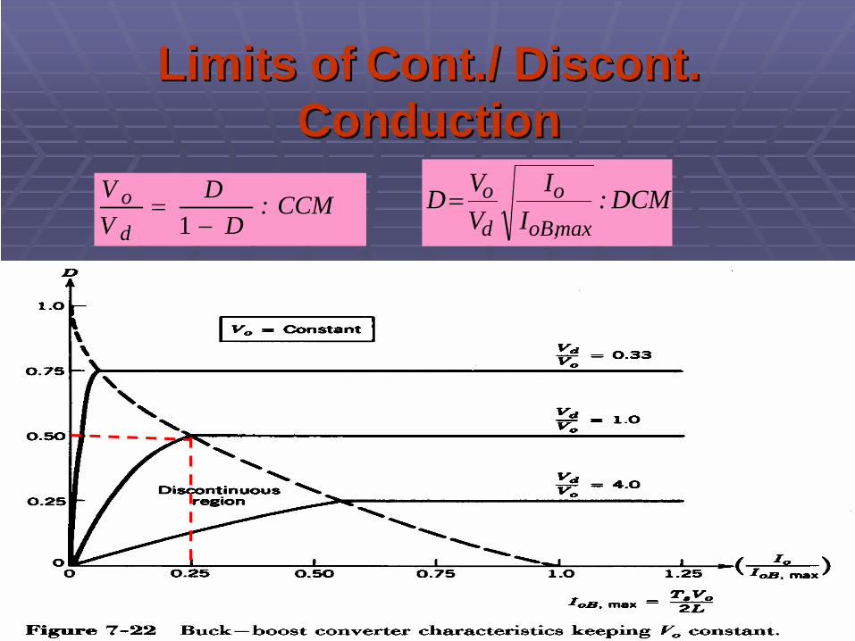
Limits ofLimits of Cont./ Cont./ DiscontDiscont. . ConductionConduction
CCM:D
DVV
d
o−
=1
DCM:I
IVVD
maxoB,
o
d
o=
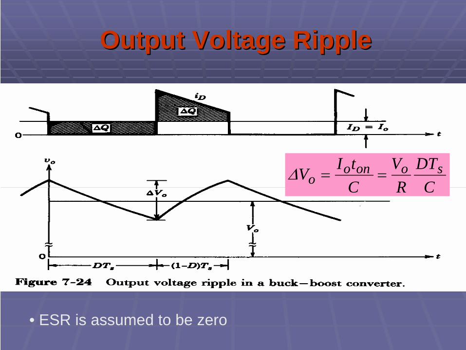
Output Voltage RippleOutput Voltage Ripple
• ESR is assumed to be zero
CDT
RV
CtIV soono
o ==Δ
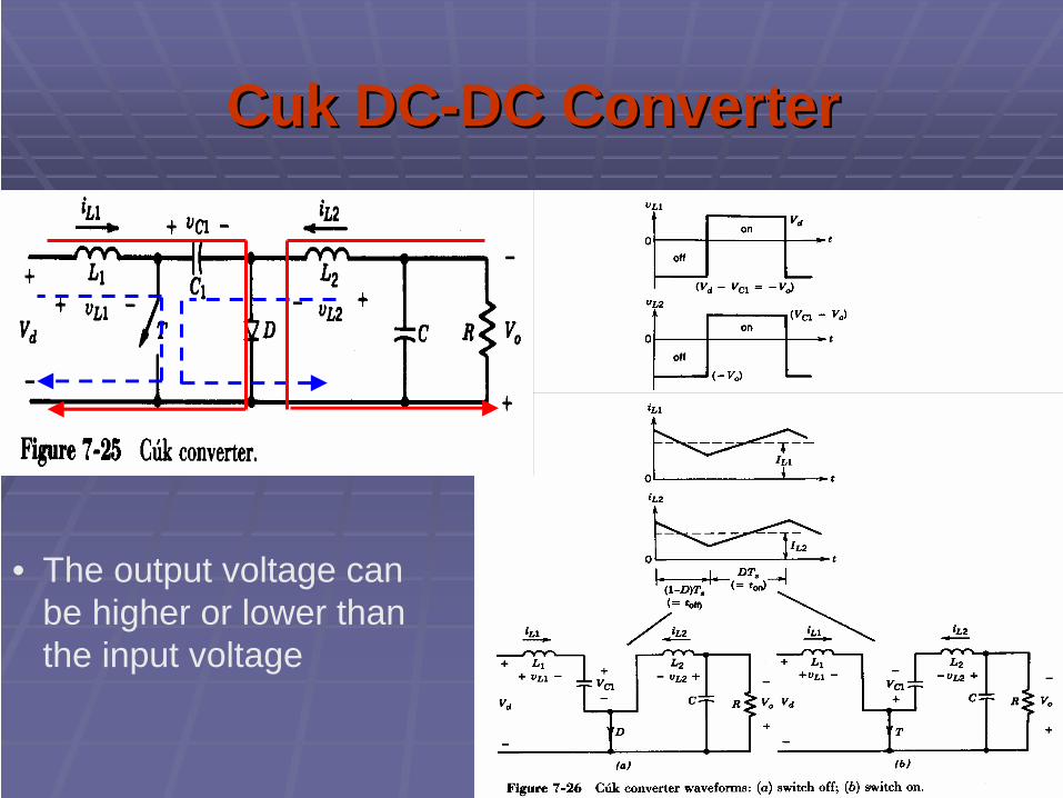
CukCuk DCDC--DC ConverterDC Converter
• The output voltage can be higher or lower than the input voltage
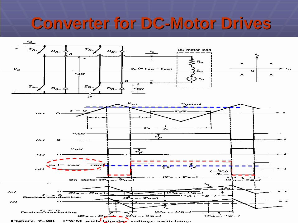
Converter for DCConverter for DC--Motor DrivesMotor Drives

Converter WaveformsConverter Waveforms

Output Ripple in Converters for Output Ripple in Converters for DCDC--Motor DrivesMotor Drives
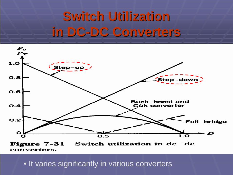
Switch UtilizationSwitch Utilizationin DCin DC--DC ConvertersDC Converters
• It varies significantly in various converters

Reversing the Power Flow Reversing the Power Flow in DCin DC--DC ConvertersDC Converters
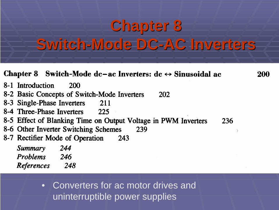
Chapter 8Chapter 8SwitchSwitch--Mode DCMode DC--AC InvertersAC Inverters
• Converters for ac motor drives and uninterruptible power supplies

SwitchSwitch--Mode DCMode DC--AC InverterAC Inverter

SwitchSwitch--Mode DCMode DC--AC InverterAC Inverter

Synthesis of a Sinusoidal OutputSynthesis of a Sinusoidal Outputby PWMby PWM
tri^
control^
aV
Vm =
1
sf f
fm =
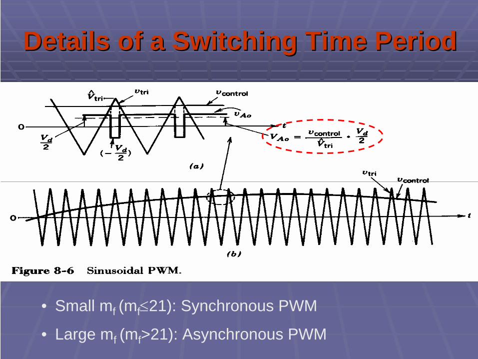
Details of a Switching Time PeriodDetails of a Switching Time Period
• Small mf (mf ≤21): Synchronous PWM
• Large mf (mf >21): Asynchronous PWM
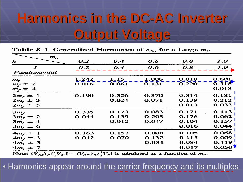
Harmonics in the DCHarmonics in the DC--AC Inverter AC Inverter Output VoltageOutput Voltage
• Harmonics appear around the carrier frequency and its multiples
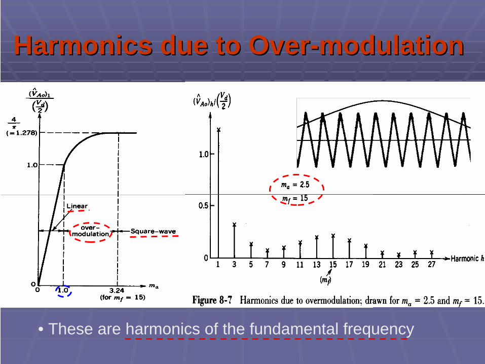
Harmonics due to OverHarmonics due to Over--modulationmodulation
• These are harmonics of the fundamental frequency
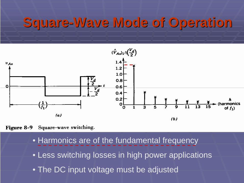
SquareSquare--Wave Mode of OperationWave Mode of Operation
• Harmonics are of the fundamental frequency
• Less switching losses in high power applications
• The DC input voltage must be adjusted
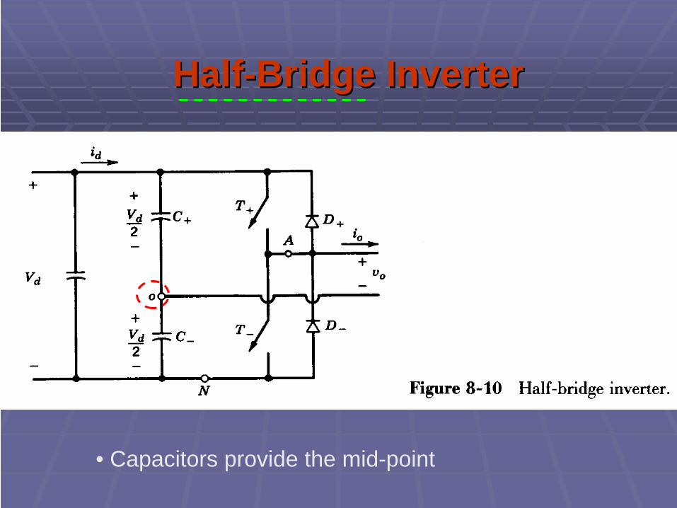
HalfHalf--Bridge InverterBridge Inverter
• Capacitors provide the mid-point
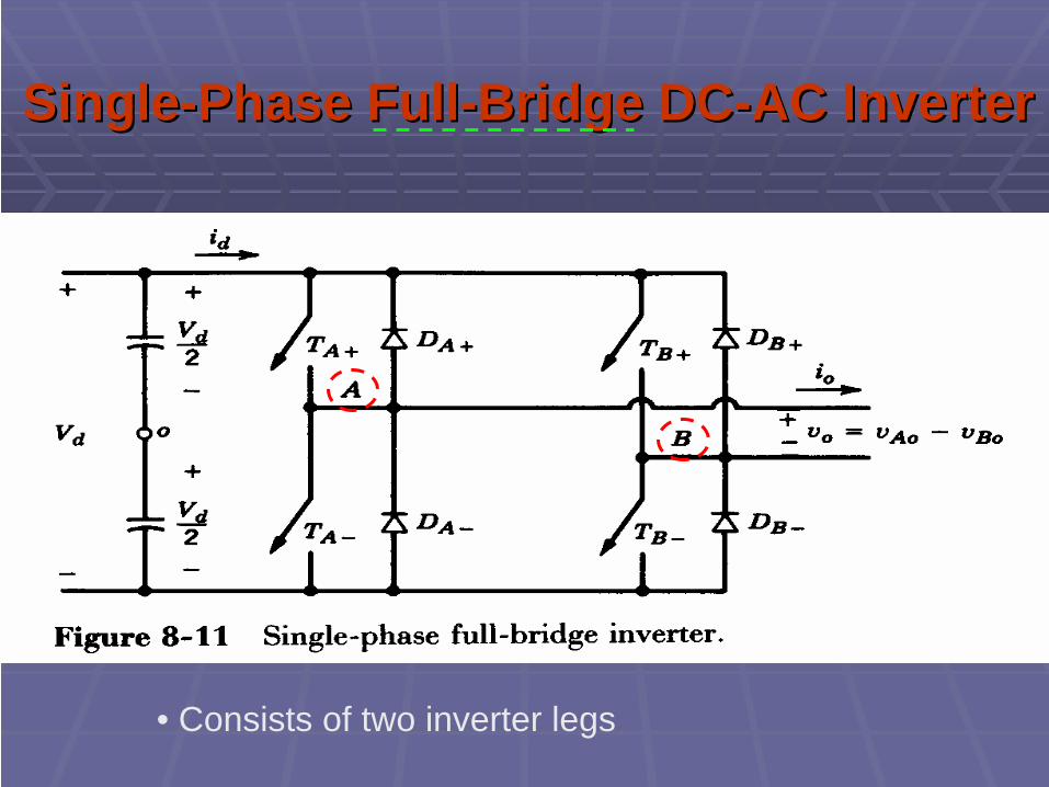
SingleSingle--Phase FullPhase Full--Bridge DCBridge DC--AC InverterAC Inverter
• Consists of two inverter legs

PWM to Synthesize Sinusoidal OutputPWM to Synthesize Sinusoidal Output
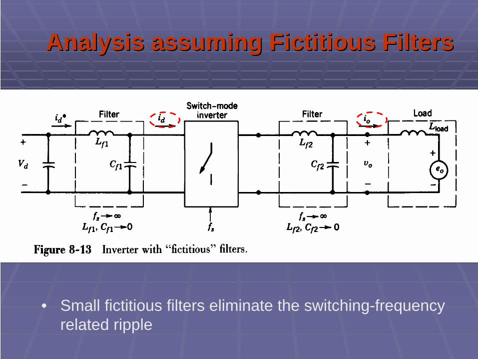
Analysis assuming Fictitious FiltersAnalysis assuming Fictitious Filters
• Small fictitious filters eliminate the switching-frequency related ripple
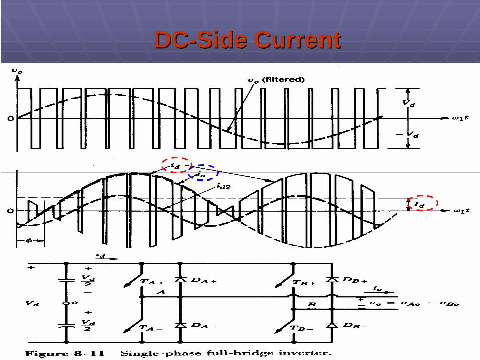
DCDC--Side CurrentSide Current
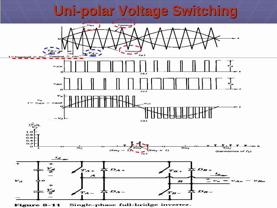
UniUni--polar Voltage Switchingpolar Voltage Switching
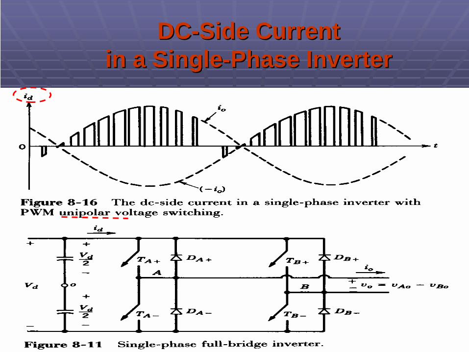
DCDC--Side CurrentSide Currentin a Singlein a Single--Phase InverterPhase Inverter
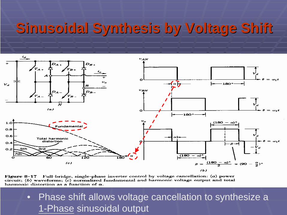
Sinusoidal Synthesis by Voltage ShiftSinusoidal Synthesis by Voltage Shift
• Phase shift allows voltage cancellation to synthesize a 1-Phase sinusoidal output

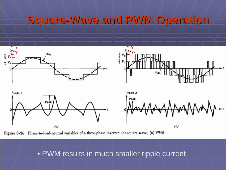
SquareSquare--Wave and PWM OperationWave and PWM Operation
• PWM results in much smaller ripple current
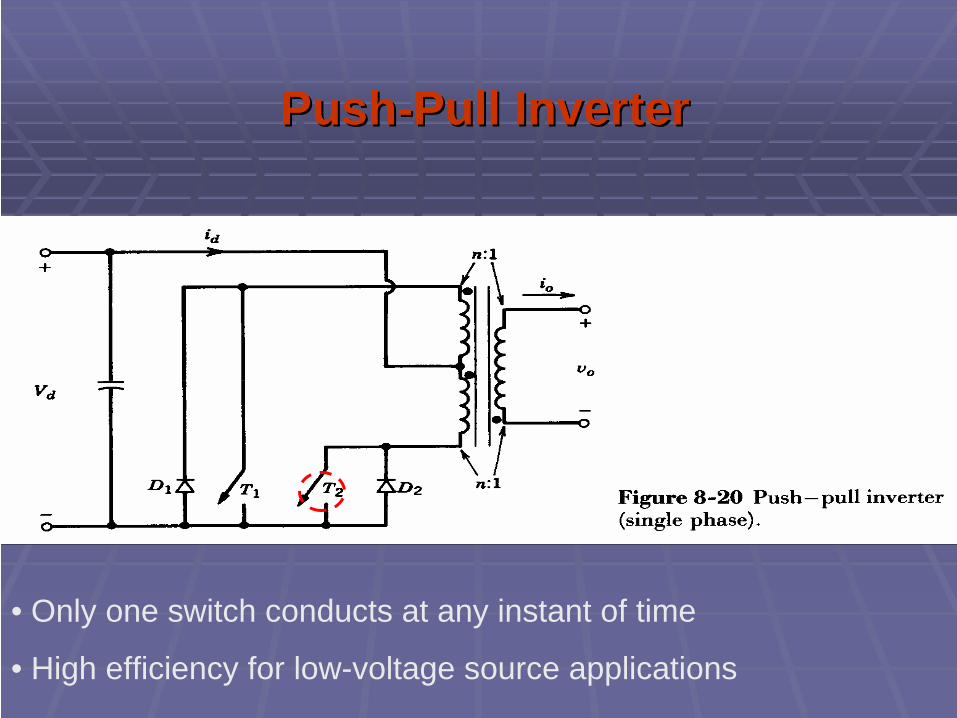
PushPush--Pull InverterPull Inverter
• Only one switch conducts at any instant of time
• High efficiency for low-voltage source applications
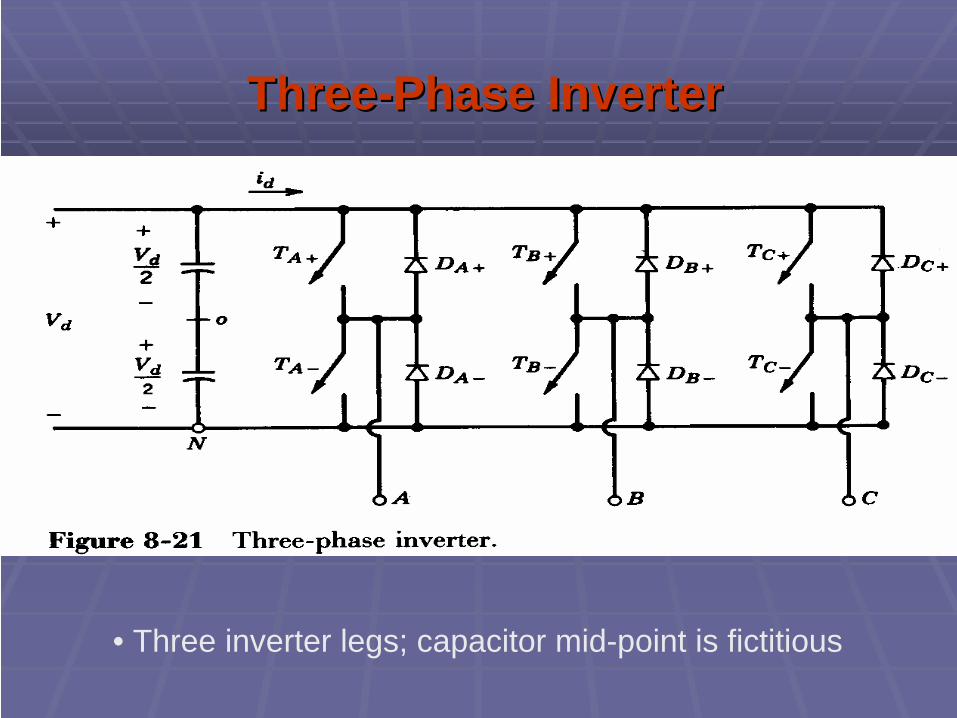
ThreeThree--Phase InverterPhase Inverter
• Three inverter legs; capacitor mid-point is fictitious
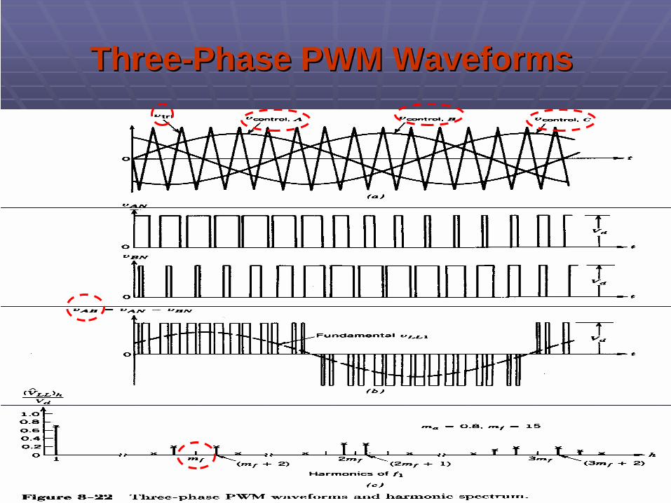
ThreeThree--Phase PWM WaveformsPhase PWM Waveforms
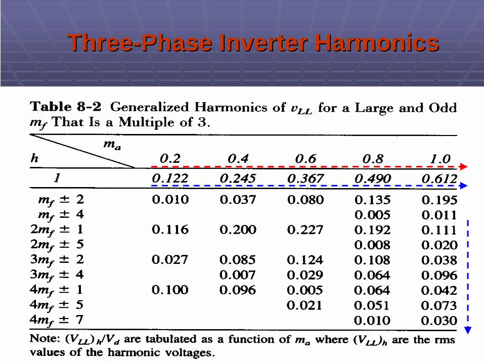
ThreeThree--Phase Inverter HarmonicsPhase Inverter Harmonics
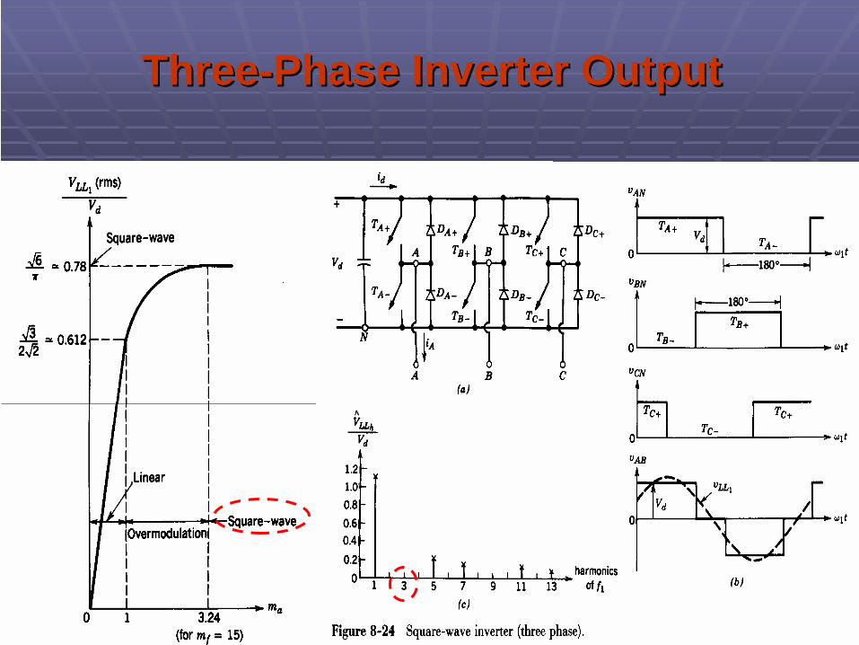
ThreeThree--Phase Inverter OutputPhase Inverter Output
SquareSquare--Wave and PWM OperationWave and PWM Operation
• PWM results in much smaller ripple current

DCDC--Side CurrentSide Currentin a Threein a Three--Phase InverterPhase Inverter
• The current consists of a dc component and the switching-frequency related harmonics

Effect of BlankingEffect of Blanking TimeTime
• Results in nonlinearity
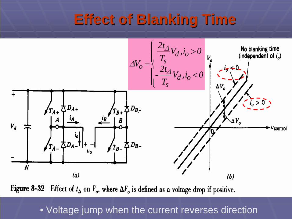
Effect of Blanking TimeEffect of Blanking Time
• Voltage jump when the current reverses direction
⎪⎪⎩
⎪⎪⎨
⎧
<
>=
0i ,VT2t-
0i ,VT2t
Vod
s
ods
oΔ
Δ
Δ
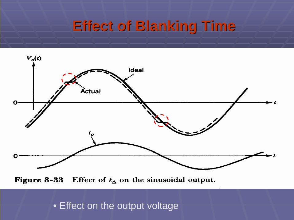
Effect of Blanking TimeEffect of Blanking Time
• Effect on the output voltage
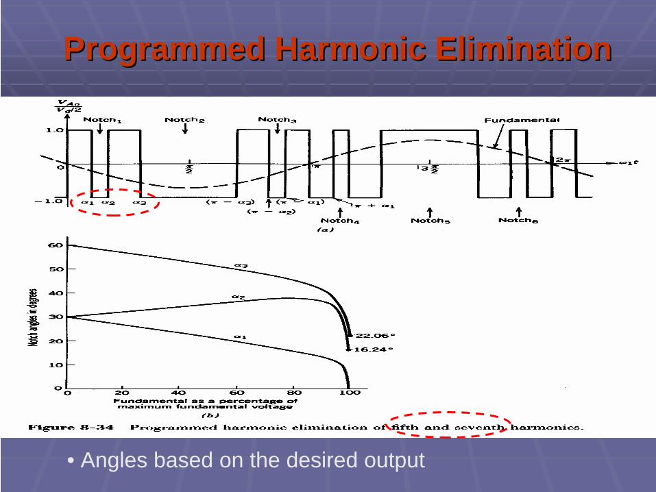
Programmed Harmonic EliminationProgrammed Harmonic Elimination
• Angles based on the desired output

ToleranceTolerance--Band Current ControlBand Current Control
• Results in a variable frequency operation
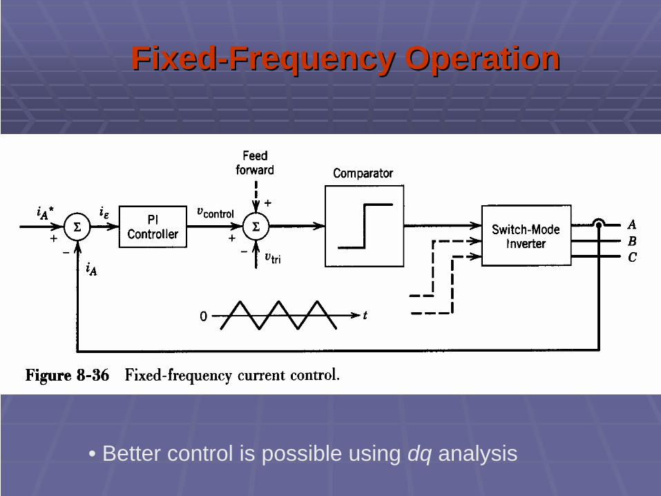
FixedFixed--Frequency OperationFrequency Operation
• Better control is possible using dq analysis
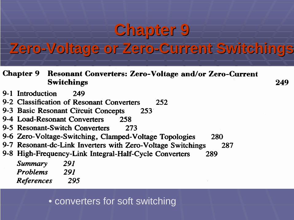
Chapter 9Chapter 9ZeroZero--Voltage or ZeroVoltage or Zero--Current Current SwitchingsSwitchings
• converters for soft switching
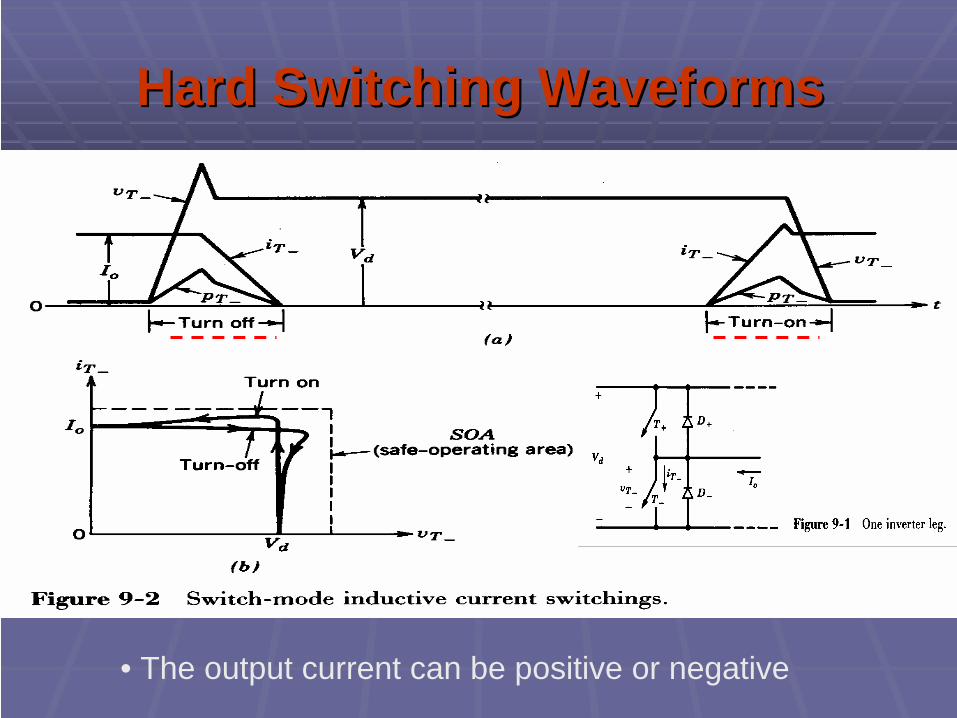
Hard Switching Waveforms Hard Switching Waveforms
• The output current can be positive or negative
TurnTurn--on and Turnon and Turn--off off SnubbersSnubbers

Switching TrajectoriesSwitching Trajectories
• Comparison of Hard versus soft switching
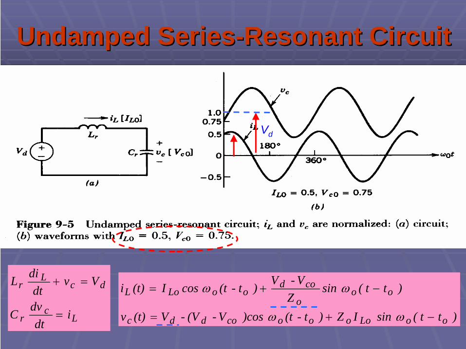
UndampedUndamped SeriesSeries--Resonant Circuit Resonant Circuit
Lc
r
dcL
r
idt
dvC
Vvdt
diL
=
=+
)tt(sinIZ)t-(t)cosV-(V-V(t)v
)tt(sinZ
V-V)t-(tcosI(t)i
ooLoooocoddc
ooo
codooLoL
−+=
−+=
ωω
ωω
Vd

SeriesSeries--Resonant Circuit Resonant Circuit with Capacitorwith Capacitor--Parallel Load Parallel Load
oLc
rc
dcL
r
I-idt
dvCi
Vvdt
diL
==
=+
)tt(sin)I-(IZ)t-(t)cosV-(V-V(t)v
)tt(sinZ
V-V)t-(t)cosI-(II(t)i
oooLoooocoddc
ooo
codoooLooL
−+=
−++=
ωω
ωω

Impedance of a SeriesImpedance of a Series--Resonant Circuit Resonant Circuit
• The impedance is capacitive below the resonance frequency
RZ
RC1
RLQ o
ro
ro ===ω
ω
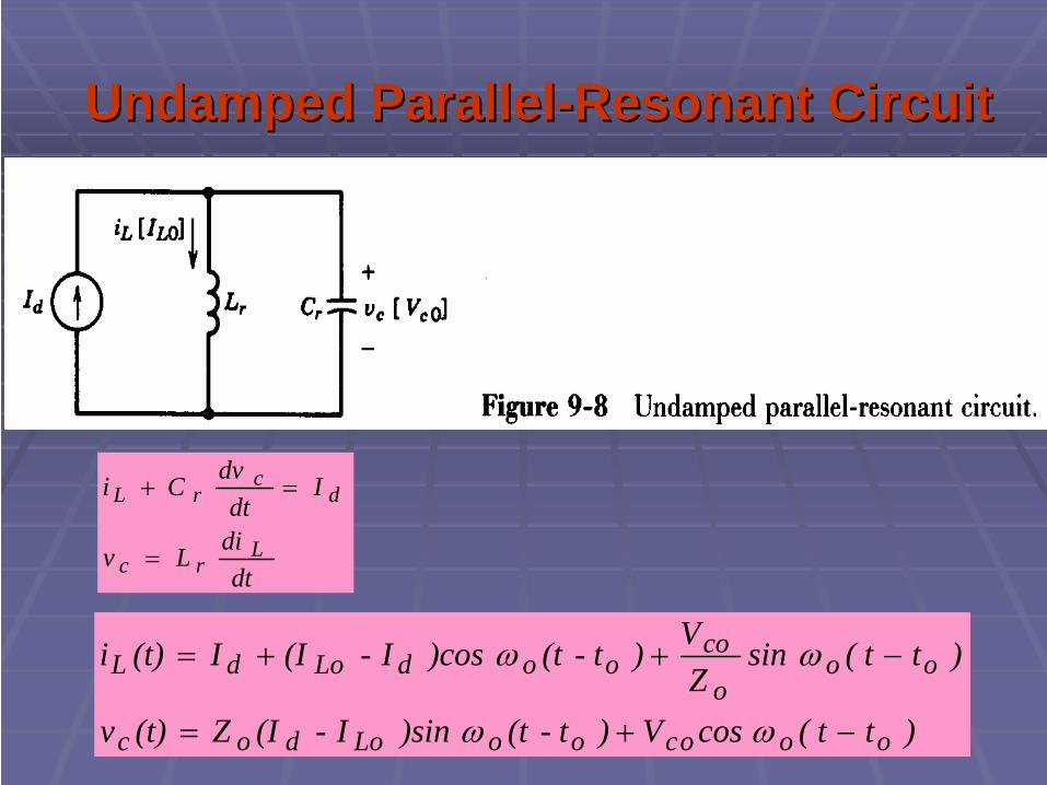
UndampedUndamped ParallelParallel--Resonant Circuit Resonant Circuit
dtdiLv
Idt
dvCi
Lrc
dc
rL
=
=+
)tt(cosV)t-(t)sinI-(IZ(t)v
)tt(sinZ
V)t-(t)cosI-(II(t)i
ooocooLodoc
ooo
cooodLodL
−+=
−++=
ωω
ωω
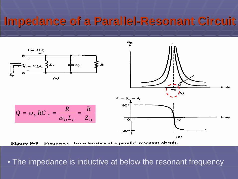
Impedance of a ParallelImpedance of a Parallel--Resonant Circuit Resonant Circuit
• The impedance is inductive at below the resonant frequency
ororo Z
RL
RRCQ ===ω
ω
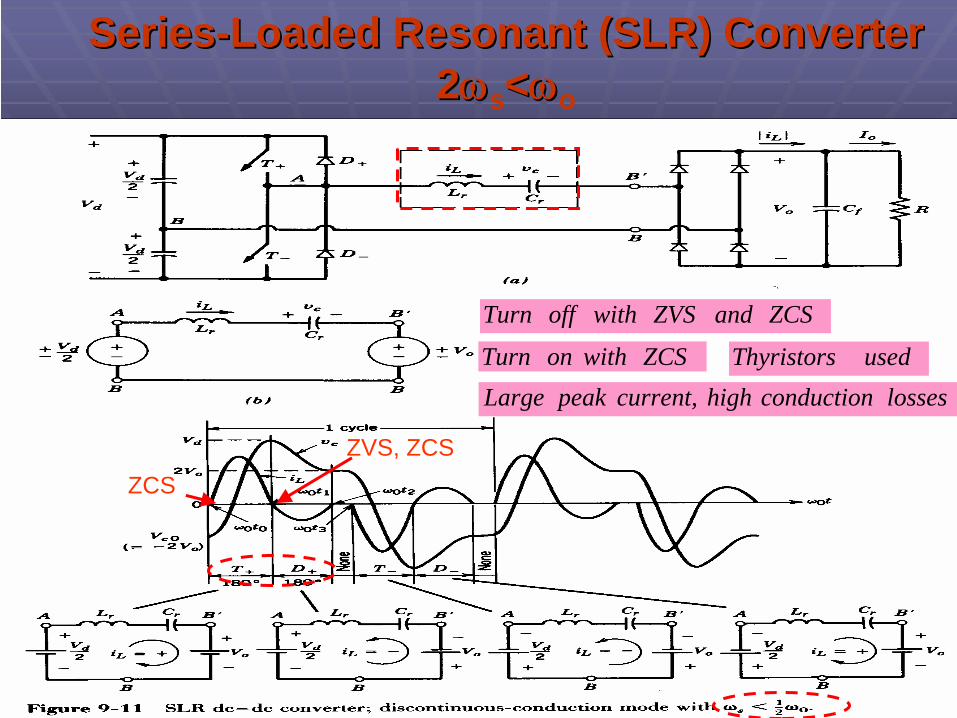
SeriesSeries--Loaded Resonant (SLR) ConverterLoaded Resonant (SLR) Converter22ωωs <<ωωo
ZCSand ZVS withoff Turn
ZCS withon Turnlosses conduction high current, peak Large
used Thyristors
ZCSZVS, ZCS
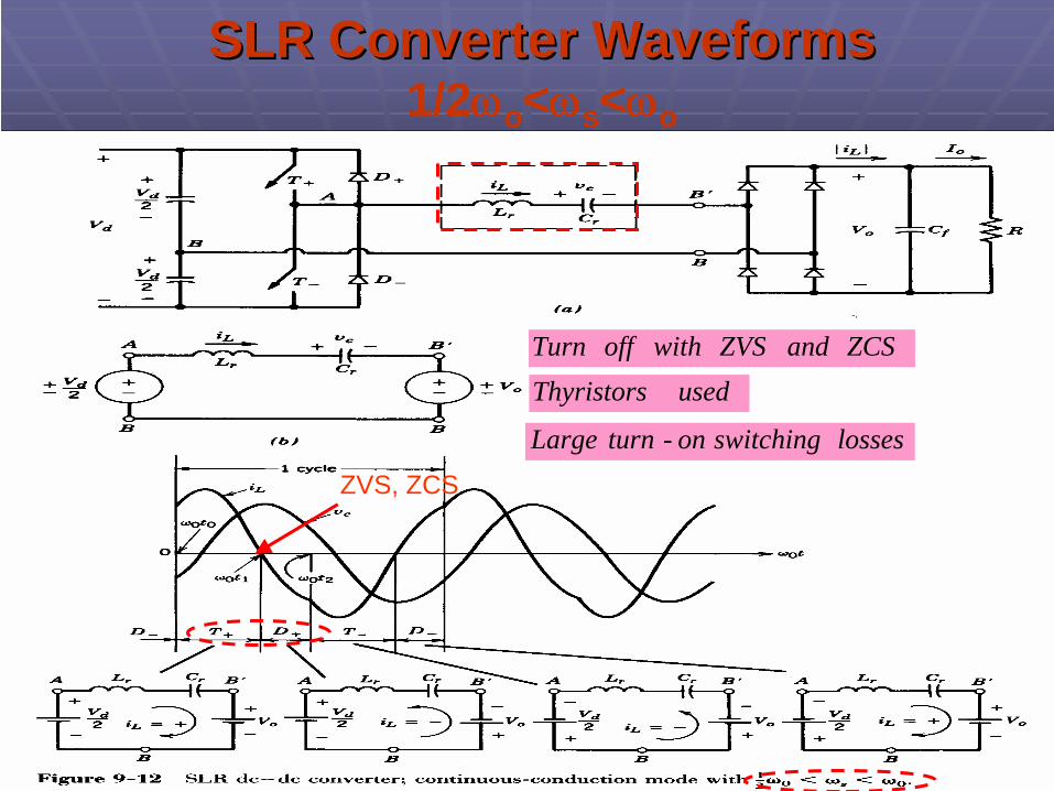
SLR Converter WaveformsSLR Converter Waveforms1/2ωo <ωs <ωo
ZCSand ZVS withoff Turnused Thyristors
losses switchingon-turn LargeZVS, ZCS

SLR SLR Converter WaveformsConverter Waveformsωs >ωo
ZCSand ZVS withon Turnlosses switchingoff-turn Large
used switchesleControllab
ZVS, ZCS

Lossless Snubbers in SLR ConvertersLossless Snubbers in SLR Converters
• The operating frequency is above the resonance frequency

SLR Converter CharacteristicsSLR Converter Characteristics
• The operating frequency is varied to regulate the output voltage
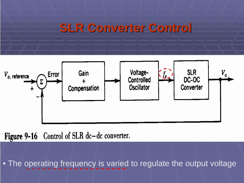
SLR Converter ControlSLR Converter Control
• The operating frequency is varied to regulate the output voltage
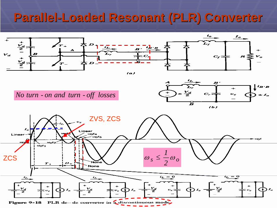
ParallelParallel--Loaded Resonant (PLR) ConverterLoaded Resonant (PLR) Converter
os 21 ωω ≤
losses off-turn and on-turn No
ZVS, ZCS
ZCS
PLR Converter WaveformsPLR Converter Waveforms
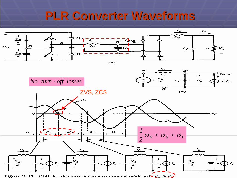
oso21 ωωω <<
losses off-turn No
ZVS, ZCS
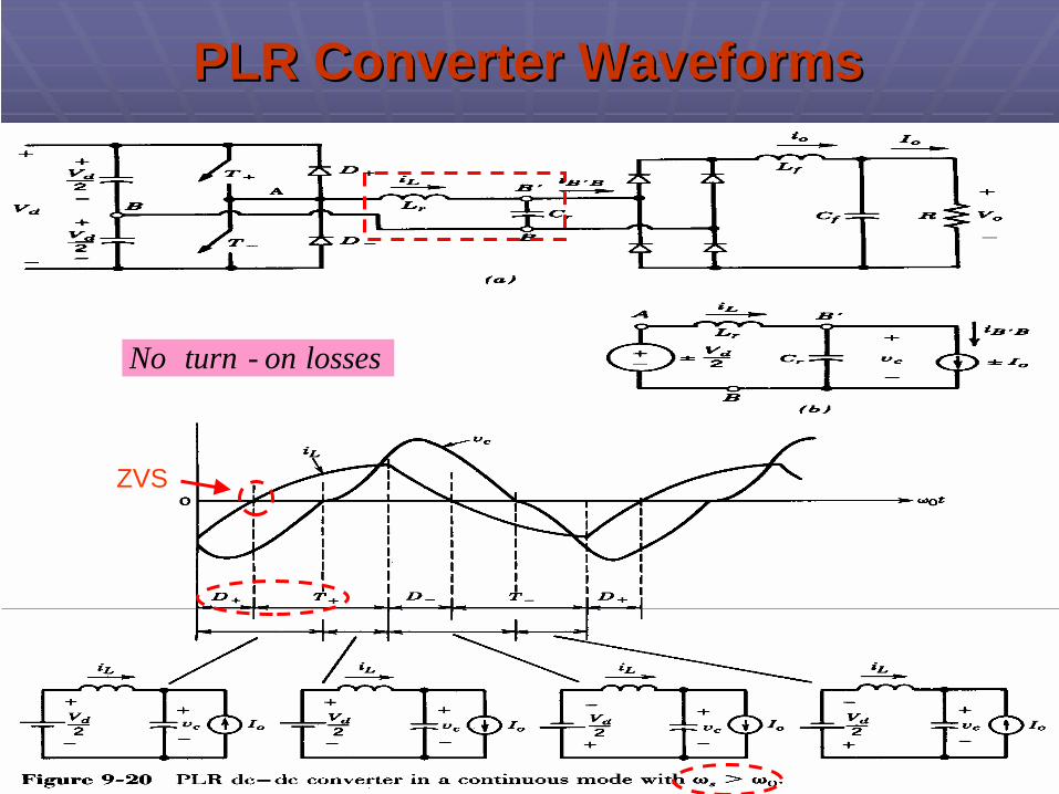
PLR Converter WaveformsPLR Converter Waveforms
losses on-turn No
ZVS
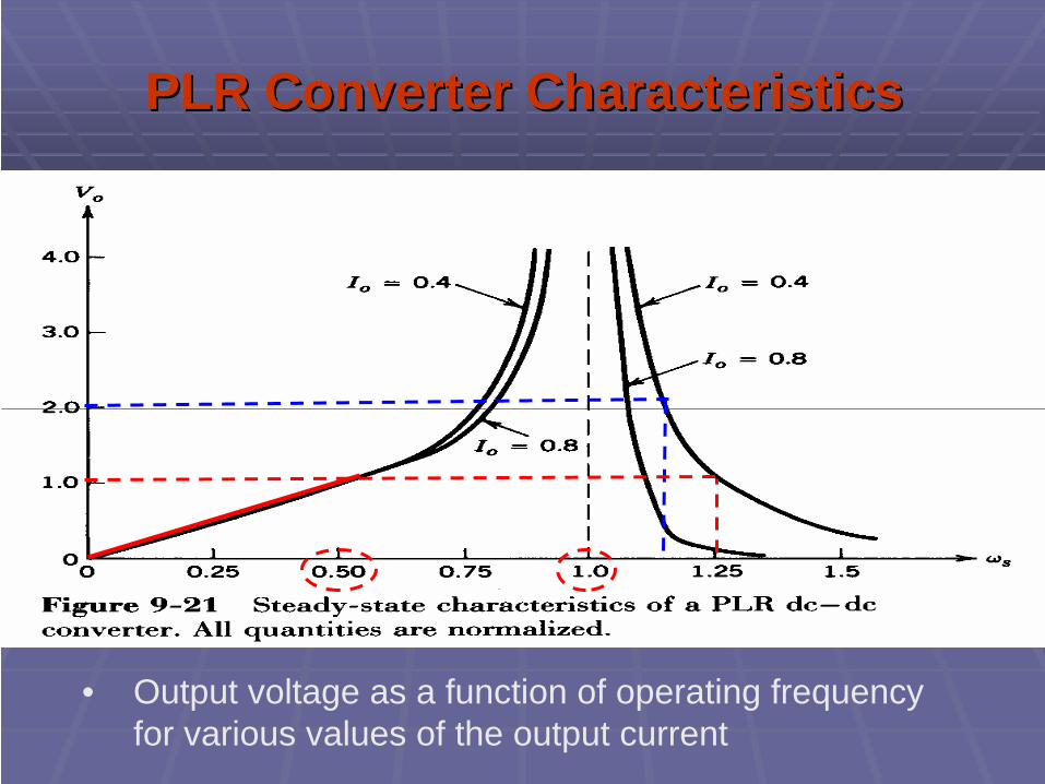
PLR Converter CharacteristicsPLR Converter Characteristics
• Output voltage as a function of operating frequency for various values of the output current

HybridHybrid--Resonant DCResonant DC--DC ConverterDC Converter
• Combination of series- and parallel-loaded resonances
• A SLR offers an inherent current limiting under short-circuit conditions and a PLR regulating its voltage at no load with a high-Q resonant tank is not a problem
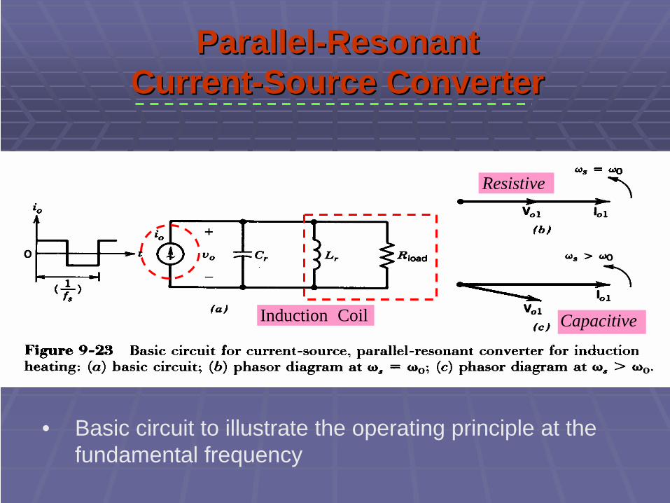
• Basic circuit to illustrate the operating principle at the fundamental frequency
Resistive
CapacitiveCoilInduction
ParallelParallel--ResonantResonantCurrentCurrent--Source ConverterSource Converter
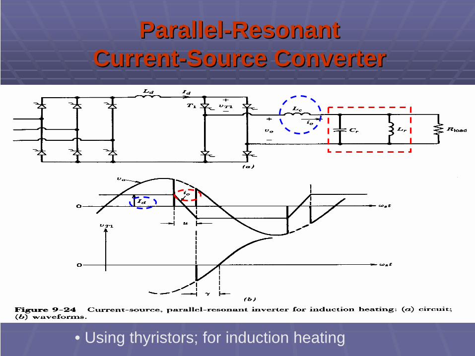
ParallelParallel--ResonantResonantCurrentCurrent--Source ConverterSource Converter
• Using thyristors; for induction heating

ClassClass--E ConvertersE Converters
ballasts electronicfrequency-high for Used
ZCS Turn-on
ZVS Turn-off
Single-switch Sin-wave Current
losses switchingNo
current and volatge peak High
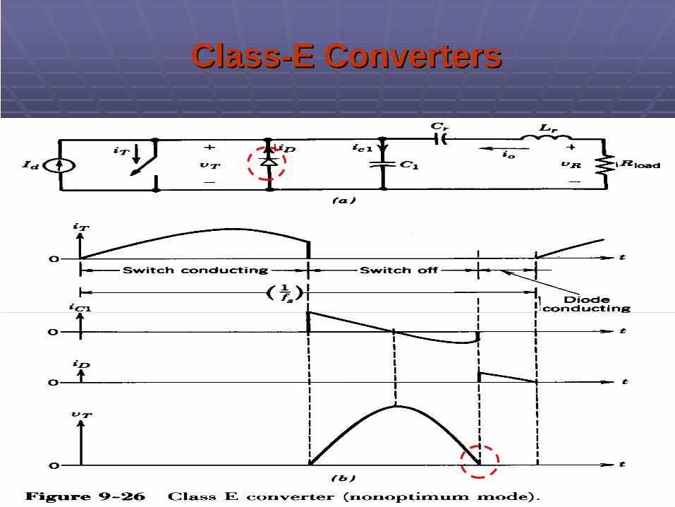
ClassClass--E ConvertersE Converters
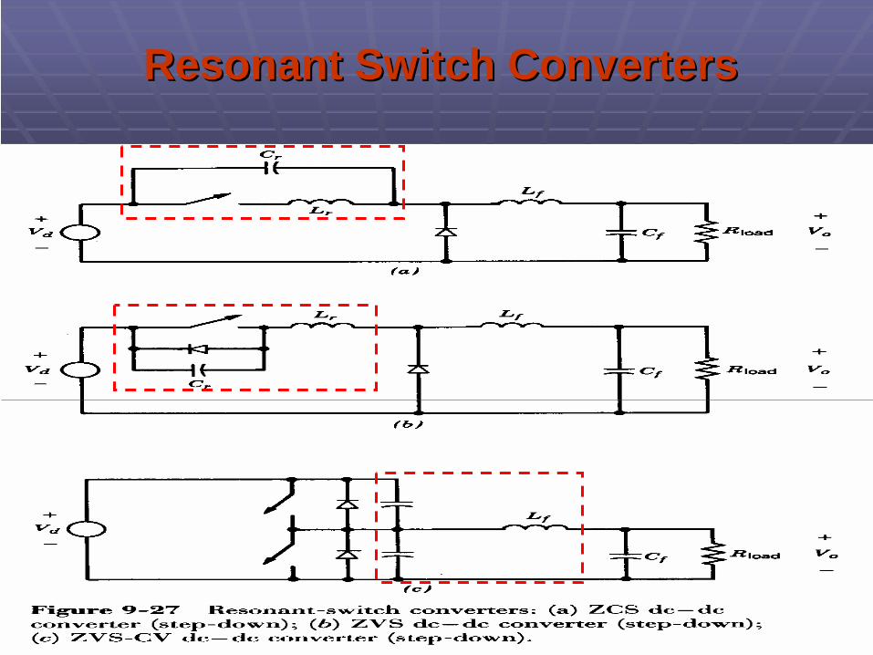
Resonant Switch ConvertersResonant Switch Converters
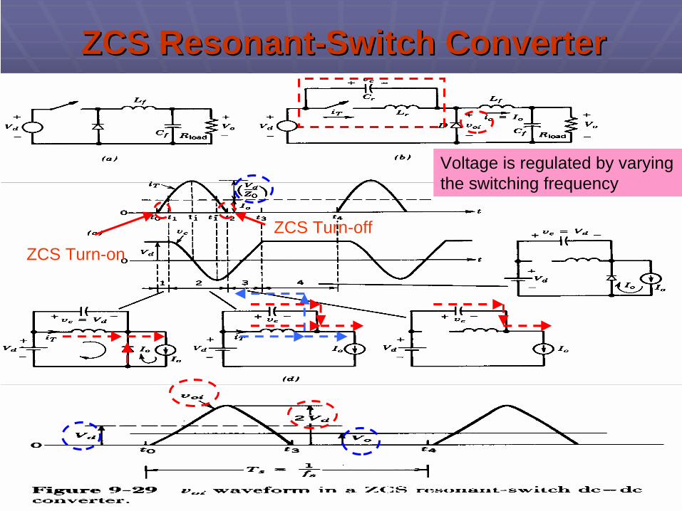
ZCS ResonantZCS Resonant--Switch ConverterSwitch Converter
ZCS Turn-onZCS Turn-off
Voltage is regulated by varying the switching frequency
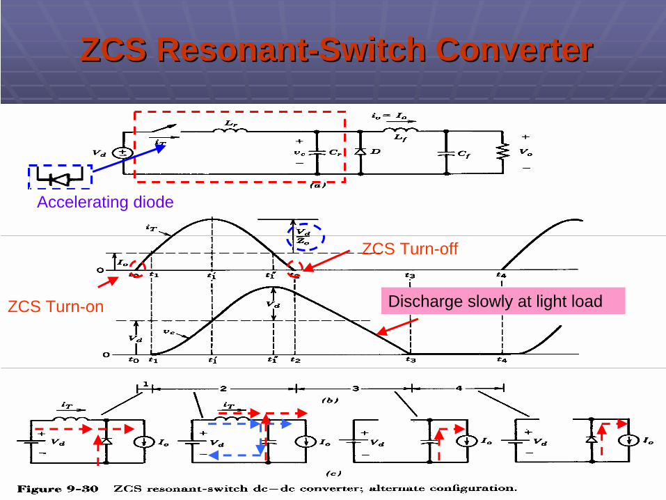
ZCS ResonantZCS Resonant--Switch ConverterSwitch Converter
ZCS Turn-on
ZCS Turn-off
Accelerating diode
Discharge slowly at light load
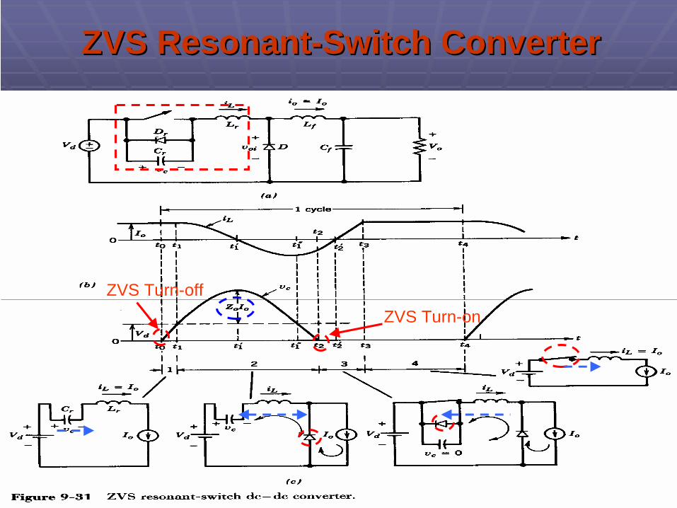
ZVS ResonantZVS Resonant--Switch ConverterSwitch Converter
ZVS Turn-offZVS Turn-on

MOSFET Internal CapacitancesMOSFET Internal Capacitances
• These capacitances affect the MOSFET switching
ZVS is preferable over ZCS at high switching frequencies

ZVSZVS--CV DCCV DC--DC ConverterDC Converter
• The inductor current must reverse direction during each switching cycle
ZVS Turn-on

ZVSZVS--CV DCCV DC--DC ConverterDC Converter
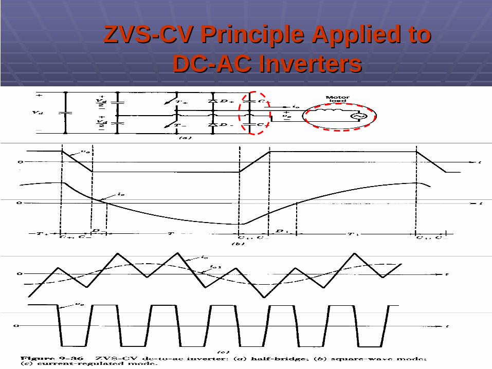
ZVSZVS--CV Principle Applied to CV Principle Applied to DCDC--AC InvertersAC Inverters

ThreeThree--Phase ZVSPhase ZVS--CV DCCV DC--AC InverterAC Inverter
• Very large ripple in the output current
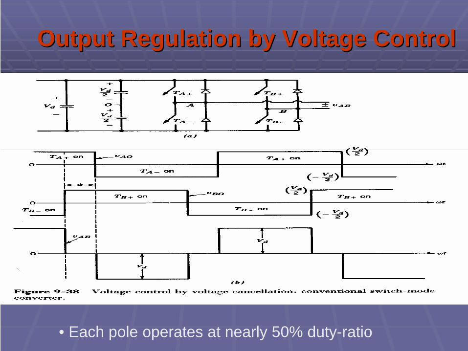
Output Regulation by Voltage ControlOutput Regulation by Voltage Control
• Each pole operates at nearly 50% duty-ratio
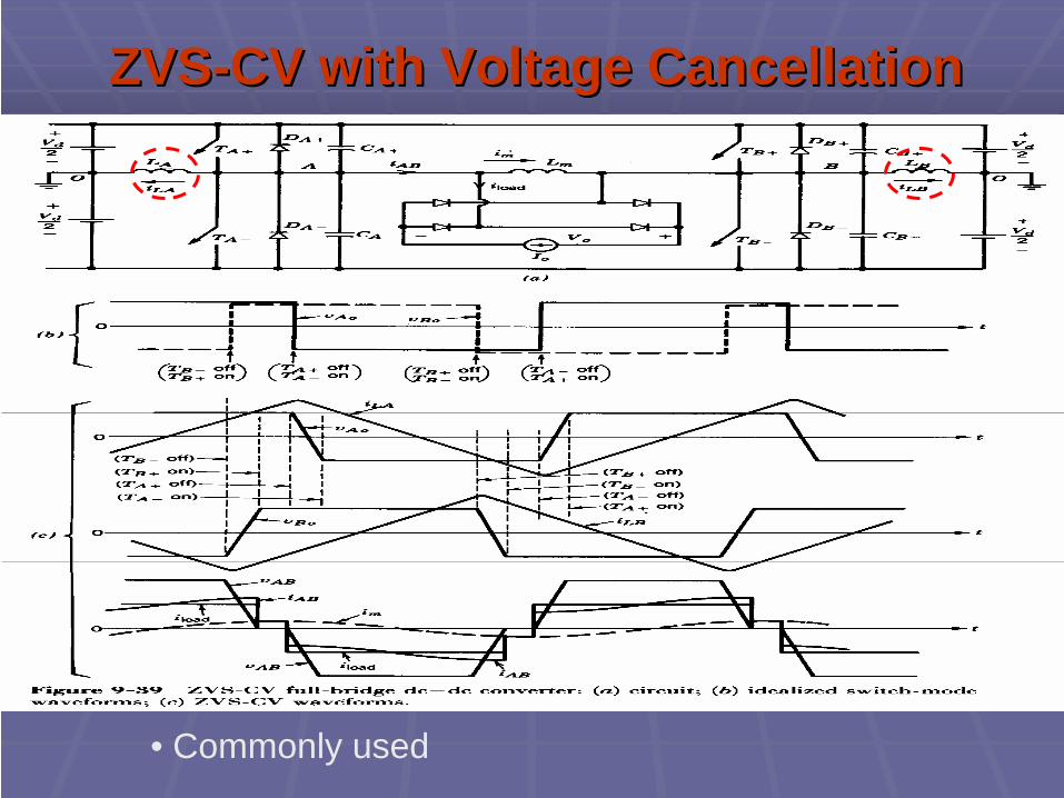
ZVSZVS--CV with Voltage CancellationCV with Voltage Cancellation
• Commonly used

Resonant DCResonant DC--Link InverterLink Inverter
• The dc-link voltage is made to oscillate
ZVS Turn-on
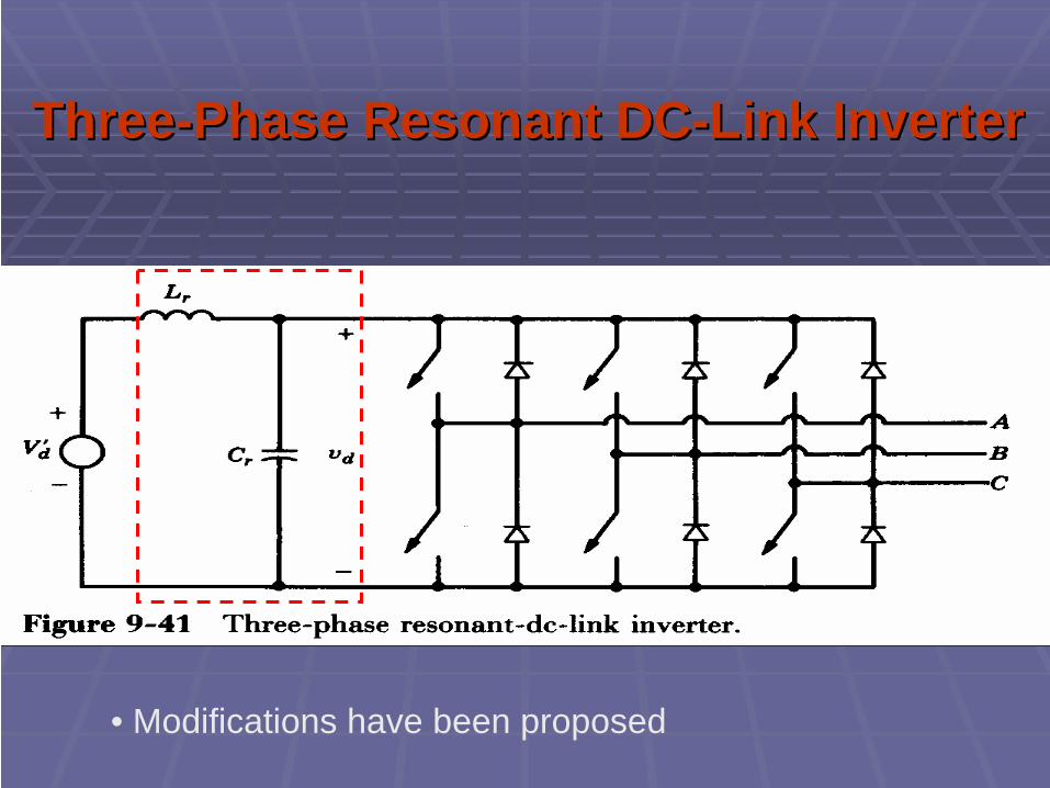
ThreeThree--Phase Resonant DCPhase Resonant DC--Link InverterLink Inverter
• Modifications have been proposed
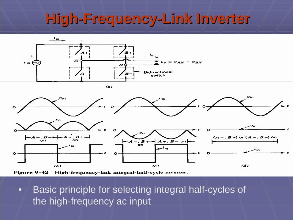
HighHigh--FrequencyFrequency--Link InverterLink Inverter
• Basic principle for selecting integral half-cycles of the high-frequency ac input
HighHigh--FrequencyFrequency--Link InverterLink Inverter
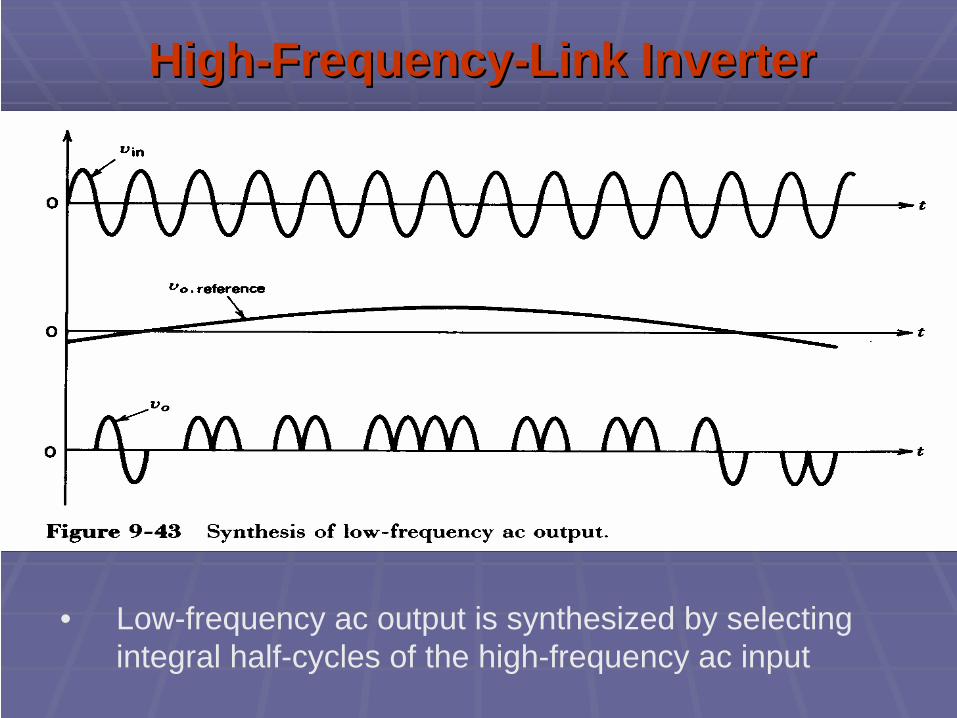
• Low-frequency ac output is synthesized by selecting integral half-cycles of the high-frequency ac input

HighHigh--FrequencyFrequency--Link InverterLink Inverter
• Shows how to implement such an inverter

Chapter 10Chapter 10Switching DC Power SuppliesSwitching DC Power Supplies
• One of the most important applications of power electronics
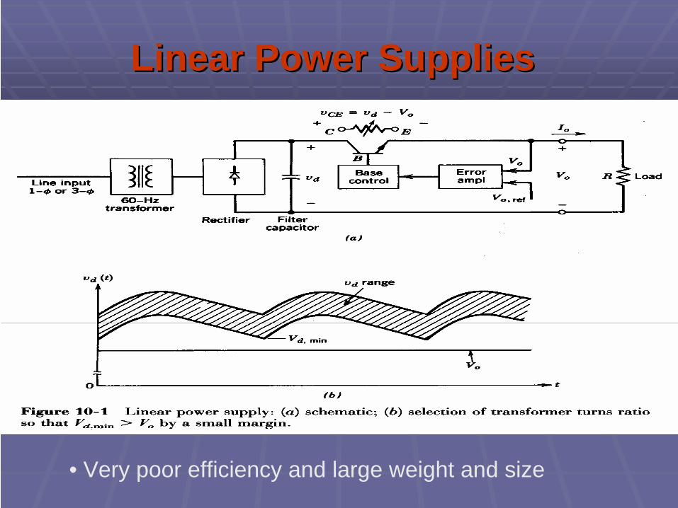
Linear Power SuppliesLinear Power Supplies
• Very poor efficiency and large weight and size
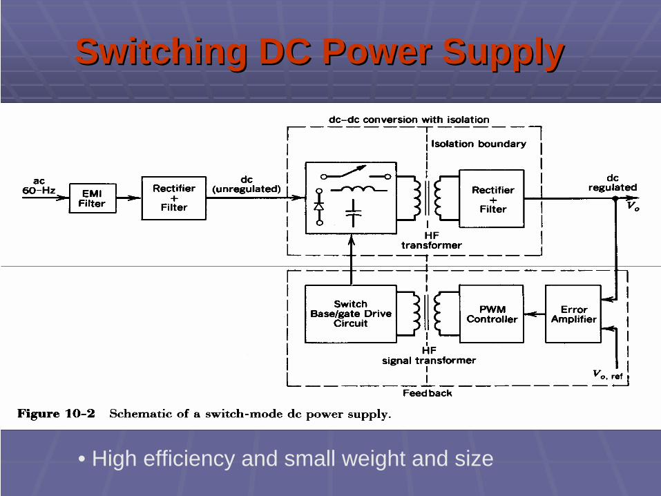
Switching DC Power SupplySwitching DC Power Supply
• High efficiency and small weight and size
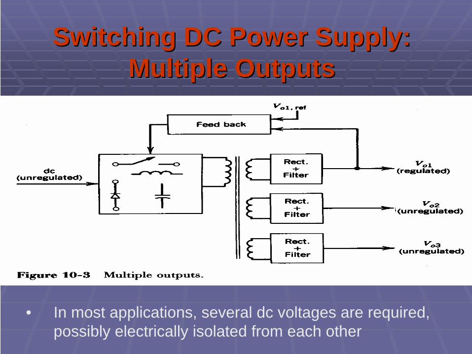
Switching DC Power Supply: Switching DC Power Supply: Multiple OutputsMultiple Outputs
• In most applications, several dc voltages are required, possibly electrically isolated from each other

Transformer AnalysisTransformer Analysis
• Needed to discuss high-frequency isolated supplies
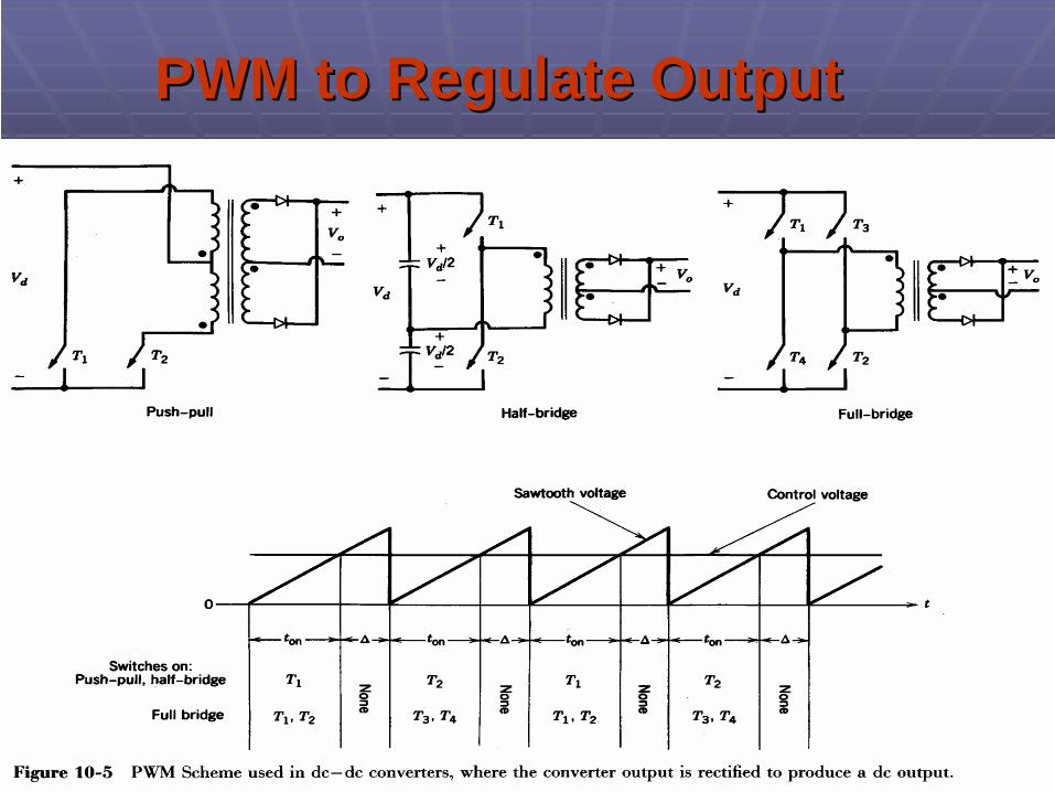
PWM to Regulate OutputPWM to Regulate Output

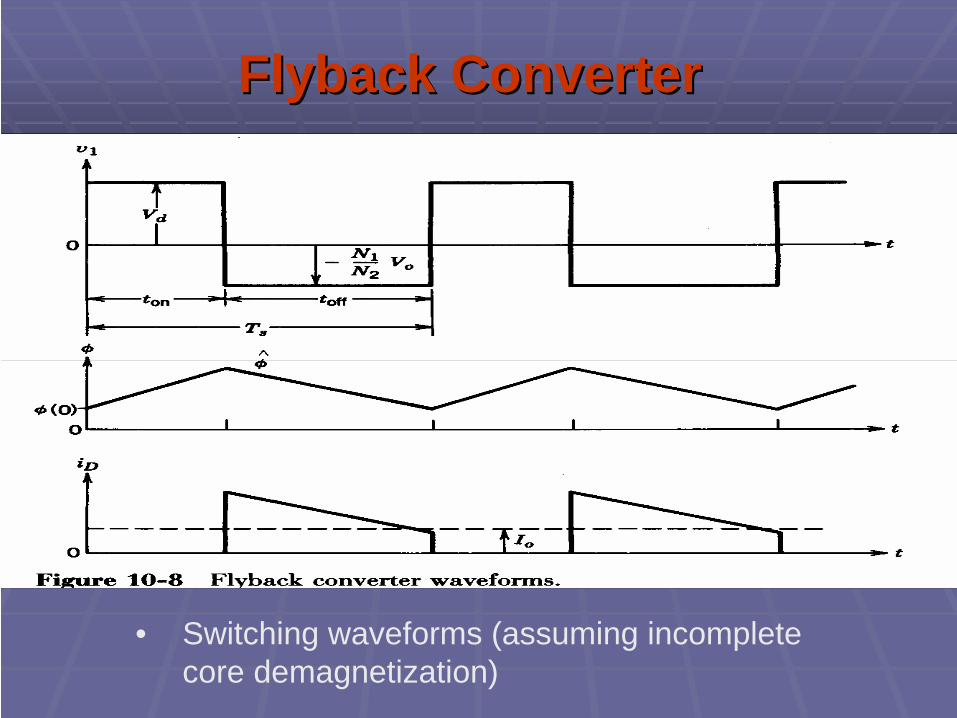
Flyback ConverterFlyback Converter
• Derived from buck-boost; very power at small power (> 50 W ) power levels

Flyback ConverterFlyback Converter
• Switch on and off states (assuming incomplete core demagnetization)
Flyback ConverterFlyback Converter
• Switching waveforms (assuming incomplete core demagnetization)
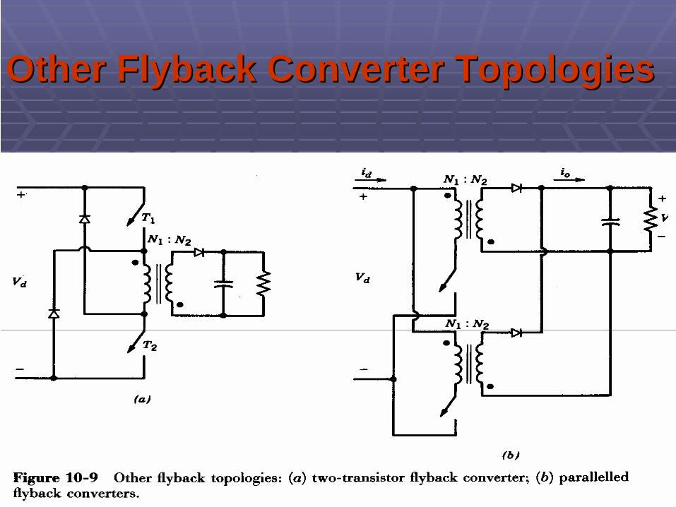
Other Flyback Converter TopologiesOther Flyback Converter Topologies
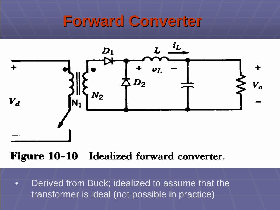
Forward ConverterForward Converter
• Derived from Buck; idealized to assume that the transformer is ideal (not possible in practice)

Forward Converter: in PracticeForward Converter: in Practice
• Switching waveforms (assuming incomplete core demagnetization)
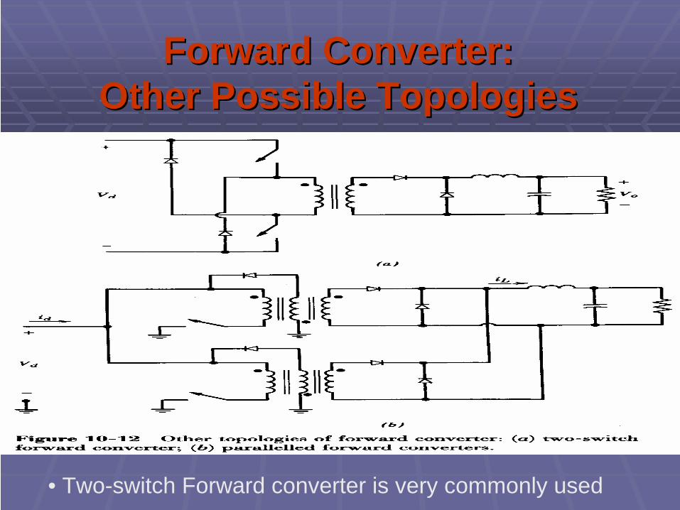
Forward Converter:Forward Converter:Other Possible TopologiesOther Possible Topologies
• Two-switch Forward converter is very commonly used
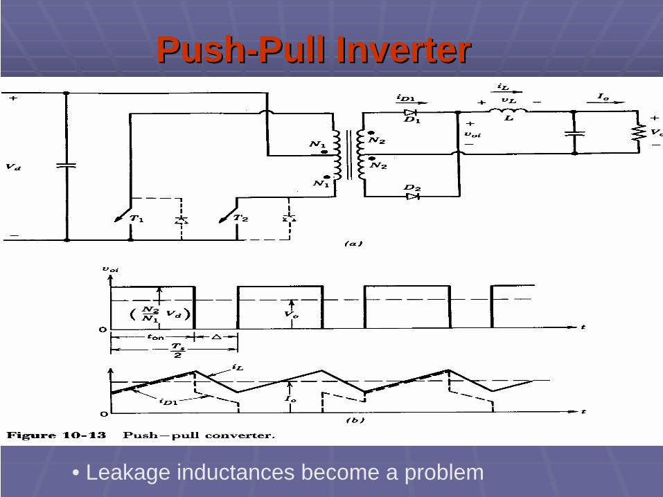
PushPush--Pull InverterPull Inverter
• Leakage inductances become a problem
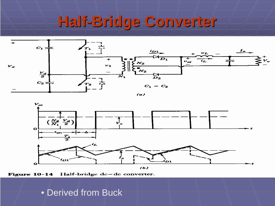
HalfHalf--Bridge ConverterBridge Converter
• Derived from Buck
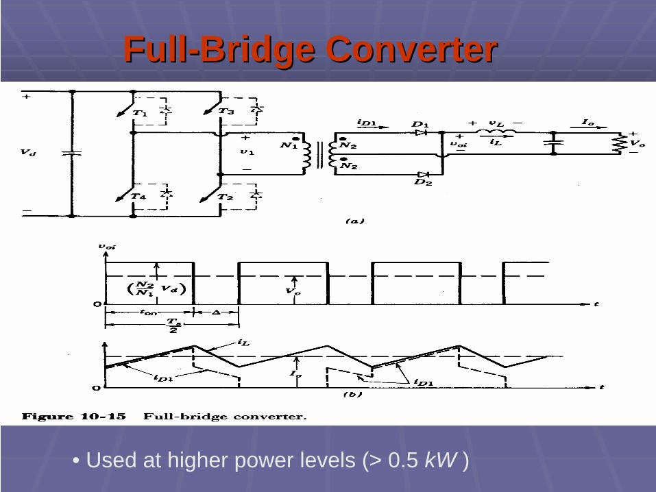
FullFull--Bridge ConverterBridge Converter
• Used at higher power levels (> 0.5 kW )
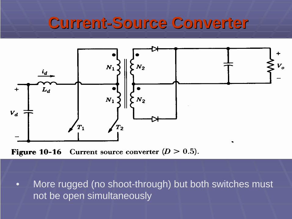
CurrentCurrent--Source ConverterSource Converter
• More rugged (no shoot-through) but both switches must not be open simultaneously

Ferrite Core MaterialFerrite Core Material
• Several materials to choose from based on applications
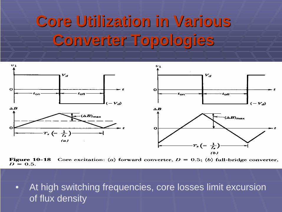
Core Utilization in Various Core Utilization in Various Converter TopologiesConverter Topologies
• At high switching frequencies, core losses limit excursion of flux density

Control to Regulate Voltage OutputControl to Regulate Voltage Output
• Linearized representation of the feedback control system
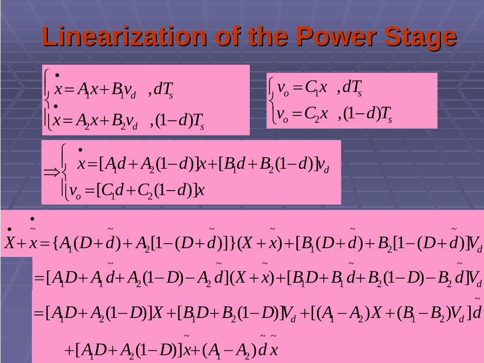
⎪⎩
⎪⎨⎧
−+=
+=•
•
sd
sd
TdvBxAx
dTvBxAx
)1(,
,
22
11
⎩⎨⎧
−==
so
so
TdxCvdTxCv
)1(,,
2
1
⎪⎩
⎪⎨⎧
−+=−++−+=⇒
•
xdCdCvvdBdBxdAdAx
o
d
)]1([)]1([)]1([
21
2121
dVdDBdDBxXdDAdDAxX )](1[)([))]}((1[)({~
2
~
1
~~
2
~
1
~+−+++++−++=+
••
dVdBDBdBDBxXdADAdADA ])1([)]()1([~
22
~
11
~~
22
~
11 −−++++−−++=
~~
21
~
21
~
21212121
)()]1([
])()[()]1([)]1([
xdAAxDADA
dVBBXAAVDBDBXDADA dd
−+−++
−+−+−++−+=
Linearization of the Power StageLinearization of the Power Stage

Linearization of the Power StageLinearization of the Power Stage
~
2121
~~])()[( dVBBXAAxABVAXxX dd −+−+++≈+
••
~
2121
~~])()[( dVBBXAAxAx d−+−+=⇒
•
dBVAXX +==•
0Θ
~~
21
~
21
~
2121
~~
2
~
1
~
)()]1([])[()]1([
])][(1[)({
dxCCxDCDCdXCCXDCDC
xXdDCdDCvV oo
−+−++−+−+=
++−++=+
~~
21
~])[( xCdXCCCXvV oo +−+≈+
CXVo =Θ~
21
~~])[( dXCCxCvo −+=⇒

dBVAXX +==•
0
Linearization of the Power StageLinearization of the Power Stage
CXVand o =BCA
VV
d
o 1−−=⇒Steady-state
DC voltage transfer ratio
~
2121
~~])()[( dVBBXAAxAx d−+−+=
•
)(])()[()()(~
2121
~~sdVBBXAAsxAsxs d−+−+=⇒
)(])()[(][)(~
21211
~sdVBBXAAAsIsx d−+−−=⇒ −
XCCVBBXAAAsICsd
svsT do
p )(])()[(][)(
)()( 2121211
~
~
−+−+−−==⇒ −
~
21
~~])[( dXCCxCvo −+=

Forward Converter: An ExampleForward Converter: An Example
⎪⎩
⎪⎨⎧
=−++−
=−+++−••
••
0)(
0)(
2122
2111
xCxRxCrx
xCxRxrxLV
c
Ld
d
cc
cc
LcLc
VLxx
rRCrRCR
rRLR
rRLrrRrRr
x
x⎥⎥
⎦
⎤
⎢⎢
⎣
⎡+⎥⎦
⎤⎢⎣
⎡
⎥⎥⎥⎥
⎦
⎤
⎢⎢⎢⎢
⎣
⎡
+−
+
+−
+++
−=
⎥⎥
⎦
⎤
⎢⎢
⎣
⎡•
•
0
1
)(1
)(
)()(2
1
2
1
A1 =A2 B1
B2 =0

⎥⎦
⎤⎢⎣
⎡⎥⎦
⎤⎢⎣
⎡++
=−=•
2
121 )(
xx
rRR
rRRrxCxRv
cc
co
C1 =C2
111 ,, CCDBBAA ===⇒
⎥⎥⎥
⎦
⎤
⎢⎢⎢
⎣
⎡
−
−+
−≈==
CRC
LLrr
AAALc
11
1
21
[ ]121 crCCC ≈==
⇒+>> )( LC rrRD
LDBB ⎥
⎦
⎤⎢⎣
⎡==
0/1
1
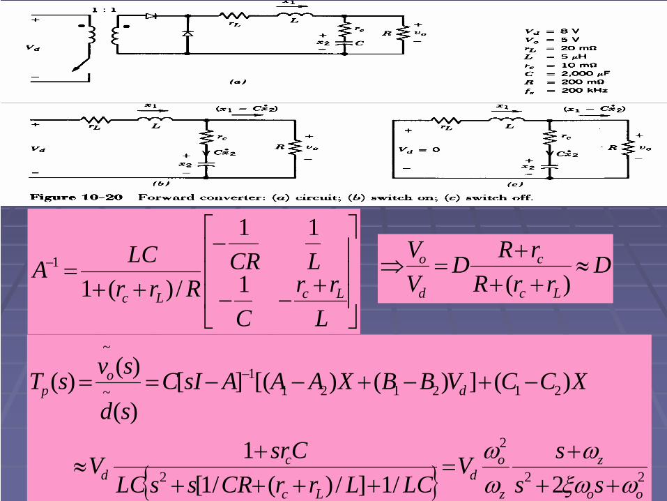
⎥⎥⎥
⎦
⎤
⎢⎢⎢
⎣
⎡
+−−
−
++=−
Lrr
C
LCRRrr
LCALcLc
1
11
/)(11 D
rrRrRD
VV
Lc
c
d
o ≈++
+=⇒
)(
{ } 22
2
2
2121211
~
~
2/1]/)(/1[1
)(])()[(][)(
)()(
oo
z
z
od
Lc
cd
do
p
sssV
LCLrrCRssLCCsrV
XCCVBBXAAAsICsd
svsT
ωξωω
ωω
+++
=++++
+≈
−+−+−−== −

Forward Converter:Forward Converter:Transfer Function PlotsTransfer Function Plots
22
2
2)(
oo
z
z
odp ss
sVsTωξω
ωωω
+++
=
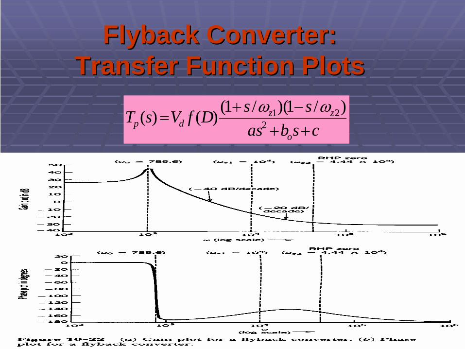
Flyback Converter:Flyback Converter:Transfer Function PlotsTransfer Function Plots
csbasssDfVsT
o
zzdp ++
−+= 2
21 )/1)(/1()()( ωω

LinearizingLinearizing the PWM Blockthe PWM Block
^~
~1
)(
)()(rc
m
Vsv
sdsT == )()()(
)(
)(
)(
)(
)()( ~
~
~
~
~
~
sTsTsv
sd
sd
sv
sv
svsT mp
c
o
c
ol ===⇒

Typical Gain and Phase Plots of the Typical Gain and Phase Plots of the OpenOpen--Loop Transfer FunctionLoop Transfer Function
• Definitions of the crossover frequency, phase and gain margins

A General Amplifier for A General Amplifier for Error CompensationError Compensation
• Can be implemented using a single op-amp
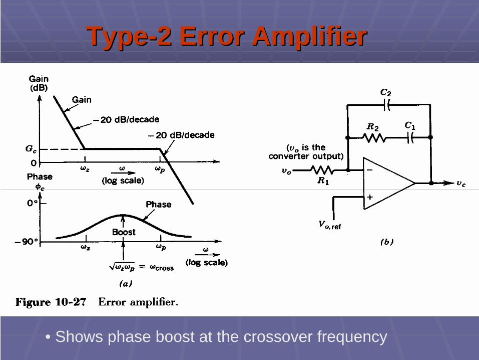
TypeType--2 Error Amplifier2 Error Amplifier
• Shows phase boost at the crossover frequency
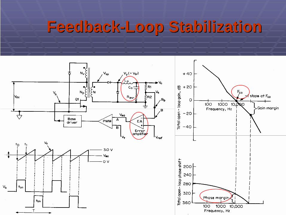
FeedbackFeedback--Loop StabilizationLoop Stabilization

FeedbackFeedback--Loop StabilizationLoop Stabilization
co
p
z
co
FF
FFK ==
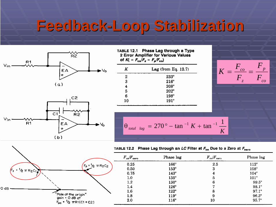
FeedbackFeedback--Loop StabilizationLoop Stabilization
co
p
z
co
FF
FFK ==
KKlagtotal
1tantan270 11 −− +−°=θ

Compensator Design ExampleCompensator Design ExampleVVoo 5V5VIIo(nomo(nom) ) 10A10AIIo(mino(min) ) 1A1ASwitching frequency Switching frequency 100kHz100kHzMinimum output ripple Minimum output ripple 50mV50mVPP--PP
HI
TVLon
oo μ15
101010533 6
=×××
==−
FVdIC
oro μ2600
05.0210651065 66 =××=×= −−
HzCL
Foo
o 8062
1==
π
kHzCR
Foesr
esr 5.210652
12
16 =
××== −ππ

Compensator Design ExampleCompensator Design ExampledB
VG sp
m 5.43
)111(5.03
)1(5.0+=
−×=
−=
dBGG sm 5.165.4)55.2log(205.4 −=−=+=+
Ω=×=×= kkdBRR 1001001)40(10012
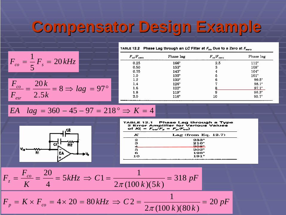
Compensator Design ExampleCompensator Design Example
°=⇒== 9785.2
20 lagkk
FF
esr
co
42189745360 =⇒°=−−= KlagEA
kHzFF sco 2051
==
pFkk
CkHzKFF co
z 318)5)(100(2
1154
20==⇒===
π
pFkk
CkHzFKF cop 20)80)(100(2
1280204 ==⇒=×=×=π

Voltage FeedVoltage Feed--Forward Forward
• Makes converter immune from input voltage variations

Voltage versus Current Mode ControlVoltage versus Current Mode Control

Various Types of Current Mode Control Various Types of Current Mode Control
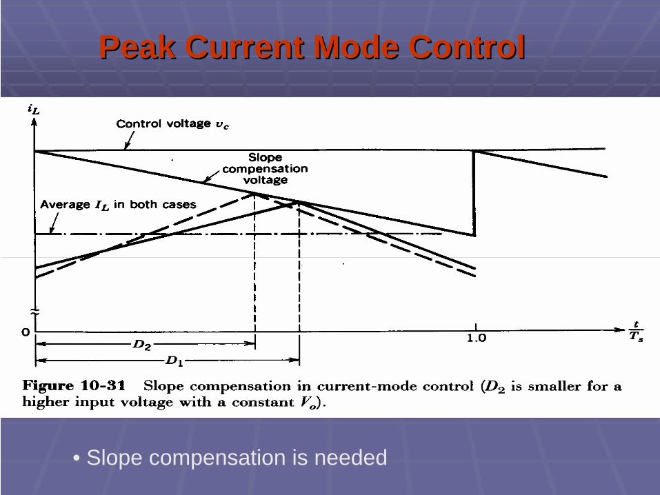
Peak Current Mode ControlPeak Current Mode Control
• Slope compensation is needed
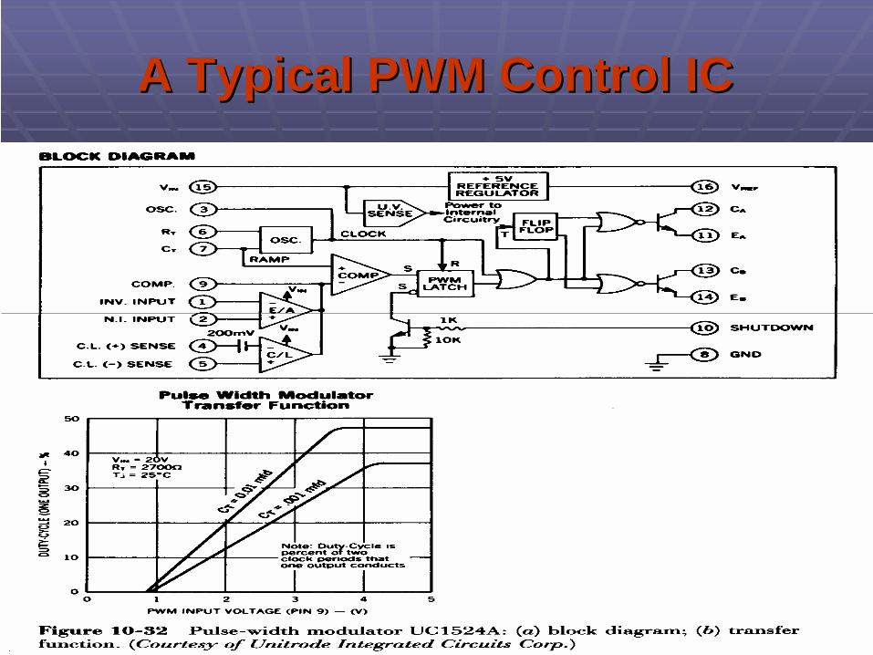
A Typical PWM Control ICA Typical PWM Control IC
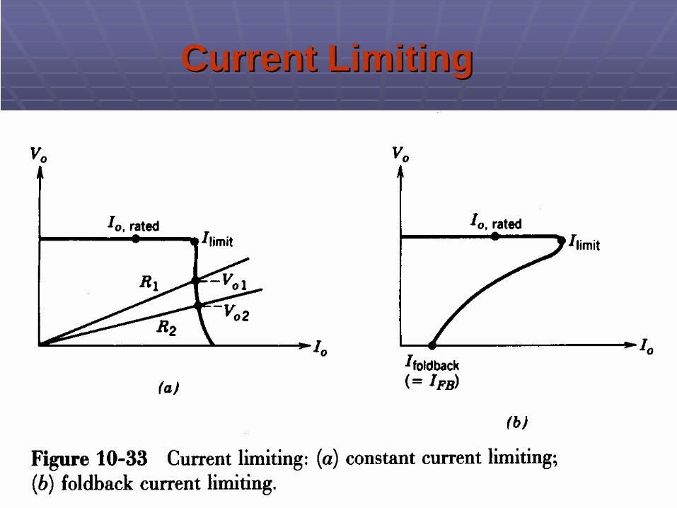
Current LimitingCurrent Limiting

Implementing Electrical Isolation Implementing Electrical Isolation in the Feedback Loopin the Feedback Loop

Implementing Electrical Isolation Implementing Electrical Isolation in the Feedback Loopin the Feedback Loop
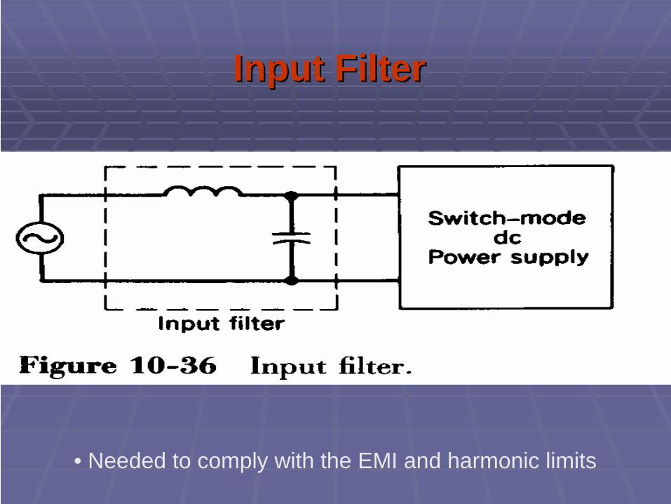
Input FilterInput Filter
• Needed to comply with the EMI and harmonic limits

ESR of the Output CapacitorESR of the Output Capacitor
• ESR often dictates the peak-peak voltage ripple

Chapter 11Chapter 11Power Conditioners and Power Conditioners and
Uninterruptible Power SuppliesUninterruptible Power Supplies
• Becoming more of a concern as utility de-regulation proceeds

Distortion in the Input VoltageDistortion in the Input Voltage
• The voltage supplied by the utility may not be sinusoidal

Typical Voltage Tolerance Typical Voltage Tolerance Envelope for Computer SystemsEnvelope for Computer Systems
• This has been superceded by a more recent standard
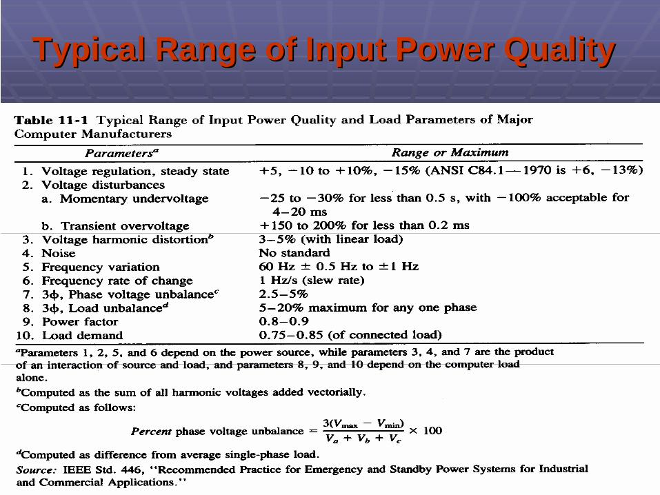
Typical Range of Input Power QualityTypical Range of Input Power Quality
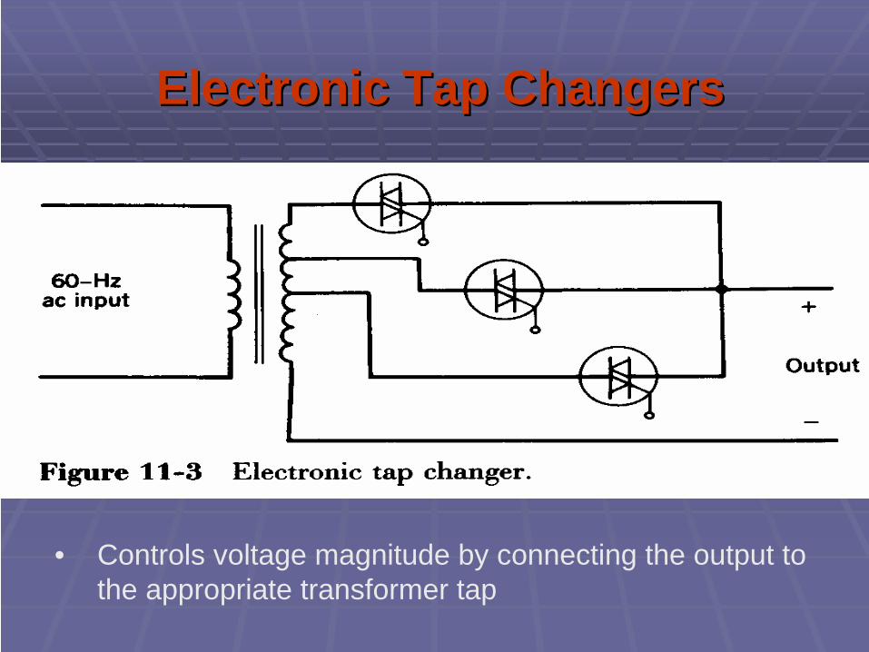
Electronic Tap ChangersElectronic Tap Changers
• Controls voltage magnitude by connecting the output to the appropriate transformer tap

Uninterruptible Power Supplies Uninterruptible Power Supplies (UPS)(UPS)
• Block diagram; energy storage is shown to be in batteries but other means are being investigated

UPS: Possible Rectifier ArrangementsUPS: Possible Rectifier Arrangements
• The input normally supplies power to the load as well as charges the battery bank

UPS: Another Possible Rectifier UPS: Another Possible Rectifier ArrangementArrangement
• Consists of a high-frequency isolation transformer

UPS: Another Possible Input UPS: Another Possible Input ArrangementArrangement
• A separate small battery charger circuit

Battery Charging Waveforms as Battery Charging Waveforms as Function of TimeFunction of Time
• Initially, a discharged battery is charged with a constant current

UPS: Various Inverter ArrangementsUPS: Various Inverter Arrangements
• Depends on applications, power ratings
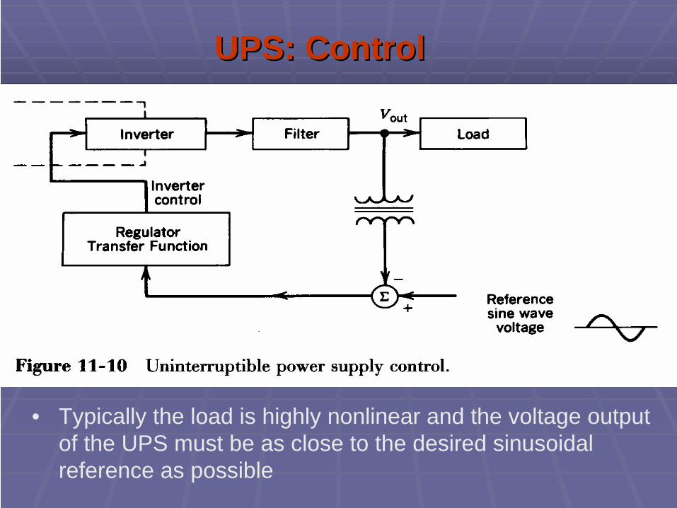
UPS: ControlUPS: Control
• Typically the load is highly nonlinear and the voltage output of the UPS must be as close to the desired sinusoidal reference as possible
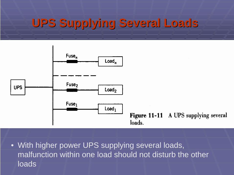
UPS Supplying Several LoadsUPS Supplying Several Loads
• With higher power UPS supplying several loads, malfunction within one load should not disturb the other loads
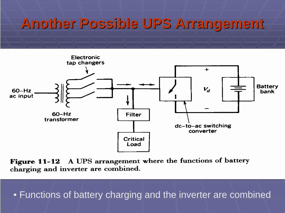
Another Possible UPS ArrangementAnother Possible UPS Arrangement
• Functions of battery charging and the inverter are combined

UPS: Using the Line Voltage as BackupUPS: Using the Line Voltage as Backup
• Needs static transfer switches

Chapter 16Chapter 16Residential and Industrial ApplicationsResidential and Industrial Applications
• Significant in energy conservation; productivity

Inductive Ballast of Fluorescent LampsInductive Ballast of Fluorescent Lamps
• Inductor is needed to limit current
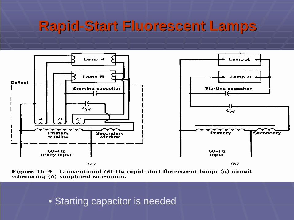
RapidRapid--Start Fluorescent LampsStart Fluorescent Lamps
• Starting capacitor is needed

Electronic Ballast for Fluorescent LampsElectronic Ballast for Fluorescent Lamps
• Lamps operated at ~40 kHz
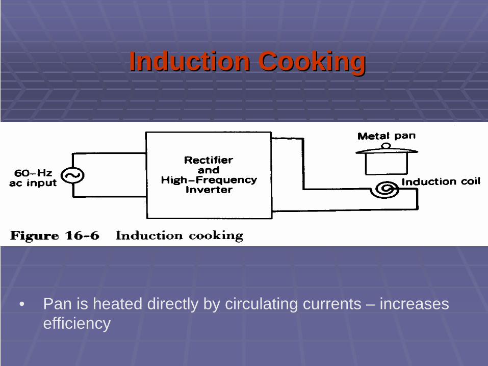
Induction CookingInduction Cooking
• Pan is heated directly by circulating currents – increases efficiency
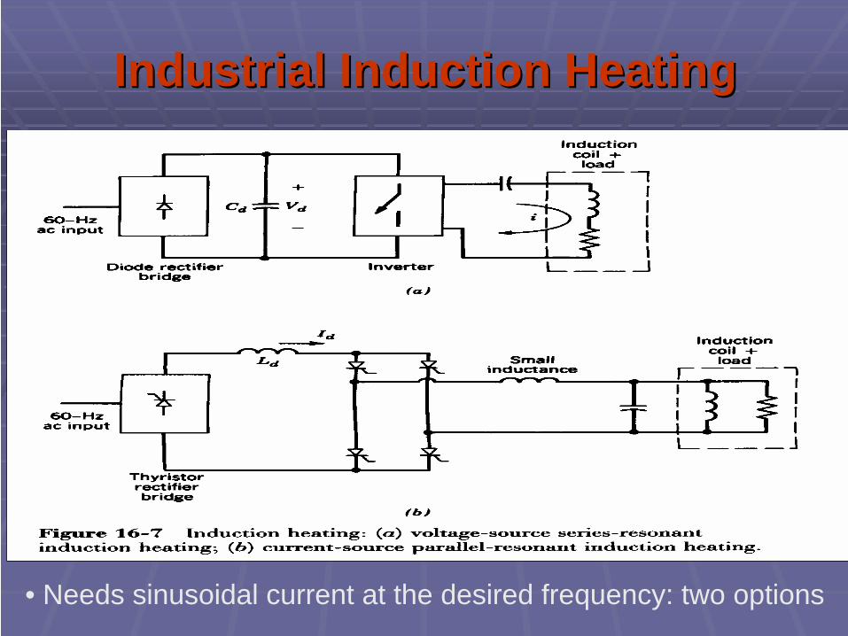
Industrial Induction HeatingIndustrial Induction Heating
• Needs sinusoidal current at the desired frequency: two options
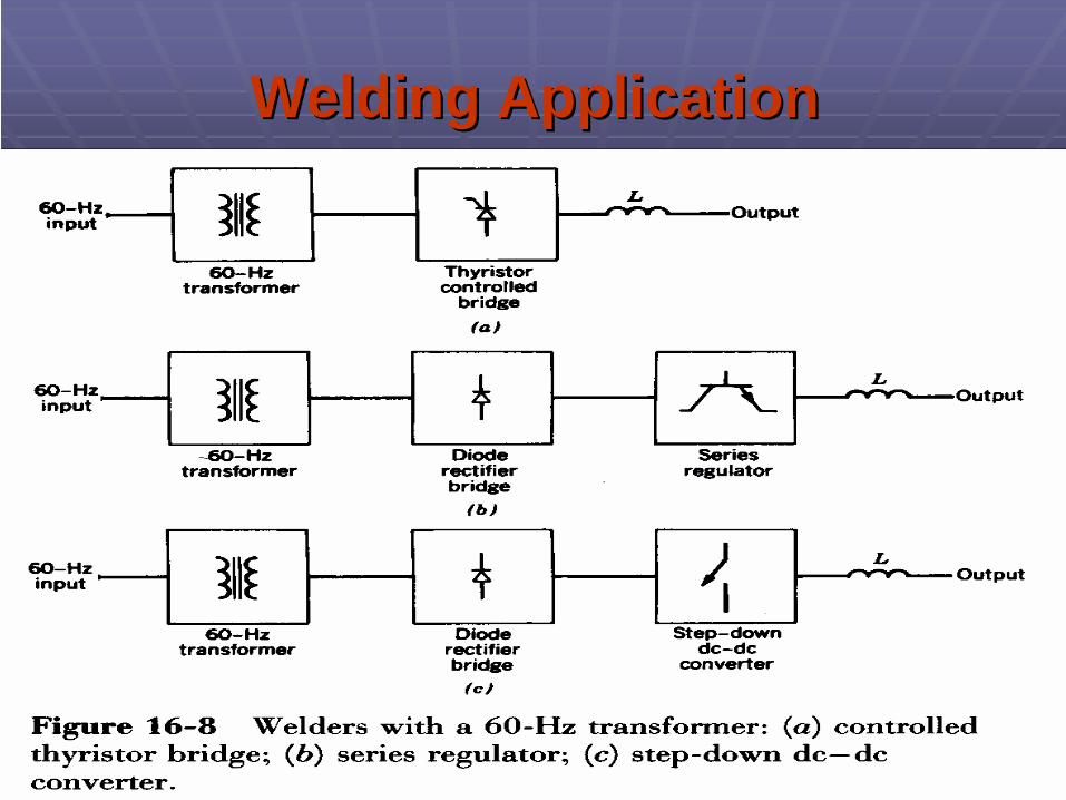
Welding ApplicationWelding Application

SwitchSwitch--Mode WeldersMode Welders
• Can be made much lighter weight

Chapter 17Chapter 17Electric Utility ApplicationsElectric Utility Applications
• These applications are growing rapidly
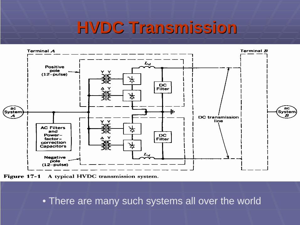
HVDC TransmissionHVDC Transmission
• There are many such systems all over the world
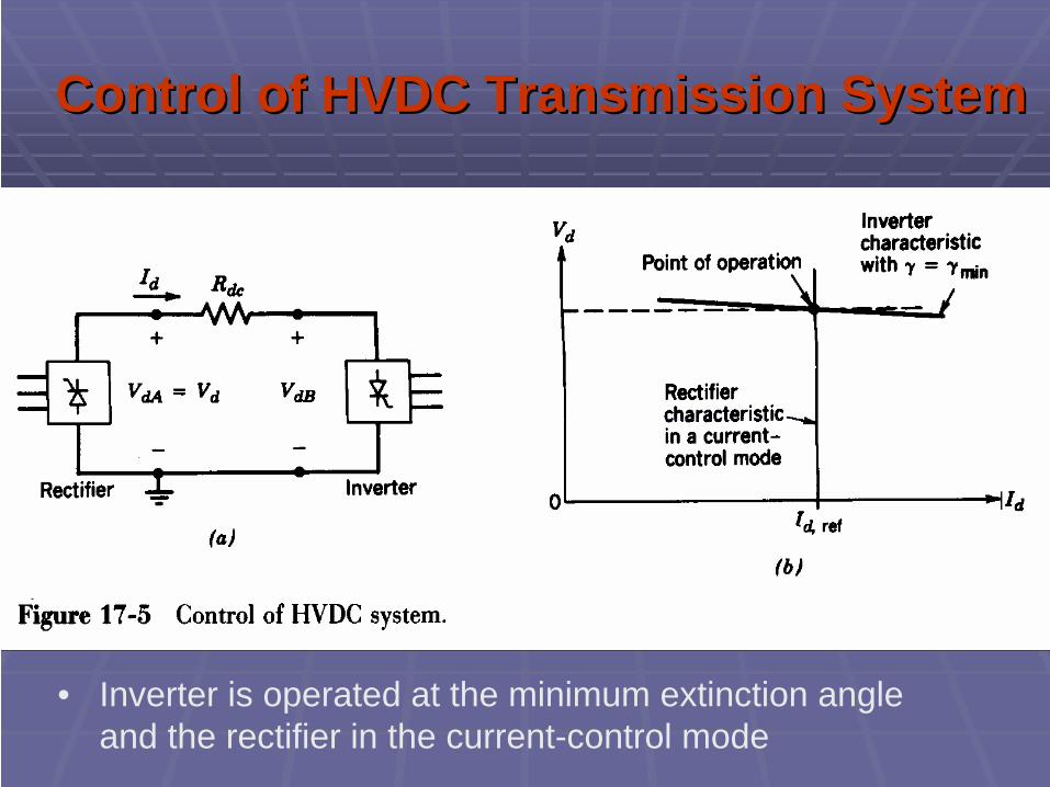
Control of HVDC Transmission SystemControl of HVDC Transmission System
• Inverter is operated at the minimum extinction angle and the rectifier in the current-control mode
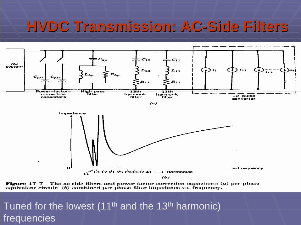
HVDC Transmission: ACHVDC Transmission: AC--Side FiltersSide Filters
Tuned for the lowest (11th and the 13th harmonic) frequencies

Effect of Reactive Power on Effect of Reactive Power on Voltage MagnitudeVoltage Magnitude
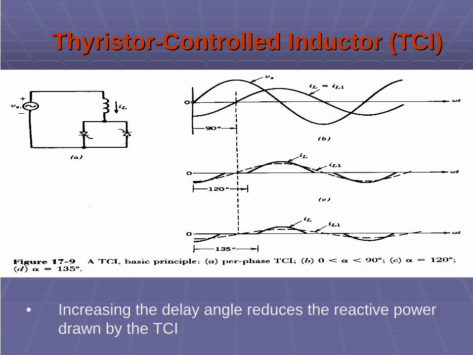
ThyristorThyristor--Controlled Inductor (TCI)Controlled Inductor (TCI)
• Increasing the delay angle reduces the reactive power drawn by the TCI

ThyristorThyristor--Switched Capacitors (Switched Capacitors (TSCsTSCs))
• Transient current at switching must be minimized
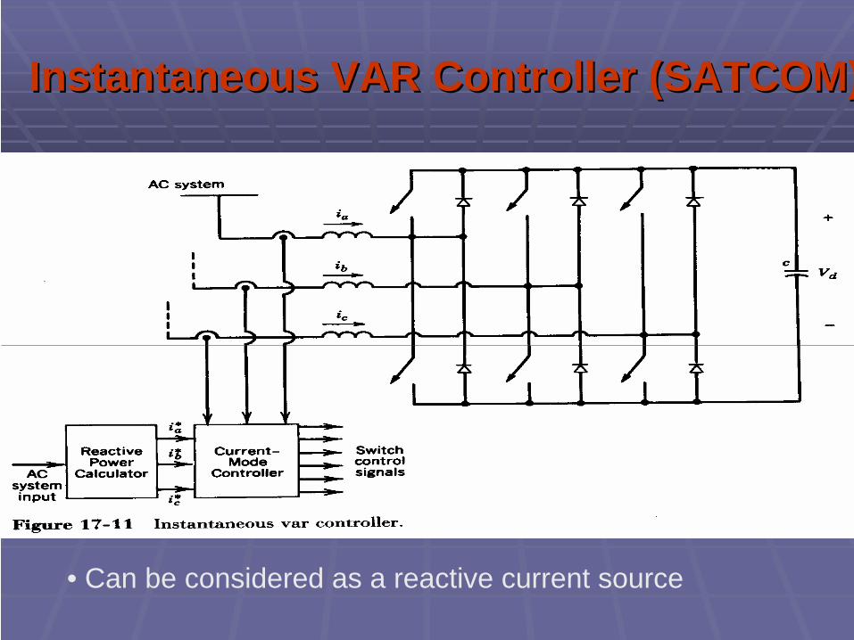
Instantaneous VAR Controller (SATCOM)Instantaneous VAR Controller (SATCOM)
• Can be considered as a reactive current source

Characteristics of Solar CellsCharacteristics of Solar Cells
• The maximum power point is at the knee of the characteristics

Photovoltaic InterfacePhotovoltaic Interface
• This scheme uses a thyristor inverter
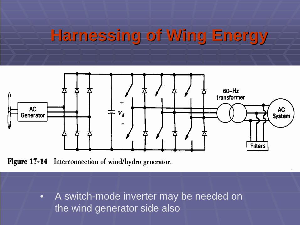
Harnessing of Wing EnergyHarnessing of Wing Energy
• A switch-mode inverter may be needed on the wind generator side also
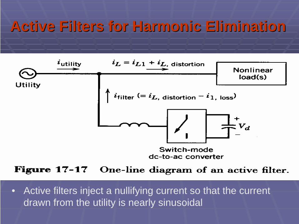
Active Filters for Harmonic EliminationActive Filters for Harmonic Elimination
• Active filters inject a nullifying current so that the current drawn from the utility is nearly sinusoidal
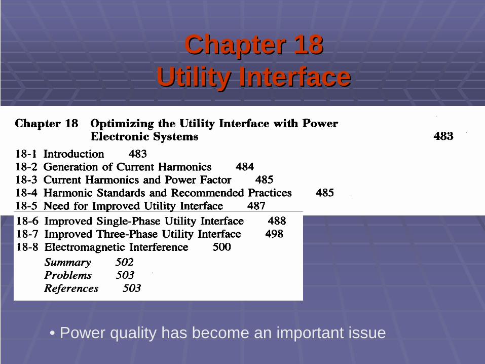
Chapter 18Chapter 18Utility InterfaceUtility Interface
• Power quality has become an important issue
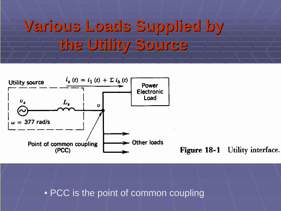
Various Loads Supplied by Various Loads Supplied by the Utility Sourcethe Utility Source
• PCC is the point of common coupling
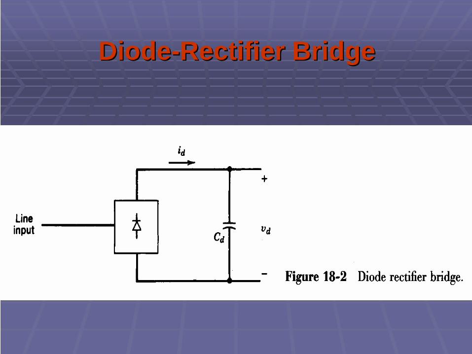
DiodeDiode--Rectifier BridgeRectifier Bridge

Typical Harmonics in the Input CurrentTypical Harmonics in the Input Current
• Single-phase diode-rectifier bridge

Harmonic Guidelines: IEEE 519Harmonic Guidelines: IEEE 519
• Commonly used for specifying limits on the input current distortion

Harmonic Guidelines: IEEE 519Harmonic Guidelines: IEEE 519
• Limits on distortion in the input voltage supplied by the utility

Reducing the Input Current DistortionReducing the Input Current Distortion
• use of passive filters
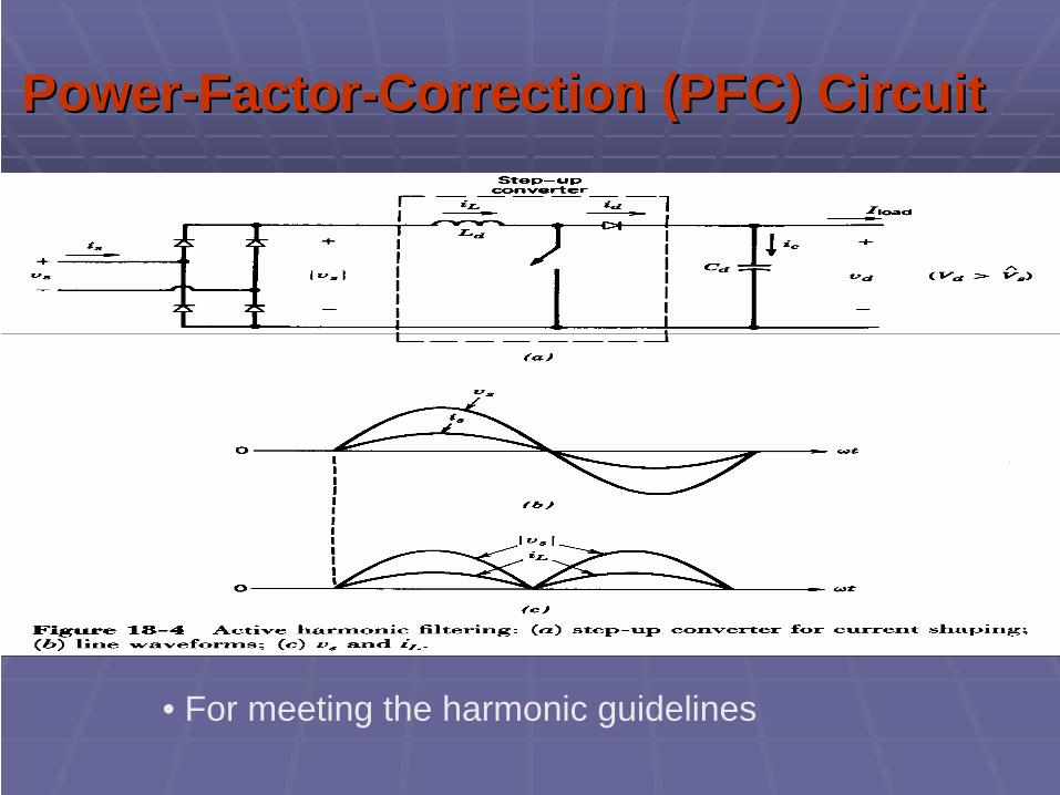
PowerPower--FactorFactor--Correction (PFC) CircuitCorrection (PFC) Circuit
• For meeting the harmonic guidelines
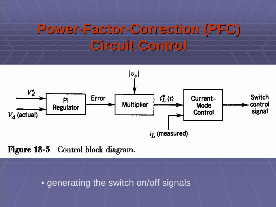
PowerPower--FactorFactor--Correction (PFC) Correction (PFC) Circuit ControlCircuit Control
• generating the switch on/off signals
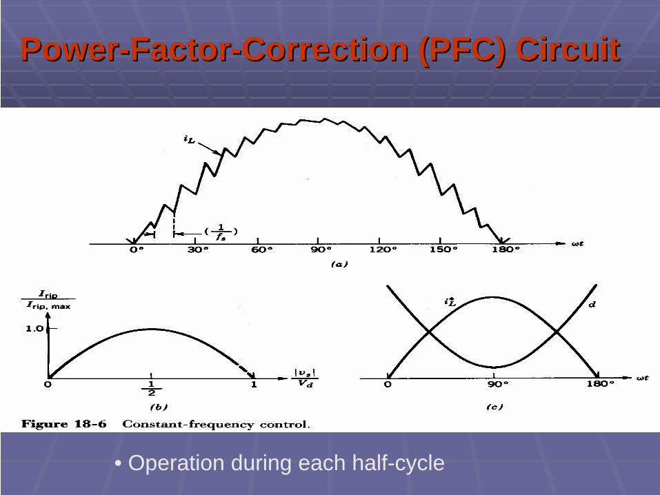
PowerPower--FactorFactor--Correction (PFC) CircuitCorrection (PFC) Circuit
• Operation during each half-cycle
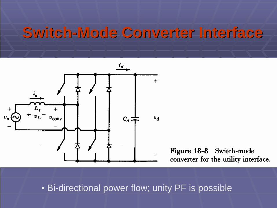
SwitchSwitch--Mode Converter InterfaceMode Converter Interface
• Bi-directional power flow; unity PF is possible

SwitchSwitch--Mode Converter ControlMode Converter Control
• DC bus voltage is maintained at the reference value

SwitchSwitch--Mode Converter InterfaceMode Converter Interface

EMI: Conducted EMI: Conducted InterefenceInterefence
• Common and differential modes

Switching WaveformsSwitching Waveforms
• Typical rise and fall times

Conducted EMIConducted EMI
• Various Standards

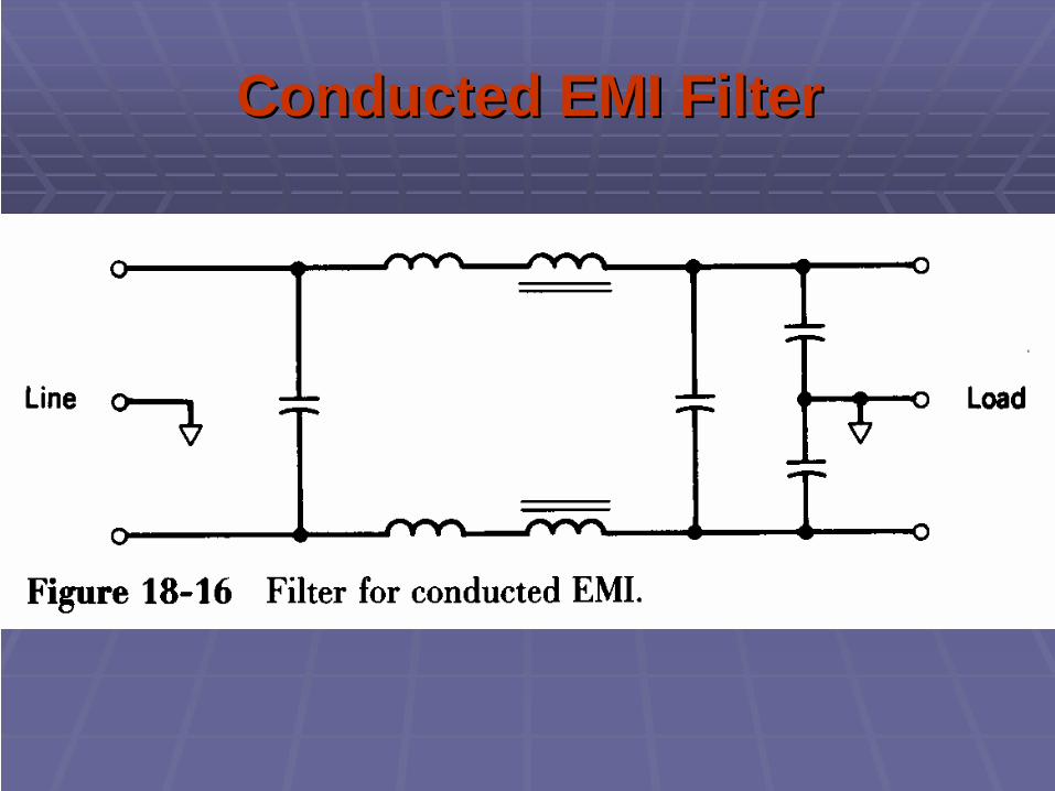
Conducted EMI FilterConducted EMI Filter

TurnTurn--off off SnubberSnubber
D f
D s
C s
R s
V d
I o+
-
i D F
i C s
Turn-off snubber
S w C s
I o - iV d
i sw
D fI o
sw
Cs=Iotfi2Vd
, ton>2.3RsCs, Vd/Rs<0.2Io
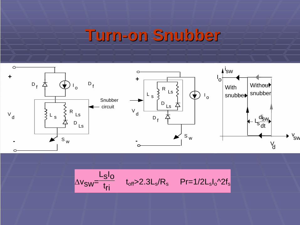
TurnTurn--on on SnubberSnubber
V d
+
-
L sD Ls
D f
R Ls
I o
S w
V d
-
L sD Ls
D f R Ls I o
S w
D f
+
Snubber circuit
swi
vswVd
Io
Lsdiswdt
Without snubber
With snubber
Δvsw=LsIotri
toff>2.3Ls/Rs Pr=1/2LsIo^2fs

Aspects of EMC (EMIAspects of EMC (EMI、、EMS)EMS)
EMCEMC is concerned with the generation, is concerned with the generation, transmission, and reception of transmission, and reception of electromagnetic energyelectromagnetic energyEMIEMI occurs if the received energy occurs if the received energy causes the receptor to behave in an causes the receptor to behave in an undesired mannerundesired manner

EMI Sources and SensorsEMI Sources and Sensors

Three Ways to Prevent Interference
Suppress the emission at its source
Make the coupling path as inefficient as possible
Make the receptor less susceptible to the emission
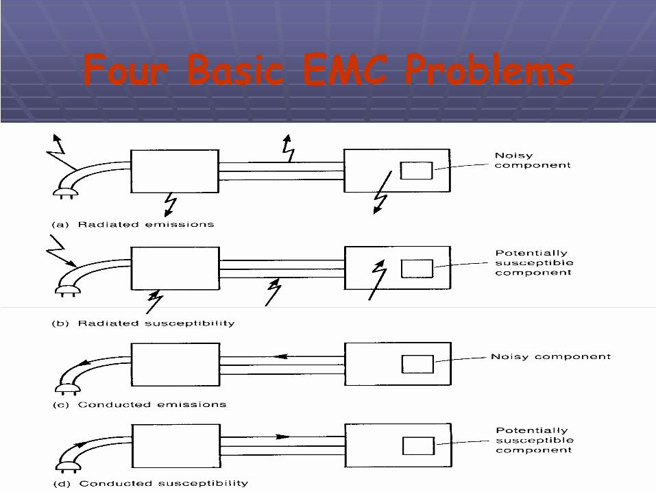
Four Basic EMC Problems
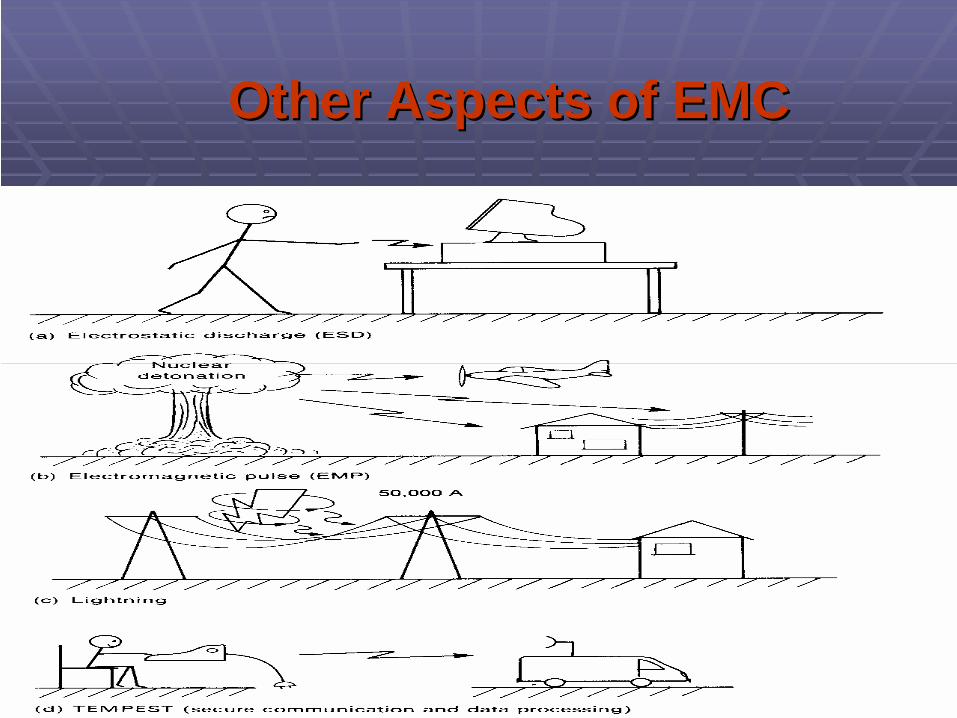
Other Aspects of EMCOther Aspects of EMC
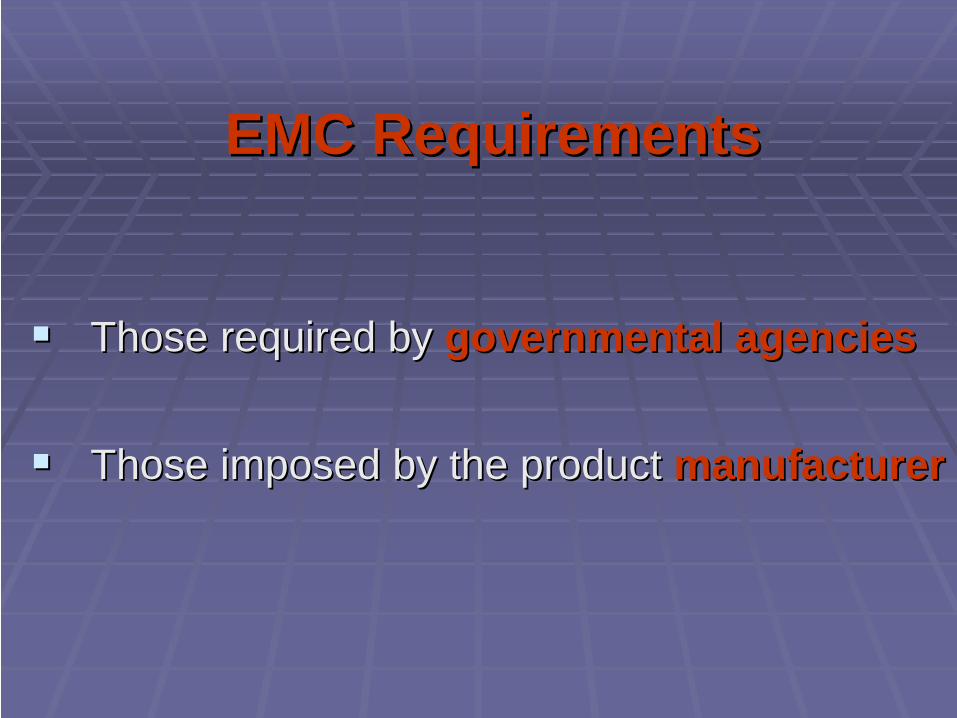
EMC RequirementsEMC Requirements
Those required by Those required by governmental agenciesgovernmental agencies
Those imposed by the product Those imposed by the product manufacturermanufacturer

Frequency Range of EMC Requirements
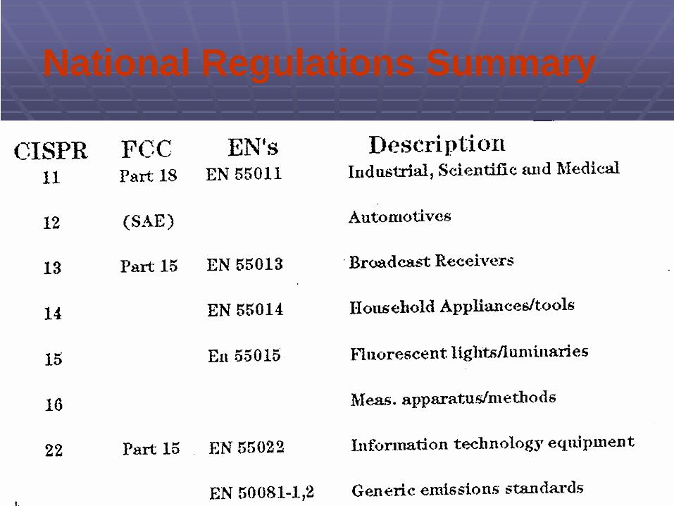
National Regulations Summary
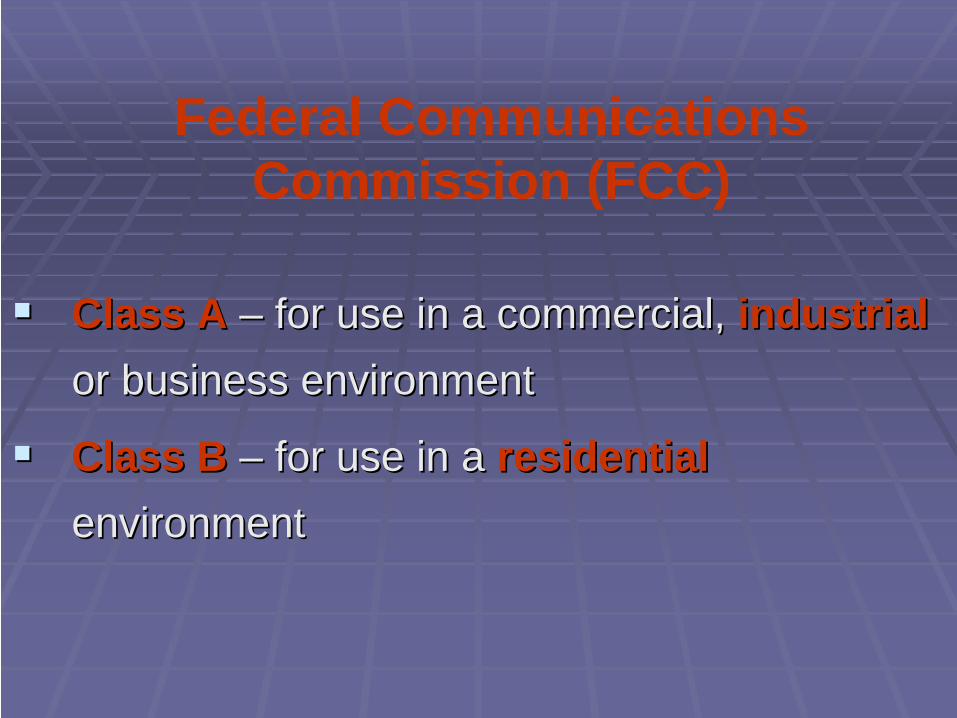
Federal Communications Commission (FCC)
Class AClass A –– for use in a commercial, for use in a commercial, industrialindustrialor business environmentor business environment
Class BClass B –– for use in a for use in a residential residential environmentenvironment

FCC Emission for Class B
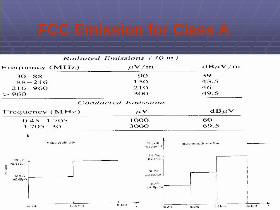
FCC Emission for Class A
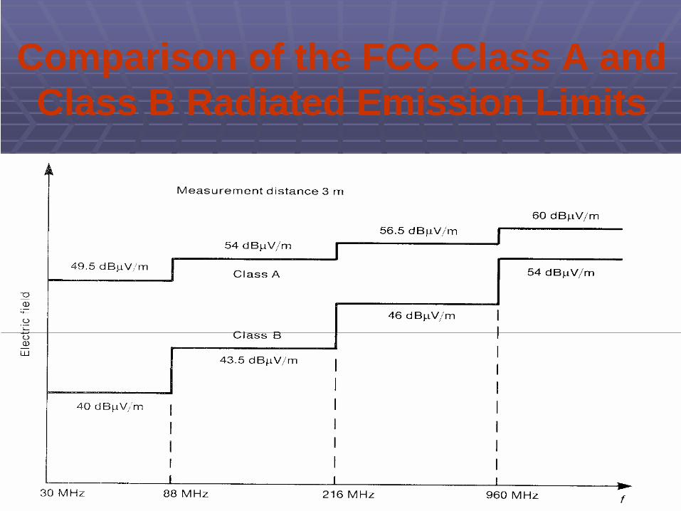
Comparison of the FCC Class A and Class B Radiated Emission Limits
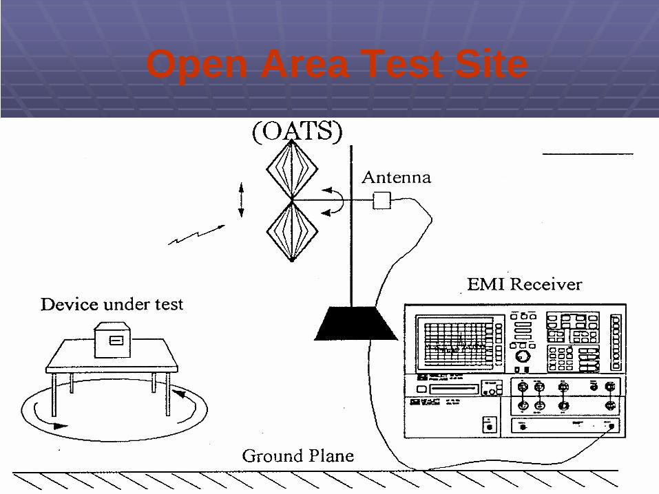
Open Area Test Site
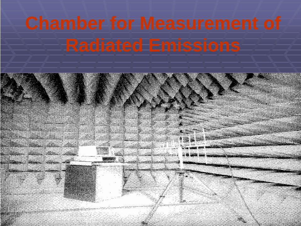
Chamber for Measurement of Radiated Emissions
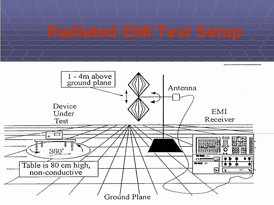
Radiated EMI Test Setup
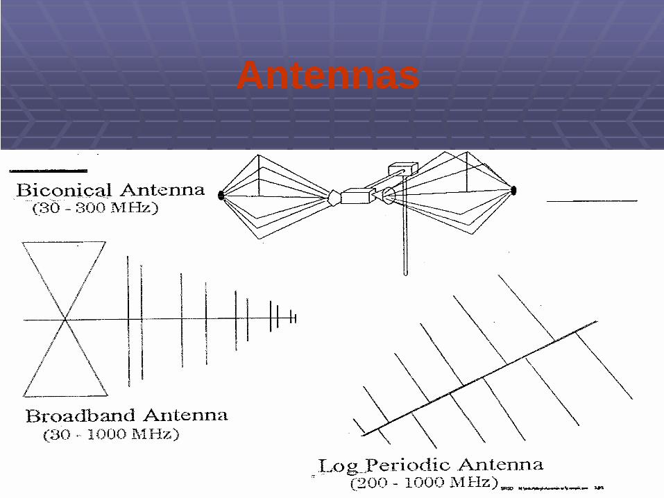
Antennas

Conducted EMI Test Setup
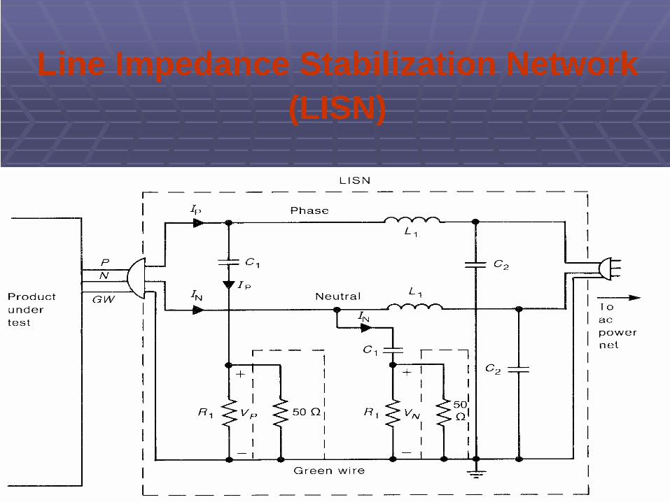
Line Impedance Stabilization Network (LISN)
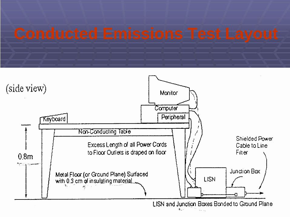
Conducted Emissions Test Layout

Conducted Emissions Test Layout
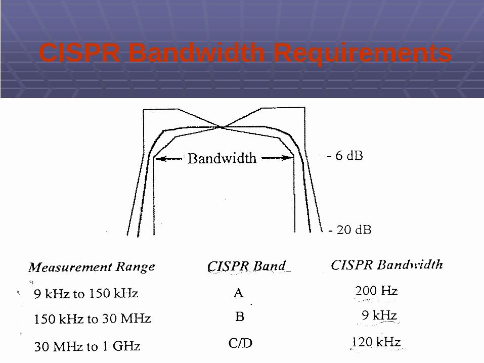
CISPR Bandwidth Requirements
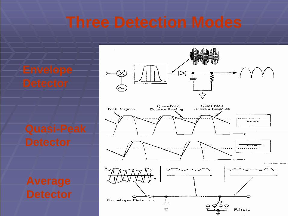
Three Detection Modes
Envelope Detector
Quasi-Peak Detector
Average Detector
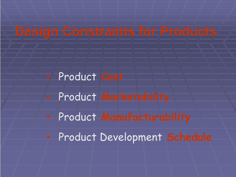
Design Constraints for Products
Product Cost
Product Marketability
Product Manufacturability
Product Development Schedule
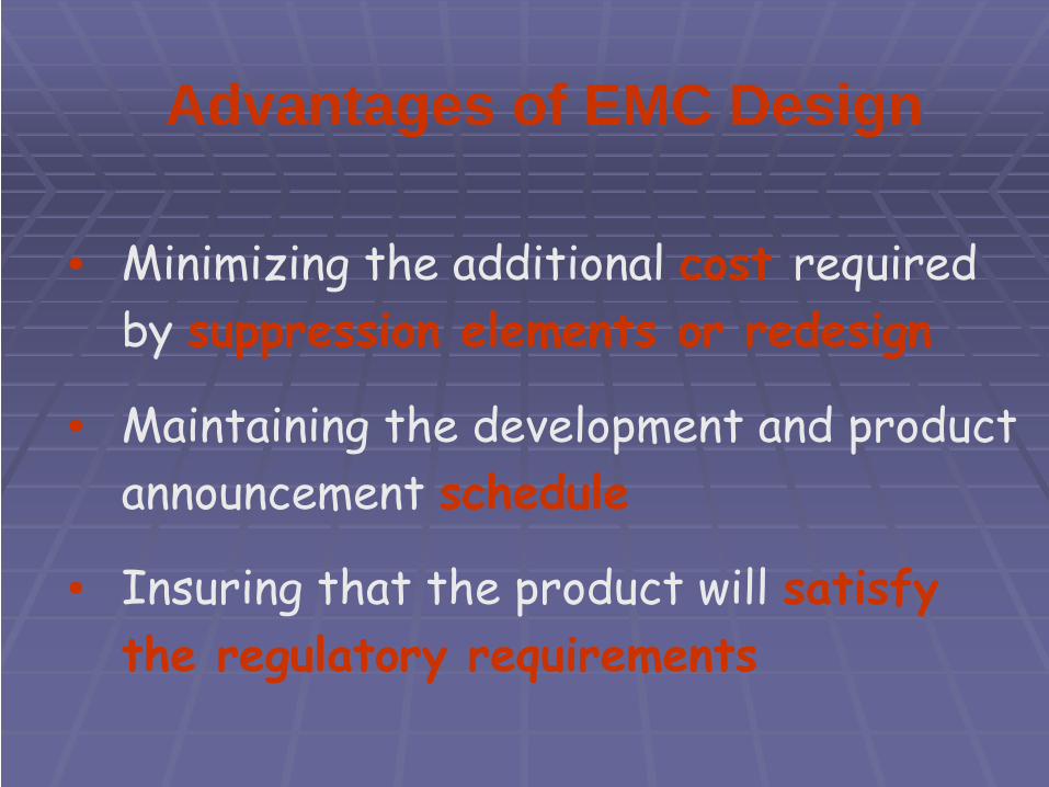
Advantages of EMC Design
Minimizing the additional cost required by suppression elements or redesign
Maintaining the development and product announcement schedule
Insuring that the product will satisfy the regulatory requirements

Effects of Component Leads

Resistors
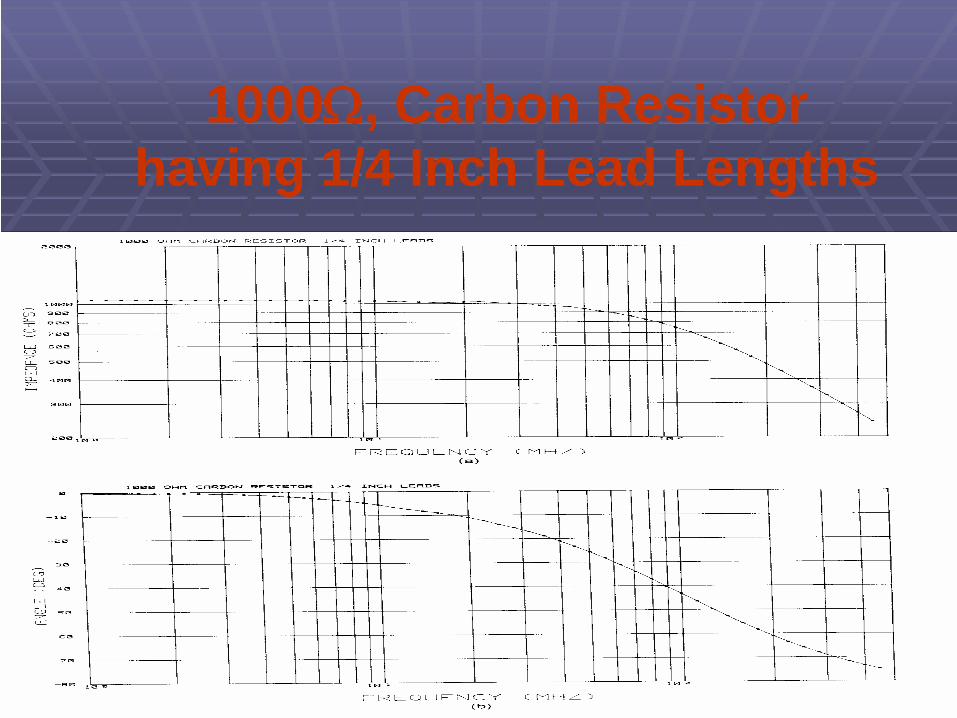
1000Ω, Carbon Resistor having 1/4 Inch Lead Lengths
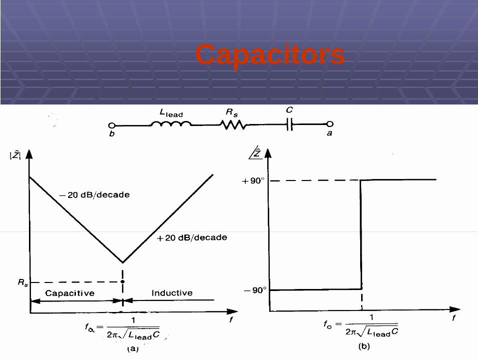
Capacitors
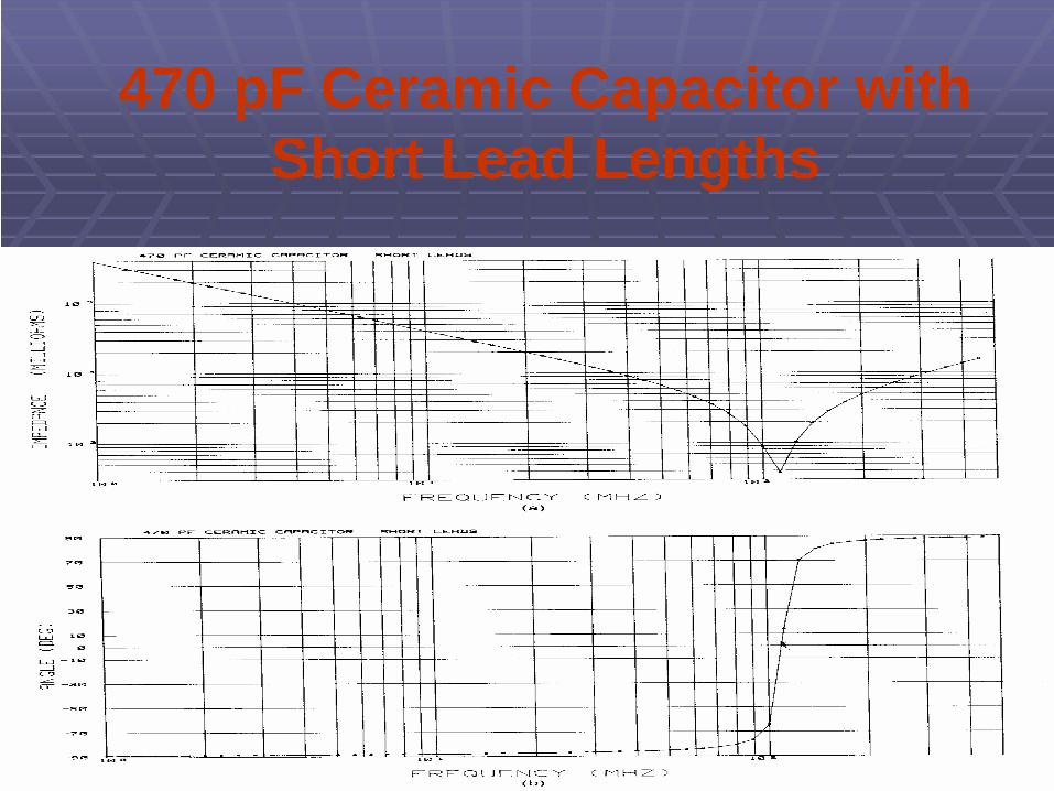
470 pF Ceramic Capacitor with Short Lead Lengths
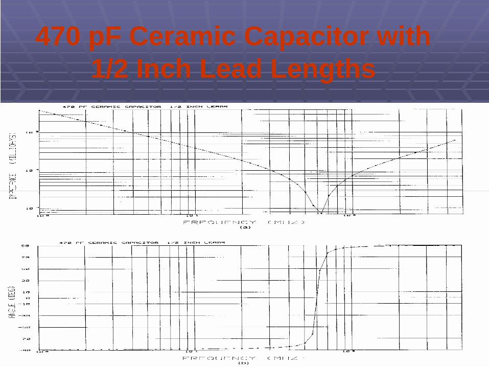
470 pF Ceramic Capacitor with 1/2 Inch Lead Lengths
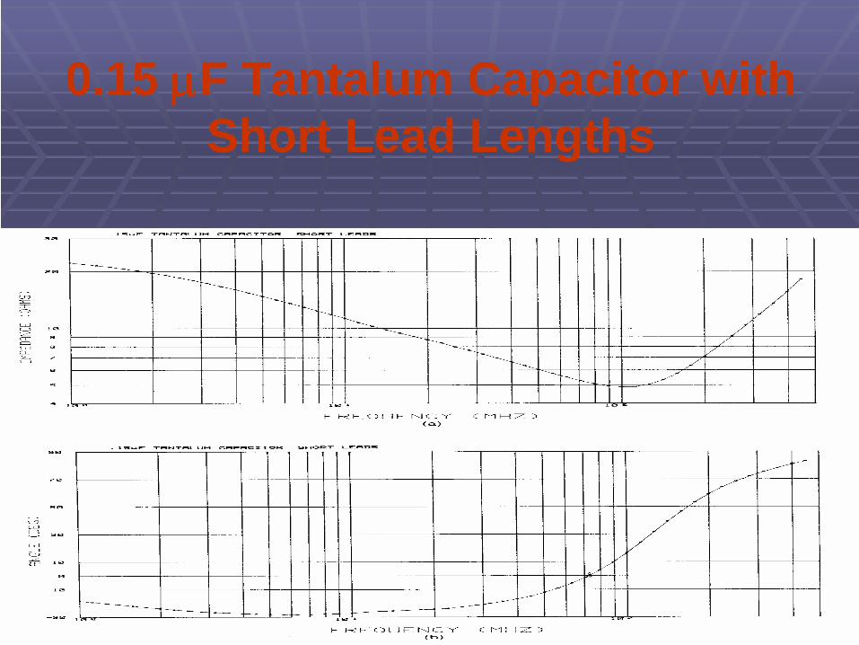
0.15 μF Tantalum Capacitor with Short Lead Lengths

0.15 μF Tantalum Capacitor with 1/2 Inch Lead Lengths

Inductors
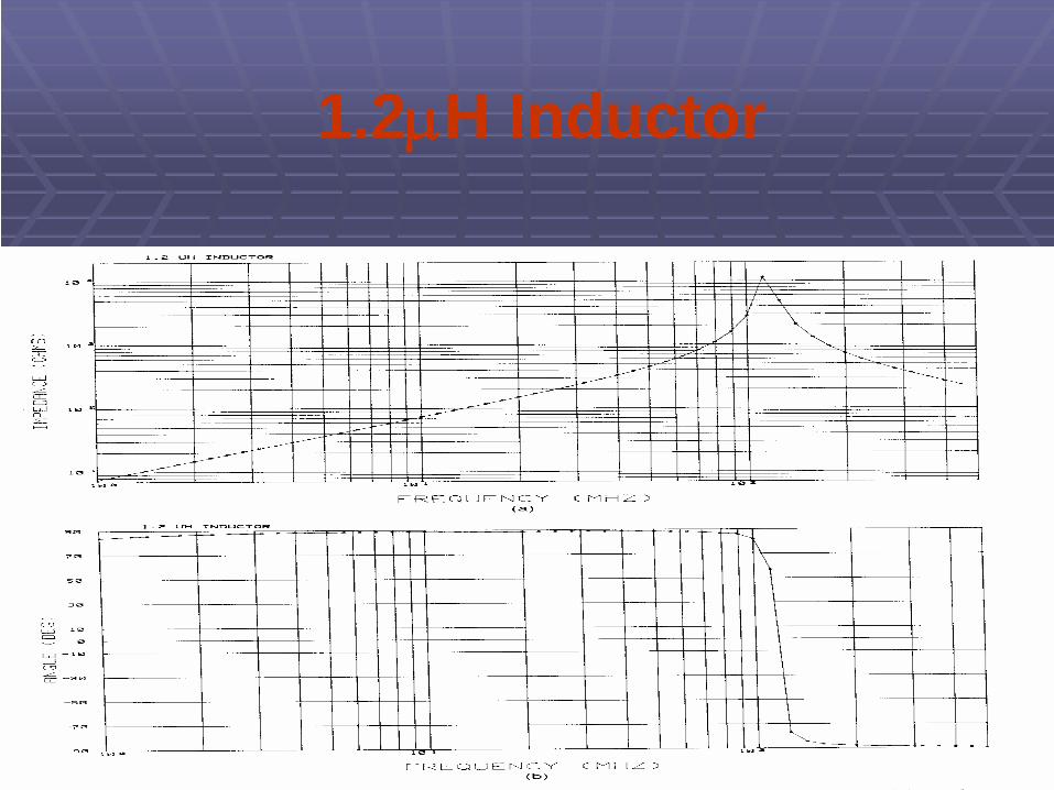
1.2μH Inductor

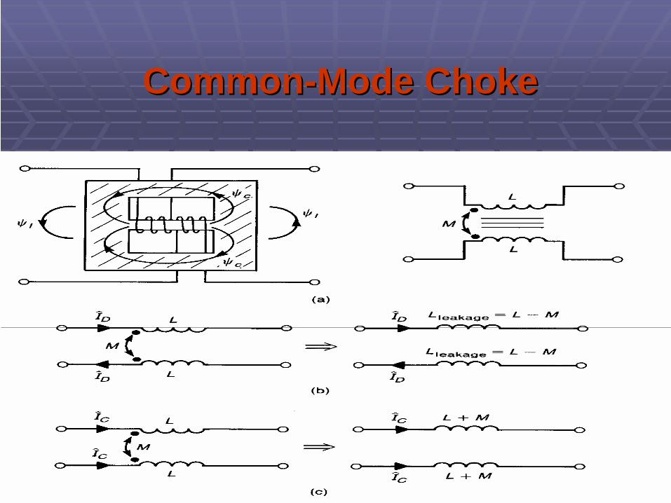
CommonCommon--Mode ChokeMode Choke
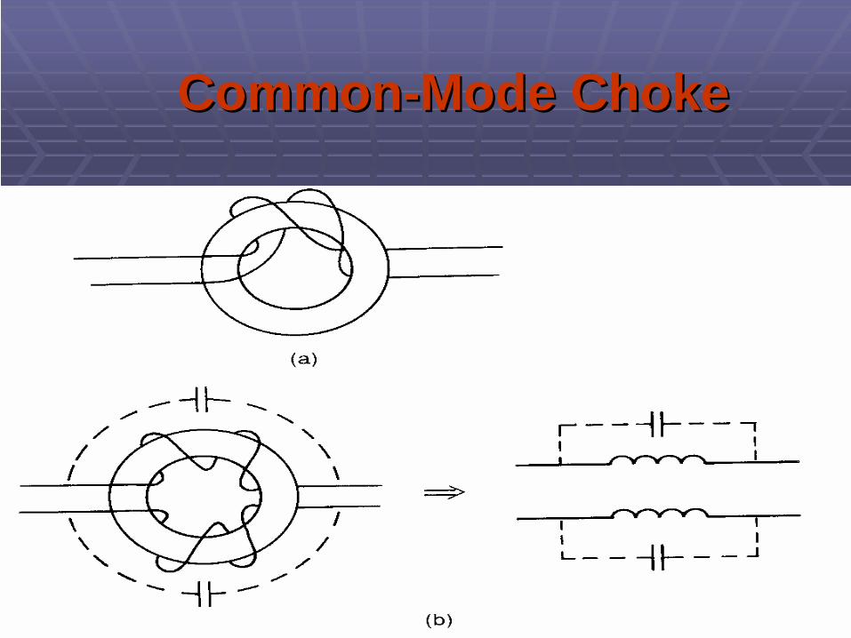
CommonCommon--Mode ChokeMode Choke

Frequency Response of the Frequency Response of the Relative Relative PermeabilitiesPermeabilities of Ferriteof Ferrite
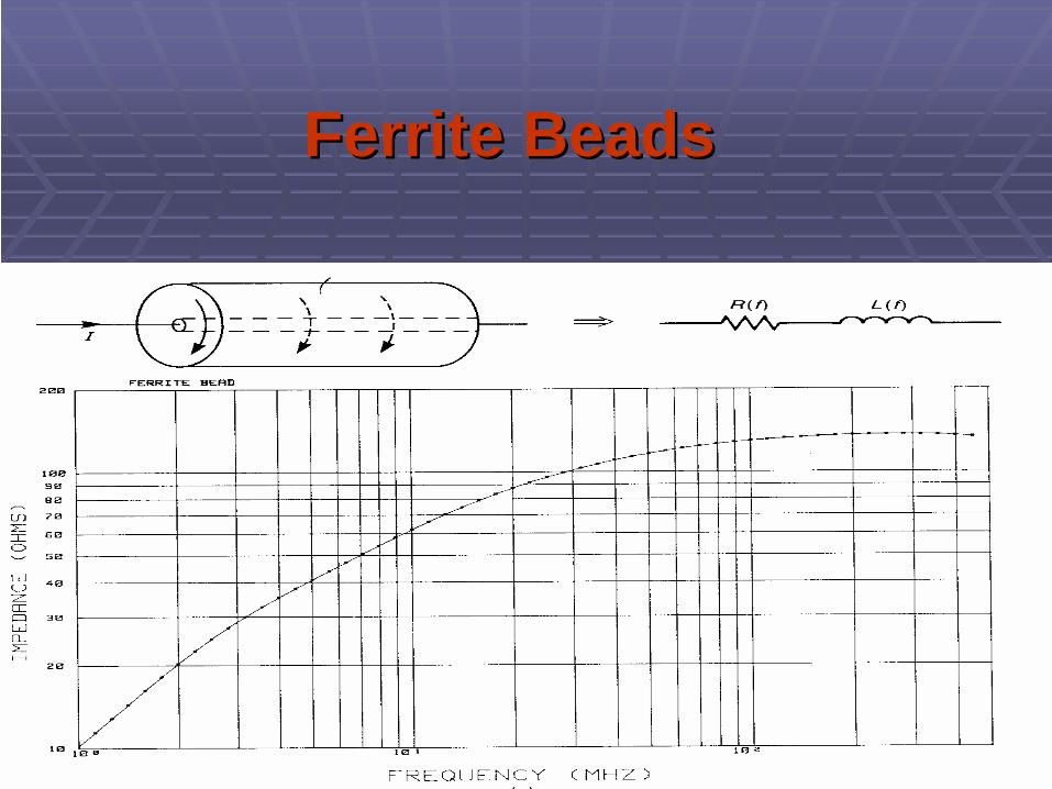
Ferrite BeadsFerrite Beads

MultiMulti--Turn Ferrite BeadsTurn Ferrite Beads
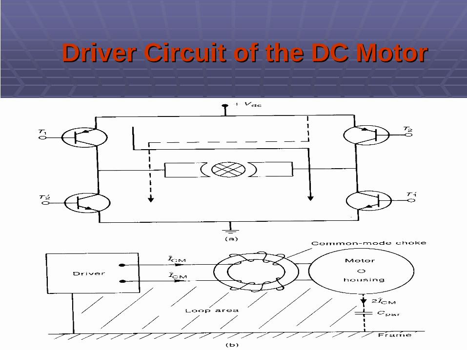
Driver Circuit of the DC MotorDriver Circuit of the DC Motor
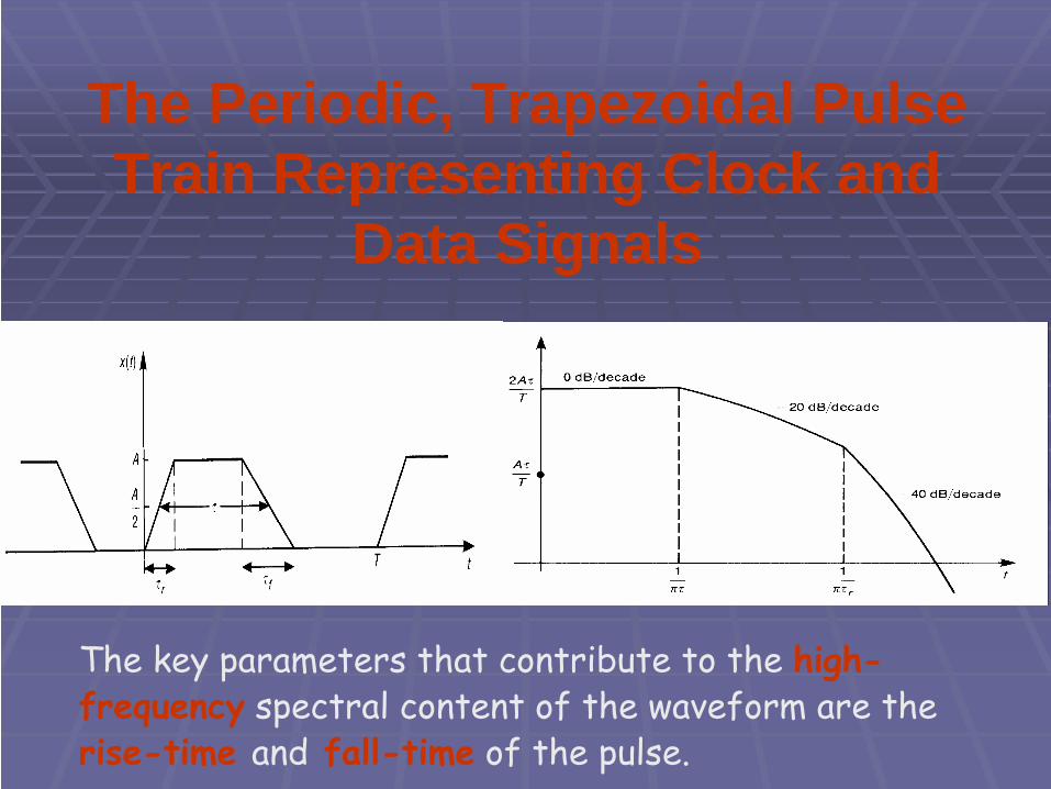
The Periodic, Trapezoidal Pulse Train Representing Clock and
Data Signals
The key parameters that contribute to the high- frequency
spectral content of the waveform are the
rise-time and
fall-time
of the pulse.
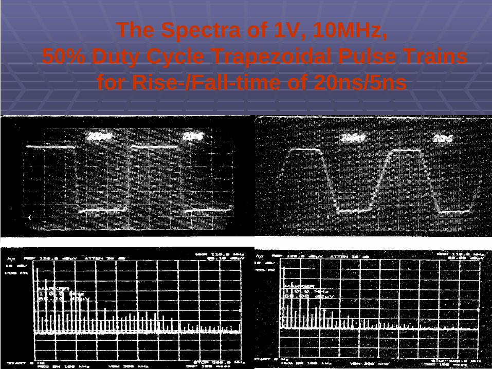
The Spectra of 1V, 10MHz,50% Duty Cycle Trapezoidal Pulse Trains
for Rise-/Fall-time of 20ns/5ns
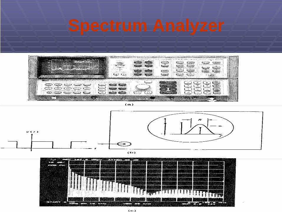
Spectrum Analyzer
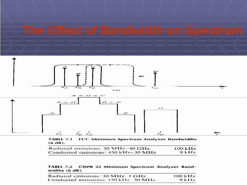
The Effect of Bandwidth on Spectrum

The Effects of Differential-Mode Current and Common-Mode Currents
Common-mode current often produce larger radiated emissions than the differential-mode currents
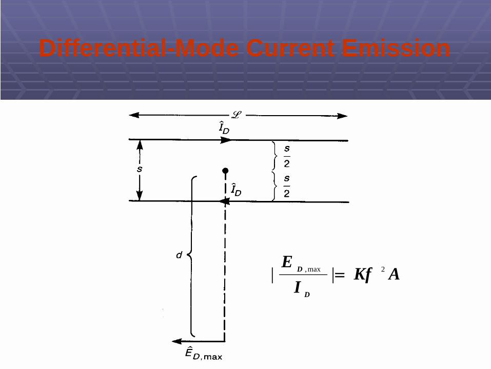
Differential-Mode Current Emission
AKfI
E
D
D 2max, || =
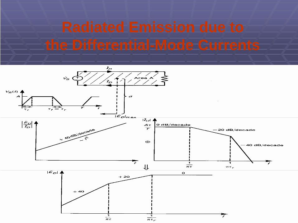
Radiated Emission due to the Differential-Mode Currents
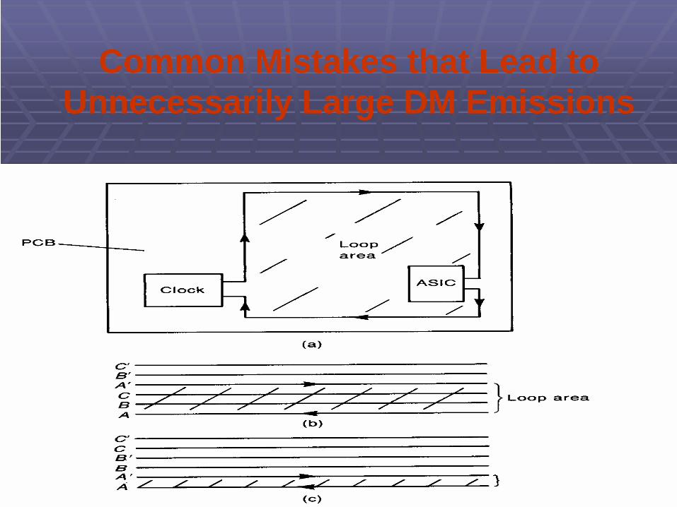
Common Mistakes that Lead to Unnecessarily Large DM Emissions

Common-Mode Current Emission
LKfI
E
C
C =|| max,
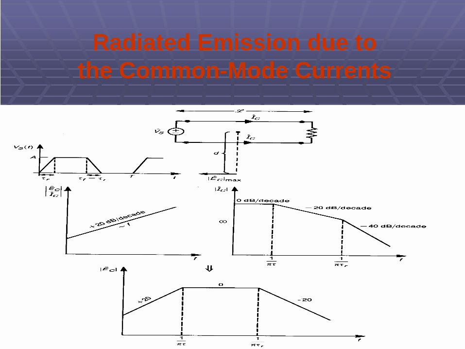
Radiated Emission due to the Common-Mode Currents

Susceptibility Models

10V/m, 100MHz Incident Uniform Plane Wave

Measurement of Conducted Emissions

Line Impedance Stabilization Network (LISN)
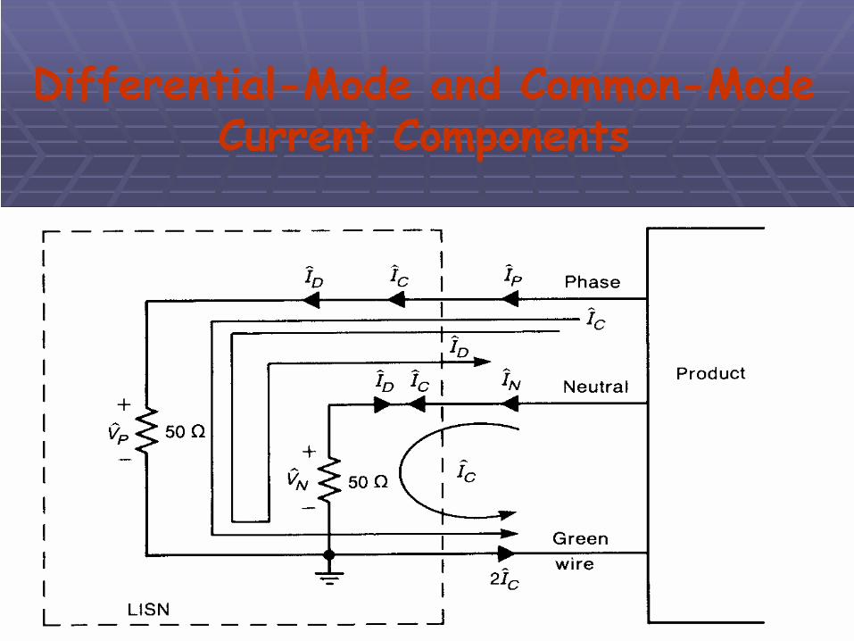
Differential-Mode and Common-Mode Current Components

Methods of Reducing the Common-Mode Conducted Emissions

Definition of the Insertion Loss of a Filter
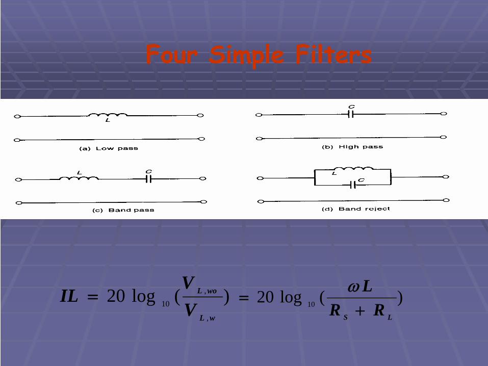
Four Simple Filters
)(log20,
,10
wL
woL
VV
IL = )(log20 10
LS RRL+
=ω
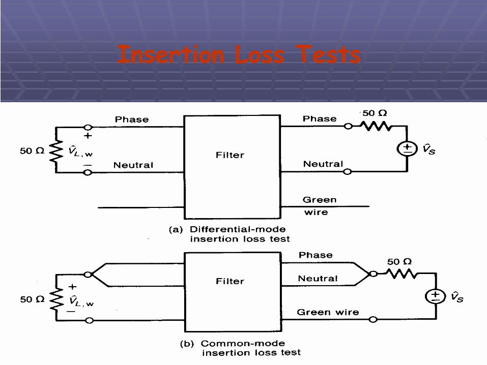
Insertion Loss Tests
Conducted EMI FilterConducted EMI Filter
CommonCommon--Mode ChokeMode Choke

The Equivalent Circuit of the FilterThe Equivalent Circuit of the Filterfor Commonfor Common--Mode CurrentsMode Currents
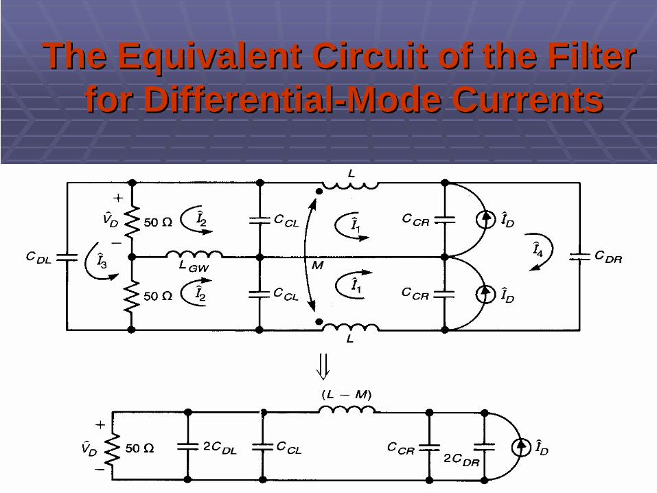
The Equivalent Circuit of the FilterThe Equivalent Circuit of the Filterfor Differentialfor Differential--Mode CurrentsMode Currents
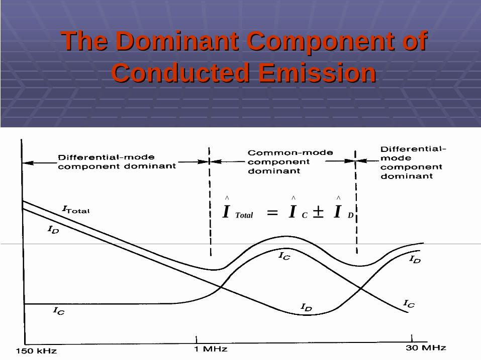
The Dominant Component of The Dominant Component of Conducted EmissionConducted Emission
DCTotal III^^^
±=
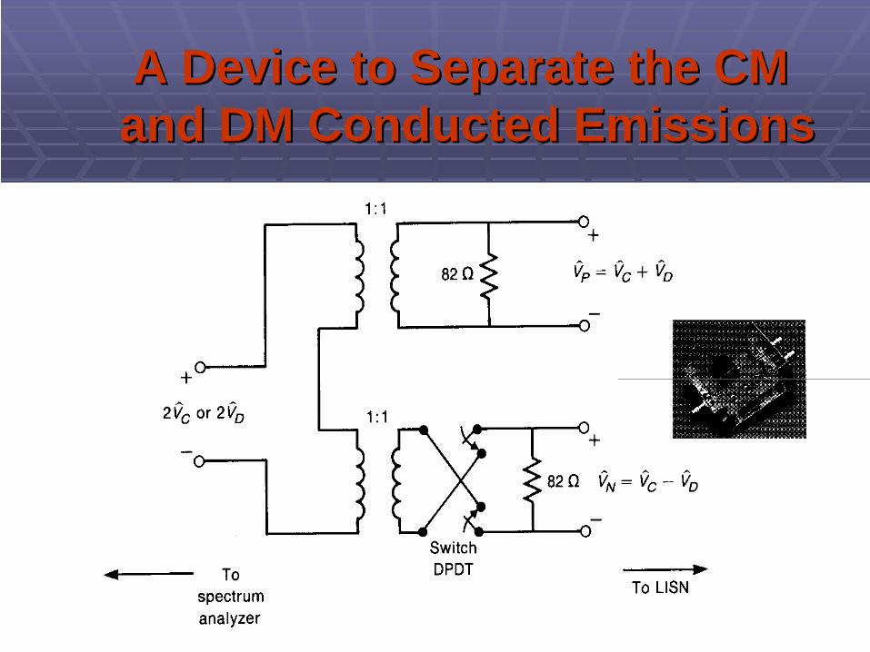
A Device to Separate the CMA Device to Separate the CMand DM Conducted Emissionsand DM Conducted Emissions
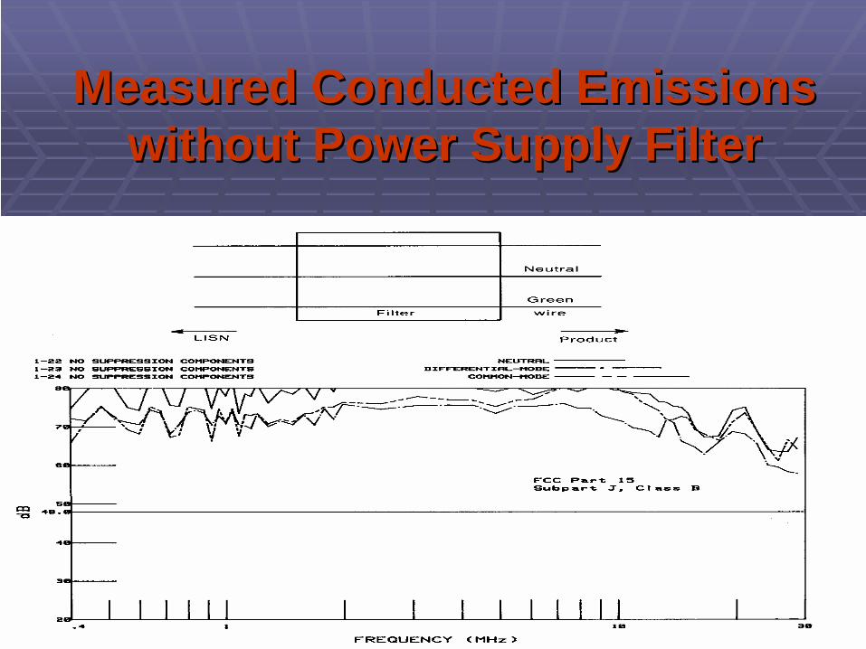
Measured Conducted Emissions Measured Conducted Emissions without Power Supply Filterwithout Power Supply Filter

Measured Conducted Emissions Measured Conducted Emissions with 3300with 3300pF LinepF Line--toto--Ground Cap. Ground Cap.
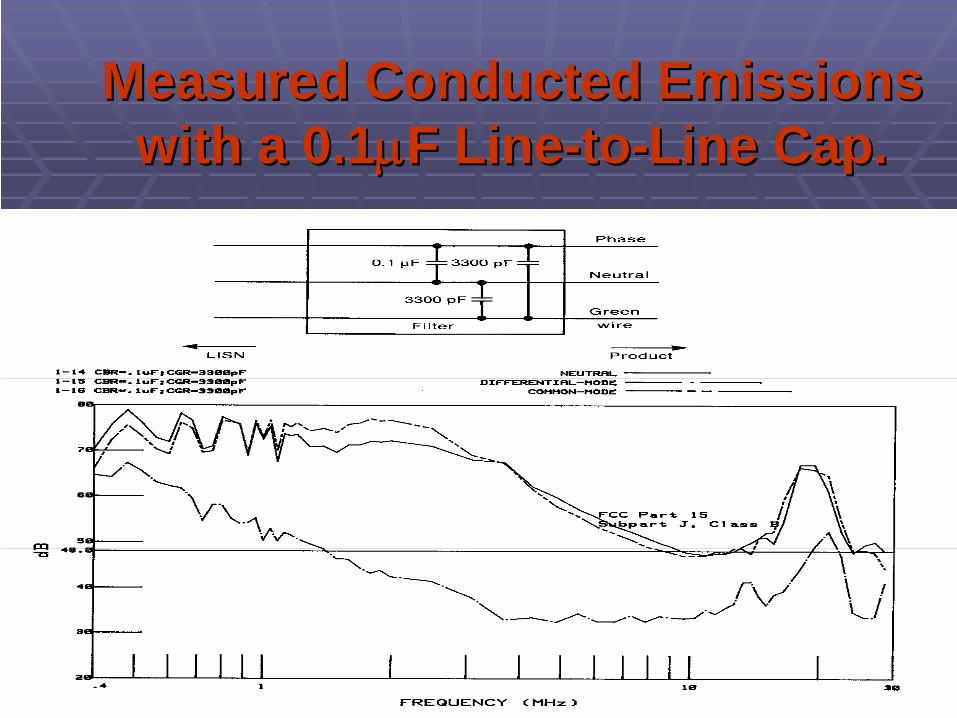
Measured Conducted Emissions Measured Conducted Emissions with a 0.1with a 0.1μμF LineF Line--toto--Line Cap. Line Cap.

Measured Conducted Emissions Measured Conducted Emissions with a Green Wire Inductorwith a Green Wire Inductor
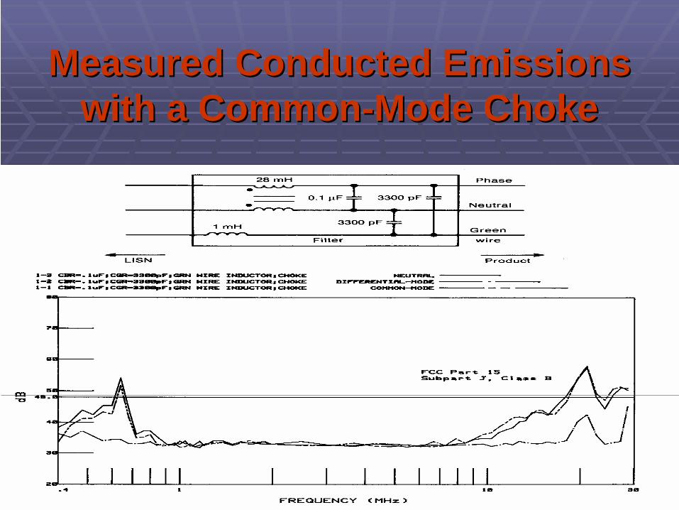
Measured Conducted Emissions Measured Conducted Emissions with a Commonwith a Common--Mode ChokeMode Choke

NonidealNonideal Effects in DiodesEffects in Diodes

Construction of TransformersConstruction of Transformers
The Effect of PrimaryThe Effect of Primary--toto--Secondary Secondary Capacitance of a TransformerCapacitance of a Transformer

The Proper Filter Placement in the The Proper Filter Placement in the Reduction of Conducted EmissionsReduction of Conducted Emissions

The unintended EM coupling between wires and
PCB lands that are in close proximity.
Crosstalk between wires in cables or between lands
on PCBs concerns the intrasystem interference
performance of the product.
CrosstalkCrosstalk
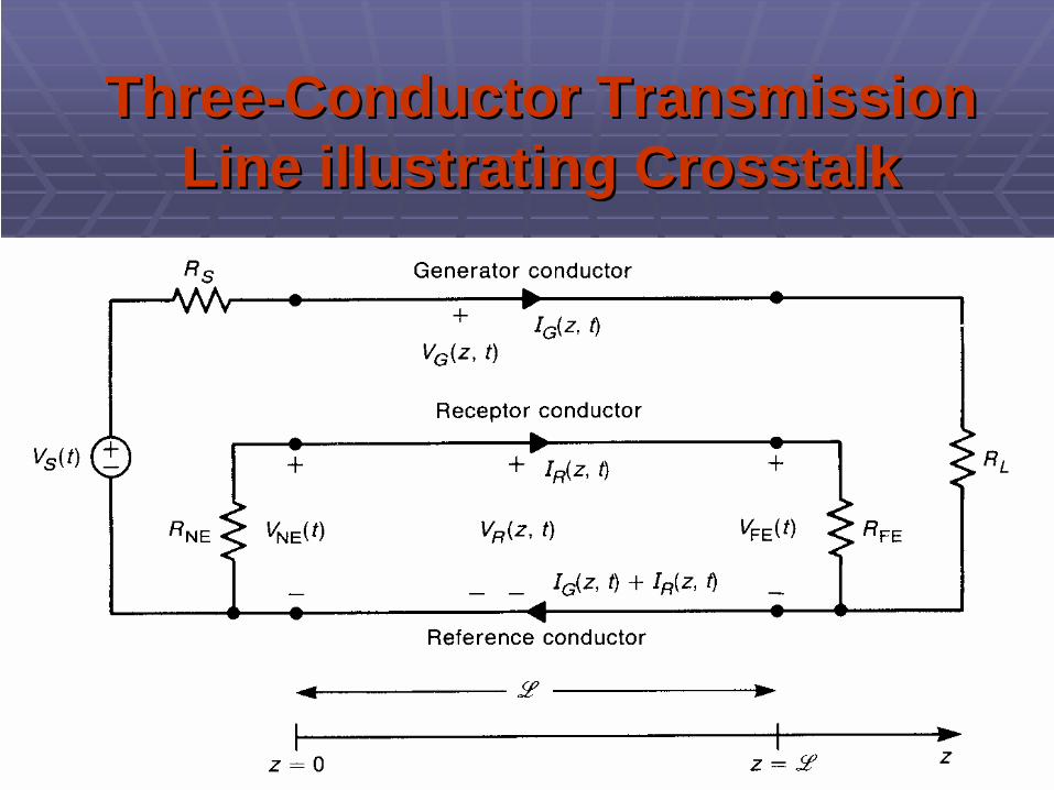
ThreeThree--Conductor Transmission Conductor Transmission Line illustrating CrosstalkLine illustrating Crosstalk
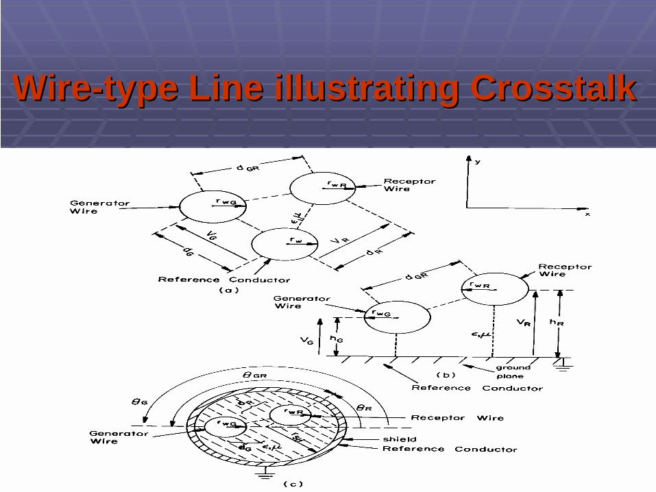
WireWire--type Line illustrating Crosstalktype Line illustrating Crosstalk
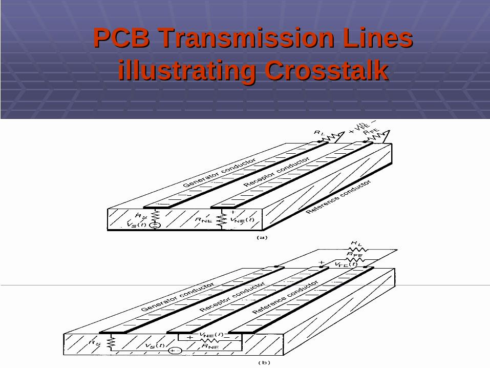
PCB Transmission Lines PCB Transmission Lines illustrating Crosstalkillustrating Crosstalk
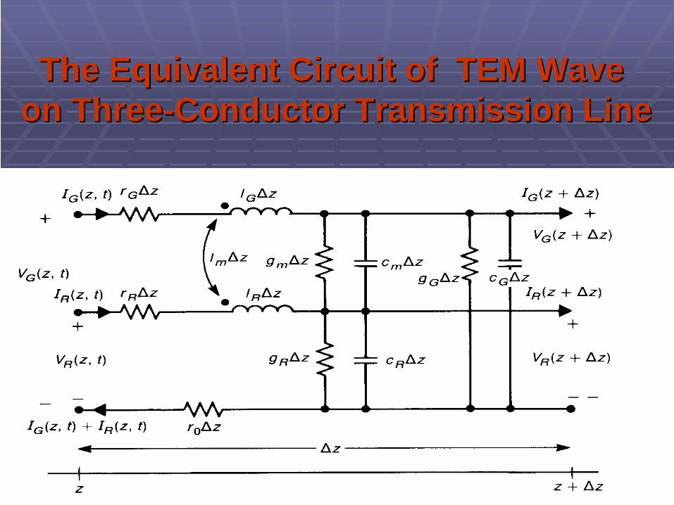
The Equivalent Circuit of TEM WaveThe Equivalent Circuit of TEM Waveon Threeon Three--Conductor Transmission LineConductor Transmission Line

The Simple InductiveThe Simple Inductive--Capacitive Capacitive Coupling ModelCoupling Model
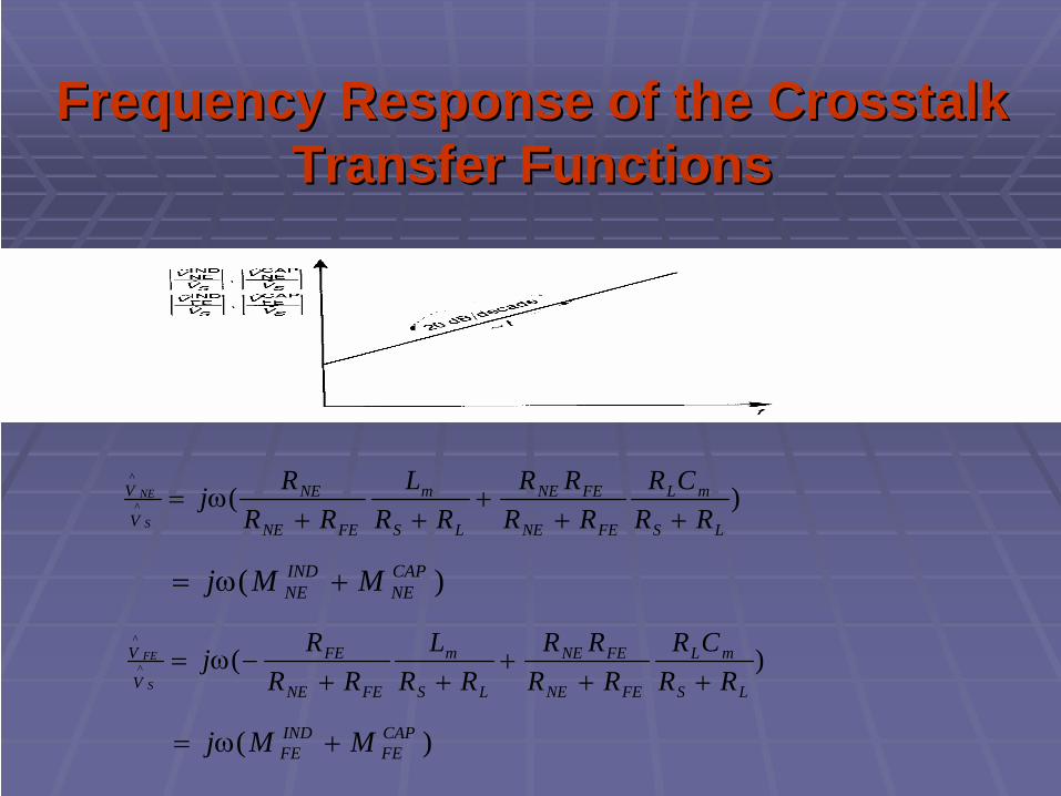
Frequency Response of the Crosstalk Frequency Response of the Crosstalk Transfer FunctionsTransfer Functions
)(^
^
LS
mL
FENE
FENE
LS
m
FENE
NE
V
V
RRCR
RRRR
RRL
RRRj
S
NE
+++
++ω=
)( CAPNE
INDNE MMj +ω=
)(^
^
LS
mL
FENE
FENE
LS
m
FENE
FE
V
V
RRCR
RRRR
RRL
RRRj
S
FE
+++
++−ω=
)( CAPFE
INDFE MMj +ω=
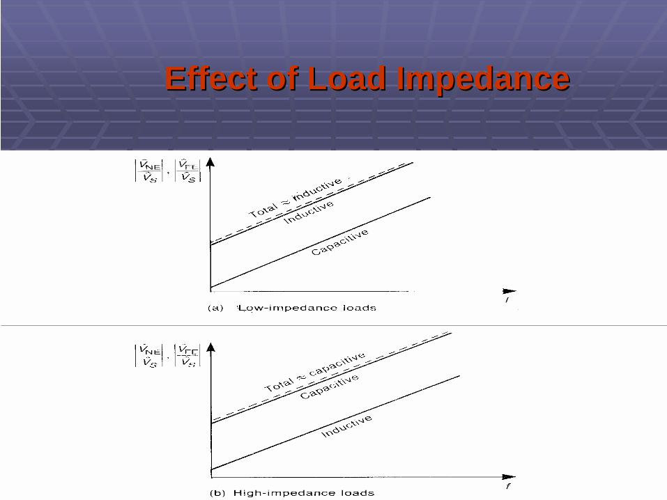
Effect of Load ImpedanceEffect of Load Impedance
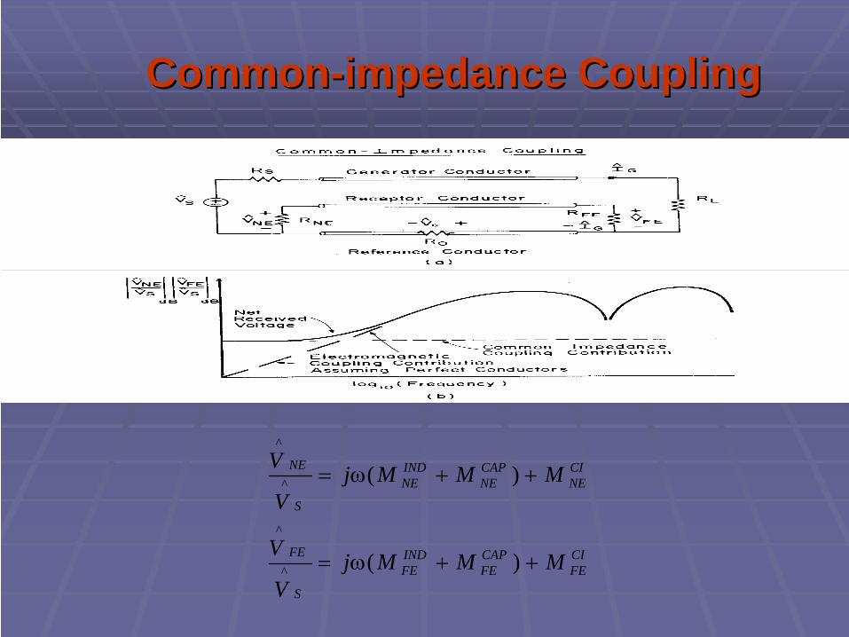
CommonCommon--impedance Couplingimpedance Coupling
CINE
CAPNE
INDNE
S
NE MMMjV
V++ω= )(^
^
CIFE
CAPFE
INDFE
S
FE MMMjV
V++ω= )(^
^

TimeTime--Domain Crosstalk for R=50Domain Crosstalk for R=50ΩΩ
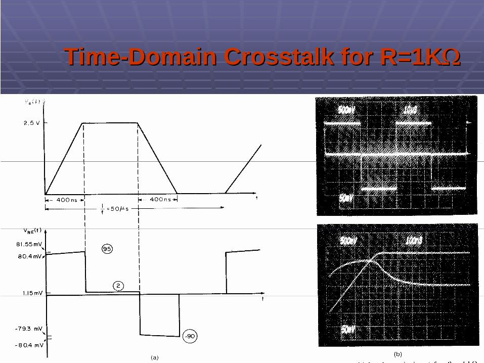
TimeTime--Domain Crosstalk for R=1KDomain Crosstalk for R=1KΩΩ
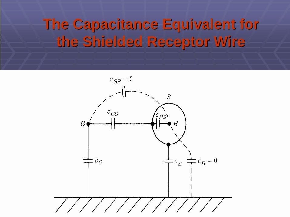
The Capacitance Equivalent for The Capacitance Equivalent for the Shielded Receptor Wirethe Shielded Receptor Wire

The Lumped Equivalent Circuit for The Lumped Equivalent Circuit for Capacitive CouplingCapacitive Coupling
CAP
FE
CAP
NE VV^^
= DCGGSRS
GSRS
FENE
FENE VCC
CCRR
RRj++
ω≅
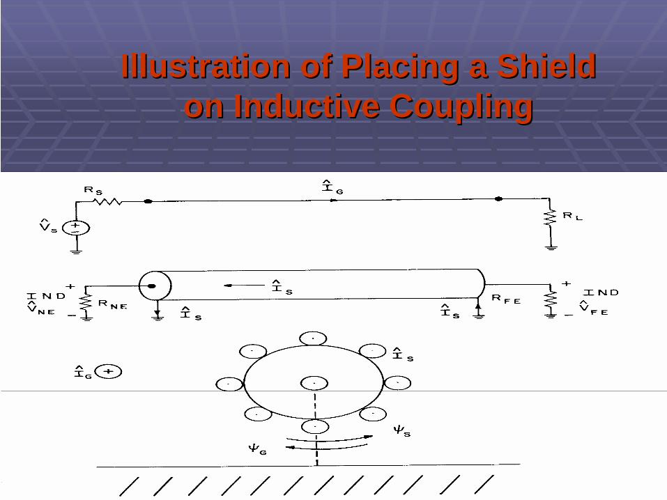
Illustration of Placing a Shield Illustration of Placing a Shield on Inductive Couplingon Inductive Coupling
SHSH
SHGGR
FENE
NEIND
NELjR
RILjRR
RVω+
ω+
=^^
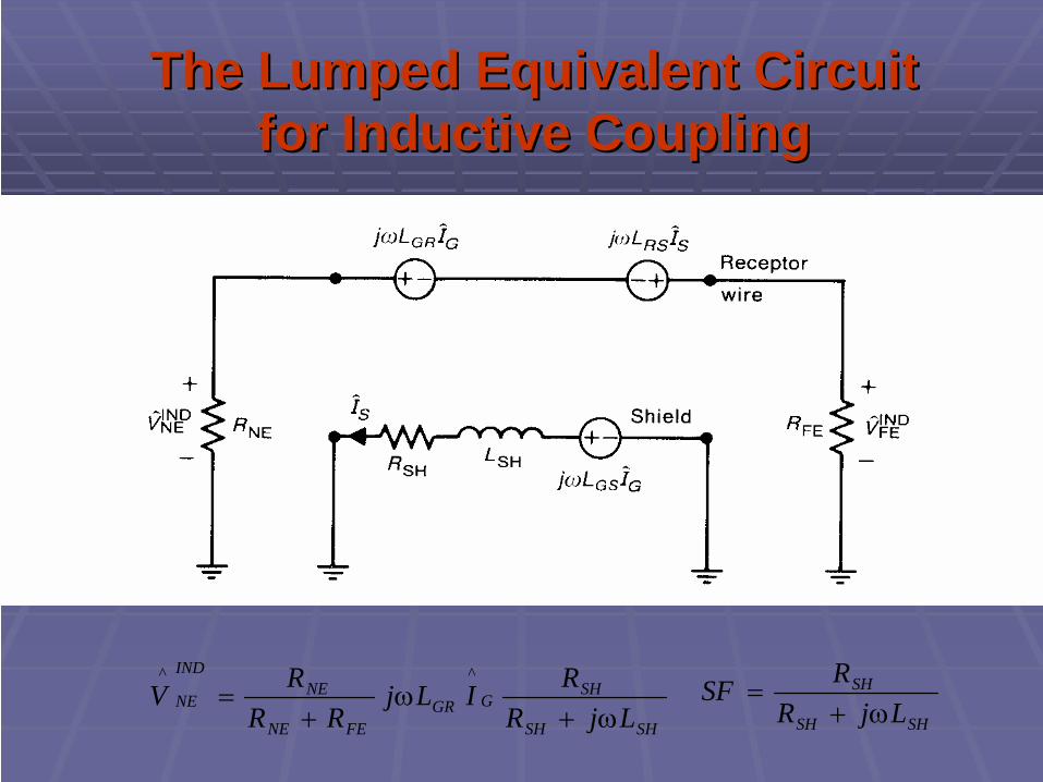
The Lumped Equivalent Circuit The Lumped Equivalent Circuit for Inductive Couplingfor Inductive Coupling
SHSH
SH
LjRRSF
ω+=
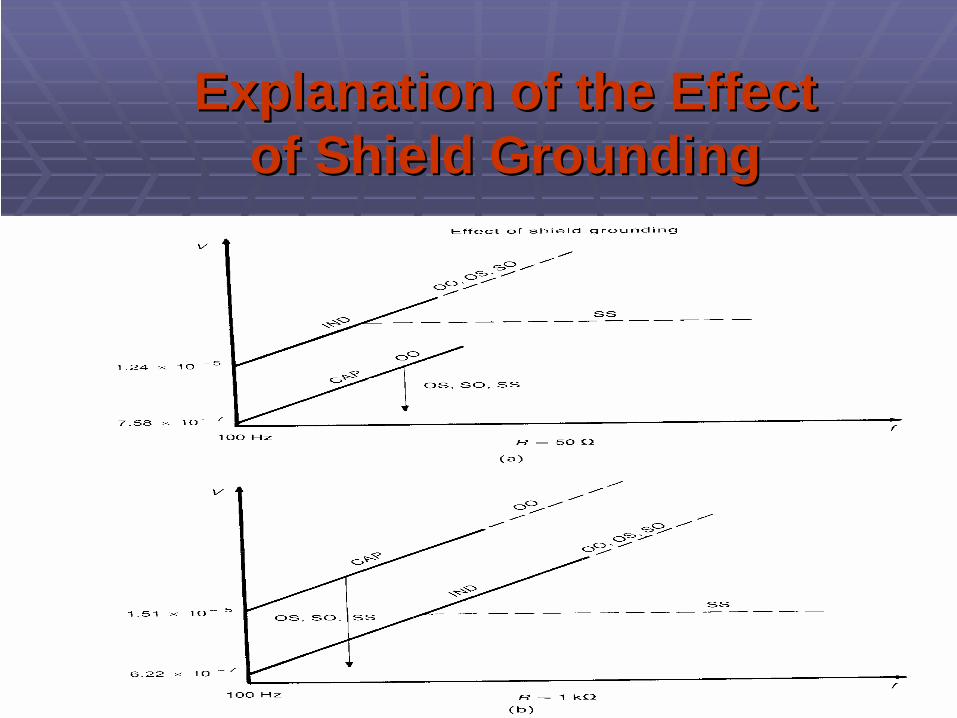
Explanation of the EffectExplanation of the Effectof Shield Groundingof Shield Grounding

Twisted WiresTwisted Wires

The InductiveThe Inductive--Capacitive Capacitive Coupling ModelCoupling Model
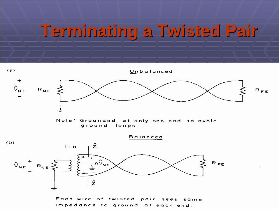
Terminating a Twisted PairTerminating a Twisted Pair
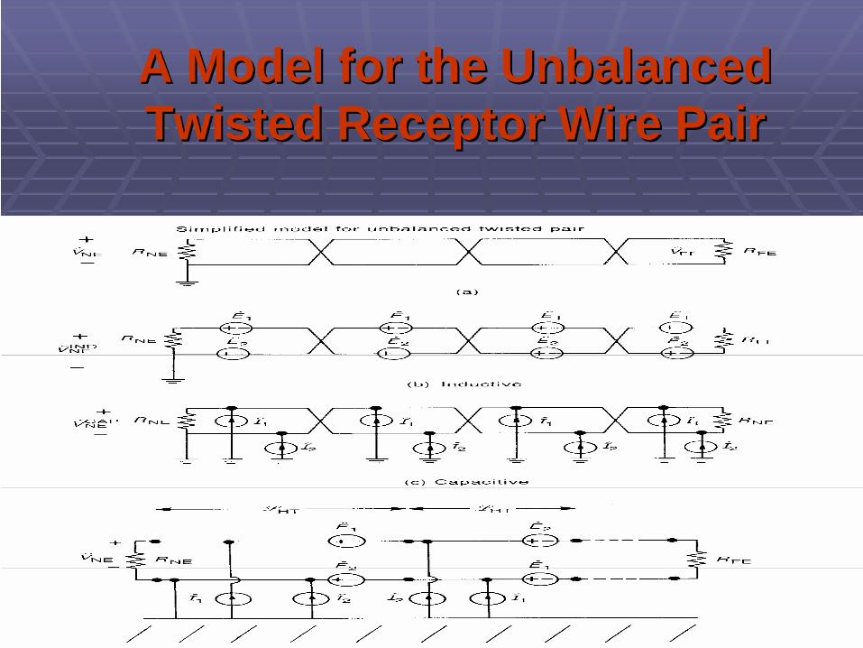
A Model for the Unbalanced A Model for the Unbalanced Twisted Receptor Wire PairTwisted Receptor Wire Pair

Explanation of the EffectExplanation of the Effectof an Unbalanced Twisted Pairof an Unbalanced Twisted Pair

The Three Levels of The Three Levels of Reducing Inductive CrosstalkReducing Inductive Crosstalk
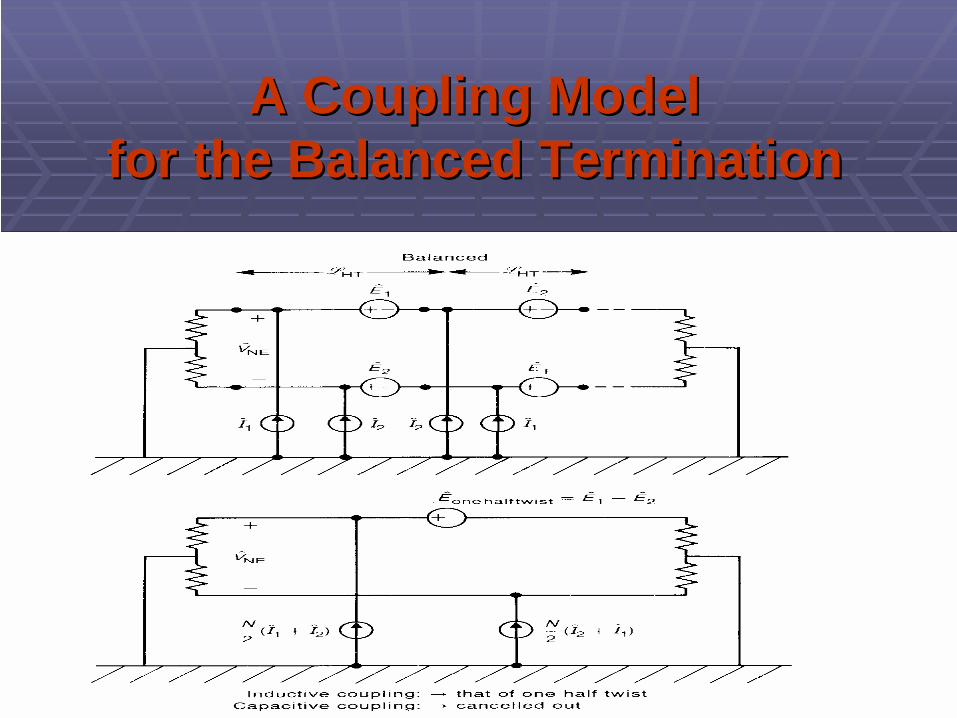
A Coupling ModelA Coupling Modelfor the Balanced Terminationfor the Balanced Termination
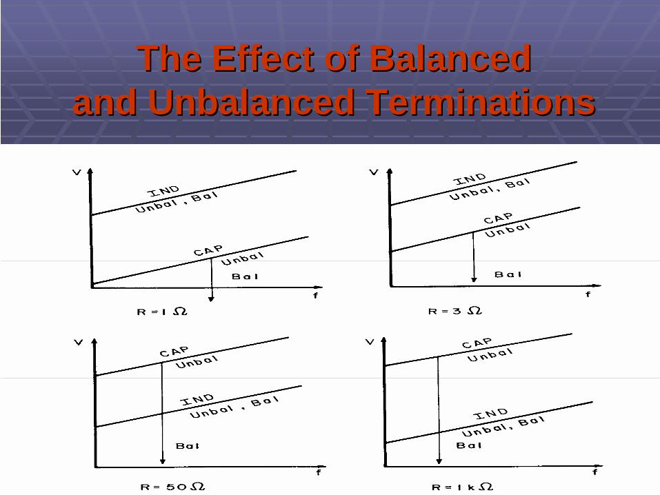
The Effect of BalancedThe Effect of Balancedand Unbalanced Terminationsand Unbalanced Terminations

Purposes of a ShieldPurposes of a Shield
To prevent the emissions of the electronicsof the product from radiating outside the boundaries of the productTo prevent radiated emissions external to the product from coupling to the product’s electronics

Degradation of Shielding Degradation of Shielding EffectivenessEffectiveness
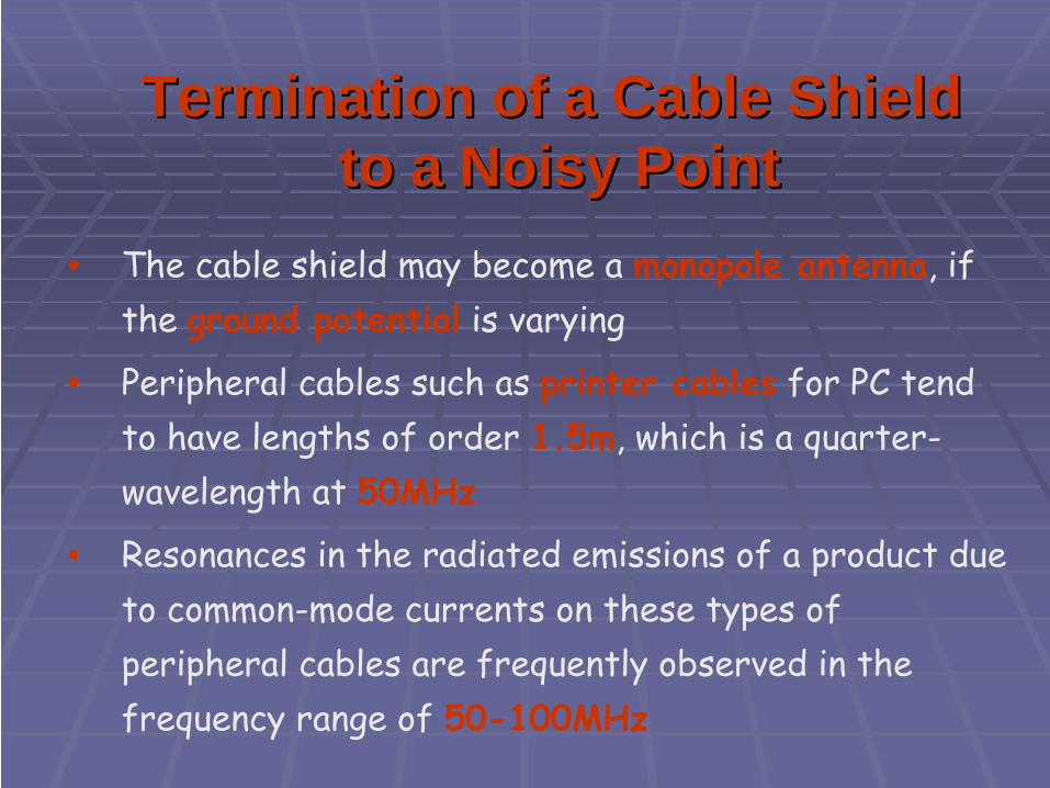
The cable shield may become a monopole antenna, if the ground potential is varying
Peripheral cables such as printer cables for PC tend to have lengths of order 1.5m, which is a quarter-wavelength at 50MHz
Resonances in the radiated emissions of a product due to common-mode currents on these types of peripheral cables are frequently observed in the frequency range of 50-100MHz
Termination of a Cable ShieldTermination of a Cable Shieldto a Noisy Pointto a Noisy Point
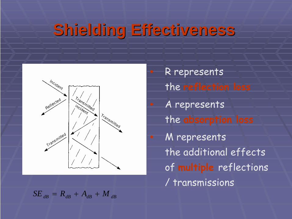
Shielding EffectivenessShielding Effectiveness
dBdBdBdB MARSE ++=
R represents the reflection loss
A represents the absorption loss
M represents the additional effects of multiple reflections / transmissions
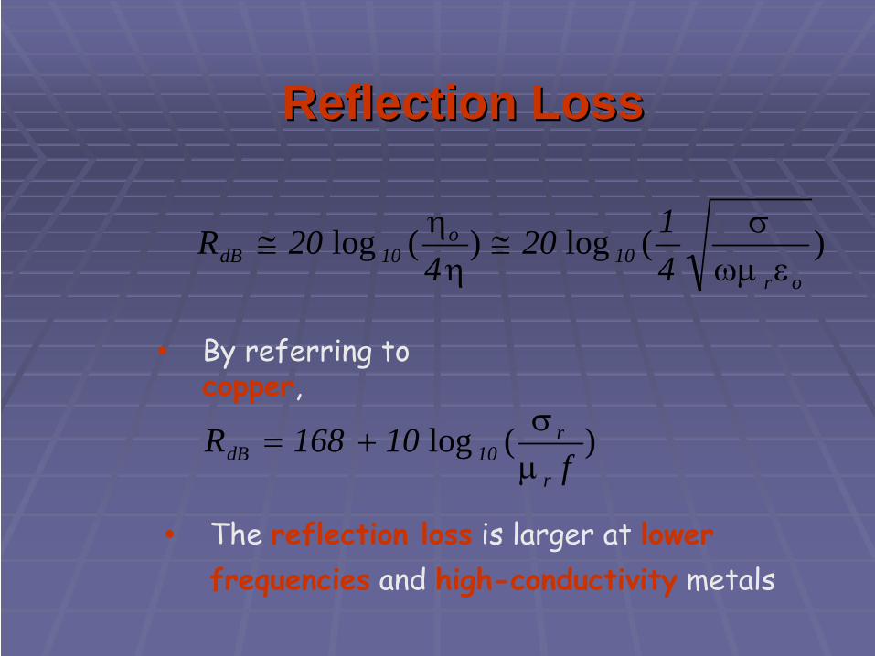
Reflection Loss Reflection Loss
)(log)(logor
10o
10dB 4120
420R
εωμσ
≅ηη
≅
By referring to copper,
)(logf
10168Rr
r10dB μ
σ+=
The reflection loss is larger at lower frequencies and high-conductivity metals
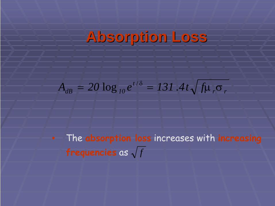
Absorption Loss Absorption Loss
rrt
10dB ft4131e20A σμ== δ .log /
The absorption loss increases with increasing frequencies as f
Shielding EffectivenessShielding Effectiveness

Shielding EffectivenessShielding Effectiveness
Reflection loss is the primary contributor to
the shielding effectiveness at low frequencies
At the higher frequencies, ferrous materials
increase the absorption loss and the total
shielding effectiveness

Shielding Effectiveness of MetalsShielding Effectiveness of Metals
The Methods of Shielding against The Methods of Shielding against LowLow--Frequency Magnetic FieldsFrequency Magnetic Fields
The permeability of ferromagnetic materials decreases with increasing frequencyThe permeability of ferromagnetic materials decrease with increasing magnetic field strength
The Frequency DependenceThe Frequency Dependenceof Various Ferromagnetic Materialsof Various Ferromagnetic Materials
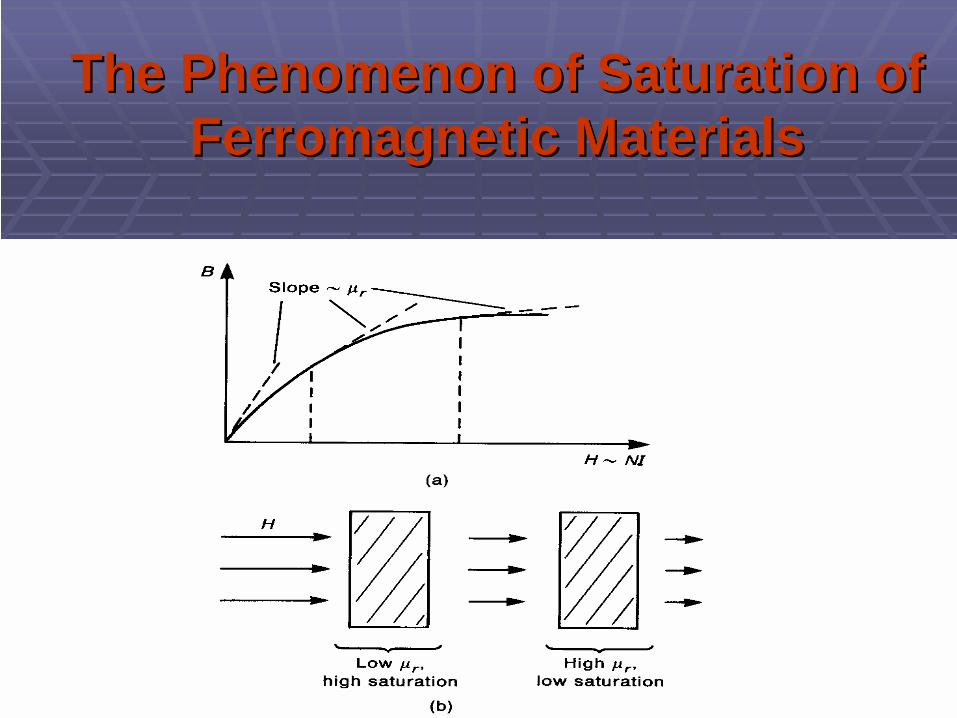
The Phenomenon of Saturation of The Phenomenon of Saturation of Ferromagnetic MaterialsFerromagnetic Materials
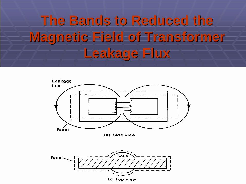
The Bands to Reduced the The Bands to Reduced the Magnetic Field of Transformer Magnetic Field of Transformer
Leakage FluxLeakage Flux
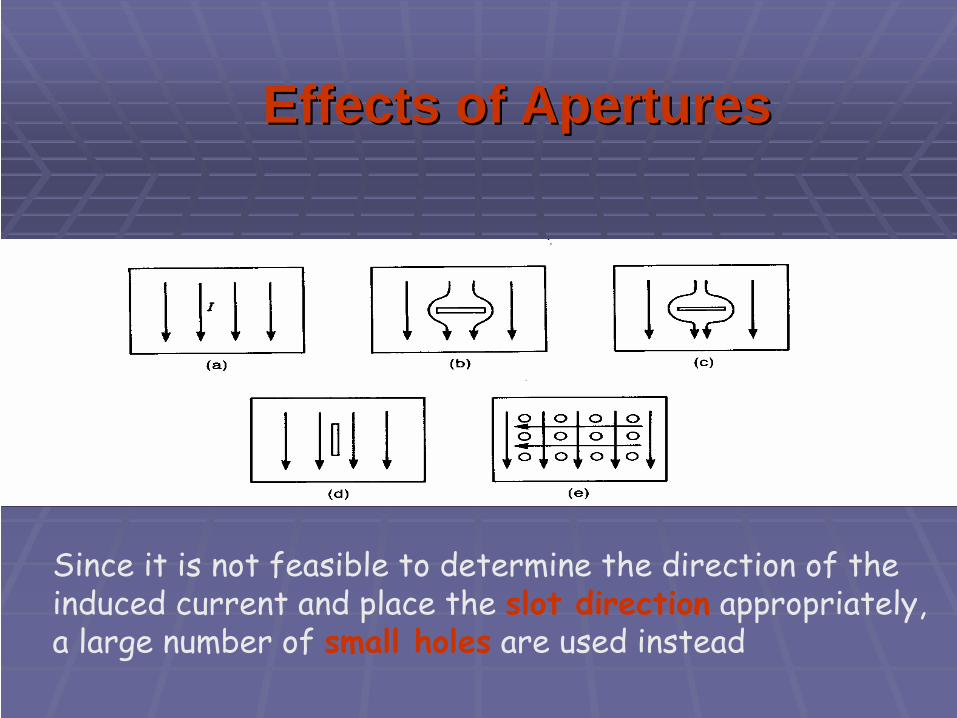
Effects of AperturesEffects of Apertures
Since it is not feasible to determine the direction of the induced current and place the slot direction
appropriately,
a large number of small holes
are used instead
ESD EventsESD Events
Typical rise times are of order 200ps-70ns, with a total duration of around 100ns-2μs
The peak levels may approach tens of amps for a voltage difference of 10kV
The spectral content of the arc may have large amplitudes, and can extend well into the GHz frequency range
Effects of the ESD EventsEffects of the ESD Events
The intense electrostatic field created by the charge separation prior to the ESD arc
The intense arc discharge current
Three Techniques for Preventing Three Techniques for Preventing Problems Caused by an ESD EventProblems Caused by an ESD Event
Prevent occurrence of the ESD event
Prevent or reduce the coupling (conduction or radiation) to the electronic circuitry of the product (hardware immunity)
Create an inherent immunity to the ESD event in the electronic circuitry through software (software immunity)
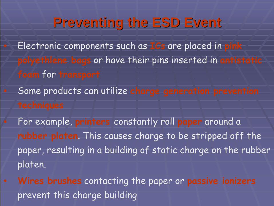
Preventing the ESD EventPreventing the ESD EventElectronic components such as ICs are placed in pink polyethlene bags or have their pins inserted in antistatic foam for transport
Some products can utilize charge generation prevention techniques
For example, printers constantly roll paper around a rubber platen. This causes charge to be stripped off the paper, resulting in a building of static charge on the rubber platen.
Wires brushes contacting the paper or passive ionizersprevent this charge building

Hardware ImmunityHardware Immunity
Secondary arc discharges
Direct conduction
Electric field (Capacitive) coupling
Magnetic field (Inductive) coupling
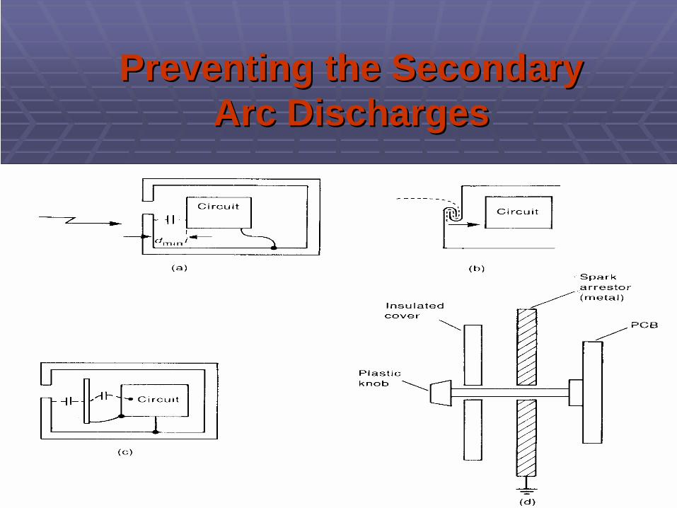
Preventing the SecondaryPreventing the SecondaryArc DischargesArc Discharges
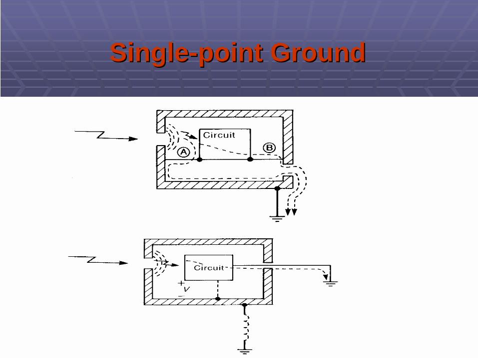
SingleSingle--point Groundpoint Ground

Use of Shielded Cables to Use of Shielded Cables to Exclude ESD CouplingExclude ESD Coupling

The Methods of PreventingThe Methods of PreventingESDESD--induced Currentsinduced Currents

Reduction of Loop Area inReduction of Loop Area inPower Distribution Circuits Power Distribution Circuits
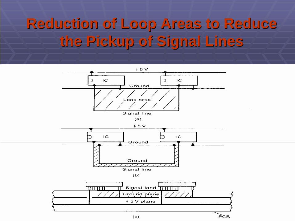
Reduction of Loop Areas to Reduce Reduction of Loop Areas to Reduce the Pickup of Signal Linesthe Pickup of Signal Lines
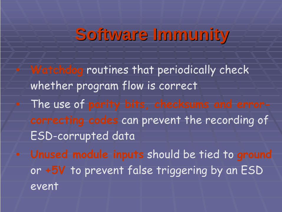
Software ImmunitySoftware Immunity
Watchdog routines that periodically check whether program flow is correctThe use of parity bits, checksums and error-correcting codes can prevent the recording of ESD-corrupted dataUnused module inputs should be tied to groundor +5V to prevent false triggering by an ESD event

Packaging Consideration Packaging Consideration
A critical aspect of incorporating good EMC design is an awareness of these nonideal effects throughout the functional design processAnother critical aspect in successful EMC design of a system is to not place reliance on “brute force fixes”such as “shielding” and “grounding”
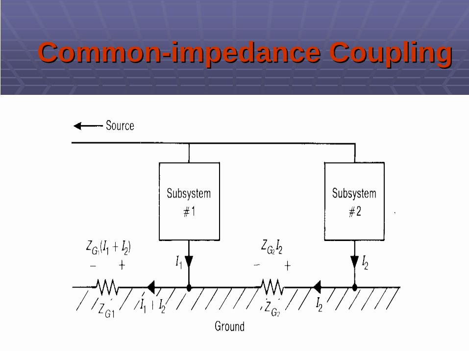
CommonCommon--impedance Couplingimpedance Coupling
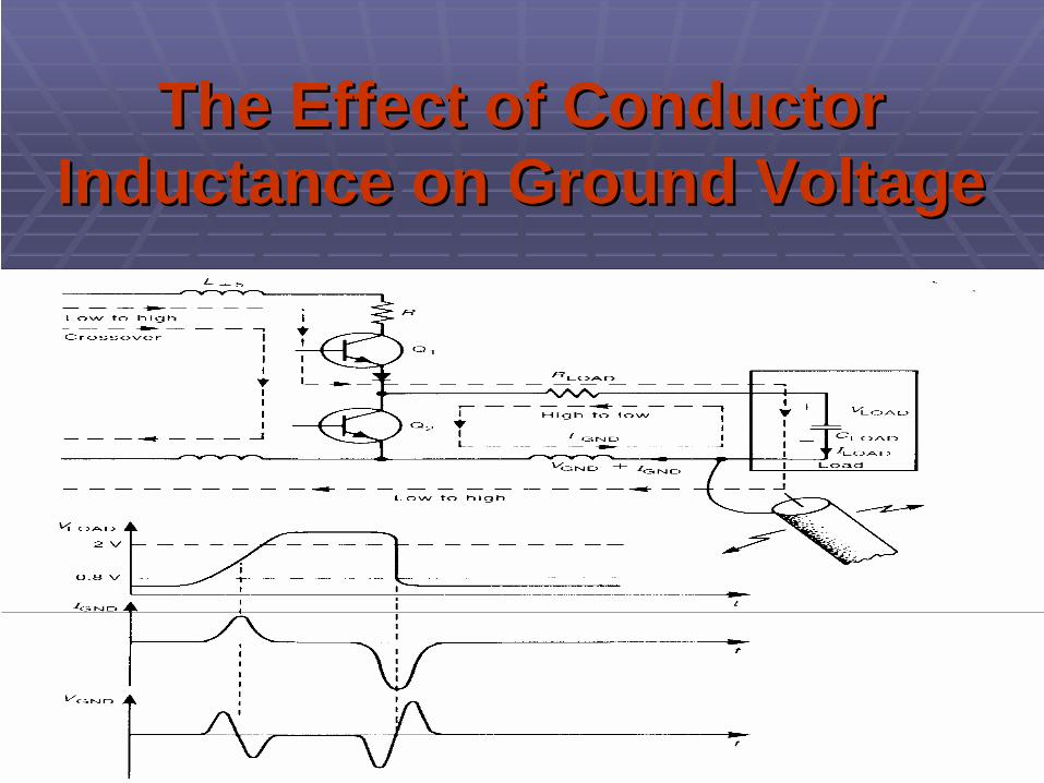
The Effect of Conductor The Effect of Conductor Inductance on Ground VoltageInductance on Ground Voltage
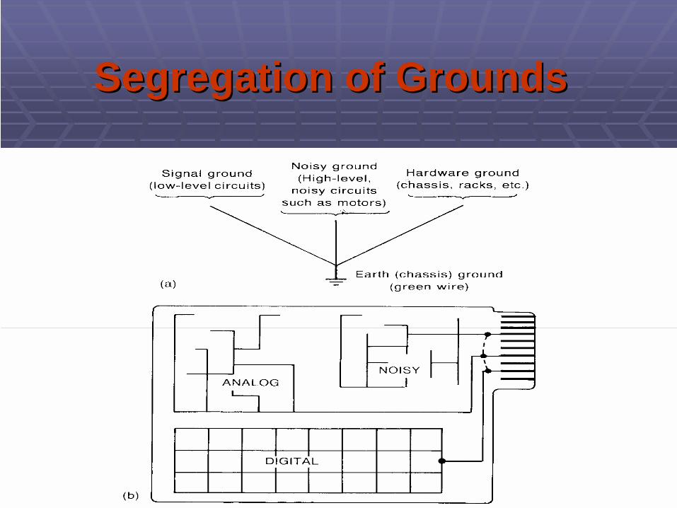
Segregation of GroundsSegregation of Grounds
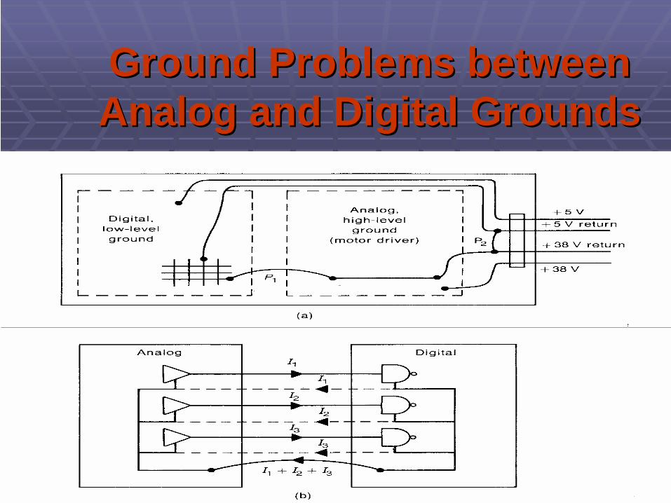
Ground Problems between Ground Problems between Analog and Digital GroundsAnalog and Digital Grounds
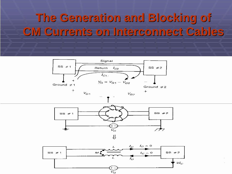
The Generation and Blocking ofThe Generation and Blocking ofCM Currents on Interconnect CablesCM Currents on Interconnect Cables
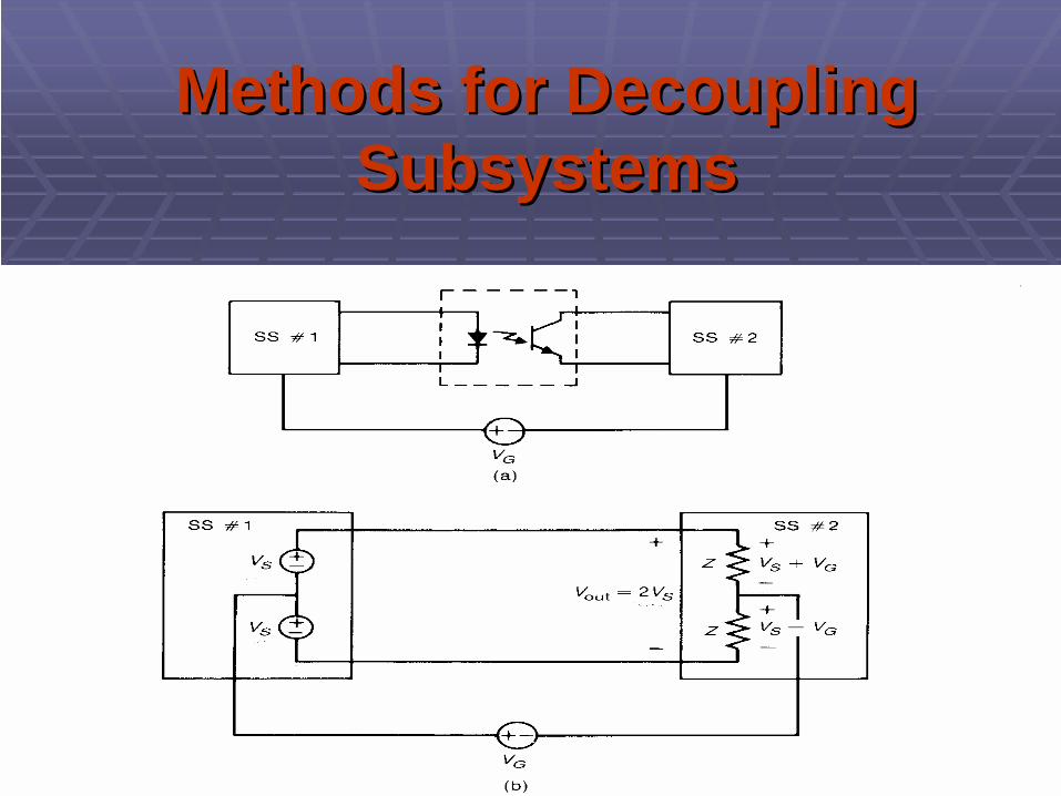
Methods for Decoupling Methods for Decoupling SubsystemsSubsystems

Interconnection and Interconnection and Number of PCBsNumber of PCBs
It is preferable to have only one system PCB rather than several smaller PCBs interconnected by cablesThe PCBs can be interconnected by plugging their edge connectors into the motherboard

Use of Interspersed Grounds Use of Interspersed Grounds to Reduce Loop Areasto Reduce Loop Areas
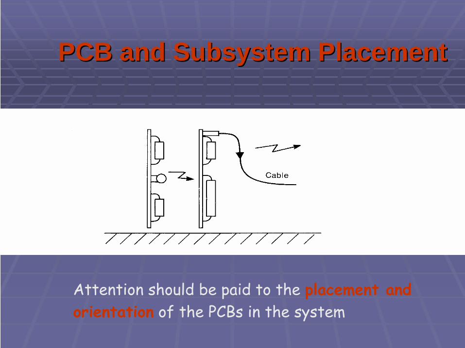
PCB and Subsystem PlacementPCB and Subsystem Placement
Attention should be paid to the placement and orientation
of the PCBs in the system
Decoupling SubsystemsDecoupling Subsystems
Common-mode currents flowing between subsystems can be effectively blocked with ferrite, common-mode chokes
Another method of decoupling subsystems is insert a filter in the connection wires or lands between the subsystems. This filter can be in the form of R-C packs, ferrite beads, or a combination
High-frequency signals on the power distribution systembetween subsystems can be reduced by the use of decoupling capacitors

Splitting Crystal/ Oscillator FrequenciesSplitting Crystal/ Oscillator Frequencies
The 16th harmonics (32MHz and 31.696MHz) are separated by 304kHz, so that they will not add in the bandwidth of the receiverThe 100th harmonic of the 2MHz signal (200MHz) and the 101st
harmonic of the 1.981MHz signal (200.081MHz) will be within81kHz of each other and will add in the bandwidth of the receiver

Component PlacementComponent Placement
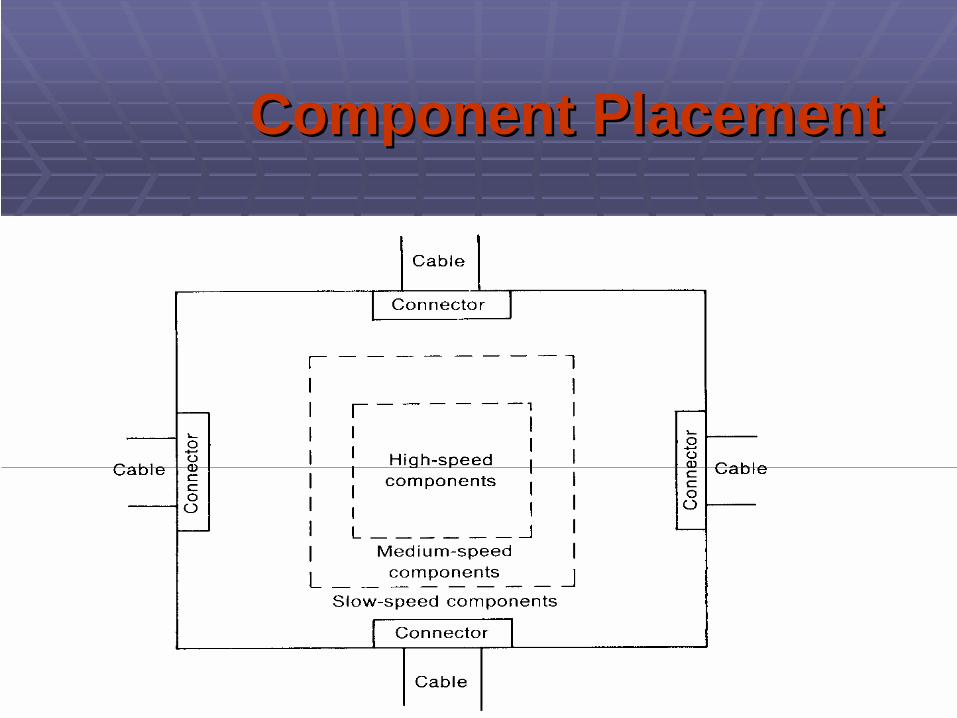
Component PlacementComponent Placement

A Good Layout for a A Good Layout for a Typical Digital SystemTypical Digital System
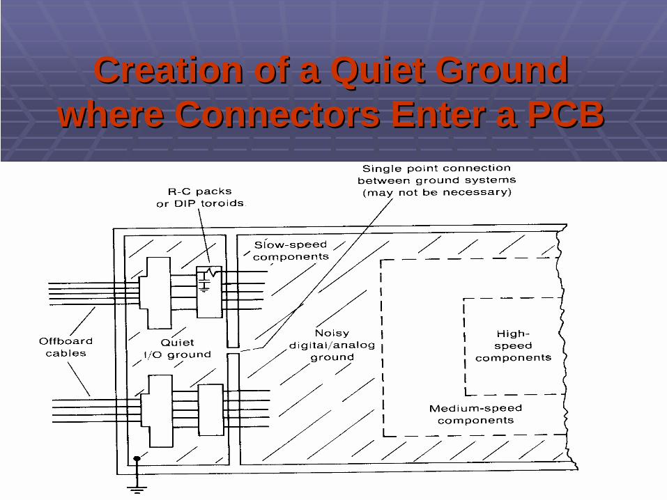
Creation of a Quiet Ground Creation of a Quiet Ground where Connectors Enter a PCBwhere Connectors Enter a PCB
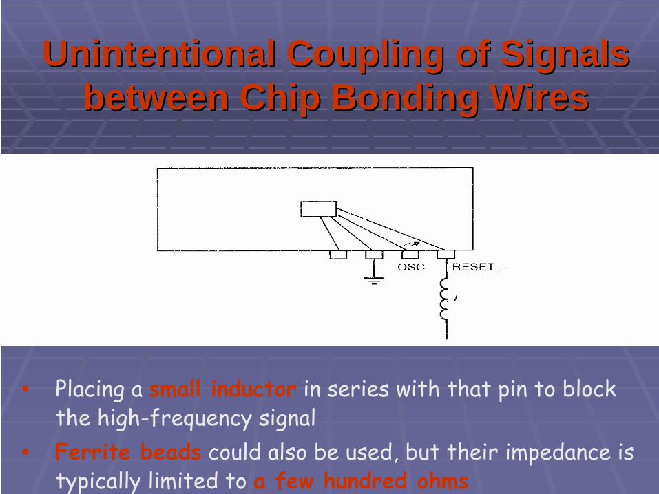
Unintentional Coupling of Signals Unintentional Coupling of Signals between Chip Bonding Wiresbetween Chip Bonding Wires
Placing a small inductor in series with that pin to block the high-frequency signalFerrite beads could also be used, but their impedance is typically limited to a few hundred ohms

Use of Decoupling CapacitorsUse of Decoupling Capacitors

Decoupling Capacitor PlacementDecoupling Capacitor Placement
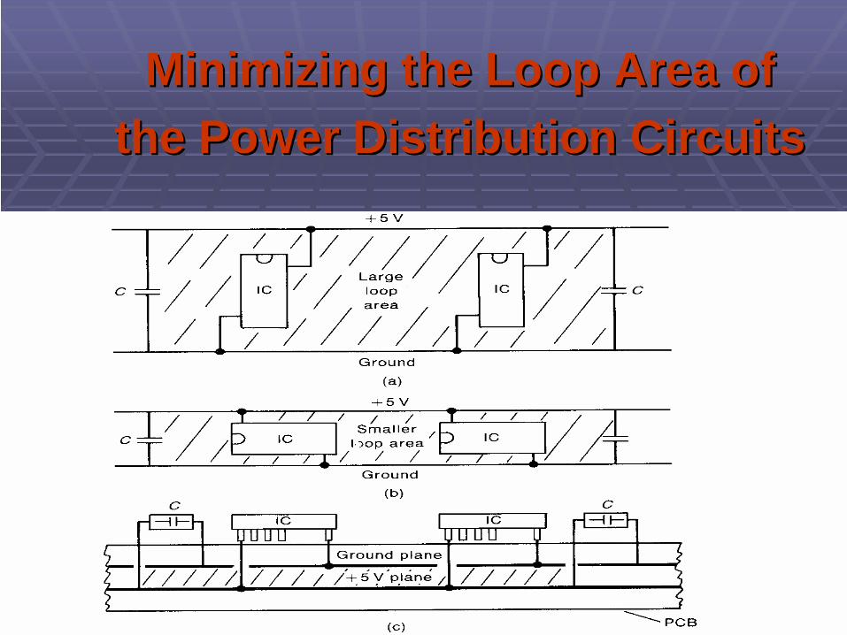
Minimizing the Loop Area ofMinimizing the Loop Area ofthe Power Distribution Circuitsthe Power Distribution Circuits

![diagramas.diagramasde.comdiagramas.diagramasde.com/otros/sistema_elect_audio[1].pdf · modelo DC 522 INDICE MODE-LO DC 522 1. SEGURIDALD Esta unidad posee las stguientes caracte-](https://img.pdfslide.tips/doc/110x75/5f6dfa54e2931769252d0297/1pdf-modelo-dc-522-indice-mode-lo-dc-522-1-seguridald-esta-unidad-posee-las.jpg)


![Internet Radio Internetradio · 1 Controls and Displays A: Front 1 Display 2 [ ] On/off switch 3 [INFO] Display additional information 4 [MODE] Changing operating mode (Internet radio,](https://img.pdfslide.tips/doc/110x75/5fb06ac9d6b62416926432c9/internet-radio-internetradio-1-controls-and-displays-a-front-1-display-2-onoff.jpg)