Embed Size (px)
Citation preview
Eu
Wa
b
c
a
ARRAA
KPSIE(EA
1
tttnofACanbifiug
tT
0h
Progress in Organic Coatings 77 (2014) 537– 547
Contents lists available at ScienceDirect
Progress in Organic Coatings
jou rn al hom ep age: www.elsev ier .com/ locate /porgcoat
valuation of sub-micrometer parylene C films as an insulation layersing electrochemical impedance spectroscopy
onju Chuna, Namsun Choub, Sungbo Choc, Sung Yanga,b, Sohee Kima,b,∗
Dept. of Medical System Engineering, Gwangju Institute of Science and Technology, Gwangju, Republic of KoreaSchool of Mechatronics, Gwangju Institute of Science and Technology, Gwangju, Republic of KoreaDept. of Biomedical Engineering, Gachon University, Incheon, Republic of Korea
r t i c l e i n f o
rticle history:eceived 1 February 2013eceived in revised form 23 October 2013ccepted 19 November 2013vailable online 9 December 2013
eywords:arylene C
a b s t r a c t
We investigated the insulation performance of sub-micrometer parylene C films over time usingelectrochemical impedance spectroscopy (EIS). For this, interdigitated electrodes were fabricated andcompletely encapsulated with parylene C in thicknesses of 50, 100, 200, and 500 nm. The EIS was mea-sured in phosphate buffered saline (PBS) solution under an accelerated aging condition at 90 ◦C over45 days. To analyze the EIS data, the equivalent circuit models of coating at different stages of coatingdegradation were used and the lumped circuit parameters of the best fitted equivalent circuit modelwere extracted by curve fitting. The analysis of impedance using the equivalent circuit model and the
ub-micrometernsulationlectrochemical impedance spectroscopyEIS)quivalent circuit modelccelerated soak test
FTIR measurements suggest that sub-micrometer parylene C coatings exhibited delamination result-ing from water diffusion from the top surface as soon as being immersed in PBS solution, although thedegree of delamination varied depending on the film thickness. The penetration of water through sub-micrometers thick parylene C films can occur as quickly as the film is in contact with solution, unlike forthicker coatings in several micrometers where water diffusion would be saturated before water reachesthe bottom surface of the coating.
© 2013 Elsevier B.V. All rights reserved.
. Introduction
Recently, there has been a growing interest in the encapsula-ion of implantable devices or the insulation of bioelectric sensorso shield them from harsh, corrosive biofluidic environments ando protect the living tissue against the corrosion products andon-biocompatible materials. It is required that the encapsulationr insulation be hermetic, biocompatible, weightless and flexibleor the micrometer-sized implantable devices and sensors [1,2].mong packaging materials, parylene (poly-para-xylylene (PPX))
has been frequently used in coating cardiac pacemakers [3,4]nd in neuro-technology such as microwires to record neural sig-als [5–7] and micromachined neural electrode arrays [8–11]. It isecause of its desirable characteristics such that it is chemically
nert, non-toxic, non-biodegradable, biocompatible to be classi-
ed as USP (U.S. Pharmacopeia) class VI plastics, with which thesage in implantable devices is certified. It shows low water andas permeability, low dielectric constant and high resistivity. It can∗ Corresponding author at: Dept. of Medical System Engineering, School of Mecha-ronics, Gwangju Institute of Science and Technology, Gwangju, Republic of Korea.el.: +82 62 715 3224.
E-mail address: [email protected] (S. Kim).
300-9440/$ – see front matter © 2013 Elsevier B.V. All rights reserved.ttp://dx.doi.org/10.1016/j.porgcoat.2013.11.020
be conformally coated on surfaces by a pinhole-free, solventlesschemical vapor deposition (CVD) polymerization process [12].
As the thickness of coating increases, the durability of insula-tion or encapsulation is correspondingly increased whereas issuesrelated with the volume and flexibility of the implanted devices orthe sensitivity of the electrode-based sensors should be taken intoaccount. When the electrodes recessed by the insulating materialsis positioned in the body region of interest, the separated distancebetween the electrode surface and the tissue to be measured orstimulated may be increased with the increasing thickness of theinsulation layer, which results in the signal distortion or attenua-tion. In case of the capacitive sensors that measure the capacitiveproperty of the probe layer on the insulation layer coating the elec-trodes, the measurement sensitivity on the probe layer is decreasedas the thickness of the insulation layer increases [13,14]. While theaforementioned issues can be improved by decreasing the thick-ness of the insulation layer, it is required to periodically checkthe insulation properties of thin coating materials to guaranteethe function of the sensors or implanted devices especially whenthey are intended for long-term use. More recently, thin parylene
films have been used in encapsulation of organic light-emitting-diode (OLED) devices [15–17] and organic thin film transistors[18], where it should act as a superior barrier against chemi-cals and moisture, and guarantee optical transparency. Besides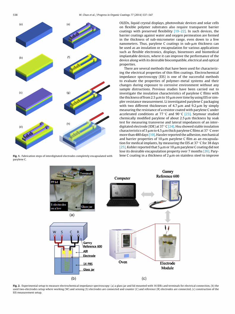
538 W. Chun et al. / Progress in Organic
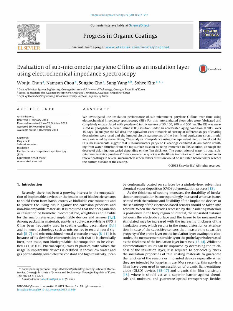
Fig. 1. Fabrication steps of interdigitated electrodes completely encapsulated withparylene C.
Fig. 2. Experimental setup to measure electrochemical impedance spectroscopy: (a) a glaused two-electrodes setup where working (W) and sensing (S) electrodes are connected
EIS measurement setup.
Coatings 77 (2014) 537– 547
OLEDs, liquid crystal displays, photovoltaic devices and solar cellson flexible polymer substrates also require transparent barriercoatings with preserved flexibility [19–22]. In such devices, thebarrier coatings against water and oxygen permeation are formedin the thickness of sub-micrometer range, even down to a fewnanometers. Thus, parylene C coatings in sub-�m thickness canbe used as an insulation or encapsulation for various applicationssuch as flexible electronics, displays, biosensors and biomedicalimplantable devices, where it can improve the performance of thedevice along with its desirable biocompatible, electrical and opticalproperties.
There are several methods that have been used for characteriz-ing the electrical properties of thin film coatings. Electrochemicalimpedance spectroscopy (EIS) is one of the successful methodsto evaluate the properties of polymer–metal systems and theirchanges during exposure to corrosive environment without anysample distructions. Previous studies have been carried out toinvestigate the insulation characteristics of parylene C films withthe thickness of from 2.5 �m to 10 �m over time by using EIS or sim-pler resistance measurement. Li investigated parylene C packagingwith two different thicknesses of 4.7 �m and 9.2 �m by simplymeasuring the resistance of a resistor coated with parylene C underaccelerated conditions at 77 ◦C and 90 ◦C [23]. Seymour studiedchemically modified parylene of about 2.5 �m thickness by soaktest for measuring transverse and lateral impedances of an inter-digitated electrode (IDE) at 37 ◦C [24]. Hsu showed stable insulationcharacteristics of 3 �m to 4.5 �m thick parylene C films at 37 ◦C overmore than 480 days [10]. Hassler reported the adhesion, mechanicaland barrier properties of 10 �m parylene C film as an encapsula-tion for medical implants, by measuring the EIS at 37 ◦C for 38 days
[25]. Kohler reported that 5 �m or 10 �m parylene C coating did notlose its desirable encapsulation property over 7 months [26]. Pary-lene C coating in a thickness of 2 �m on stainless steel to improvess jar and lid mounted with 16 IDEs and terminals for electrical connection, (b) theand counter (C) and reference (R) electrodes are connected, (c) construction of the
W. Chun et al. / Progress in Organic Coatings 77 (2014) 537– 547 539
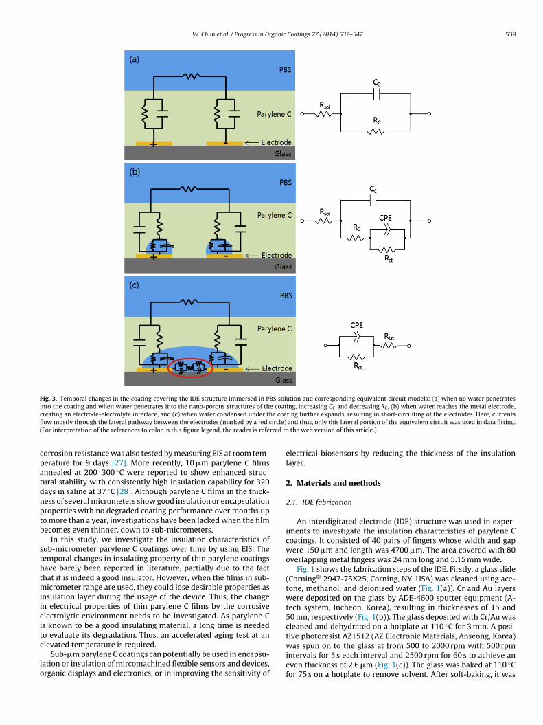
Fig. 3. Temporal changes in the coating covering the IDE structure immersed in PBS solution and corresponding equivalent circuit models: (a) when no water penetratesinto the coating and when water penetrates into the nano-porous structures of the coating, increasing CC and decreasing RC, (b) when water reaches the metal electrode,c e coafl ircle)( rred to
cpatdnptb
sthtmiieite
lo
reating an electrode-electrolyte interface, and (c) when water condensed under thow mostly through the lateral pathway between the electrodes (marked by a red cFor interpretation of the references to color in this figure legend, the reader is refe
orrosion resistance was also tested by measuring EIS at room tem-erature for 9 days [27]. More recently, 10 �m parylene C filmsnnealed at 200–300 ◦C were reported to show enhanced struc-ural stability with consistently high insulation capability for 320ays in saline at 37 ◦C [28]. Although parylene C films in the thick-ess of several micrometers show good insulation or encapsulationroperties with no degraded coating performance over months upo more than a year, investigations have been lacked when the filmecomes even thinner, down to sub-micrometers.
In this study, we investigate the insulation characteristics ofub-micrometer parylene C coatings over time by using EIS. Theemporal changes in insulating property of thin parylene coatingsave barely been reported in literature, partially due to the facthat it is indeed a good insulator. However, when the films in sub-
icrometer range are used, they could lose desirable properties asnsulation layer during the usage of the device. Thus, the changen electrical properties of thin parylene C films by the corrosivelectrolytic environment needs to be investigated. As parylene Cs known to be a good insulating material, a long time is neededo evaluate its degradation. Thus, an accelerated aging test at an
levated temperature is required.Sub-�m parylene C coatings can potentially be used in encapsu-ation or insulation of mircomachined flexible sensors and devices,rganic displays and electronics, or in improving the sensitivity of
ting further expands, resulting in short-circuiting of the electrodes. Here, currents and thus, only this lateral portion of the equivalent circuit was used in data fitting.
the web version of this article.)
electrical biosensors by reducing the thickness of the insulationlayer.
2. Materials and methods
2.1. IDE fabrication
An interdigitated electrode (IDE) structure was used in exper-iments to investigate the insulation characteristics of parylene Ccoatings. It consisted of 40 pairs of fingers whose width and gapwere 150 �m and length was 4700 �m. The area covered with 80overlapping metal fingers was 24 mm long and 5.15 mm wide.
Fig. 1 shows the fabrication steps of the IDE. Firstly, a glass slide(Corning® 2947-75X25, Corning, NY, USA) was cleaned using ace-tone, methanol, and deionized water (Fig. 1(a)). Cr and Au layerswere deposited on the glass by ADE-4600 sputter equipment (A-tech system, Incheon, Korea), resulting in thicknesses of 15 and50 nm, respectively (Fig. 1(b)). The glass deposited with Cr/Au wascleaned and dehydrated on a hotplate at 110 ◦C for 3 min. A posi-tive photoresist AZ1512 (AZ Electronic Materials, Anseong, Korea)
was spun on to the glass at from 500 to 2000 rpm with 500 rpmintervals for 5 s each interval and 2500 rpm for 60 s to achieve aneven thickness of 2.6 �m (Fig. 1(c)). The glass was baked at 110 ◦Cfor 75 s on a hotplate to remove solvent. After soft-baking, it was
540 W. Chun et al. / Progress in Organic Coatings 77 (2014) 537– 547
hs of a fabricated IDE.
e4MteatmNwawpta(ndrtIrfdbs
cntdetIiwst
2
lCfiobiimMt
Fig. 4. Photograp
xposed to UV light (15 mJ/cm2 s) for 7 s by a mask aligner MDA-00M (MIDAS System Ltd., Daejeon, Korea). It was developed inIF 300 developer for 75 s with high agitation (Fig. 1(d)). The elec-
rode pattern was obtained by wet etching of Cr and Au usingtchant (Fig. 1(e)). Residual photoresist was removed by acetonend the electrode was cleaned (Fig. 1(f)). Wires were attached onhe contact pads to connect the electrodes to measurement equip-
ent using a conductive epoxy (DURALCOTM 125, Cotronics Corp.,Y, USA). An epoxy adhesive (5 Minute® Epoxy, Devcon, MA, USA)as applied to contact pads and wires in order to prevent water
nd vapor attack during soak test (Fig. 1(g)). Finally, parylene Cas uniformly deposited on the IDE and the glass slide by a CVDolymerization process using PDS 2010 chemical deposition sys-em (Specialty Coating System Inc., Indianapolis, IN, USA) after thepplication of adhesion promoter A-174 silane to improve adhesionFig. 1(h)). Parylene C coating was formed in four target thick-esses of 50, 100, 200, and 500 nm by controlling the amount ofimer. The used amounts of dimer were 0.06, 0.12, 0.24, and 0.58 g,espectively. The resulted film thicknesses were measured on par-ially marked dummy samples using a surface profiler Alpha-StepQ (KLA-Tencor Corp., Milpitas, CA, USA). The deviations in theesulted coating thickness were measured to be less than ±15 nmor all thicknesses except for 50 nm coating that showed a largereviation. The pressure in the deposition chamber was maintainedetween 6 and 10 mTorr throughout the overall process. The depo-ition rate was about 14 nm/min.
We used a glass substrate to fabricate the IDE for easier opti-al detection and simplified fabrication procedure by removing theeed for an electrical insulation layer between the electrodes andhe substrate, which is generally required when using a semicon-uctor substrate. Also, the fabrication process was simplified byliminating the step of reactive ion etching (RIE) to open the con-act pads since parylene C was deposited after wiring contact pads.t resulted in a completely encapsulated IDE structure without leav-ng any surfaces or interfaces exposed to the environment. It is
orth mentioning that this structure prevents direct water diffu-ion into the metal–parylene interface, which has been identifiedo be the likely cause of coating failure [19,24,28].
.2. Experimental setup for EIS
The soak test setup consisted of a glass jar, a polypropylene (PP)id, electrical terminals, and four sets of IDEs coated with parylene
in four different thicknesses. For each thickness of parylene Clm, four IDEs were stacked up on a handmade fixture at intervalsf 6.5 mm (Fig. 2(a)). The glass jar was filled with 1× phosphateuffered saline (PBS) solution and 16 IDEs in total were immersed
n it. The IDEs were wired to electrical terminals through the open-
ngs created by drilling the lid, where the electrical terminals wereounted and the openings were afterwards sealed with an epoxy (5inute® Epoxy, Devcon, MA, USA). PBS solution was replaced twice
hroughout the experiment, at 7th and 28th day, to minimize theFig. 5. SEM images of the surface of parylene C films in thicknesses of (a) 100 nm,(b) 500 nm and (c) 6 �m.
W. Chun et al. / Progress in Organic Coatings 77 (2014) 537– 547 541
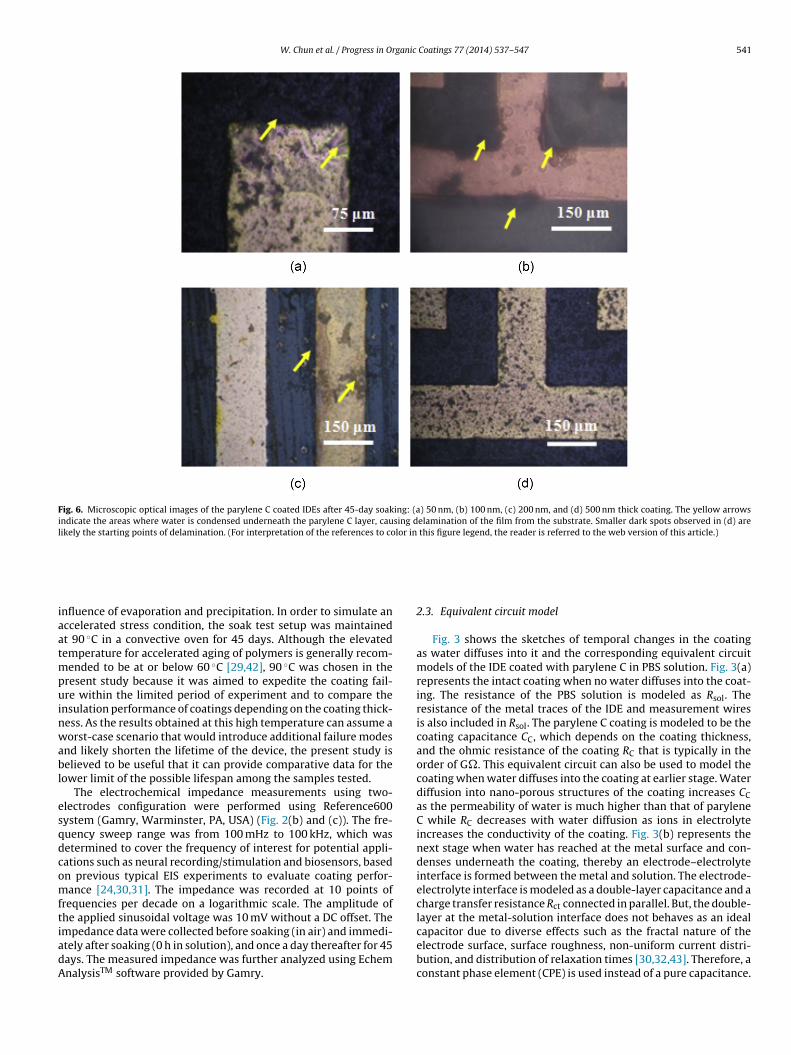
Fig. 6. Microscopic optical images of the parylene C coated IDEs after 45-day soaking: (a) 50 nm, (b) 100 nm, (c) 200 nm, and (d) 500 nm thick coating. The yellow arrowsindicate the areas where water is condensed underneath the parylene C layer, causing delamination of the film from the substrate. Smaller dark spots observed in (d) arelikely the starting points of delamination. (For interpretation of the references to color in this figure legend, the reader is referred to the web version of this article.)
iaatmpuinwabl
esqdcomftiadA
nfluence of evaporation and precipitation. In order to simulate anccelerated stress condition, the soak test setup was maintainedt 90 ◦C in a convective oven for 45 days. Although the elevatedemperature for accelerated aging of polymers is generally recom-
ended to be at or below 60 ◦C [29,42], 90 ◦C was chosen in theresent study because it was aimed to expedite the coating fail-re within the limited period of experiment and to compare the
nsulation performance of coatings depending on the coating thick-ess. As the results obtained at this high temperature can assume aorst-case scenario that would introduce additional failure modes
nd likely shorten the lifetime of the device, the present study iselieved to be useful that it can provide comparative data for the
ower limit of the possible lifespan among the samples tested.The electrochemical impedance measurements using two-
lectrodes configuration were performed using Reference600ystem (Gamry, Warminster, PA, USA) (Fig. 2(b) and (c)). The fre-uency sweep range was from 100 mHz to 100 kHz, which wasetermined to cover the frequency of interest for potential appli-ations such as neural recording/stimulation and biosensors, basedn previous typical EIS experiments to evaluate coating perfor-ance [24,30,31]. The impedance was recorded at 10 points of
requencies per decade on a logarithmic scale. The amplitude ofhe applied sinusoidal voltage was 10 mV without a DC offset. The
mpedance data were collected before soaking (in air) and immedi-tely after soaking (0 h in solution), and once a day thereafter for 45ays. The measured impedance was further analyzed using EchemnalysisTM software provided by Gamry.2.3. Equivalent circuit model
Fig. 3 shows the sketches of temporal changes in the coatingas water diffuses into it and the corresponding equivalent circuitmodels of the IDE coated with parylene C in PBS solution. Fig. 3(a)represents the intact coating when no water diffuses into the coat-ing. The resistance of the PBS solution is modeled as Rsol. Theresistance of the metal traces of the IDE and measurement wiresis also included in Rsol. The parylene C coating is modeled to be thecoating capacitance CC, which depends on the coating thickness,and the ohmic resistance of the coating RC that is typically in theorder of G�. This equivalent circuit can also be used to model thecoating when water diffuses into the coating at earlier stage. Waterdiffusion into nano-porous structures of the coating increases CCas the permeability of water is much higher than that of paryleneC while RC decreases with water diffusion as ions in electrolyteincreases the conductivity of the coating. Fig. 3(b) represents thenext stage when water has reached at the metal surface and con-denses underneath the coating, thereby an electrode–electrolyteinterface is formed between the metal and solution. The electrode-electrolyte interface is modeled as a double-layer capacitance and acharge transfer resistance Rct connected in parallel. But, the double-layer at the metal-solution interface does not behaves as an ideal
capacitor due to diverse effects such as the fractal nature of theelectrode surface, surface roughness, non-uniform current distri-bution, and distribution of relaxation times [30,32,43]. Therefore, aconstant phase element (CPE) is used instead of a pure capacitance.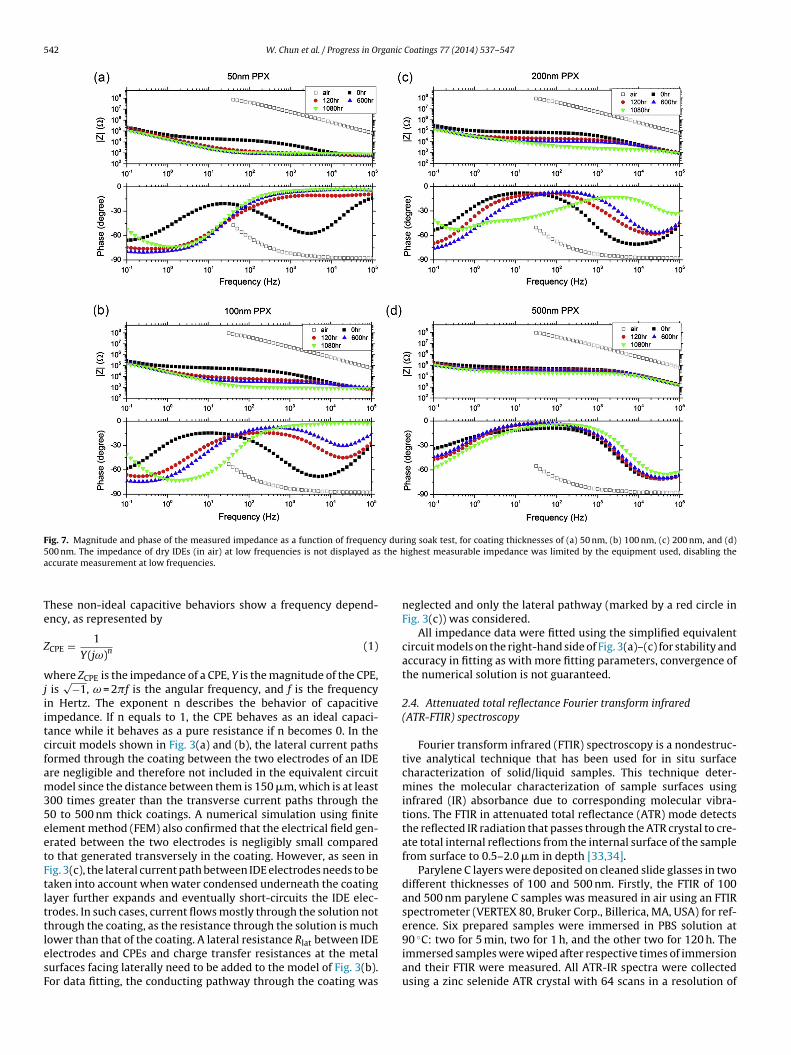
542 W. Chun et al. / Progress in Organic Coatings 77 (2014) 537– 547
Fig. 7. Magnitude and phase of the measured impedance as a function of frequency during soak test, for coating thicknesses of (a) 50 nm, (b) 100 nm, (c) 200 nm, and (d)5 the ha
Te
Z
wjiitcfam35eetFtlttlesF
00 nm. The impedance of dry IDEs (in air) at low frequencies is not displayed asccurate measurement at low frequencies.
hese non-ideal capacitive behaviors show a frequency depend-ncy, as represented by
CPE = 1Y(jω)n (1)
here ZCPE is the impedance of a CPE, Y is the magnitude of the CPE, is
√−1, ω = 2�f is the angular frequency, and f is the frequencyn Hertz. The exponent n describes the behavior of capacitivempedance. If n equals to 1, the CPE behaves as an ideal capaci-ance while it behaves as a pure resistance if n becomes 0. In theircuit models shown in Fig. 3(a) and (b), the lateral current pathsormed through the coating between the two electrodes of an IDEre negligible and therefore not included in the equivalent circuitodel since the distance between them is 150 �m, which is at least
00 times greater than the transverse current paths through the0 to 500 nm thick coatings. A numerical simulation using finitelement method (FEM) also confirmed that the electrical field gen-rated between the two electrodes is negligibly small comparedo that generated transversely in the coating. However, as seen inig. 3(c), the lateral current path between IDE electrodes needs to beaken into account when water condensed underneath the coatingayer further expands and eventually short-circuits the IDE elec-rodes. In such cases, current flows mostly through the solution nothrough the coating, as the resistance through the solution is much
ower than that of the coating. A lateral resistance Rlat between IDElectrodes and CPEs and charge transfer resistances at the metalurfaces facing laterally need to be added to the model of Fig. 3(b).or data fitting, the conducting pathway through the coating wasighest measurable impedance was limited by the equipment used, disabling the
neglected and only the lateral pathway (marked by a red circle inFig. 3(c)) was considered.
All impedance data were fitted using the simplified equivalentcircuit models on the right-hand side of Fig. 3(a)–(c) for stability andaccuracy in fitting as with more fitting parameters, convergence ofthe numerical solution is not guaranteed.
2.4. Attenuated total reflectance Fourier transform infrared(ATR-FTIR) spectroscopy
Fourier transform infrared (FTIR) spectroscopy is a nondestruc-tive analytical technique that has been used for in situ surfacecharacterization of solid/liquid samples. This technique deter-mines the molecular characterization of sample surfaces usinginfrared (IR) absorbance due to corresponding molecular vibra-tions. The FTIR in attenuated total reflectance (ATR) mode detectsthe reflected IR radiation that passes through the ATR crystal to cre-ate total internal reflections from the internal surface of the samplefrom surface to 0.5–2.0 �m in depth [33,34].
Parylene C layers were deposited on cleaned slide glasses in twodifferent thicknesses of 100 and 500 nm. Firstly, the FTIR of 100and 500 nm parylene C samples was measured in air using an FTIRspectrometer (VERTEX 80, Bruker Corp., Billerica, MA, USA) for ref-erence. Six prepared samples were immersed in PBS solution at
90 ◦C: two for 5 min, two for 1 h, and the other two for 120 h. Theimmersed samples were wiped after respective times of immersionand their FTIR were measured. All ATR-IR spectra were collectedusing a zinc selenide ATR crystal with 64 scans in a resolution of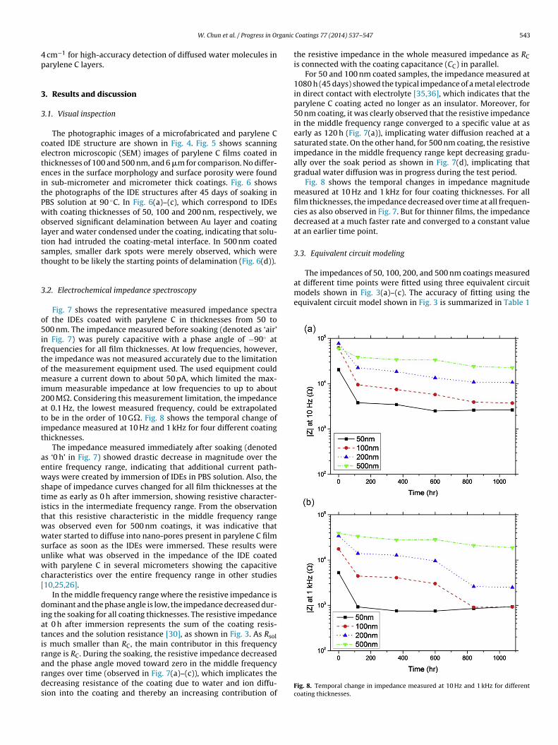
ganic
4p
3
3
ceteitPwoltst
3
o5iftomi2atit
aewstitwwsuwc[
diatirards
The impedances of 50, 100, 200, and 500 nm coatings measuredat different time points were fitted using three equivalent circuitmodels shown in Fig. 3(a)–(c). The accuracy of fitting using theequivalent circuit model shown in Fig. 3 is summarized in Table 1
W. Chun et al. / Progress in Or
cm−1 for high-accuracy detection of diffused water molecules inarylene C layers.
. Results and discussion
.1. Visual inspection
The photographic images of a microfabricated and parylene Coated IDE structure are shown in Fig. 4. Fig. 5 shows scanninglectron microscopic (SEM) images of parylene C films coated inhicknesses of 100 and 500 nm, and 6 �m for comparison. No differ-nces in the surface morphology and surface porosity were foundn sub-micrometer and micrometer thick coatings. Fig. 6 showshe photographs of the IDE structures after 45 days of soaking inBS solution at 90 ◦C. In Fig. 6(a)–(c), which correspond to IDEsith coating thicknesses of 50, 100 and 200 nm, respectively, we
bserved significant delamination between Au layer and coatingayer and water condensed under the coating, indicating that solu-ion had intruded the coating-metal interface. In 500 nm coatedamples, smaller dark spots were merely observed, which werehought to be likely the starting points of delamination (Fig. 6(d)).
.2. Electrochemical impedance spectroscopy
Fig. 7 shows the representative measured impedance spectraf the IDEs coated with parylene C in thicknesses from 50 to00 nm. The impedance measured before soaking (denoted as ‘air’
n Fig. 7) was purely capacitive with a phase angle of −90◦ atrequencies for all film thicknesses. At low frequencies, however,he impedance was not measured accurately due to the limitationf the measurement equipment used. The used equipment couldeasure a current down to about 50 pA, which limited the max-
mum measurable impedance at low frequencies to up to about00 M�. Considering this measurement limitation, the impedancet 0.1 Hz, the lowest measured frequency, could be extrapolatedo be in the order of 10 G�. Fig. 8 shows the temporal change ofmpedance measured at 10 Hz and 1 kHz for four different coatinghicknesses.
The impedance measured immediately after soaking (denoteds ‘0 h’ in Fig. 7) showed drastic decrease in magnitude over thentire frequency range, indicating that additional current path-ays were created by immersion of IDEs in PBS solution. Also, the
hape of impedance curves changed for all film thicknesses at theime as early as 0 h after immersion, showing resistive character-stics in the intermediate frequency range. From the observationhat this resistive characteristic in the middle frequency rangeas observed even for 500 nm coatings, it was indicative thatater started to diffuse into nano-pores present in parylene C film
urface as soon as the IDEs were immersed. These results werenlike what was observed in the impedance of the IDE coatedith parylene C in several micrometers showing the capacitive
haracteristics over the entire frequency range in other studies10,25,26].
In the middle frequency range where the resistive impedance isominant and the phase angle is low, the impedance decreased dur-
ng the soaking for all coating thicknesses. The resistive impedancet 0 h after immersion represents the sum of the coating resis-ances and the solution resistance [30], as shown in Fig. 3. As Rsols much smaller than RC, the main contributor in this frequencyange is RC. During the soaking, the resistive impedance decreased
nd the phase angle moved toward zero in the middle frequencyanges over time (observed in Fig. 7(a)–(c)), which implicates theecreasing resistance of the coating due to water and ion diffu-ion into the coating and thereby an increasing contribution ofCoatings 77 (2014) 537– 547 543
the resistive impedance in the whole measured impedance as RCis connected with the coating capacitance (CC) in parallel.
For 50 and 100 nm coated samples, the impedance measured at1080 h (45 days) showed the typical impedance of a metal electrodein direct contact with electrolyte [35,36], which indicates that theparylene C coating acted no longer as an insulator. Moreover, for50 nm coating, it was clearly observed that the resistive impedancein the middle frequency range converged to a specific value at asearly as 120 h (Fig. 7(a)), implicating water diffusion reached at asaturated state. On the other hand, for 500 nm coating, the resistiveimpedance in the middle frequency range kept decreasing gradu-ally over the soak period as shown in Fig. 7(d), implicating thatgradual water diffusion was in progress during the test period.
Fig. 8 shows the temporal changes in impedance magnitudemeasured at 10 Hz and 1 kHz for four coating thicknesses. For allfilm thicknesses, the impedance decreased over time at all frequen-cies as also observed in Fig. 7. But for thinner films, the impedancedecreased at a much faster rate and converged to a constant valueat an earlier time point.
3.3. Equivalent circuit modeling
Fig. 8. Temporal change in impedance measured at 10 Hz and 1 kHz for differentcoating thicknesses.
544 W. Chun et al. / Progress in Organic Coatings 77 (2014) 537– 547
Table 1Goodness of fit in fitting the impedance data using the equivalent circuit model of Fig. 3(b).
Soak time (h) Goodness of fit
PPX 50 nm PPX 100 nm PPX 200 nm PPX 500 nm
0 0.02067 0.02491 0.01426 0.004659120 0.006721 0.01634 0.02422 0.003524360 0.003757 0.007207 0.01109 0.006208
045610810809246
fir5wntFactts
sco
Fo
600 0.001260 0.0840 0.002797 0.0
1080 0.009031 0.0
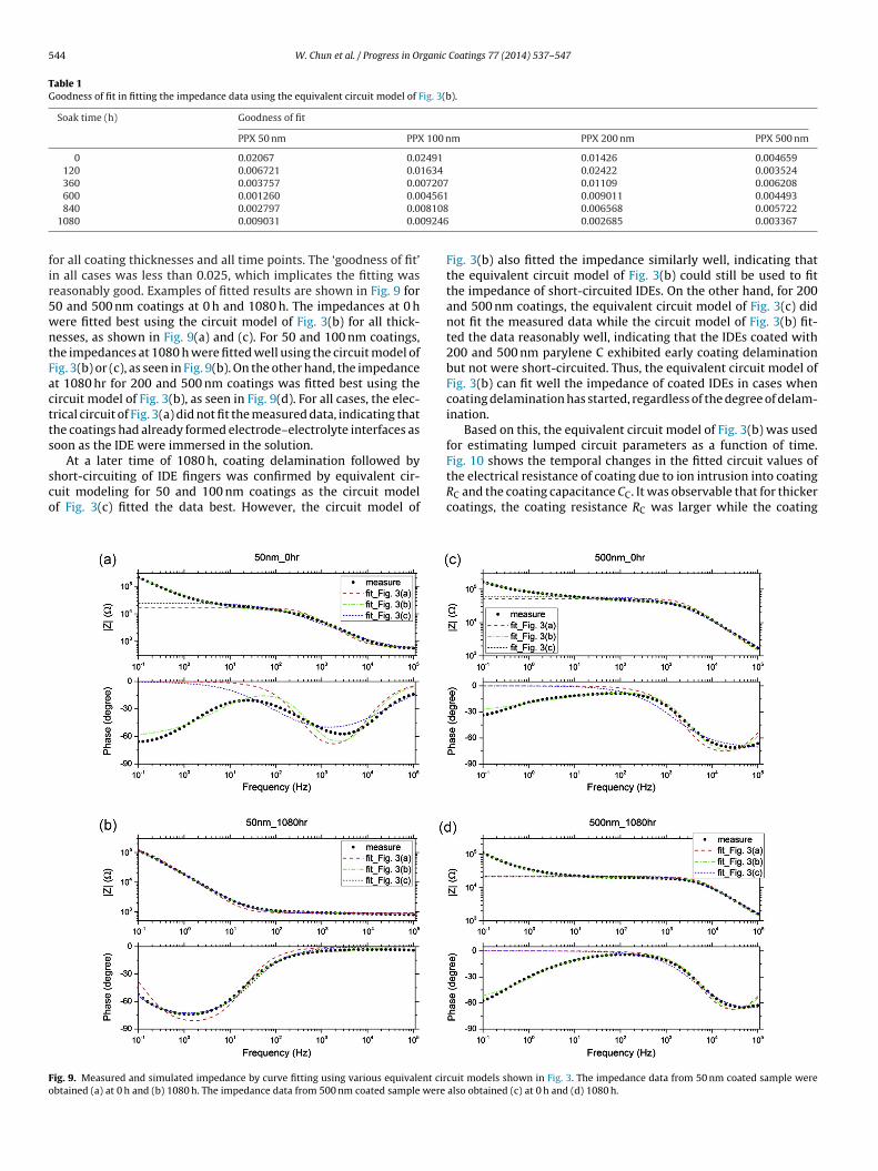
or all coating thicknesses and all time points. The ‘goodness of fit’n all cases was less than 0.025, which implicates the fitting waseasonably good. Examples of fitted results are shown in Fig. 9 for0 and 500 nm coatings at 0 h and 1080 h. The impedances at 0 here fitted best using the circuit model of Fig. 3(b) for all thick-esses, as shown in Fig. 9(a) and (c). For 50 and 100 nm coatings,he impedances at 1080 h were fitted well using the circuit model ofig. 3(b) or (c), as seen in Fig. 9(b). On the other hand, the impedancet 1080 hr for 200 and 500 nm coatings was fitted best using theircuit model of Fig. 3(b), as seen in Fig. 9(d). For all cases, the elec-rical circuit of Fig. 3(a) did not fit the measured data, indicating thathe coatings had already formed electrode–electrolyte interfaces asoon as the IDE were immersed in the solution.
At a later time of 1080 h, coating delamination followed by
hort-circuiting of IDE fingers was confirmed by equivalent cir-uit modeling for 50 and 100 nm coatings as the circuit modelf Fig. 3(c) fitted the data best. However, the circuit model ofig. 9. Measured and simulated impedance by curve fitting using various equivalent cirbtained (a) at 0 h and (b) 1080 h. The impedance data from 500 nm coated sample were
0.009011 0.004493 0.006568 0.005722
0.002685 0.003367
Fig. 3(b) also fitted the impedance similarly well, indicating thatthe equivalent circuit model of Fig. 3(b) could still be used to fitthe impedance of short-circuited IDEs. On the other hand, for 200and 500 nm coatings, the equivalent circuit model of Fig. 3(c) didnot fit the measured data while the circuit model of Fig. 3(b) fit-ted the data reasonably well, indicating that the IDEs coated with200 and 500 nm parylene C exhibited early coating delaminationbut not were short-circuited. Thus, the equivalent circuit model ofFig. 3(b) can fit well the impedance of coated IDEs in cases whencoating delamination has started, regardless of the degree of delam-ination.
Based on this, the equivalent circuit model of Fig. 3(b) was usedfor estimating lumped circuit parameters as a function of time.Fig. 10 shows the temporal changes in the fitted circuit values of
the electrical resistance of coating due to ion intrusion into coatingRC and the coating capacitance CC. It was observable that for thickercoatings, the coating resistance RC was larger while the coatingcuit models shown in Fig. 3. The impedance data from 50 nm coated sample werealso obtained (c) at 0 h and (d) 1080 h.
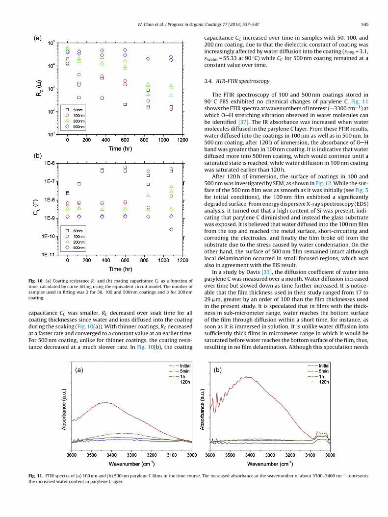
W. Chun et al. / Progress in Organic
Fig. 10. (a) Coating resistance RC and (b) coating capacitance CC as a function oftsc
ccdaFt
Ft
ime, calculated by curve fitting using the equivalent circuit model. The number ofamples used in fitting was 2 for 50, 100 and 500 nm coatings and 3 for 200 nmoating.
apacitance CC was smaller. RC decreased over soak time for alloating thicknesses since water and ions diffused into the coating
uring the soaking (Fig. 10(a)). With thinner coatings, RC decreasedt a faster rate and converged to a constant value at an earlier time.or 500 nm coating, unlike for thinner coatings, the coating resis-ance decreased at a much slower rate. In Fig. 10(b), the coatingig. 11. FTIR spectra of (a) 100 nm and (b) 500 nm parylene C films in the time course. The increased water content in parylene C layer.
Coatings 77 (2014) 537– 547 545
capacitance CC increased over time in samples with 50, 100, and200 nm coating, due to that the dielectric constant of coating wasincreasingly affected by water diffusion into the coating (εPPX = 3.1,εwater = 55.33 at 90 ◦C) while CC for 500 nm coating remained at aconstant value over time.
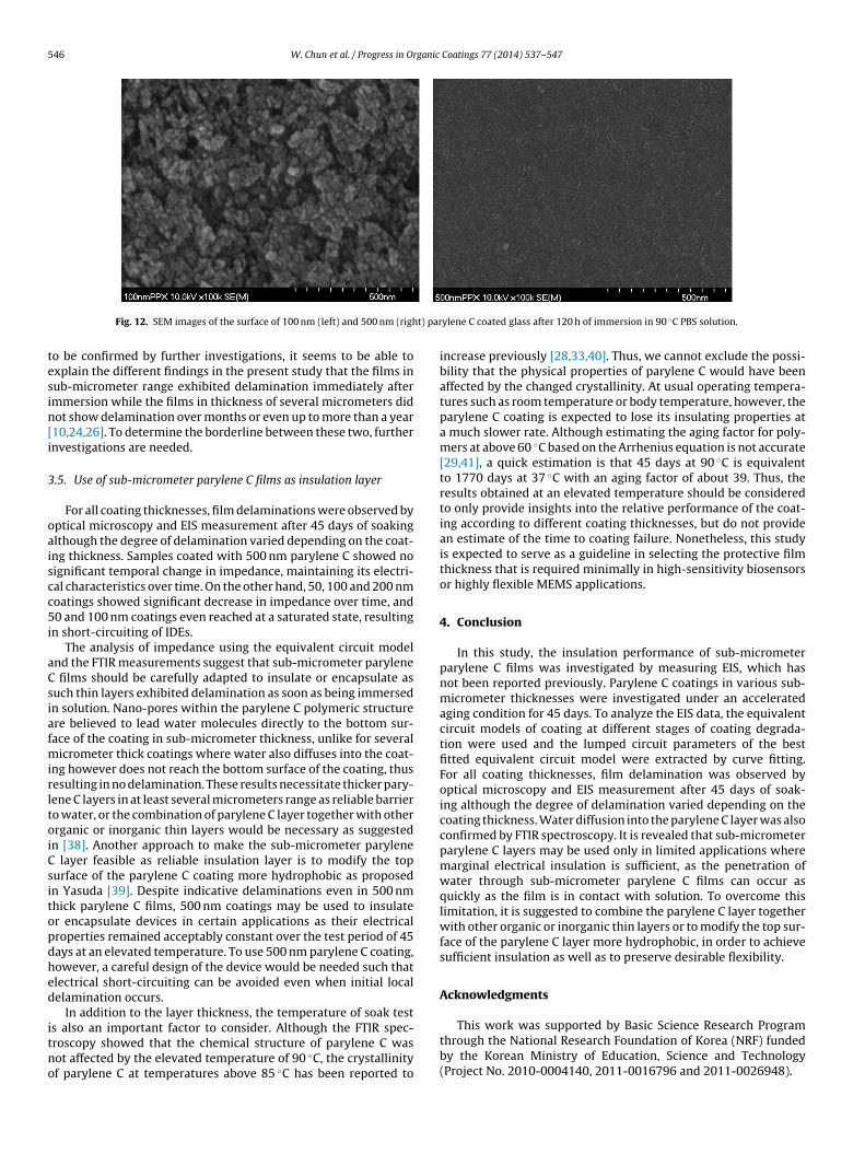
3.4. ATR-FTIR spectroscopy
The FTIR spectroscopy of 100 and 500 nm coatings stored in90 ◦C PBS exhibited no chemical changes of parylene C. Fig. 11shows the FTIR spectra at wavenumbers of interest (∼3300 cm−1) atwhich O H stretching vibration observed in water molecules canbe identified [37]. The IR absorbance was increased when watermolecules diffused in the parylene C layer. From these FTIR results,water diffused into the coatings in 100 nm as well as in 500 nm. In500 nm coating, after 120 h of immersion, the absorbance of O Hband was greater than in 100 nm coating. It is indicative that waterdiffused more into 500 nm coating, which would continue until asaturated state is reached, while water diffusion in 100 nm coatingwas saturated earlier than 120 h.
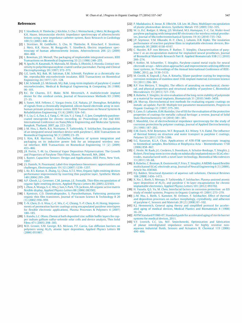
After 120 h of immersion, the surface of coatings in 100 and500 nm was investigated by SEM, as shown in Fig. 12. While the sur-face of the 500 nm film was as smooth as it was initially (see Fig. 5for initial conditions), the 100 nm film exhibited a significantlydegraded surface. From energy dispersive X-ray spectroscopy (EDS)analysis, it turned out that a high content of Si was present, indi-cating that parylene C diminished and instead the glass substratewas exposed. It is believed that water diffused into the 100 nm filmfrom the top and reached the metal surface, short-circuiting andcorroding the electrodes, and finally the film broke off from thesubstrate due to the stress caused by water condensation. On theother hand, the surface of 500 nm film remained intact althoughlocal delamination occurred in small focused regions, which wasalso in agreement with the EIS result.
In a study by Davis [33], the diffusion coefficient of water intoparylene C was measured over a month. Water diffusion increasedover time but slowed down as time further increased. It is notice-able that the film thickness used in their study ranged from 17 to29 �m, greater by an order of 100 than the film thicknesses usedin the present study. It is speculated that in films with the thick-ness in sub-micrometer range, water reaches the bottom surfaceof the film through diffusion within a short time, for instance, as
soon as it is immersed in solution. It is unlike water diffusion intosufficiently thick films in micrometer range in which it would besaturated before water reaches the bottom surface of the film, thus,resulting in no film delamination. Although this speculation needshe increased absorbance at the wavenumber of about 3300–3400 cm−1 represents
546 W. Chun et al. / Progress in Organic Coatings 77 (2014) 537– 547
t) par
tesin[i
3
oaiscc5i
aCsiafmirltoiCsitopdhed
itno
Fig. 12. SEM images of the surface of 100 nm (left) and 500 nm (righ
o be confirmed by further investigations, it seems to be able toxplain the different findings in the present study that the films inub-micrometer range exhibited delamination immediately aftermmersion while the films in thickness of several micrometers didot show delamination over months or even up to more than a year10,24,26]. To determine the borderline between these two, furthernvestigations are needed.
.5. Use of sub-micrometer parylene C films as insulation layer
For all coating thicknesses, film delaminations were observed byptical microscopy and EIS measurement after 45 days of soakinglthough the degree of delamination varied depending on the coat-ng thickness. Samples coated with 500 nm parylene C showed noignificant temporal change in impedance, maintaining its electri-al characteristics over time. On the other hand, 50, 100 and 200 nmoatings showed significant decrease in impedance over time, and0 and 100 nm coatings even reached at a saturated state, resulting
n short-circuiting of IDEs.The analysis of impedance using the equivalent circuit model
nd the FTIR measurements suggest that sub-micrometer parylene films should be carefully adapted to insulate or encapsulate asuch thin layers exhibited delamination as soon as being immersedn solution. Nano-pores within the parylene C polymeric structurere believed to lead water molecules directly to the bottom sur-ace of the coating in sub-micrometer thickness, unlike for several
icrometer thick coatings where water also diffuses into the coat-ng however does not reach the bottom surface of the coating, thusesulting in no delamination. These results necessitate thicker pary-ene C layers in at least several micrometers range as reliable barriero water, or the combination of parylene C layer together with otherrganic or inorganic thin layers would be necessary as suggestedn [38]. Another approach to make the sub-micrometer parylene
layer feasible as reliable insulation layer is to modify the topurface of the parylene C coating more hydrophobic as proposedn Yasuda [39]. Despite indicative delaminations even in 500 nmhick parylene C films, 500 nm coatings may be used to insulater encapsulate devices in certain applications as their electricalroperties remained acceptably constant over the test period of 45ays at an elevated temperature. To use 500 nm parylene C coating,owever, a careful design of the device would be needed such thatlectrical short-circuiting can be avoided even when initial localelamination occurs.
In addition to the layer thickness, the temperature of soak test
s also an important factor to consider. Although the FTIR spec-roscopy showed that the chemical structure of parylene C wasot affected by the elevated temperature of 90 ◦C, the crystallinityf parylene C at temperatures above 85 ◦C has been reported toylene C coated glass after 120 h of immersion in 90 ◦C PBS solution.
increase previously [28,33,40]. Thus, we cannot exclude the possi-bility that the physical properties of parylene C would have beenaffected by the changed crystallinity. At usual operating tempera-tures such as room temperature or body temperature, however, theparylene C coating is expected to lose its insulating properties ata much slower rate. Although estimating the aging factor for poly-mers at above 60 ◦C based on the Arrhenius equation is not accurate[29,41], a quick estimation is that 45 days at 90 ◦C is equivalentto 1770 days at 37 ◦C with an aging factor of about 39. Thus, theresults obtained at an elevated temperature should be consideredto only provide insights into the relative performance of the coat-ing according to different coating thicknesses, but do not providean estimate of the time to coating failure. Nonetheless, this studyis expected to serve as a guideline in selecting the protective filmthickness that is required minimally in high-sensitivity biosensorsor highly flexible MEMS applications.
4. Conclusion
In this study, the insulation performance of sub-micrometerparylene C films was investigated by measuring EIS, which hasnot been reported previously. Parylene C coatings in various sub-micrometer thicknesses were investigated under an acceleratedaging condition for 45 days. To analyze the EIS data, the equivalentcircuit models of coating at different stages of coating degrada-tion were used and the lumped circuit parameters of the bestfitted equivalent circuit model were extracted by curve fitting.For all coating thicknesses, film delamination was observed byoptical microscopy and EIS measurement after 45 days of soak-ing although the degree of delamination varied depending on thecoating thickness. Water diffusion into the parylene C layer was alsoconfirmed by FTIR spectroscopy. It is revealed that sub-micrometerparylene C layers may be used only in limited applications wheremarginal electrical insulation is sufficient, as the penetration ofwater through sub-micrometer parylene C films can occur asquickly as the film is in contact with solution. To overcome thislimitation, it is suggested to combine the parylene C layer togetherwith other organic or inorganic thin layers or to modify the top sur-face of the parylene C layer more hydrophobic, in order to achievesufficient insulation as well as to preserve desirable flexibility.
Acknowledgments
This work was supported by Basic Science Research Programthrough the National Research Foundation of Korea (NRF) fundedby the Korean Ministry of Education, Science and Technology(Project No. 2010-0004140, 2011-0016796 and 2011-0026948).
ganic
R
[
[
[
[
[
[
[
[
[
[
[
[
[
[
[
[
[
[
[
[
[
[
[
[
[
[
[
[
[
[
[
[
[
W. Chun et al. / Progress in Or
eferences
[1] T. Süselbeck, H. Thielecke, J. Köchlin, S. Cho, I. Weinschenk, J. Metz, M. Borggrefe,K.K. Haase, Intravascular electric impedance spectroscopy of atheroscleroticlesions using a new impedance catheter system, Basic Research in Cardiology100 (5) (2005) 446–452.
[2] I. Streitner, M. Goldhofer, S. Cho, H. Thielecke, R. Kinscherf, F. Streitner,J. Metz, K.K. Hasse, M. Borggrefe, T. Süselbeck, Electric impedance spec-troscopy of human atherosclerotic lesions, Atherosclerosis 206 (2) (2009)464–468.
[3] L. Bowman, J.D. Meindl, The packaging of implantable integrated sensors, IEEETransactions on Biomedical Engineering 33 (2) (1986) 248–255.
[4] N. Iguchi, H. Kasanuki, N. Matsuda, M. Shoda, S. Ohnishi, S. Hosoda, Contact sen-sitivity to polychloroparaxylene-coated cardiac pacemaker, Pacing and ClinicalElectrophysiology 20 (1997) 372–373.
[5] G.E. Loeb, M.J. Bak, M. Salcman, E.M. Schmidt, Parylene as a chronically sta-ble, reproducible microelectrode insulator, IEEE Transactions on BiomedicalEngineering 24 (1977) 121–128.
[6] E.M. Schmidt, J.S. McIntosh, M.J. Bak, Long-term implants of parylene-C coatedmicroelectrodes, Medical & Biological Engineering & Computing 26 (1988)96–101.
[7] R.C. De Charms, D.T. Blake, M.M. Merzenich, A multielectrode implantdevice for the cerebral cortex, Journal of Neuroscience Methods 93 (1999)27–35.
[8] S. Suner, M.R. Fellows, C. Vargas-Irwin, G.K. Nakata, J.P. Donoghue, Reliabilityof signals from a chronically implanted, silicon-based electrode array in non-human primate primary motor cortex, IEEE Transactions on Neural Systems &Rehabilitation Engineering 13 (4) (2005) 524–541.
[9] P.-L. Lu, C.-L. Fan, L.-J. Yang, C.-W. Lin, Y.-J. Yang, F.-S. Jaw, Completely parylene-coated neuroprobe for chronic recording, in: Proceedings of the 2nd IEEEInternational Conference on Nano/Micro Engineering and Molecular Systems,Bangkok, Thailand, 2007, pp. 223–226.
10] J.-M. Hsu, L. Rieth, R.A. Normann, P. Tathireddy, F. Solzbacher, Encapsulationof an integrated neural interface device with parylene C, IEEE Transactions onBiomedical Engineering 56 (1) (2009) 23–29.
11] S. Kim, R.R. Harrison, F. Solzbacher, Influence of system integration andpackaging on its inductive power link for an integrated wireless neu-ral interface, IEEE Transactions on Biomedical Engineering 11 (2) (2009)453–466.
12] J.B. Fortin, T.-M. Lu, Chemical Vapor Deposition Polymerization: The Growthand Properties of Parylene Thin Films, Kluwer, Norwell, MA, 2004.
13] L. Baxter, Capacitive Sensors: Design and Applications, IEEE Press, New York,1997.
14] J.S. Daniels, N. Pourmand, Label-free impedance biosensors: opportunities andchallenges, Electroanalysis 19 (12) (2007) 1239–1257.
15] L. Ke, R.S. Kumar, K. Zhang, S.J. Chua, A.T.S. Wee, Organic light emitting devicesperformance improvement by inserting thin parylene layer, Synthetic Metals140 (2004) 295–299.
16] A.P. Ghosh, L.J. Gerenser, C.M. Jarman, J.E. Fornalik, Thin-film encapsulation oforganic light-emitting devices, Applied Physics Letters 86 (2005) 223503.
17] L. Zhou, A. Wanga, S.-C. Wu, J. Sun, S. Park, T.N. Jackson, All-organic active matrixflexible display, Applied Physics Letters 88 (2006) 083502.
18] I. Kymissis, C.D. Dimitrakopoulos, S. Purushothaman, Patterning pentaceneorganic thin film transistors, Journal of Vacuum Science & Technology B 20(3) (2002) 956–959.
19] T.-N. Chen, D.-S. Wuu, C.-C. Wu, C.-C. Chiang, Y.-P. Chen, R.-H. Horng, Improve-ments of permeation barrier coatings using encapsulated parylene interlayersfor flexible electronic applications, Plasma Processes & Polymers 4 (2007)180–185.
20] S. Kundu, L.C. Olsen, Chemical bath deposited zinc sulfide buffer layers for cop-
per indium gallium sulfur-selenide solar cells and device analysis, Thin SolidFilms 471 (2005) 298–303.21] M.D. Groner, S.M. George, R.S. McLean, P.F. Carcia, Gas diffusion barriers onpolymers using Al2O3 atomic layer deposition, Applied Physics Letters 88(2006) 051907.
[
Coatings 77 (2014) 537– 547 547
22] P. Madakasira, K. Inoue, R. Ulbricht, S.B. Lee, M. Zhou, Multilayer encapsulationof plastic photovoltaic devices, Synthetic Metals 155 (2005) 332–335.
23] W. Li, D.C. Rodger, E. Meng, J.D. Weiland, M.S. Humayun, Y.-C. Tai, Wafer-levelparylene packaging with integrated RF electronics for wireless retinal prosthe-ses, Journal of Microelectromechanical Systems 19 (4) (2010) 735–742.
24] J.P. Seymour, Y.M. Elkasabi, H.-Y. Chen, J. Lahann, D.R. Kipke, The insulationperformance of reactive parylene films in implantable electronic devices, Bio-materials 30 (2009) 6158–6167.
25] C. Hassler, R.P. von Metzen, P. Ruther, T. Stieglitz, Characterization of pary-lene C as an encapsulation material for implanted neural prostheses, Journalof Biomedical Materials Research Part B: Applied Biomaterials 93B (1) (2010)266–274.
26] F. Kohler, M. Schuettler, T. Stieglitz, Parylene-coated metal tracks for neuralelectrode arrays – fabrication approaches and improvements utilizing differentlaser systems, in: Proceedings of the Annual International Conference of IEEE-EMBC, 2012, pp. 5130–5133.
27] M. Cieslik, K. Engvall, J. Pan, A. Kotarba, Silane-parylene coating for improvingcorrosion resistance of stainless steel 316L implant material, Corrosion Science53 (2011) 296–301.
28] R.P. Von Metzen, T. Stieglitz, The effects of annealing on mechanical, chemi-cal, and physical properties and structural stability of parylene C, BiomedicalMicrodevices 15 (2013) 727–735.
29] B. Rubehn, T. Stieglitz, In vitro evaluation of the long-term stability of polyimideas a material for neural implants, Biomaterials 31 (2010) 3449–3458.
30] J.N. Murray, Electrochemical test methods for evaluating organic coatings onmetals: an update. Part III: Multiple test parameter measurements, Progress inOrganic Coatings 31 (1997) 375–391.
31] E. Cano, D. Lafuente, D.M. Bastidas, Use of EIS for the evaluation of the protectiveproperties of coatings for metallic cultural heritage: a review, Journal of SolidState Electrochemistry 14 (2010) 381–391.
32] F. Mansfeld, Use of electrochemical impedance spectroscopy for the study ofcorrosion protection by polymer coatings, Journal of Applied Electrochemistry25 (1995) 187–202.
33] E.M. Davis, N.M. Benetatos, W.F. Regnault, K.I. Winey, Y.A. Elabd, The influenceof thermal history on structure and water transport in parylene C coatings,Polymer 52 (2011) 5378–5386.
34] S.G. Kazarian, K.L.A. Chan, Applications of ATR-FTIR spectroscopic imagingto biomedical samples, Biochimica et Biophysica Acta – Biomembranes 1758(2006) 858–867.
35] C. Henle, M. Raab, J.G. Cordeiro, S. Doostkam, A. Schulze-Bonhage, T. Stieglitz, J.Rickert, First long-term in vivo study on subdurally implanted micro-ECoG elec-trodes, manufactured with a novel laser technology, Biomedical Microdevices13 (2011) 59–68.
36] B. Rubehn, C. Bosman, R. Oostenveld, P. Fries, T. Stieglitz, A MEMS-based flexiblemultichannel ECoG-electrode array, Journal of Neural Engineering 6 (3) (2009),Article No. 030360.
37] H.J. Bakker, Structural dynamics of aqueous salt solutions, Chemical Reviews108 (2008) 1456–1473.
38] X. Xie, L. Rieth, S. Merugu, P. Tathireddy, F. Solzbacher, Plasma-assisted atomiclayer deposition of Al2O3 and parylene C bi-layer encapsulation for chronicimplantable electronics, Applied Physics Letters 101 (2012) 093702.
39] H. Yasuda, Q.S. Yu, M. Chen, Interfacial factors in corrosion protection: an EISstudy of model systems, Progress in Organic Coatings 41 (2001) 273–279.
40] J.-M. Hsu, L. Rieth, S. Kammer, M. Orthner, F. Solzbacher, Effect of thermaland deposition processes on surface morphology, crystallinity, and adhesionof parylene-C, Sensors and Materials 20 (2) (2008) 87–102.
41] K.J. Hemmerich, General aging theory and simplified protocol for acceler-ated aging of medical devices, Medical Plastics and Biomaterials 4 (1998)16–24.
42] ASTM Standard F1980-07, Standard guide for accelerated aging of sterile barrier
systems for medical devices, 2011.43] V.F. Lvovich, C.C. Liu, M.F. Smiechowski, Optimization and fabricationof planar interdigitated impedance sensors for highly resistive non-aqueous industrial fluids, Sensors and Actuators B: Chemical 119 (2006)490–496.