Embed Size (px)
Citation preview
Rev. 1.0
Data Sheet
Fastrax IT530
This document describes the electrical connectivity and functionality of the Fastrax IT530 OEM
GPS Receiver.
December 19, 2011
Fastrax Ltd
Page 2 of 35
2011-12-19 IT530_Datasheet
TRADEMARKS
Fastrax is a registered trademark of Fastrax Ltd.
All other trademarks are trademarks of MediaTek, Inc. or either of respective holders.
COPYRIGHT
© 2011 Fastrax Ltd
DISCLAIMER
This document is compiled and kept up-to-date as conscientiously as possible. Fastrax Ltd cannot, however,
guarantee that the data are free of errors, accurate or complete and, therefore, assumes no liability for loss or
damage of any kind incurred directly or indirectly through the use of this document. The information in this
document is subject to change without notice and describes only generally the product defined in the introduction
of this documentation. Fastrax products are not authorized for use in life-support or safety-critical applications.
Use in such applications is done at the sole discretion of the customer. Fastrax will not warrant the use of its
devices in such applications.
REFERENCES
Ref. # Publisher; Reference
(1) Fastrax; NMEA Manual for Fastrax IT500 Series GPS receivers
(2) Fastrax; Reflow_soldering_ profile.pdf
Page 3 of 35
2011-12-19 IT530_Datasheet
CHANGE LOG
Rev. Notes Date
1.0 Initial documentation 2011-12-19
Page 4 of 35
2011-12-19 IT530_Datasheet
1 Contents 2 Overview .............................................................................................................................................................. 6
2.1 General ........................................................................................................................................................ 6
2.2 Block diagram .............................................................................................................................................. 7
2.3 Frequency Plan ............................................................................................................................................ 7
2.4 General Specifications ................................................................................................................................. 7
3 Operation ............................................................................................................................................................. 9
3.1 Operating Modes ........................................................................................................................................ 9
3.2 Full Power Mode ......................................................................................................................................... 9
3.2.1 Host port configuration .......................................................................................................................... 9
3.3 Power Management Modes ........................................................................................................................ 9
3.4 Self-Assistance EASY™ usage..................................................................................................................... 11
3.5 Server Assistance EPO™ usage .................................................................................................................. 11
3.6 Logger LOCUS usage .................................................................................................................................. 11
3.7 DGPS usage ............................................................................................................................................... 11
3.8 Standby Mode ........................................................................................................................................... 11
3.9 Backup State.............................................................................................................................................. 12
3.10 Reset State ................................................................................................................................................ 12
4 Connectivity ....................................................................................................................................................... 13
4.1 Signal Assignments .................................................................................................................................... 13
4.2 Power supply ............................................................................................................................................. 14
4.3 Host port configuration ............................................................................................................................. 15
4.4 Host port UART ......................................................................................................................................... 15
4.5 Reset input ................................................................................................................................................ 15
4.6 Timer output ............................................................................................................................................. 15
4.7 Antenna input ........................................................................................................................................... 15
4.8 Active GPS antenna ................................................................................................................................... 16
4.8.1 Jamming Remover ................................................................................................................................ 16
4.9 PPS output ................................................................................................................................................. 17
4.10 Wakeup output ......................................................................................................................................... 17
4.11 Interrupt input EINT1 ................................................................................................................................ 17
4.12 UI_FIX signal .............................................................................................................................................. 17
4.13 32K/DR_INT signal ..................................................................................................................................... 17
4.14 Mechanical Dimensions ............................................................................................................................ 18
4.15 Suggested pad layout ................................................................................................................................ 19
5 Electrical Specifications ...................................................................................................................................... 20
Page 5 of 35
2011-12-19 IT530_Datasheet
5.1 Absolute Maximum Ratings ...................................................................................................................... 20
5.2 DC Electrical specifications ........................................................................................................................ 20
5.3 AC Electrical characteristics ...................................................................................................................... 21
6 Manufacturing ................................................................................................................................................... 22
6.1 Assembly and Soldering ............................................................................................................................ 22
6.2 Moisture sensitivity ................................................................................................................................... 22
6.3 Marking ..................................................................................................................................................... 22
6.4 Tape and reel ............................................................................................................................................ 23
6.5 Environmental Specification ..................................................................................................................... 23
7 Reference design ............................................................................................................................................... 24
7.1 Reference circuit diagram ......................................................................................................................... 24
7.2 PCB layout suggestion ............................................................................................................................... 26
7.2.1 Other electronics on mother board ...................................................................................................... 26
7.2.2 Avoiding EMI ......................................................................................................................................... 27
8 AP530 Application board for IT530 .................................................................................................................... 28
8.1 Board Terminal I/O-connector .................................................................................................................. 28
8.2 Bill of materials ......................................................................................................................................... 29
8.3 AP530 Circuit diagram ............................................................................................................................... 31
8.4 AP530 layout and assembly ...................................................................................................................... 32
Page 6 of 35
2011-12-19 IT530_Datasheet
2 Overview
2.1 General The Fastrax IT530 is an OEM GPS receiver module with the Mediatek MT3339 receiver. The module has ultra small
form factor 9.6x9.6 mm, height is 1.85 mm nominal (2.15 mm max) and can be assembled with SMT reflow
soldering. The Fastrax IT530 receiver provides extremely low power and very fast TTFF together with weak signal
acquisition and tracking capability to meet even the most stringent performance expectations.
The IT530 provides complete signal processing from antenna input to host port UART and location data output is
in NMEA protocol. The module requires a main and a backup power supply. The host port is configurable to UART
during power up. Host data and I/O signal levels are 2.8V CMOS compatible and inputs are 3.6V tolerable.
The IT530 supports a new feature called AlwaysLocate™, which is an intelligent controller of the IT530 power
saving mode. Depending on the environment and motion conditions, the module can adaptively adjust the
navigation activity in order to achieve a balance in positioning accuracy, fix rate and power consumption; typical
power consumption varies between 2… 8 mW.
The module is also optionally self-assisted since the EASY™ (Embedded Assist System) ephemeris extension is
embedded in the software without any resources required from the host. The EASY™ data is stored on internal
flash memory and allows fast TTFF typ. 3 seconds over 3 days. Also EPO™ (Extended Prediction Orbit) server
generated extended ephemeris input is also supported, which allows fast TTFF 10 seconds typ. over 7/14 days.
The IT530 contains also an AIC (Active Interference Cancellation), which provides state-of-art narrow band (CW)
interference and jamming elimination up to 12 CW jammers < -80dBm.
The module also supports a logging feature called LOCUS, which enables automatic logging of position data to
internal flash memory. The logging capacity is >16 hrs typ. @ 15 sec storage interval.
The antenna input supports passive and active antennas with excellent out-of-band blocking rejection and
provides also an input for externally generated antenna bias supply.
This document describes the electrical connectivity and main functionality of the Fastrax IT530 OEM GPS Receiver
module.
Page 7 of 35
2011-12-19 IT530_Datasheet
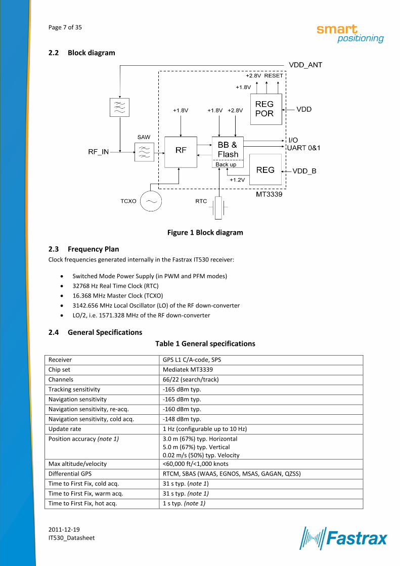
2.2 Block diagram
Figure 1 Block diagram
2.3 Frequency Plan Clock frequencies generated internally in the Fastrax IT530 receiver:
Switched Mode Power Supply (in PWM and PFM modes)
32768 Hz Real Time Clock (RTC)
16.368 MHz Master Clock (TCXO)
3142.656 MHz Local Oscillator (LO) of the RF down-converter
LO/2, i.e. 1571.328 MHz of the RF down-converter
2.4 General Specifications
Table 1 General specifications
Receiver GPS L1 C/A-code, SPS
Chip set Mediatek MT3339
Channels 66/22 (search/track)
Tracking sensitivity -165 dBm typ.
Navigation sensitivity -165 dBm typ.
Navigation sensitivity, re-acq. -160 dBm typ.
Navigation sensitivity, cold acq. -148 dBm typ.
Update rate 1 Hz (configurable up to 10 Hz)
Position accuracy (note 1) 3.0 m (67%) typ. Horizontal 5.0 m (67%) typ. Vertical 0.02 m/s (50%) typ. Velocity
Max altitude/velocity <60,000 ft/<1,000 knots
Differential GPS RTCM, SBAS (WAAS, EGNOS, MSAS, GAGAN, QZSS)
Time to First Fix, cold acq. 31 s typ. (note 1)
Time to First Fix, warm acq. 31 s typ. (note 1)
Time to First Fix, hot acq. 1 s typ. (note 1)
Page 8 of 35
2011-12-19 IT530_Datasheet
Supply voltage, main VDD +3.0 … +4.3 V
Supply voltage, backup VDD_B +2.0 … +4.3 V
Power consumption, Full Power 35 mW typ. @ 3.3 V (note 2)
Power consumption, AlwaysLocate™ 3 mW typ. @ 3.3 V
Power consumption, Backup state 15 µW typ. @ 3.0 V
External RF amplifier net gain range 0… +30 dB
Storage temperature -40°C…+85°C
Operating temperature -40°C…+85°C (note 3)
Host port configuration UART
Host port protocol NMEA-0183 rev. 3.01
Serial data format (UART) 8 bits, no parity, 1 stop bit
Serial data speed (UART) 9600 baud (configurable 4,800... 921,600 baud)
PPS output 100 ms high pulse, rising edge +/-1 µs @ full second GPS epoch
Note 1: With nominal GPS signal levels -130dBm.
Note 2: @ 1Hz navigation, <12 GPS satellites in track, SBAS disabled, average over 24h
Note 3: Operation in the temperature range –40°C… –30°C is allowed but Time-to-First-Fix performance
and tracking sensitivity may be degraded.
Page 9 of 35
2011-12-19 IT530_Datasheet
3 Operation
3.1 Operating Modes
After power up the IT530 module boots from the internal ROM to Navigation Mode. Modes of operation:
Navigation Mode (Full Power) o Power management system modes
Standby Mode Backup State/Mode Reset State
3.2 Full Power Mode The module will enter Full Power (aka Navigation Mode) after first power up with factory configuration settings.
Power consumption will vary depending on the amount of satellite acquisitions and number of satellites in track.
This Mode is also referenced as Full On, Full Power or Navigation Mode.
Navigation is available and any configuration settings are valid as long as the main VDD and backup VDD_B power
supplies are active. When the main VDD and backup VDD_B supply is powered off, settings are reset to factory
configuration and receiver performs a cold start on next power up.
Suggestion is to keep the backup supply VDD_B active all the time in order to sustain on time, position and
ephemeris in the backup RTC and RAM. The main VDD supply can be used to control the module activity, i.e. when
VDD is switched off, the module operation is stopped.
Navigation fix rate can be configured by a NMEA command, see chapter 0. Note that baud rate must be set high
enough or message payload low enough in order to pass through all messages pending.
3.2.1 Host port configuration Default host port is configured to UART Port 0 by keeping GPIO9 and GPIO10 floating (not connected) during
power up. UART Port1 is reserved for DGPS/RTCM protocol.
Default protocol for host communication is NMEA at 9600 baud. Details on NMEA protocol can be found in NMEA
manual, ref (1). Default NMEA message output configuration: $GPGGA, $GPGSA, $GPGSV, $GPRMC and $GPVTG
rate every second. The module supports also proprietary $PMTK input commands, see ref (1). The message
payload consists of $PMTK<cmd_id>,<data_field(s)>*<chk_sum><CR><LF>. Sample command:
$PMTK000*32<CR><LF>. For clarity <CR><LF> are not displayed in the following example messages but should be
added to the payload at host.
3.3 Power Management Modes
The IT530 module supports also low power operating modes for reduced power consumption:
1. Standby Mode: In this Mode the receiver stops navigation and internal processor enters standby state; current drain at main supply VDD is reduced to 200 µA typ. Standby Mode is entered by sending NMEA command: $PMTK161,0*28. Host can wake up the module from Standby Mode to Full Power Mode by sending any byte via host port.
2. Backup Mode: In this mode the receiver is configured to wake up autonomously after elapsed time or after a host/sensor interrupt via 32K/DR_INT signal; the main power supply VDD is controlled on/off externally by a power switch that is controlled by the TIMER signal output, see reference circuit in chapter 7.1. Rest of the time the receiver stays in Backup state (backup supply VDD_B active) while VDD supply is switched off. Backup Mode is entered by sending NMEA command: $PMTK291,7,<Sensor_En>,<RTCWakeup>,1*<checksum><CR><LF>, where Sensor_En=0: Disable sensor
Page 10 of 35
2011-12-19 IT530_Datasheet
wakeup; Sensor_En=1: Enable host/sensor wakeup via 32K/DR_INT signal; RTCWakeup = wakeup after elapsed time (ms), max 518,400,000 (6 days). Example: $PMTK291,7,0,10000,1*3F for 10 sec Backup state without sensor wakeup.
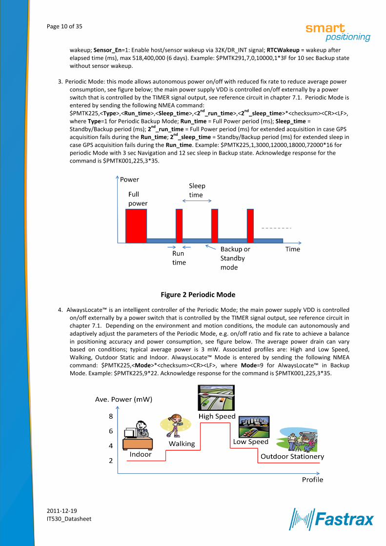
3. Periodic Mode: this mode allows autonomous power on/off with reduced fix rate to reduce average power consumption, see figure below; the main power supply VDD is controlled on/off externally by a power switch that is controlled by the TIMER signal output, see reference circuit in chapter 7.1. Periodic Mode is entered by sending the following NMEA command: $PMTK225,<Type>,<Run_time>,<Sleep_time>,<2
nd_run_time>,<2
nd_sleep_time>*<checksum><CR><LF>,
where Type=1 for Periodic Backup Mode; Run_time = Full Power period (ms); Sleep_time = Standby/Backup period (ms); 2
nd_run_time = Full Power period (ms) for extended acquisition in case GPS
acquisition fails during the Run_time; 2nd
_sleep_time = Standby/Backup period (ms) for extended sleep in case GPS acquisition fails during the Run_time. Example: $PMTK225,1,3000,12000,18000,72000*16 for periodic Mode with 3 sec Navigation and 12 sec sleep in Backup state. Acknowledge response for the command is $PMTK001,225,3*35.
Figure 2 Periodic Mode
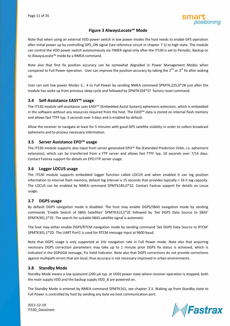
4. AlwaysLocate™ is an intelligent controller of the Periodic Mode; the main power supply VDD is controlled on/off externally by a power switch that is controlled by the TIMER signal output, see reference circuit in chapter 7.1. Depending on the environment and motion conditions, the module can autonomously and adaptively adjust the parameters of the Periodic Mode, e.g. on/off ratio and fix rate to achieve a balance in positioning accuracy and power consumption, see figure below. The average power drain can vary based on conditions; typical average power is 3 mW. Associated profiles are: High and Low Speed, Walking, Outdoor Static and Indoor. AlwaysLocate™ Mode is entered by sending the following NMEA command: $PMTK225,<Mode>*<checksum><CR><LF>, where Mode=9 for AlwaysLocate™ in Backup Mode. Example: $PMTK225,9*22. Acknowledge response for the command is $PMTK001,225,3*35.
Page 11 of 35
2011-12-19 IT530_Datasheet
Figure 3 AlwaysLocate™ Mode
Note that when using an external VDD power switch in low power modes the host needs to enable GPS operation
after initial power up by controlling GPS_ON signal (see reference circuit in chapter 7.1) to high state. The module
can control the VDD power switch autonomously via TIMER signal only after the IT530 is set to Periodic, Backup or
to AlwaysLocate™ mode by a NMEA command.
Note also that first fix position accuracy can be somewhat degraded in Power Management Modes when
compared to Full Power operation. User can improve the position accuracy by taking the 2nd
or 3rd
fix after waking
up.
User can exit low power Modes 3… 4 to Full Power by sending NMEA command $PMTK,225,0*2B just after the
module has woke up from previous sleep cycle and followed by $PMTK104*37 factory reset command.
3.4 Self-Assistance EASY™ usage The IT530 module self-assistance uses EASY™ (Embedded Assist System) ephemeris extension, which is embedded
in the software without any resources required from the host. The EASY™ data is stored on internal flash memory
and allows fast TTFF typ. 3 seconds over 3 days and is enabled by default.
Allow the receiver to navigate at least for 5 minutes with good GPS satellite visibility in order to collect broadcast
ephemeris and to process necessary information.
3.5 Server Assistance EPO™ usage The IT530 module supports also input from server generated EPO™ file (Extended Prediction Orbit, i.e. ephemeris
extension), which can be transferred from a FTP server and allows fast TTFF typ. 10 seconds over 7/14 days.
Contact Fastrax support for details on EPO FTP server usage.
3.6 Logger LOCUS usage The IT530 module supports embedded logger function called LOCUS and when enabled it can log position
information to internal flash memory; default log interval is 15 seconds that provides typically > 16 h log capacity.
The LOCUS can be enabled by NMEA command $PMTK185,0*22. Contact Fastrax support for details on Locus
usage.
3.7 DGPS usage By default DGPS navigation mode is disabled. The host may enable DGPS/SBAS navigation mode by sending
commands ‘Enable Search of SBAS Satellites’ $PMTK313,1*2E followed by ‘Set DGPS Data Source to SBAS’
$PMTK301,2*2E. The search for suitable SBAS satellite signal is automatic.
The host may either enable DGPS/RTCM navigation mode by sending command ‘Set DGPS Data Source to RTCM’
$PMTK301,1*2D. The UART Port1 is used for RTCM message input at 9600 baud.
Note that DGPS usage is only supported at 1Hz navigation rate in Full Power mode. Note also that acquiring
necessary DGPS correction parameters may take up to 1 minute prior DGPS fix status is achieved, which is
indicated in the $GPGGA message, Fix Valid Indicator. Note also that DGPS corrections do not provide corrections
against multipath errors that are local; thus accuracy is not necessary improved in urban environments.
3.8 Standby Mode Standby Mode means a low quiescent (200 µA typ. at VDD) power state where receiver operation is stopped; both
the main supply VDD and the backup supply VDD_B are powered on.
The Standby Mode is entered by NMEA command $PMTK161, see chapter 3.3. Waking up from Standby state to
Full Power is controlled by host by sending any byte via host communication port.
Page 12 of 35
2011-12-19 IT530_Datasheet
After waking up the receiver will use all internal aiding like GPS time, Ephemeris, Last Position etc. resulting to a
fastest possible TTFF in either Hot or Warm start Modes.
3.9 Backup State Backup State means a low quiescent (5 µA typ. at VDD_B) power state where receiver operation is stopped; only
the backup supply VDD_B is powered on while the main supply VDD is switched off by host or by IT530, see also
chapter 3.3. Waking up from Backup State to Full Power is controlled by host by switching on the VDD supply.
In optional Autonomous Backup Mode the IT530 module controls the VDD switching autonomously via the TIMER
signal, see reference circuit in chapter 7.1 by sending NMEA command $PMTK291, see chapter 3.3. The
Autonomous Backup Mode is thus similar to Backup State but with autonomous control of external VDD power
switch.
Note that when using an external VDD power switch in low power modes the host needs to enable GPS operation
after initial power up by controlling GPS_ON signal (see reference circuit in chapter 7.1) to high state. The module
can control the VDD power switch autonomously via TIMER signal only after the IT530 is set to Periodic, Backup or
to AlwaysLocate™ mode by a NMEA command.
After waking up the receiver will use all internal aiding like GPS time, Ephemeris, Last Position etc. resulting to a
fastest possible TTFF in either Hot or Warm start modes.
During Autonomous Backup Mode or Backup State the I/O block is powered off; thus suggestion is that host shall
force it’s outputs to low state or to high-Z state during Backup state to minimize small leakage currents (<10 µA
typ.) at receiver’s input signals.
3.10 Reset State Reset State stops all internal operations and it is entered internally at power up after which internal reset state is
relaxed when 167 ms (typ.) has elapsed and module operations begin. The power on reset level is 2.7 +/- 0.1 V at
VDD. Host can also override Reset State via RESET_N input, which is low state active. Normally external reset
override is not required and RESET_N signal can be left floating (not connected).
Page 13 of 35
2011-12-19 IT530_Datasheet
4 Connectivity
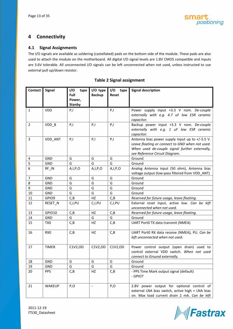
4.1 Signal Assignments The I/O signals are available as soldering (castellated) pads on the bottom side of the module. These pads are also
used to attach the module on the motherboard. All digital I/O signal levels are 1.8V CMOS compatible and inputs
are 3.6V tolerable. All unconnected I/O signals can be left unconnected when not used, unless instructed to use
external pull up/down resistor.
Table 2 Signal assignment
Contact Signal I/O type Full Power, Stanby
I/O type Backup
I/O type Reset
Signal description
1 VDD P,I - P,I Power supply input +3.3 V nom. De-couple externally with e.g. 4.7 uF low ESR ceramic capacitor.
2 VDD_B P,I P,I P,I Backup power input +3.3 V nom. De-couple externally with e.g. 1 uF low ESR ceramic capacitor.
3 VDD_ANT P,I P,I P,I Antenna bias power supply input up to +/-5.5 V. Leave floating or connect to GND when not used. When used de-couple signal further externally, see Reference Circuit Diagram.
4 GND G G G Ground
5 GND G G G Ground
6 RF_IN A,I,P,O A,I,P,O A,I,P,O Analog Antenna input (50 ohm), Antenna bias voltage output (low-pass filtered from VDD_ANT)
7 GND G G G Ground
8 GND G G G Ground
9 GND G G G Ground
10 GND G G G Ground
11 GPIO9 C,B HZ C,B Reserved for future usage, leave floating.
12 RESET_N C,I,PU C,I,PU C,I,PU External reset input, active low. Can be left unconnected when not used.
13 GPIO10 C,B HZ C,B Reserved for future usage, leave floating.
14 GND G G G Ground
15 TX0 C,B HZ C,B UART Port0 TX data transmit (NMEA)
16 RX0 C,B HZ C,B UART Port0 RX data receive (NMEA), PU. Can be left unconnected when not used.
17 TIMER C1V2,OD C1V2,OD C1V2,OD Power control output (open drain) used to control external VDD switch. When not used connect to Ground externally.
18 GND G G G Ground
19 GND G G G Ground
20 PPS C,B HZ C,B - PPS Time Mark output signal (default) - GPIO7
21 WAKEUP P,O - P,O 2.8V power output for optional control of external LNA bias switch, active high = LNA bias on. Max load current drain 2 mA. Can be left

Page 14 of 35
2011-12-19 IT530_Datasheet
Contact Signal I/O type Full Power, Stanby
I/O type Backup
I/O type Reset
Signal description
unconnected when not used.
22 32K/DR_INT C1V2,B C1V2,B C1V2,B - Wake up interrupt (DR_INT default), PD. Can be left unconnected when not used. - Optionally 32678 Hz RTC clock output
23 UI_FIX C,B HZ C,B - Fix indicator output (default). Can be left unconnected when not used. - GPIO6
24 GND G G G Ground
25 TX1 C,B HZ C,B UART Port1 TX data transmit. Can be left unconnected when not used.
26 RX1 C,B HZ C,B UART Port1 RX data receive (RTCM), PU. Can be left unconnected when not used.
27 EINT1 C,B HZ C,B - Standby Mode control input (not supported). Can be left unconnected when not used. - GPIO13
28 GND G G G Ground
Note (a): Pull Up/down resistor present only shortly after power up.
Legend: A=Analogue, B=Bidirectional, C=CMOS 2.8 V, C1V2=CMOS 1.2 V, G=Ground, HZ=High
Impedance, I=Input, O=Output, OD=Output Open Drain, P=Power, PU=Internal Pull Up resistor,
PD=Internal Pull Down resistor. Note that with Birectional I/O the firmware has control for input vs. output
I/O type depending on the firmware function.
4.2 Power supply The Fastrax IT520 module requires two separate power supplies: VDD_B for non-volatile back up block
(RTC/Backup RAM) and the VDD for digital parts and I/O. VDD can be switched off when navigation is not needed
but if possible keep the backup supply VDD_B active all the time in order to keep the non-volatile RTC & RAM
active for fastest possible TTFF.
Main power supply VDD current varies according to the processor load, to the number of satellites is track and to
satellite acquisition. Typical VDD peak current is 22 mA (typ.) during GPS acquisition. Note that e.g. during 5/10 Hz
navigation rate, Jammer Remover usage, SBAS tracking or tracking over 12 GPS satellites may also increase typical
current drain by 0.5… 2mA with each feature.
Note also that during first 12.5 minutes after warm or cold start the average current drain is increased slightly to
about 16mA due to receiving broadcast almanac data.
Back up supply VDD_B draws 5 µA typ. current in Backup State. During Full Power Mode VDD_B current typically
peaks up to 140 µA and is on the average 90 µA.
NOTE
Backup supply VDD_B has to be active whenever Main supply VDD is active.
Page 15 of 35
2011-12-19 IT530_Datasheet
By-pass the VDD supply input by a low ESR ceramic de-coupling capacitor (e.g. 4.7 uF) placed nearby VDD pin to
ensure low ripple voltage at VDD.
NOTE
4.3 Host port configuration Default host port is UART and selected by leaving GPIO 9 and 10 signals floating (not connected) after power up.
Other host port configurations are not supported.
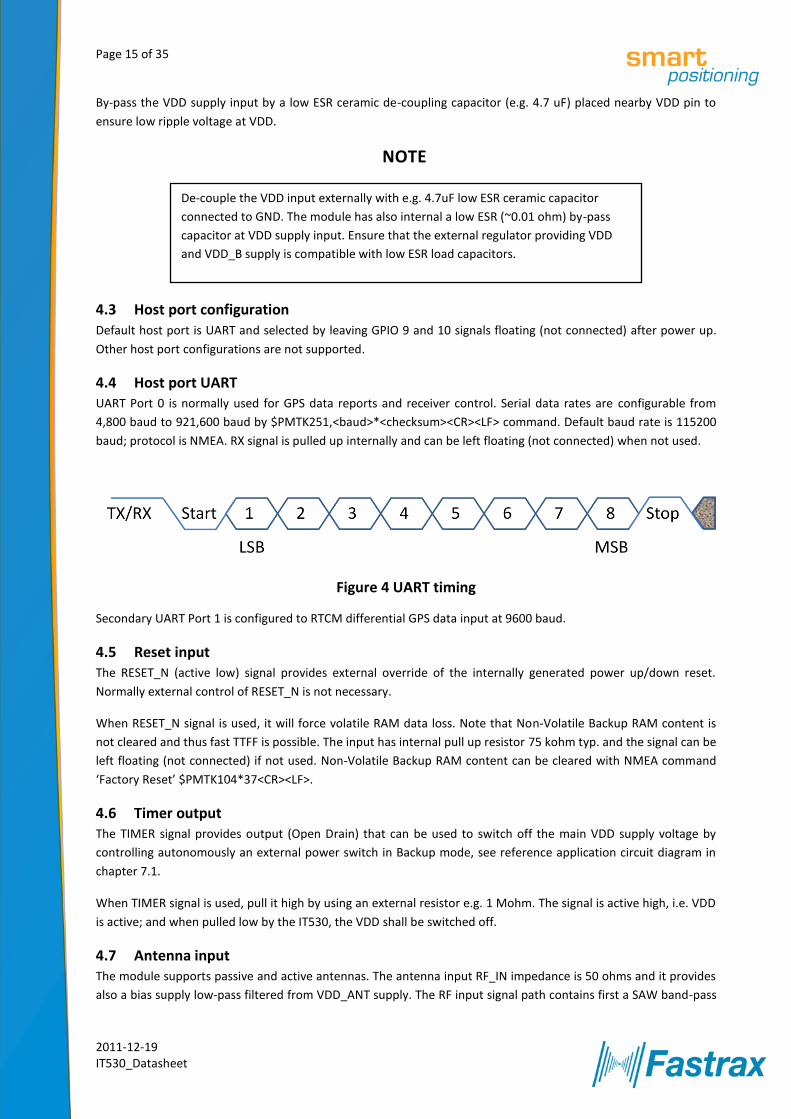
4.4 Host port UART UART Port 0 is normally used for GPS data reports and receiver control. Serial data rates are configurable from
4,800 baud to 921,600 baud by $PMTK251,<baud>*<checksum><CR><LF> command. Default baud rate is 115200
baud; protocol is NMEA. RX signal is pulled up internally and can be left floating (not connected) when not used.
Figure 4 UART timing
Secondary UART Port 1 is configured to RTCM differential GPS data input at 9600 baud.
4.5 Reset input The RESET_N (active low) signal provides external override of the internally generated power up/down reset.
Normally external control of RESET_N is not necessary.
When RESET_N signal is used, it will force volatile RAM data loss. Note that Non-Volatile Backup RAM content is
not cleared and thus fast TTFF is possible. The input has internal pull up resistor 75 kohm typ. and the signal can be
left floating (not connected) if not used. Non-Volatile Backup RAM content can be cleared with NMEA command
‘Factory Reset’ $PMTK104*37<CR><LF>.
4.6 Timer output The TIMER signal provides output (Open Drain) that can be used to switch off the main VDD supply voltage by
controlling autonomously an external power switch in Backup mode, see reference application circuit diagram in
chapter 7.1.
When TIMER signal is used, pull it high by using an external resistor e.g. 1 Mohm. The signal is active high, i.e. VDD
is active; and when pulled low by the IT530, the VDD shall be switched off.
4.7 Antenna input The module supports passive and active antennas. The antenna input RF_IN impedance is 50 ohms and it provides
also a bias supply low-pass filtered from VDD_ANT supply. The RF input signal path contains first a SAW band-pass
De-couple the VDD input externally with e.g. 4.7uF low ESR ceramic capacitor
connected to GND. The module has also internal a low ESR (~0.01 ohm) by-pass
capacitor at VDD supply input. Ensure that the external regulator providing VDD
and VDD_B supply is compatible with low ESR load capacitors.

Page 16 of 35
2011-12-19 IT530_Datasheet
filter before internal LNA, which provides good out-of-band protection against GPS blocking caused by possible
near-by wireless transmitters.
Note that antenna input is ESD sensitive. With passive antennas the ESD performance can be improved by
connecting VDD_ANT supply input to GND. Also an external TVS diode with low capacitance (<0.5pF, e.g. Infineon
ESD0P2RF) can be used to improve RF-input ESD capability.
NOTE
4.8 Active GPS antenna
The customer may use an external active GPS antenna when antenna cable loss exceeds > 1dB. It is suggested the
active antenna has a net gain including cable loss in the range from +10 dB to +25 dB. Specified sensitivity is
measured with external low noise (NF<1dB, G>15dB) amplifier, which gives about 3 dB advantage in sensitivity
when compared to a passive antenna.
An active antenna requires certain bias voltage, which can be supplied externally via VDD_ANT supply input. De-
couple externally the VDD_ANT input; see the application circuit diagram in chapter 6. The external bias supply
must provide limitation of the max current below 150mA during e.g. antenna cable short circuit condition.
When the module is in Standby/Backup mode, the antenna bias can be switched off externally by using WAKEUP
signal output to switch off VDD_ANT supply, see e.g. Application Circuit Diagram.
NOTE
4.8.1 Jamming Remover Jamming Remover is an embedded HW block called AIC (Active Interference Cancellation) that tracks and removes
up to 12 pcs CW (Carrier Wave) type signals up to -80 dBm (total power signal levels). By default the AIC is disabled
and usage requires an NMEA command $PMTK286,1*23<CR><LF> to enable.
Jamming Remover can be used for solving EMI problems in the customer’s system and it is effective against e.g.
narrow band clock harmonics. When enabled, Jammer Remover will increase current drain by about 1 mA and
impact on GPS performance is low at modest jamming levels; however at high jammer levels -90… -80 dBm the RF
signal sampling (ADC) starts to get saturated after which GPS signal levels start to reduce.
Note that Jamming Remover is not effective against wide band noise (e.g. from host CPU memory bus), which
cannot be separated from thermal noise floor. Wide band Jamming signal increases effective noise floor and
eventually reduces GPS signal levels.
With an Active GPS Antenna provide antenna supply externally via VDD_ANT. The
VDD_ANT supply must provide also short circuit protection externally, rated
current 70mA, abs. max. 150mA.
With Passive antennas leave VDD_ANT not connected or connect to GND.
Page 17 of 35
2011-12-19 IT530_Datasheet
4.9 PPS output The PPS output signal provides pulse-per-second output pulse signal for timing purposes. Pulse length (high state)
is 100 ms and it has 1us accuracy synchronized at rising edge to full UTC second with nominal GPS signal levels.
The PPS will output PPS after a few seconds from first fix after the fix epoch is synchronized to full second.
The PPS output is valid when navigation is valid and will also continue ‘freewheel’ after valid fix is lost by a certain
navigation DR timeout, typ. 10 seconds. User can also enable NMEA $GPZDA message that is sent right after the
PPS pulse just sent.
4.10 Wakeup output The WAKEUP output voltage provides indication to e.g. external LNA bias switch that the module is active and
navigation. Polarity is active high = LNA bias active.
WAKEUP output is intended to drive only CMOS inputs; do not load WAKEUP signal with current exceeding 2mA.
Only loads with steady state current drain is allowed (i.e. loads with ripple currents are prohibited).
NOTE
4.11 Interrupt input EINT1 The default EINT1 function is Standby mode control but the function is not supported; leave signal floating (not
connected).
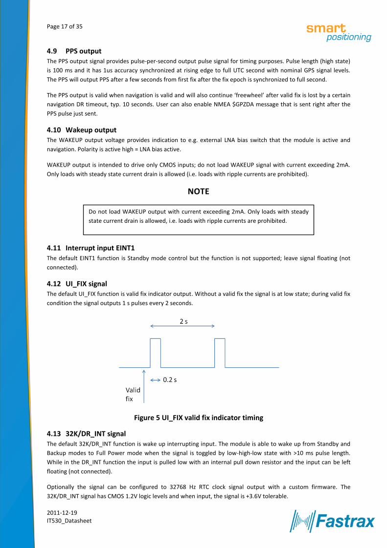
4.12 UI_FIX signal The default UI_FIX function is valid fix indicator output. Without a valid fix the signal is at low state; during valid fix
condition the signal outputs 1 s pulses every 2 seconds.
Figure 5 UI_FIX valid fix indicator timing
4.13 32K/DR_INT signal The default 32K/DR_INT function is wake up interrupting input. The module is able to wake up from Standby and
Backup modes to Full Power mode when the signal is toggled by low-high-low state with >10 ms pulse length.
While in the DR_INT function the input is pulled low with an internal pull down resistor and the input can be left
floating (not connected).
Optionally the signal can be configured to 32768 Hz RTC clock signal output with a custom firmware. The
32K/DR_INT signal has CMOS 1.2V logic levels and when input, the signal is +3.6V tolerable.
Do not load WAKEUP output with current exceeding 2mA. Only loads with steady
state current drain is allowed, i.e. loads with ripple currents are prohibited.
Page 18 of 35
2011-12-19 IT530_Datasheet
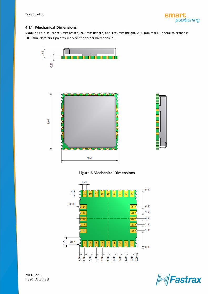
4.14 Mechanical Dimensions Module size is square 9.6 mm (width), 9.6 mm (length) and 1.95 mm (height, 2.25 mm max). General tolerance is
0.3 mm. Note pin 1 polarity mark on the corner on the shield.
Figure 6 Mechanical Dimensions
Page 19 of 35
2011-12-19 IT530_Datasheet
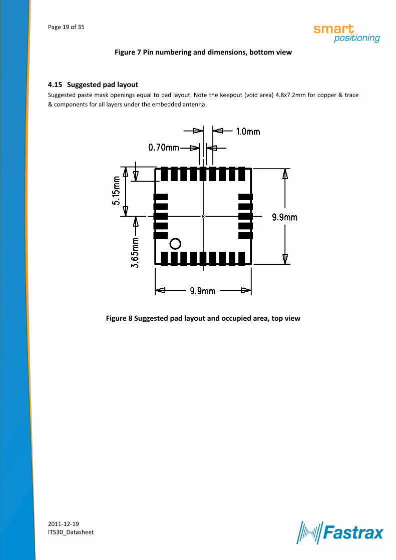
Figure 7 Pin numbering and dimensions, bottom view
4.15 Suggested pad layout Suggested paste mask openings equal to pad layout. Note the keepout (void area) 4.8x7.2mm for copper & trace
& components for all layers under the embedded antenna.
Figure 8 Suggested pad layout and occupied area, top view
Page 20 of 35
2011-12-19 IT530_Datasheet
5 Electrical Specifications
5.1 Absolute Maximum Ratings Stressing the device beyond the Absolute Maximum Ratings may cause permanent damage. Operation beyond the
DC Electrical Specifications is not recommended and extended exposure beyond the Recommended Operating
Conditions can affect device reliability.
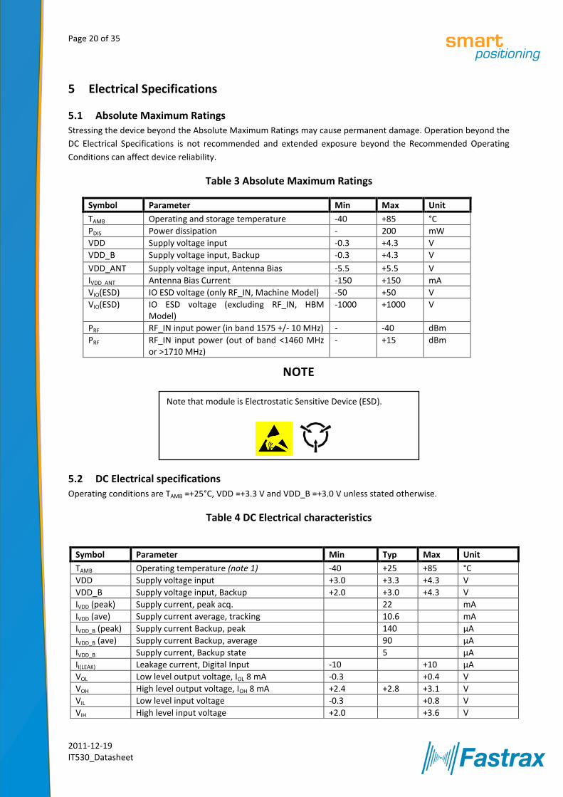
Table 3 Absolute Maximum Ratings
Symbol Parameter Min Max Unit
TAMB Operating and storage temperature -40 +85 °C
PDIS Power dissipation - 200 mW
VDD Supply voltage input -0.3 +4.3 V
VDD_B Supply voltage input, Backup -0.3 +4.3 V
VDD_ANT Supply voltage input, Antenna Bias -5.5 +5.5 V
IVDD_ANT Antenna Bias Current -150 +150 mA
VIO(ESD) IO ESD voltage (only RF_IN, Machine Model) -50 +50 V
VIO(ESD) IO ESD voltage (excluding RF_IN, HBM Model)
-1000 +1000 V
PRF RF_IN input power (in band 1575 +/- 10 MHz) - -40 dBm
PRF RF_IN input power (out of band <1460 MHz or >1710 MHz)
- +15 dBm
NOTE
5.2 DC Electrical specifications
Operating conditions are TAMB =+25°C, VDD =+3.3 V and VDD_B =+3.0 V unless stated otherwise.
Table 4 DC Electrical characteristics
Symbol Parameter Min Typ Max Unit
TAMB Operating temperature (note 1) -40 +25 +85 °C
VDD Supply voltage input +3.0 +3.3 +4.3 V
VDD_B Supply voltage input, Backup +2.0 +3.0 +4.3 V
IVDD (peak) Supply current, peak acq. 22 mA
IVDD (ave) Supply current average, tracking 10.6 mA
IVDD_B (peak) Supply current Backup, peak 140 µA
IVDD_B (ave) Supply current Backup, average 90 µA
IVDD_B Supply current, Backup state 5 µA
II(LEAK) Leakage current, Digital Input -10 +10 µA
VOL Low level output voltage, IOL 8 mA -0.3 +0.4 V
VOH High level output voltage, IOH 8 mA +2.4 +2.8 +3.1 V
VIL Low level input voltage -0.3 +0.8 V
VIH High level input voltage +2.0 +3.6 V
Note that module is Electrostatic Sensitive Device (ESD).

Page 21 of 35
2011-12-19 IT530_Datasheet
Note 1: Operation in the temperature range –40°C… –30°C is allowed but Time-to-First-Fix performance
and tracking sensitivity may be degraded.
Table 5 DC Electrical characteristics, 1.2 V CMOS domain (TIMER & 32K/DR_INT)
5.3 AC Electrical characteristics Operating conditions are TAMB =+25°C and VDD =+1.8 V unless stated otherwise.
Table 6 AC Electrical characteristics
Note 1: with nominal GPS signal levels -130dBm.
Note 2: when enabled by I/O configuration.
RPU Internal Pull Up resistor 40 75 190 kohm
RPD Internal Pull Down resistor 40 75 190 kohm
Symbol Parameter Min Typ Max Unit
VOL Low level output voltage, IOL 0.9 mA +0.42 V
VOH High level output voltage, IOH 0.9 mA +0.78 V
VIL Low level input voltage -0.3 +0.54 V
VIH High level input voltage +0.66 +3.6 V
RPU Internal Pull Up resistor 130 560 kohm
RPD Internal Pull Down resistor 130 560 kohm
Symbol Parameter Min Typ Max Unit
tPPS PPS cycle time 1 s
tPPS,H PPS, high state pulse length 100 ms
∆tPPS PPS accuracy, rising edge (note 1) -1 +1 µs
fRTC RTC output (32K/DR_INT) frequency (note 2) 32768 Hz
Page 22 of 35
2011-12-19 IT530_Datasheet
6 Manufacturing
6.1 Assembly and Soldering The IT530 module is intended for SMT assembly and soldering in a Pb-free reflow process on the top side of the
PCB. Suggested solder paste stencil height is 150um minimum to ensure sufficient solder volume. If required paste
mask pad openings can be increased to ensure proper soldering and solder wetting over pads.
Use pre-heating at 150… 180°C for 60… 120 sec. Suggested peak reflow temperature is 235… 245°C (for
SnAg3.0Cu0.5 alloy). Absolute max reflow temperature is 260°C. For details see Fastrax document ‘Soldering
Profile’ ref (7).
Note that module is Electrostatic Sensitive Device (ESD).
NOTE
Avoid also ultrasonic exposure due to internal crystal and SAW components.
The IT530 module meets the requirements of Directive 2002/95/EC of the European Parliament and of the Council
on the Restriction of Hazardous Substance (RoHS). For details contact Fastrax support.
6.2 Moisture sensitivity IT530 module is moisture sensitive at MSL 3 (see the standard IPC/JEDEC J-STD-020C). The module must be stored
in the original moisture barrier bag or if the bag is opened, the module must be repacked or stored in a dry cabin
(according to the standard IPC/JEDEC J-STD-033B). Factory floor life in humid conditions is 1 week for MSL 3.
Moisture barrier bag self life is 1 year; thus it is suggested to assemble modules prior self life expiration. If the
moisture barrier bad self life is exceeded, the modules must be baked prior usage; contact Fastrax support for
details.
6.3 Marking Module marking includes type code, batch code and serial number.
Type code is e.g. IT530rbbbb (may vary), where
IT530 is module type code for IT530
r is incremental firmware revision (e.g. A, may vary)
bbbb is BOM (Bill-of-Materials) revision code (e.g. 4207, may vary)
Batch code is e.g.120208 (may vary), where
1 is factory code
2 is last digit of the year (e.g. 2012)
02 is month (e.g. February)
Note that module is Electrostatic Sensitive Device (ESD).
Page 23 of 35
2011-12-19 IT530_Datasheet
08 is incremental number of the production batch during the month
Serial number is unique for each module having 10 digits including tester code, last two digits of the year, Julian
date code and incremental number.
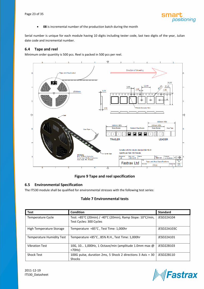
6.4 Tape and reel Minimum order quantity is 500 pcs. Reel is packed in 500 pcs per reel.
Figure 9 Tape and reel specification
6.5 Environmental Specification The IT530 module shall be qualified for environmental stresses with the following test series:
Table 7 Environmental tests
Test Condition Standard
Temperature Cycle
Test: +85°C (20min) / -40°C (20min), Ramp Slope: 10°C/min, Test Cycles: 300 Cycles
JESD22A104
High Temperature Storage
Temperature +85°C , Test Time: 1,000hr JESD22A103C
Temperature Humidity Test
Temperature +85°C , 85% R.H., Test Time: 1,000hr JESD22A101
Vibration Test
10G, 10… 1,000Hz, 1 Octave/min (amplitude 1.0mm max @ <70Hz)
JESD22B103
Shock Test
100G pulse, duration 2ms, 5 Shock 2 directions 3 Axis = 30 Shocks
JESD22B110

Page 24 of 35
2011-12-19 IT530_Datasheet
7 Reference design The idea of the reference design is to give a guideline for the applications using the OEM GPS module. In itself it is
not a finished product, but an example that performs correctly.
In the following two chapters the reader is exposed to design rules that he should follow, when designing the GPS
receiver in to the application. By following the rules one end up having an optimal design with no unexpected
behavior caused by the PCB layout itself. In fact these guidelines are quite general in nature, and can be utilized in
any PCB design related to RF techniques or to high speed logic.
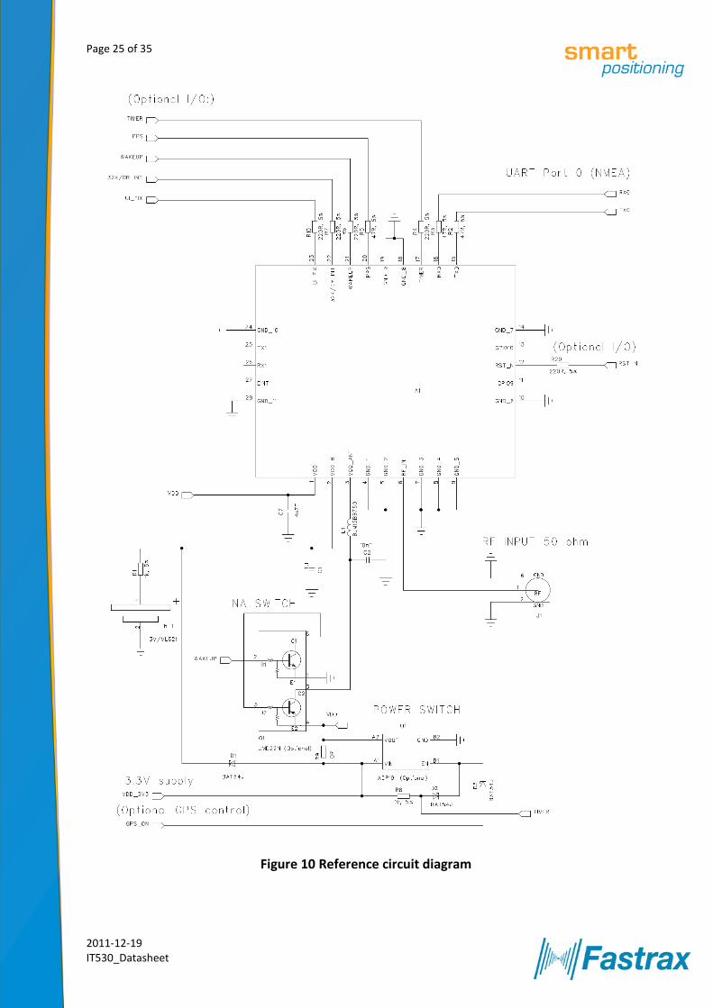
7.1 Reference circuit diagram The following picture describes a minimum connectivity for a typical autonomous navigation application. It
consists of the IT530 module, which is powered by the main VDD supply (+3.3 V typ.) and backup supply VDD_B
(+3.0V typ). The external by-pass capacitor C7 is used to de-couple the VDD supply pin close to pin 1.
Suggestion is to keep the backup supply VDD_B active all the time and host may use the VDD supply to control
module activity between Full Power and Backup operation modes.
The host port is configured to UART by keeping GPIO 9 & 10 floating. Serial port TX output is connected to host
UART input. RX input connection to host UART output is required when sending commands to IT530.
Optionally WAKEUP signal can be used to drive external antenna bias VDD_ANT (+3.3 V typ.) voltage switch (Q1)
during Full Power/Standby/Backup Modes. L1 and C2 provide additional RF decoupling at VDD_ANT supply.
For optional Backup/Periodic modes of operation the external power switch U1 shall be assembled while omitting
by-pass resistor R9 (0R). The U1 power switch shall be controlled autonomously by the TIMER signal from IT530.
Host can over-ride the power switch by GPS_ON control signal via diode D3. The host shall enable GPS operation
after power up by control of GPS_ON signal to high state. After the IT530 has been controlled to Autonomous
Backup Mode or to Periodic Mode via an NMEA message, the module can control VDD activity autonomously via
TIMER signal that has control on the VDD power switch U1.
Optional connectivity to host includes PPS, UI_FIX, 32K/DR_INT signals. UART Port 1 RX1 signal can be used
optionally as input for RTCM differential GPS messages.
Note that all I/O signal levels are CMOS 2.8V compatible (excluding TIMER and 32K/DR_INT signals that have 1.2 V
CMOS domain) and inputs are 3.6 V tolerable.
Some I/O signals have series resistors 47… 220 ohm, which are intended for RF-decoupling purposes to improve
rejection to internally generated EMI that may leak to nearby GPS antenna. If GPS antenna is away > 20cm from
module and/or I/O signals are routed under ground plane these series resistor may be omitted.
Page 25 of 35
2011-12-19 IT530_Datasheet
Figure 10 Reference circuit diagram
Page 26 of 35
2011-12-19 IT530_Datasheet
7.2 PCB layout suggestion
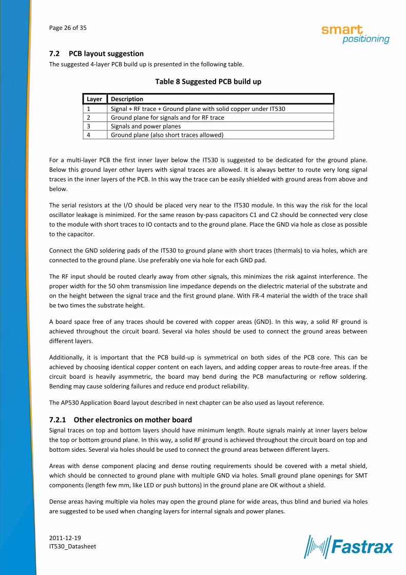
The suggested 4-layer PCB build up is presented in the following table.
Table 8 Suggested PCB build up
Layer Description
1 Signal + RF trace + Ground plane with solid copper under IT530
2 Ground plane for signals and for RF trace
3 Signals and power planes
4 Ground plane (also short traces allowed)
For a multi-layer PCB the first inner layer below the IT530 is suggested to be dedicated for the ground plane.
Below this ground layer other layers with signal traces are allowed. It is always better to route very long signal
traces in the inner layers of the PCB. In this way the trace can be easily shielded with ground areas from above and
below.
The serial resistors at the I/O should be placed very near to the IT530 module. In this way the risk for the local
oscillator leakage is minimized. For the same reason by-pass capacitors C1 and C2 should be connected very close
to the module with short traces to IO contacts and to the ground plane. Place the GND via hole as close as possible
to the capacitor.
Connect the GND soldering pads of the IT530 to ground plane with short traces (thermals) to via holes, which are
connected to the ground plane. Use preferably one via hole for each GND pad.
The RF input should be routed clearly away from other signals, this minimizes the risk against interference. The
proper width for the 50 ohm transmission line impedance depends on the dielectric material of the substrate and
on the height between the signal trace and the first ground plane. With FR-4 material the width of the trace shall
be two times the substrate height.
A board space free of any traces should be covered with copper areas (GND). In this way, a solid RF ground is
achieved throughout the circuit board. Several via holes should be used to connect the ground areas between
different layers.
Additionally, it is important that the PCB build-up is symmetrical on both sides of the PCB core. This can be
achieved by choosing identical copper content on each layers, and adding copper areas to route-free areas. If the
circuit board is heavily asymmetric, the board may bend during the PCB manufacturing or reflow soldering.
Bending may cause soldering failures and reduce end product reliability.
The AP530 Application Board layout described in next chapter can be also used as layout reference.
7.2.1 Other electronics on mother board Signal traces on top and bottom layers should have minimum length. Route signals mainly at inner layers below
the top or bottom ground plane. In this way, a solid RF ground is achieved throughout the circuit board on top and
bottom sides. Several via holes should be used to connect the ground areas between different layers.
Areas with dense component placing and dense routing requirements should be covered with a metal shield,
which should be connected to ground plane with multiple GND via holes. Small ground plane openings for SMT
components (length few mm, like LED or push buttons) in the ground plane are OK without a shield.
Dense areas having multiple via holes may open the ground plane for wide areas, thus blind and buried via holes
are suggested to be used when changing layers for internal signals and power planes.
Page 27 of 35
2011-12-19 IT530_Datasheet
Use a power plane layer dedicated solely for power nets. Use wide trace width or even copper plane areas to
achieve low impedance for power nets. Dedicate at least one layer as ground planes on adjacent layer above or
below power plane layer in order to maximize capacitance to ground plane.
7.2.2 Avoiding EMI Any GPS receiver is vulnerable to external spurious EMI signals since GPS signals are very weak below thermal
noise floor. Any man made noise or spurious signals picked up by the nearby GPS antenna increases the noise floor
and reduces GPS signal levels. Carrier Wave (CW) type spurious signals like clock harmonics on GPS band may also
cause cross correlation products that may interfere with GPS signal tracking and cause position offsets.
The embedded GPS antenna may pick up local EMI signals and thus it is essential for good GPS performance that
the following measures against EMI are properly implemented:
High speed electronics like host CPU & memory bus are enclosed in a ‘Faraday shield’. The electrical enclosure is formed by the ground planes on PCB + metal shield over components. Route signals at inner layers as discussed previously. Use preferably a power plane(s) layer for supply nets.
Any signal that is routed outside the Faraday shield is protected against EMI noise on 1575MHz with a serial RF filter like
o a serial resistor (> 330ohm, suitable for I/O with low current) or o with a dedicated EMI filter (or ferrite bead) suitable for higher current or o with suitable by-pass capacitor e.g. 18pF (low impedance due to series resonance at 1575MHz).
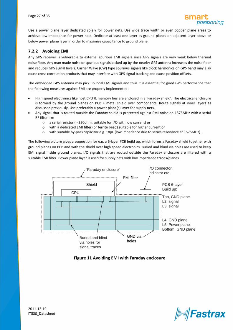
The following picture gives a suggestion for e.g. a 6-layer PCB build up, which forms a Faraday shield together with
ground planes on PCB and with the shield over high speed electronics. Buried and blind via holes are used to keep
EMI signal inside ground planes. I/O signals that are routed outside the Faraday enclosure are filtered with a
suitable EMI filter. Power plane layer is used for supply nets with low impedance traces/planes.
Figure 11 Avoiding EMI with Faraday enclosure
PCB 6-layer
Build up:
I/O connector,
indicator etc.
GND via
holes
CPU
Shield
Top, GND plane
L2, signal
L3, signal
L4, GND plane
L5, Power plane
Bottom, GND plane
Buried and blind
via holes for
signal traces
’Faraday enclosure’
EMI filter
Page 28 of 35
2011-12-19 IT530_Datasheet
8 AP530 Application board for IT530 The Fastrax Application Board AP530 provides the IT530 connectivity to the Fastrax Evaluation Kit or to other
evaluation purposes. It provides a single PCB board equipped with the IT530 module, MCX antenna connector,
Antenna Bias +3.3 V switch, VDD Power Switch, switch for GPS_ON control and 2x20 pin Card Terminal connector.
Default host port configuration is set to UART by switch S4… S6 ‘ON’ and S7 & S8 ‘OFF’. S3 should be ‘ON’ for first
power up; for successive power up and for low power modes the S3 shall be switched to ‘OFF’.
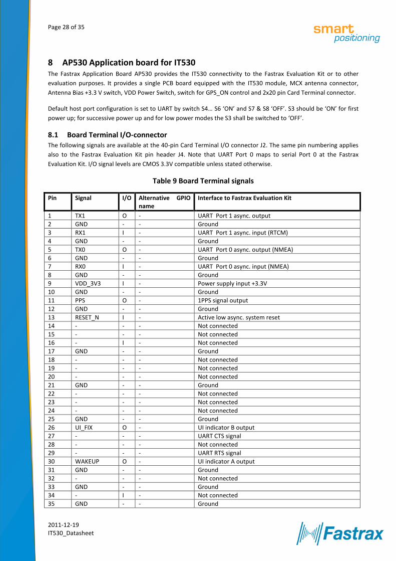
8.1 Board Terminal I/O-connector The following signals are available at the 40-pin Card Terminal I/O connector J2. The same pin numbering applies
also to the Fastrax Evaluation Kit pin header J4. Note that UART Port 0 maps to serial Port 0 at the Fastrax
Evaluation Kit. I/O signal levels are CMOS 3.3V compatible unless stated otherwise.
Table 9 Board Terminal signals
Pin Signal I/O Alternative GPIO name
Interface to Fastrax Evaluation Kit
1 TX1 O - UART Port 1 async. output
2 GND - - Ground
3 RX1 I - UART Port 1 async. input (RTCM)
4 GND - - Ground
5 TX0 O - UART Port 0 async. output (NMEA)
6 GND - - Ground
7 RX0 I - UART Port 0 async. input (NMEA)
8 GND - - Ground
9 VDD_3V3 I - Power supply input +3.3V
10 GND - - Ground
11 PPS O - 1PPS signal output
12 GND - - Ground
13 RESET_N I - Active low async. system reset
14 - - - Not connected
15 - - - Not connected
16 - I - Not connected
17 GND - - Ground
18 - - - Not connected
19 - - - Not connected
20 - - - Not connected
21 GND - - Ground
22 - - - Not connected
23 - - - Not connected
24 - - - Not connected
25 GND - - Ground
26 UI_FIX O - UI indicator B output
27 - - - UART CTS signal
28 - - - Not connected
29 - - - UART RTS signal
30 WAKEUP O - UI indicator A output
31 GND - - Ground
32 - - - Not connected
33 GND - - Ground
34 - I - Not connected
35 GND - - Ground
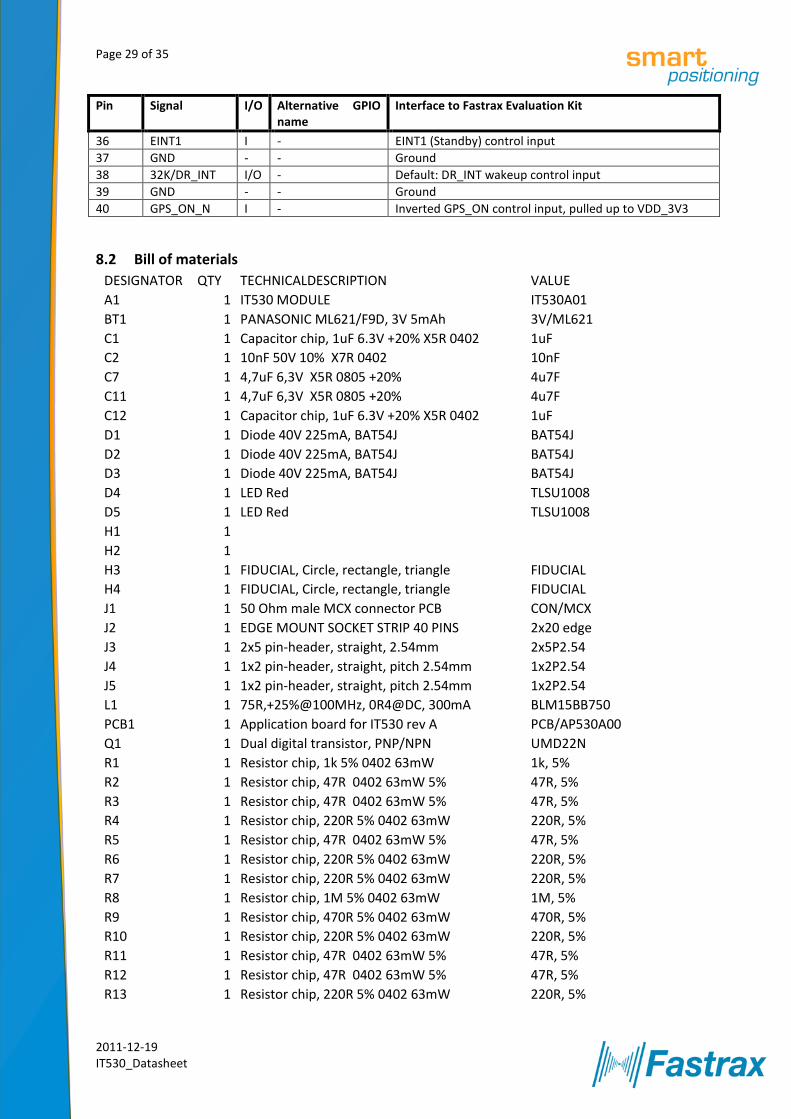
Page 29 of 35
2011-12-19 IT530_Datasheet
Pin Signal I/O Alternative GPIO name
Interface to Fastrax Evaluation Kit
36 EINT1 I - EINT1 (Standby) control input
37 GND - - Ground
38 32K/DR_INT I/O - Default: DR_INT wakeup control input
39 GND - - Ground
40 GPS_ON_N I - Inverted GPS_ON control input, pulled up to VDD_3V3
8.2 Bill of materials
DESIGNATOR QTY TECHNICALDESCRIPTION VALUE
A1 1 IT530 MODULE IT530A01
BT1 1 PANASONIC ML621/F9D, 3V 5mAh 3V/ML621
C1 1 Capacitor chip, 1uF 6.3V +20% X5R 0402 1uF
C2 1 10nF 50V 10% X7R 0402 10nF
C7 1 4,7uF 6,3V X5R 0805 +20% 4u7F
C11 1 4,7uF 6,3V X5R 0805 +20% 4u7F
C12 1 Capacitor chip, 1uF 6.3V +20% X5R 0402 1uF
D1 1 Diode 40V 225mA, BAT54J BAT54J
D2 1 Diode 40V 225mA, BAT54J BAT54J
D3 1 Diode 40V 225mA, BAT54J BAT54J
D4 1 LED Red TLSU1008
D5 1 LED Red TLSU1008
H1 1
H2 1
H3 1 FIDUCIAL, Circle, rectangle, triangle FIDUCIAL
H4 1 FIDUCIAL, Circle, rectangle, triangle FIDUCIAL
J1 1 50 Ohm male MCX connector PCB CON/MCX
J2 1 EDGE MOUNT SOCKET STRIP 40 PINS 2x20 edge
J3 1 2x5 pin-header, straight, 2.54mm 2x5P2.54
J4 1 1x2 pin-header, straight, pitch 2.54mm 1x2P2.54
J5 1 1x2 pin-header, straight, pitch 2.54mm 1x2P2.54
L1 1 75R,+25%@100MHz, 0R4@DC, 300mA BLM15BB750
PCB1 1 Application board for IT530 rev A PCB/AP530A00
Q1 1 Dual digital transistor, PNP/NPN UMD22N
R1 1 Resistor chip, 1k 5% 0402 63mW 1k, 5%
R2 1 Resistor chip, 47R 0402 63mW 5% 47R, 5%
R3 1 Resistor chip, 47R 0402 63mW 5% 47R, 5%
R4 1 Resistor chip, 220R 5% 0402 63mW 220R, 5%
R5 1 Resistor chip, 47R 0402 63mW 5% 47R, 5%
R6 1 Resistor chip, 220R 5% 0402 63mW 220R, 5%
R7 1 Resistor chip, 220R 5% 0402 63mW 220R, 5%
R8 1 Resistor chip, 1M 5% 0402 63mW 1M, 5%
R9 1 Resistor chip, 470R 5% 0402 63mW 470R, 5%
R10 1 Resistor chip, 220R 5% 0402 63mW 220R, 5%
R11 1 Resistor chip, 47R 0402 63mW 5% 47R, 5%
R12 1 Resistor chip, 47R 0402 63mW 5% 47R, 5%
R13 1 Resistor chip, 220R 5% 0402 63mW 220R, 5%
Page 30 of 35
2011-12-19 IT530_Datasheet
R14 1 Resistor chip, 220R 5% 0402 63mW 220R, 5%
R15 1 Resistor chip, 470R 5% 0402 63mW 470R, 5%
R16 1 Resistor chip, 10k 5% 0402 63mW N/A
R17 1 Resistor chip, 10k 5% 0402 63mW 10k, 5%
R20 1 Resistor chip, 220R 5% 0402 63mW 220R, 5%
R21 1 Resistor chip, 220R 5% 0402 63mW 220R, 5%
R26 1 Resistor chip, 10k 5% 0402 63mW 10k, 5%
R27 1 Resistor chip, 10k 5% 0402 63mW 10k, 5%
R33 1 Resistor chip, 10k 5% 0402 63mW N/A
S1 1 Jumper, Pitch, 2.54mm, Red colour J4/P1-P2
S2 1 Label 13x16mm iTrax03s STICKER13x16
S3 1 Switch, on-off SW JMP 2P54
S4 1 Switch, on-off SW JMP 2P54
S5 1 Switch, on-off SW JMP 2P54
S6 1 Switch, on-off SW JMP 2P54
S7 1 Switch, on-off SW JMP 2P54
S8 1 Switch, on-off SW JMP 2P54
S9 1 Jumper, Pitch, 2.54mm, Red colour J5/P1-P2
U1 1 POWER SWITCH 0.1 ohm ADP191
U4 1 Schmit-Trigger inverter NC7SZ14M5X

Page 31 of 35
2011-12-19 IT530_Datasheet
8.3 AP530 Circuit diagram
Figure 12 AP530 Circuit diagram
Page 32 of 35
2011-12-19 IT530_Datasheet
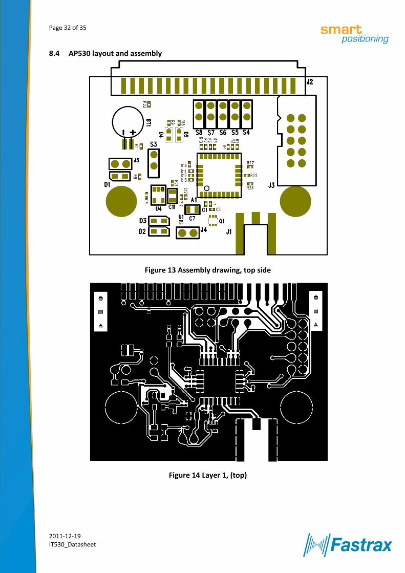
8.4 AP530 layout and assembly
Figure 13 Assembly drawing, top side
Figure 14 Layer 1, (top)

Page 33 of 35
2011-12-19 IT530_Datasheet
Figure 15 Layer 2
Figure 16 Layer 3
Page 34 of 35
2011-12-19 IT530_Datasheet
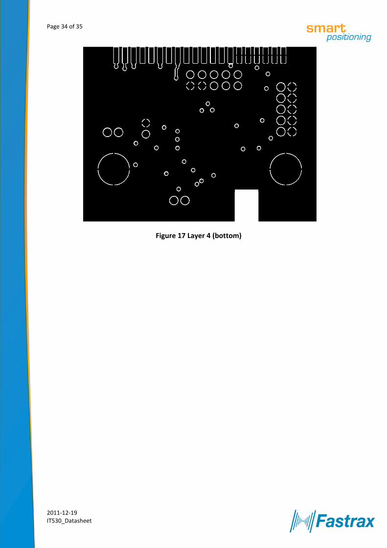
Figure 17 Layer 4 (bottom)

Page 35 of 35
2011-12-19 IT530_Datasheet
Contact Information
Fastrax Ltd
Street Address: Fastrax Ltd
Polaris Business Park
Itsehallintokuja 6
02600 Espoo
Finland
Tel: +358 (0)424 733 1
Fax: +358 (0)9 8240 9691
http://www.fastraxgps.com
E-mail:
Sales: [email protected]
Support: [email protected]