Embed Size (px)
Citation preview
All Rights Reserved, Copyright© FUJITSU LIMITED 2013
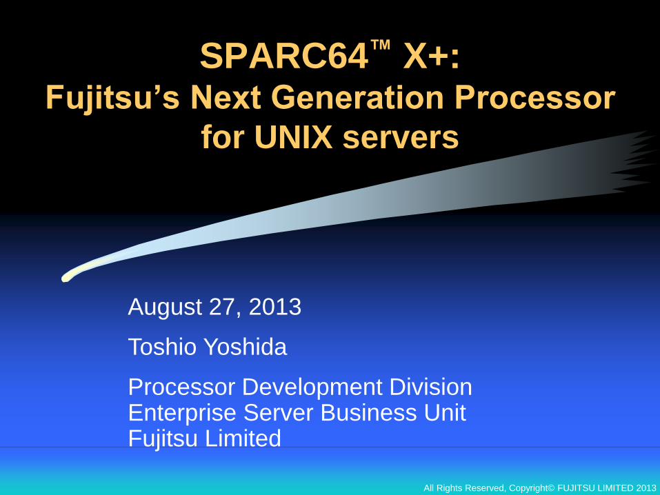
SPARC64™ X+: Fujitsu’s Next Generation Processor
for UNIX servers
August 27, 2013
Toshio Yoshida
Processor Development Division Enterprise Server Business Unit Fujitsu Limited
SPARC64™ X+ All Rights Reserved, Copyright© FUJITSU LIMITED 2013 2
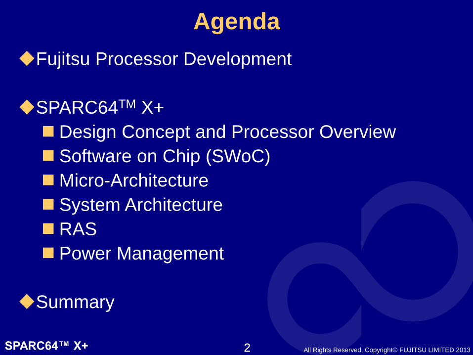
Agenda
Fujitsu Processor Development
SPARC64TM X+
Design Concept and Processor Overview
Software on Chip (SWoC)
Micro-Architecture
System Architecture
RAS
Power Management
Summary
2
SPARC64™ X+ All Rights Reserved, Copyright© FUJITSU LIMITED 2013 3 2000~2003 ~1999
SPARC64
V
SPARC64
GP
GS8900
GS21
600
GS8800B
SPARC64
VII
GS21
SPARC64
V +
SPARC64
VI
GS8800
GS21
900
SPARC64™
Mainframe
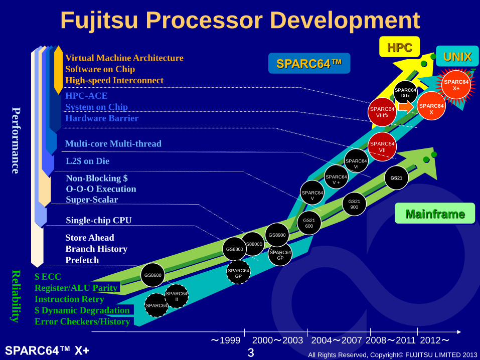
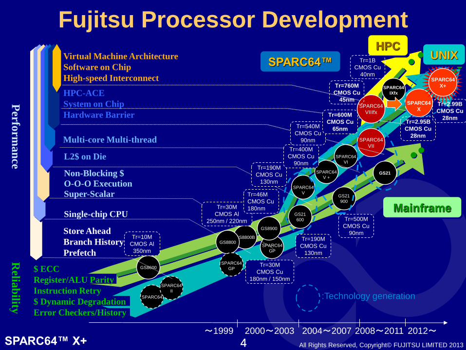
Fujitsu Processor Development
Store Ahead
Branch History
Prefetch
Single-chip CPU
Non-Blocking $
O-O-O Execution
Super-Scalar
L2$ on Die
HPC-ACE
System on Chip
Hardware Barrier
Multi-core Multi-thread
2004~2007 2008~2011
SPARC64
GP
2012~
SPARC64
IXfx
SPARC64
VIIIfx
Virtual Machine Architecture
Software on Chip
High-speed Interconnect
SPARC64
X
SPARC64
X+
SPARC64
SPARC64
II
GS8600
Perfo
rman
ce
Relia
bility
UNIX HPC
$ ECC
Register/ALU Parity
Instruction Retry
$ Dynamic Degradation
Error Checkers/History
3
SPARC64™ X+ All Rights Reserved, Copyright© FUJITSU LIMITED 2013 4 2000~2003 ~1999
SPARC64
SPARC64
II
SPARC64
V
SPARC64
GP
GS8900
GS21
600
GS8600
GS8800B
SPARC64
VII
GS21
SPARC64
V +
SPARC64
VI
GS8800
GS21
900
Mainframe
Perfo
rman
ce
Relia
bility
Fujitsu Processor Development
Store Ahead
Branch History
Prefetch
Single-chip CPU
Non-Blocking $
O-O-O Execution
Super-Scalar
L2$ on Die
HPC-ACE
System on Chip
Hardware Barrier
Multi-core Multi-thread
2004~2007 2008~2011
SPARC64
GP
2012~
SPARC64
IXfx
SPARC64
VIIIfx
Virtual Machine Architecture
Software on Chip
High-speed Interconnect
SPARC64
X
SPARC64
X+
Tr=190M
CMOS Cu
130nm
Tr=30M
CMOS Cu
180nm / 150nm
Tr=190M
CMOS Cu
130nm
Tr=30M
CMOS Al
250nm / 220nm
Tr=46M
CMOS Cu
180nm
:Technology generation
Tr=400M
CMOS Cu
90nm
Tr=500M
CMOS Cu
90nm Tr=10M
CMOS Al
350nm
Tr=760M
CMOS Cu
45nm Tr=2.99B
CMOS Cu
28nm Tr=2.95B
CMOS Cu
28nm
Tr=1B
CMOS Cu
40nm
Tr=540M
CMOS Cu
90nm
Tr=600M
CMOS Cu
65nm
SPARC64™
HPC UNIX
$ ECC
Register/ALU Parity
Instruction Retry
$ Dynamic Degradation
Error Checkers/History
4
SPARC64™ X+ All Rights Reserved, Copyright© FUJITSU LIMITED 2013 5
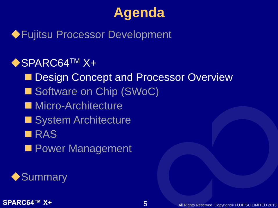
Agenda
Fujitsu Processor Development
SPARC64TM X+
Design Concept and Processor Overview
Software on Chip (SWoC)
Micro-Architecture
System Architecture
RAS
Power Management
Summary
5
SPARC64™ X+ All Rights Reserved, Copyright© FUJITSU LIMITED 2013
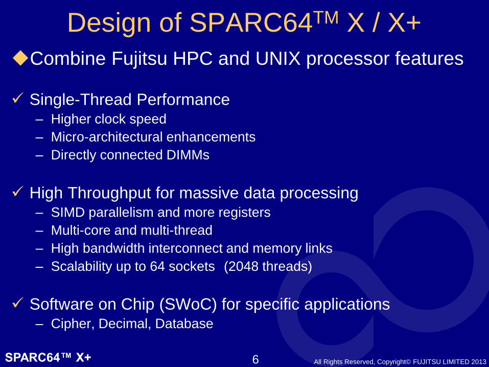
Design of SPARC64TM X / X+
Combine Fujitsu HPC and UNIX processor features
Single-Thread Performance – Higher clock speed
– Micro-architectural enhancements
– Directly connected DIMMs
High Throughput for massive data processing – SIMD parallelism and more registers
– Multi-core and multi-thread
– High bandwidth interconnect and memory links
– Scalability up to 64 sockets (2048 threads)
Software on Chip (SWoC) for specific applications – Cipher, Decimal, Database
6
SPARC64™ X+ All Rights Reserved, Copyright© FUJITSU LIMITED 2013 7
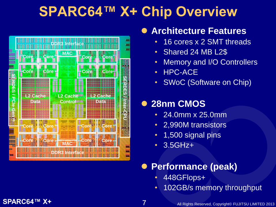
SPARC64™ X+ Chip Overview
Architecture Features • 16 cores x 2 SMT threads
• Shared 24 MB L2$
• Memory and I/O Controllers
• HPC-ACE
• SWoC (Software on Chip)
28nm CMOS • 24.0mm x 25.0mm
• 2,990M transistors
• 1,500 signal pins
• 3.5GHz+
Performance (peak) • 448GFlops+
• 102GB/s memory throughput
DDR3 Interface
DDR3 Interface
Core Core
Core Core
Core Core
Core Core
Core Core
Core Core
Core Core
Core Core
L2 Cache
Data
L2 Cache
Data
L2 Cache
Control
SE
RD
ES
/ Inte
r-CP
U
SE
RD
ES
/ PC
Ie G
en
3
MAC
MAC
7
SPARC64™ X+ All Rights Reserved, Copyright© FUJITSU LIMITED 2013
Control
Registers
PC
FPR 128Registers
GPR 156Registers
8
L1 I$ 64KB
4Way
Branch Target
Address 4Kentry
Decode
& Issue
RSE 24Entry
RSA 24Entry
RSF 20Entry
RSBR 16Entry
GUB 64Registers
GPR 160Registers
EXA
EXB
EAGA
EXC
EAGB
EXD
FPR 128Registers
FUB 64Registers
Fetch
Port 32Entry
Store
Port 24Entry
L1 D$ 64KB
4Way
3port
Memory
Controller
Fetch
(4 stages)
Issue
(4 stages)
Dispatch Reg-Read
(5 stages)
Execute Memory
(L1$: 3 stages)
CSE 96Entry
Commit
(2 stages)
PC
Control
Registers
SPARC64TM X+ Pipeline
L2$ 24MB 24Way
DIMM
Write
Buffer 10Entry
Pattern History Table
32Kentry
IO
Controller
Router
25Gbps x 3ports
14/14.5Gbps x 2ports
PCI-GEN3 CPU-CPU I/F
16-core …
Enhanced in SPARC64TM X+
SWoC
(Cipher,
Decimal,
Database)
FLB
FLC
FLD
FLA
Local Pattern Table
8
SPARC64™ X+ All Rights Reserved, Copyright© FUJITSU LIMITED 2013 9
Agenda
Fujitsu Processor Development
SPARC64TM X+
Design Concept and Processor Overview
Software on Chip (SWoC)
Micro-Architecture
System Architecture
RAS
Power Management
Summary
9
SPARC64™ X+ All Rights Reserved, Copyright© FUJITSU LIMITED 2013
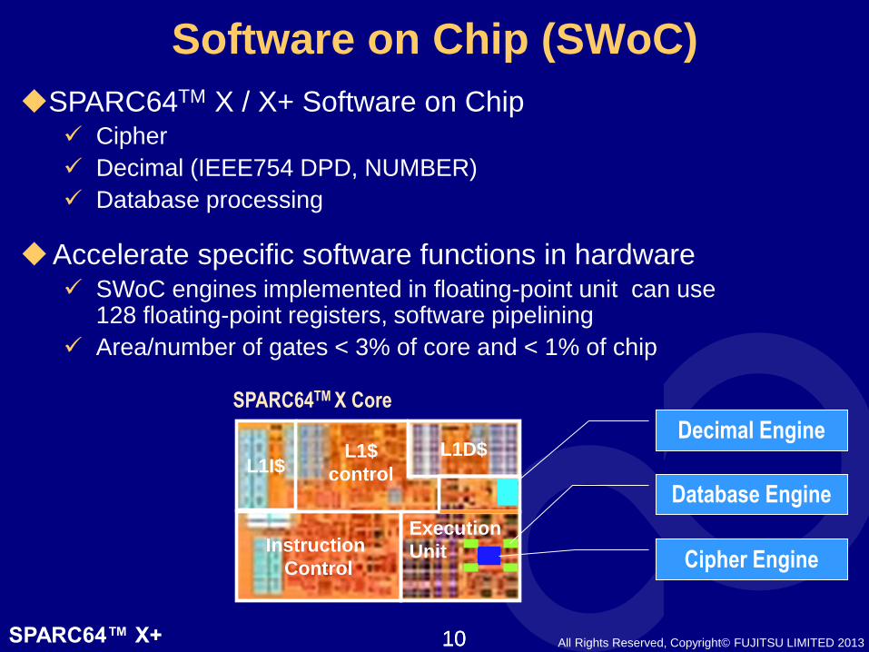
Software on Chip (SWoC)
SPARC64TM X / X+ Software on Chip Cipher
Decimal (IEEE754 DPD, NUMBER)
Database processing
Accelerate specific software functions in hardware SWoC engines implemented in floating-point unit can use
128 floating-point registers, software pipelining
Area/number of gates < 3% of core and < 1% of chip
10
SPARC64TM X Core
L1$
control L1I$ L1D$
Instruction
Control
Execution
Unit
Cipher Engine
Decimal Engine
Database Engine
10
SPARC64™ X+ All Rights Reserved, Copyright© FUJITSU LIMITED 2013
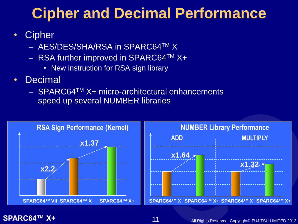
Cipher and Decimal Performance
• Cipher – AES/DES/SHA/RSA in SPARC64TM X
– RSA further improved in SPARC64TM X+
• New instruction for RSA sign library
• Decimal – SPARC64TM X+ micro-architectural enhancements
speed up several NUMBER libraries
SPARC64TM VII SPARC64TM X SPARC64TM X+ SPARC64TM X+
x2.2
x1.37
x1.64
RSA Sign Performance (Kernel)
x1.32
SPARC64TM X+ SPARC64TM X SPARC64TM X
NUMBER Library Performance
ADD MULTIPLY
11
SPARC64™ X+ All Rights Reserved, Copyright© FUJITSU LIMITED 2013
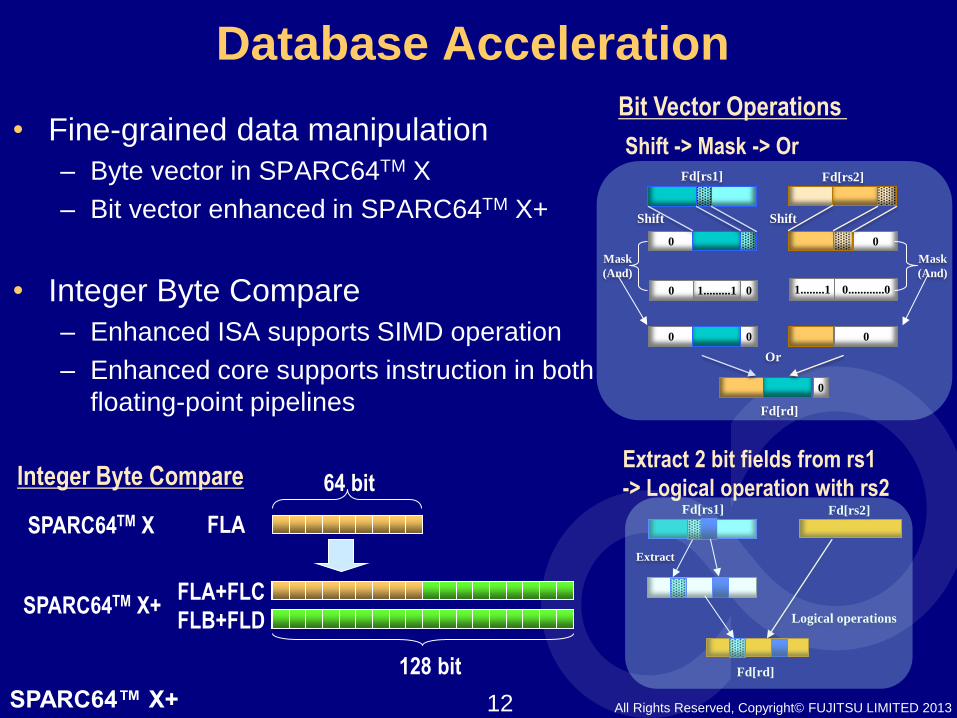
Database Acceleration
• Fine-grained data manipulation
– Byte vector in SPARC64TM X
– Bit vector enhanced in SPARC64TM X+
• Integer Byte Compare
– Enhanced ISA supports SIMD operation
– Enhanced core supports instruction in both
floating-point pipelines
1........1 0............0 1.........1 0 0
0
0
0
0 0
0
Mask
(And)
Mask
(And)
Fd[rs1] Fd[rs2]
Fd[rd]
Fd[rs1] Fd[rs2]
Logical operations
Bit Vector Operations
Extract 2 bit fields from rs1
-> Logical operation with rs2 Integer Byte Compare
SPARC64TM X
SPARC64TM X+
FLA
FLA+FLC
FLB+FLD
Fd[rd]
64 bit
128 bit
Shift -> Mask -> Or
Shift Shift
Or
Extract
12
SPARC64™ X+ All Rights Reserved, Copyright© FUJITSU LIMITED 2013 13
Agenda
Fujitsu Processor Development
SPARC64TM X+
Design Concept and Processor Overview
Software on Chip (SWoC)
Micro-Architecture
System Architecture
RAS
Power Management
Summary
13
SPARC64™ X+ All Rights Reserved, Copyright© FUJITSU LIMITED 2013
Global
Registers
Register
Window
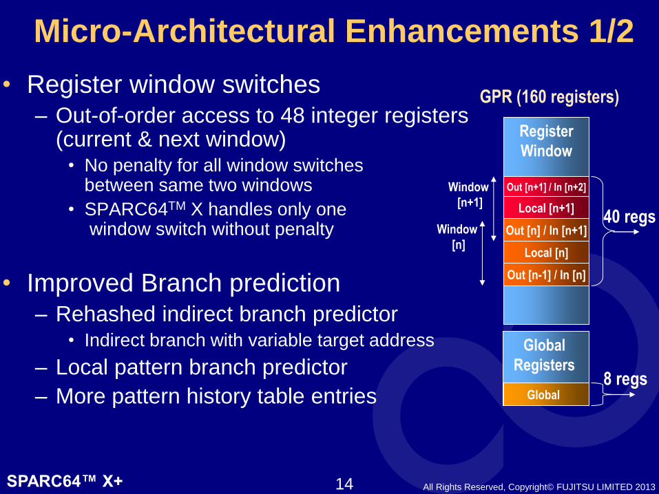
Micro-Architectural Enhancements 1/2
• Register window switches – Out-of-order access to 48 integer registers
(current & next window) • No penalty for all window switches
between same two windows
• SPARC64TM X handles only one window switch without penalty
• Improved Branch prediction – Rehashed indirect branch predictor
• Indirect branch with variable target address
– Local pattern branch predictor
– More pattern history table entries
Out [n] / In [n+1]
Local [n+1]
Out [n+1] / In [n+2]
Out [n-1] / In [n]
Local [n]
Window
[n+1]
Window
[n]
Global
GPR (160 registers)
40 regs
8 regs
14
SPARC64™ X+ All Rights Reserved, Copyright© FUJITSU LIMITED 2013
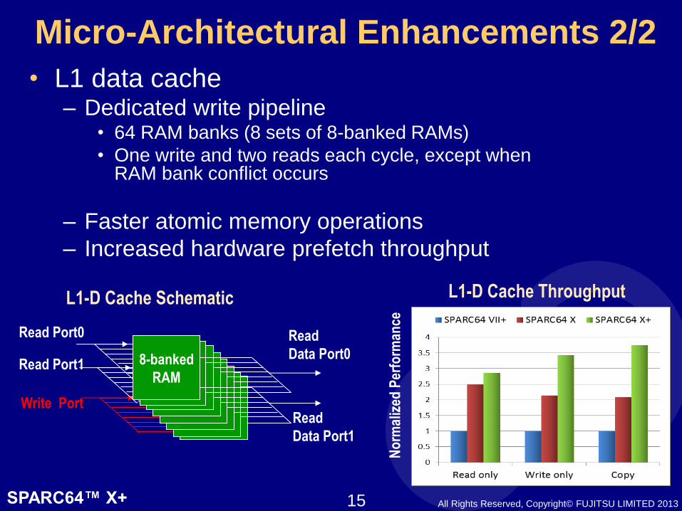
• L1 data cache – Dedicated write pipeline
• 64 RAM banks (8 sets of 8-banked RAMs)
• One write and two reads each cycle, except when RAM bank conflict occurs
– Faster atomic memory operations
– Increased hardware prefetch throughput
L1D$
Read Port0
Read Port1
Write Port
L1-D Cache Schematic
L1D$ L1D$ L1D$ L1D$ L1D$
Read
Data Port0
Read
Data Port1
L1-D Cache Throughput
L1D$ 8-banked
RAM
Micro-Architectural Enhancements 2/2
No
rmal
ized
Per
form
ance
15
SPARC64™ X+ All Rights Reserved, Copyright© FUJITSU LIMITED 2013 16
Agenda
Fujitsu Processor Development
SPARC64TM X+
Design Concept and Processor Overview
Software on Chip (SWoC)
Micro-Architecture
System Architecture
RAS
Power Management
Summary
16
SPARC64™ X+ All Rights Reserved, Copyright© FUJITSU LIMITED 2013
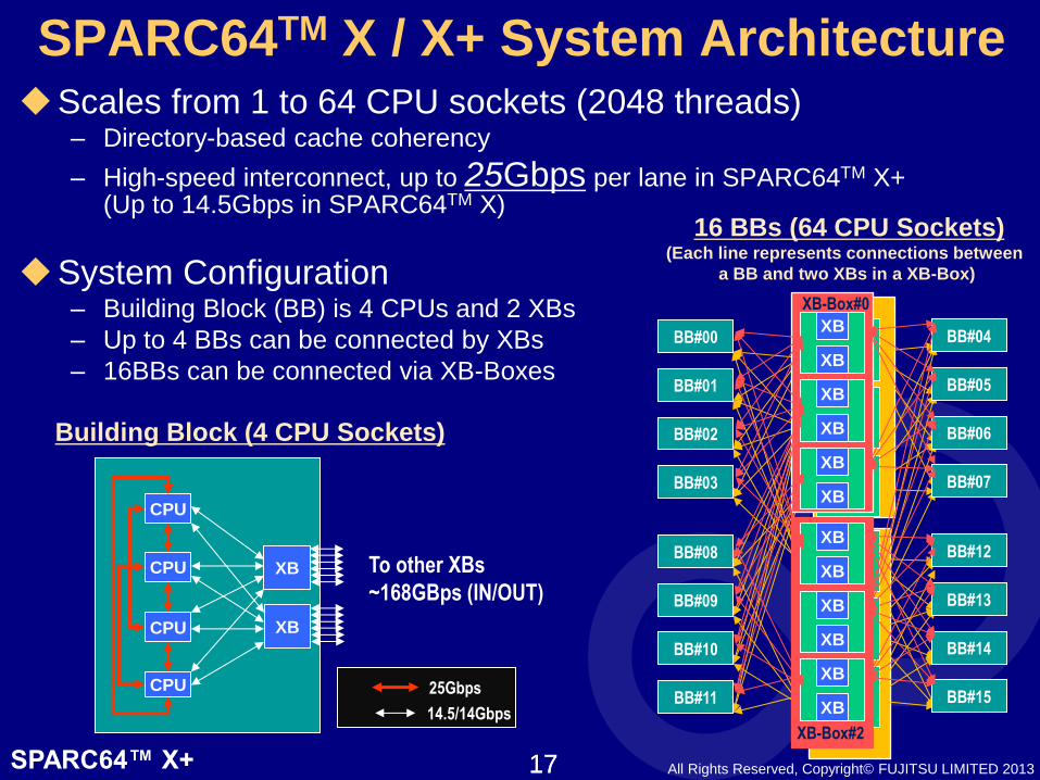
SPARC64TM X / X+ System Architecture Scales from 1 to 64 CPU sockets (2048 threads)
– Directory-based cache coherency
– High-speed interconnect, up to 25Gbps per lane in SPARC64TM X+ (Up to 14.5Gbps in SPARC64TM X)
System Configuration – Building Block (BB) is 4 CPUs and 2 XBs
– Up to 4 BBs can be connected by XBs
– 16BBs can be connected via XB-Boxes
Building Block (4 CPU Sockets)
CPU
CPU
CPU
CPU
XB
XB
25Gbps
14.5/14Gbps
16 BBs (64 CPU Sockets) (Each line represents connections between
a BB and two XBs in a XB-Box)
17
To other XBs
~168GBps (IN/OUT)
BB#00
BB#01
BB#02
BB#03
BB#08
BB#09
BB#10
BB#11
BB#04
BB#05
BB#06
BB#07
BB#12
BB#13
BB#14
BB#15
XB
XB
XB
XB
XB
XB
XB-Box#0
XB-Box#2
XB
XB
XB
XB
XB
XB
17
SPARC64™ X+ All Rights Reserved, Copyright© FUJITSU LIMITED 2013
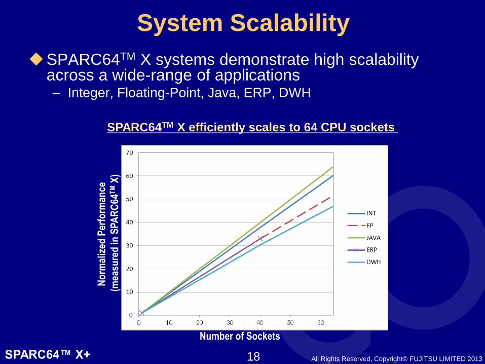
System Scalability
SPARC64TM X systems demonstrate high scalability across a wide-range of applications – Integer, Floating-Point, Java, ERP, DWH
SPARC64TM X efficiently scales to 64 CPU sockets
Number of Sockets
No
rmal
ized
Per
form
ance
(mea
sure
d in
SP
AR
C64
TM
X)
18
SPARC64™ X+ All Rights Reserved, Copyright© FUJITSU LIMITED 2013 19
Agenda
Fujitsu Processor Development
SPARC64TM X+
Design Concept and Processor Overview
Software on Chip (SWoC)
Micro-Architecture
System Architecture
RAS
Power Management
Summary
19
SPARC64™ X+ All Rights Reserved, Copyright© FUJITSU LIMITED 2013
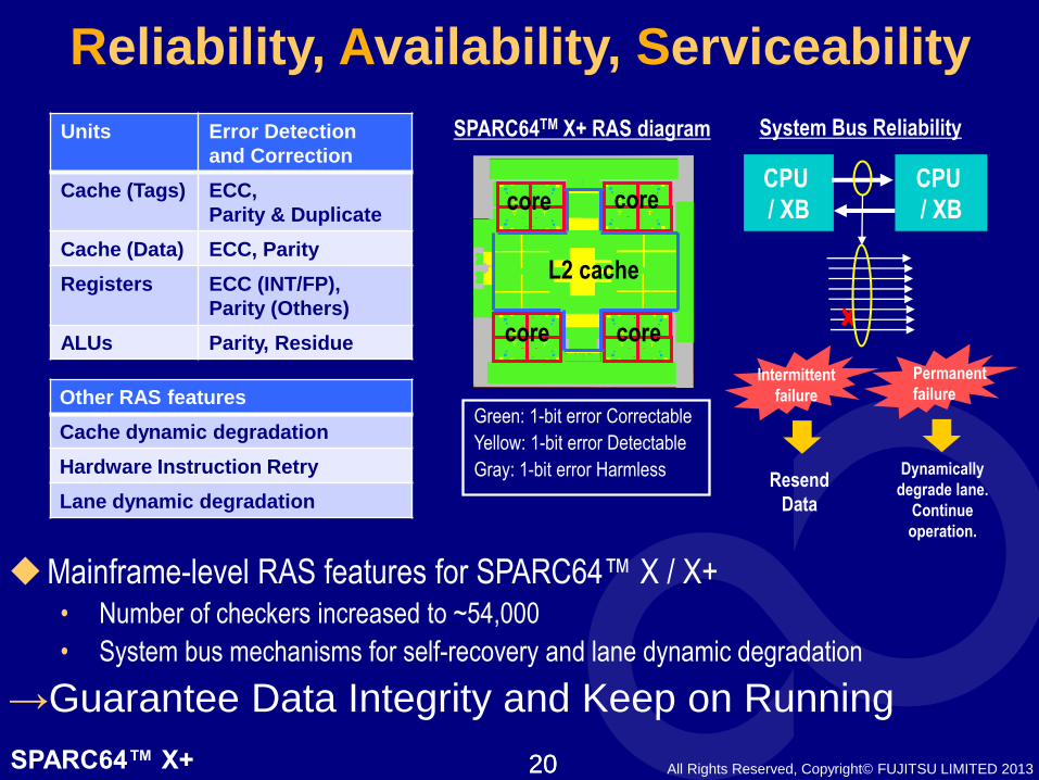
Reliability, Availability, Serviceability
Mainframe-level RAS features for SPARC64™ X / X+ • Number of checkers increased to ~54,000
• System bus mechanisms for self-recovery and lane dynamic degradation
→Guarantee Data Integrity and Keep on Running
Units Error Detection
and Correction
Cache (Tags) ECC,
Parity & Duplicate
Cache (Data) ECC, Parity
Registers ECC (INT/FP),
Parity (Others)
ALUs Parity, Residue
Green: 1-bit error Correctable
Yellow: 1-bit error Detectable
Gray: 1-bit error Harmless
20
SPARC64TM X+ RAS diagram
Other RAS features
Cache dynamic degradation
Hardware Instruction Retry
Lane dynamic degradation
core
core core
core
L2 cache
System Bus Reliability
CPU
/ XB
CPU
/ XB
Intermittent
failure
Resend
Data
Permanent
failure
Dynamically
degrade lane.
Continue
operation.
20
SPARC64™ X+ All Rights Reserved, Copyright© FUJITSU LIMITED 2013 21
Agenda
Fujitsu Processor Development
SPARC64TM X+
Design Concept and Processor Overview
Software on Chip (SWoC)
Micro-Architecture
System Architecture
RAS
Power Management
Summary
21
SPARC64™ X+ All Rights Reserved, Copyright© FUJITSU LIMITED 2013
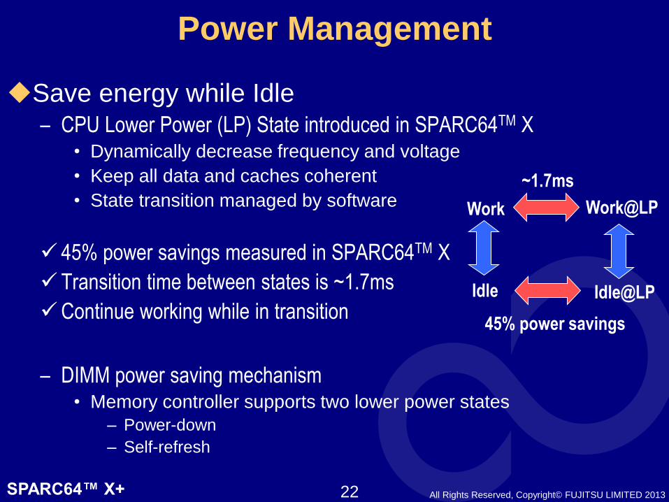
Power Management
Save energy while Idle – CPU Lower Power (LP) State introduced in SPARC64TM X
• Dynamically decrease frequency and voltage
• Keep all data and caches coherent
• State transition managed by software
45% power savings measured in SPARC64TM X
Transition time between states is ~1.7ms
Continue working while in transition
– DIMM power saving mechanism
• Memory controller supports two lower power states
– Power-down
– Self-refresh
Work
Idle
Work@LP
Idle@LP
~1.7ms
45% power savings
22
SPARC64™ X+ All Rights Reserved, Copyright© FUJITSU LIMITED 2013 23
Agenda
Fujitsu Processor Development
SPARC64TM X+
Design Concept and Processor Overview
Software on Chip (SWoC)
Micro-Architecture
System Architecture
RAS
Power Management
Summary
23
SPARC64™ X+ All Rights Reserved, Copyright© FUJITSU LIMITED 2013 24
Summary
SPARC64TM X+ is Fujitsu’s latest SPARC processor, designed for Fujitsu’s next generation UNIX servers
SPARC64TM X+ realizes improved single-thread performance with a higher clock speed, micro-architectural enhancements, and SWoC
SPARC64TM X / X+ systems realize high scalability, from 1 to 64 CPU sockets (2048 threads)
SPARC64TM X+ implements extensive RAS features
Fujitsu will continue to develop the SPARC64TM series
24
SPARC64™ X+ All Rights Reserved, Copyright© FUJITSU LIMITED 2013 25
Abbreviations
• SPARC64TM X+ – RSA: Reservation Station for Address generation
– RSE: Reservation Station for Execution
– RSF: Reservation Station for Floating-point
– RSBR: Reservation Station for Branch
– GUB: General-purpose Update Buffer
– FUB: Floating-point Update Buffer
– GPR: General-Purpose Register
– FPR: Floating-Point Register
– CSE: Commit Stack Entry
– EAG: Effective Address Generator
– EX : Execution unit (Integer)
– FL : Floating-point unit
– HPC-ACE: High Performance Computing-Arithmetic Computational Extensions
– ERP: Enterprise Resource Planning
– DWH: Data WareHouse
25


![[NHN NEXT] 2014 NHN NEXT 창의체험](https://img.pdfslide.tips/doc/110x75/554f3590b4c905cd048b4cf1/nhn-next-2014-nhn-next-.jpg)