Embed Size (px)
Citation preview
SuPER System DC-DC Buck Converter
By
Thaddeus Guno Kunal Shah Koosh Shah
Senior Project
ELECTRICAL ENGINEERING DEPARTMENT
California Polytechnic State University
San Luis Obispo
Spring 2007
ii
Table of Contents
Section Page
Acknowledgements…………………………………………………………..iii
Abstract……………………………………………………………………….iv
List of Tables and Figures……………………………………………………..v
I. Introduction…………………………………………………………………...1
II. Background…………………………………………………………………..3
III. Requirements………………………………………………………………..9
IV. Design……………………………………………………………………...13
V. Construction/Assembly...…………………………………………….……..22
VI. Testing……………………………………………………………..............25
VII. Conclusions and Recommendations……………………………………....34
VIII. Bibliography……………………………………………………………...39
Appendices
A. Parts List, Vendors, Cost …………………………………………………...40
B Simulation Source Code..……………………………………….…………...42
C. Analysis of Senior Project Design...………………………………………..43

iii
Acknowledgements
As a team of three, we would like to give our special thanks to Dr. Harris for
all his support and encouragement throughout our senior project journey. We would
also like to thank all the members of the SuPER team, especially Tyler, for all their
knowledge and assistance. Lastly, we would like to thank our family and friends for
their support through our college career at California Polytechnic State University,
San Luis Obispo.

iv
Abstract
This senior project focuses on the DC-DC converter of the SuPER project.
The DC-DC converter that this senior project focuses on is the Buck Converter, a
simple step down non-isolated DC-DC converter. The DC-DC converter is the heart
of the SuPER project because it provides a physical interface between the solar cell
and the battery and loads. This senior project report will discuss the requirements,
design, and testing of the DC-DC converter. In addition, it will also focus on the
testing and understanding of the high side driver chip used in the DC-DC converter
circuit. Lastly, since the DC-DC Converter was not completed, this report will
include recommendations to the future generation that works on the DC-DC
converter.
v
List of Tables and Figures
Tables Page
Table I: DC-DC Buck Converter Specifications [5]………………………...…...11
Table II: MOSFET Test Results…………………………….……………….…..26
Table III: HSD Testing Data……………………………………………..……....28
Table IV: Data for DC Testing……………………………………………….….30
Table V: Test Results with Inverter and High-side Driver…………………....…33
Table VI: Parts, Vendor, and Cost……………………………………………….40
Figures Page
Figure 1: Simple Buck Converter…………………………………………………3
Figure 2: Simple Buck Converter with SW1 ON…………………………………4
Figure 3: Simple Buck Converter with SW1 OFF…………….……………..........4
Figure 4: Plot Defining Duty Cycle…………………………………………….....5
Figure 5: A Piece of the Simulink Schematic of the Buck Converter…………….8
Figure 6: Transient Response at the Output……………………………………...14
Figure 7: Steady State Output………………………………………………........15
Figure 8: Switching Cycle of MOSFET…………………………………………15
Figure 9: Schematic of the Buck Converter Printed Circuit Board……………...17
Figure 10: First PCB Layout……………………………………………………..20
Figure 11: Second PCB Layout………………………………………………….21
vi
Figure 12: Top View of the High-side Driver Chip……………………………...25
Figure 13: Basic HSD and MOSFET Test……………………………….…........26
Figure 14: HSD Testing Circuit………………………………………….……....28
Figure 15: DC Testing Circuit for HSD………………………………………....30
Figure 16: Circuit Layout of MC14007UB…………………………………...…31
Figure 17: CMOS Inverter Test Circuit………………………………………….31
Figure 18: Input/Output of a Working CMOS Inverter with 5VCC……….…......32
1
I. Introduction
The Sustainable Power for Electric Resources (SuPER) project is originally
proposed by Dr. James Harris. The SuPER project’s main goal is to provide families
in third-world countries a low-cost, sustainable source of electrical power for a span
of 20 years [1]. The project is to design a prototype using today’s technologies while
assuming the possible future technological advancement according to a Moore’s Law
model. The prototype will consist of 4 main subsystems: a solar photovoltaic source,
power control, energy storage (battery), and a standardized DC electrical power
output interface [1].
The SuPER project chose DC, not AC to power the load simply because the
solar photovoltaic source has a DC output and all the basic appliances, like the ones
used in the SuPER project, can be DC based. The many benefits of having a DC load
have mostly to do with power efficiency. Light emitting diodes (LEDs) (today, a 3W
white LED has the same lumens as a standard 60W light bulb), many basic
refrigeration devices, and small electrical motors can be used to pump water for
drinking or irrigation, all could be run by a DC power supply. The SuPER project is
designed as a family unit therefore eliminating DC power transmission line losses.
This report will discuss the DC-DC Buck Converter needed to transfer power
from the solar photovoltaic source to the battery and the rest of the system. The
background section will give information on how a Buck Converter works in theory.
2
The requirements will show the scope of our portion of the project and how it
changed multiple times during the duration of the two quarters. It will also present
the specifications for the Buck Converter. Design will present the simulation design
of the Buck Converter and the PCB layout with the use of PCB123. Construction and
assembly will discuss all the errors we made with the PCB board and the problems
that came up when trying to test the high-side driver. Testing will present our testing
procedures and results. There will also be three appendices at the end: Appendix A
presents a list of all the parts, vendors and prices we used in for the buck; Appendix B
presents the simulation source code for our simulation of the simple Buck Converter;
and Appendix C will present the team’s senior project analysis.
3
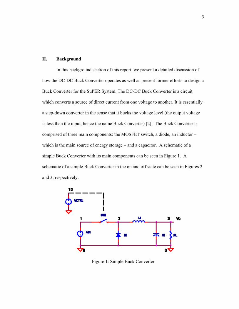
II. Background
In this background section of this report, we present a detailed discussion of
how the DC-DC Buck Converter operates as well as present former efforts to design a
Buck Converter for the SuPER System. The DC-DC Buck Converter is a circuit
which converts a source of direct current from one voltage to another. It is essentially
a step-down converter in the sense that it bucks the voltage level (the output voltage
is less than the input, hence the name Buck Converter) [2]. The Buck Converter is
comprised of three main components: the MOSFET switch, a diode, an inductor –
which is the main source of energy storage – and a capacitor. A schematic of a
simple Buck Converter with its main components can be seen in Figure 1. A
schematic of a simple Buck Converter in the on and off state can be seen in Figures 2
and 3, respectively.
Figure 1: Simple Buck Converter
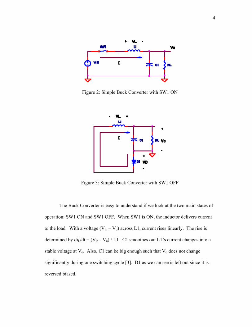
4
Figure 2: Simple Buck Converter with SW1 ON
Figure 3: Simple Buck Converter with SW1 OFF
The Buck Converter is easy to understand if we look at the two main states of
operation: SW1 ON and SW1 OFF. When SW1 is ON, the inductor delivers current
to the load. With a voltage (Vin – Vo) across L1, current rises linearly. The rise is
determined by diL/dt = (Vin - Vo) / L1. C1 smoothes out L1’s current changes into a
stable voltage at Vo. Also, C1 can be big enough such that Vo does not change
significantly during one switching cycle [3]. D1 as we can see is left out since it is
reversed biased.
5
When SW1 is OFF, the inductor maintains current to the load. As L1’s
magnetic field collapses, current falls linearly through L1. The fall is again
determined by the voltage across L1 and its inductance: diL/dt = -Vo / L1. Although
L1’s current direction is the same, the voltage across L1 is negative as seen in Figure
3. This allows L1 to maintain current flow by reversing its voltage when the applied
voltage is removed. Also, D1 turns on when the left end of L1 swings negative,
providing a path for L1’s current to flow [3].
With all the components given, the means to control the output voltage would
be to use a Pulse-Width Modulation (PWM) signal to drive SW1. Since Vo/Vin = D,
where D, duty cycle = Ton/Ts, the desired output voltage can be obtained by
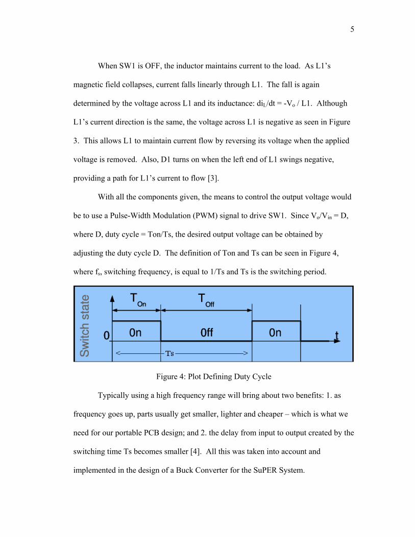
adjusting the duty cycle D. The definition of Ton and Ts can be seen in Figure 4,
where fs, switching frequency, is equal to 1/Ts and Ts is the switching period.
Figure 4: Plot Defining Duty Cycle
Typically using a high frequency range will bring about two benefits: 1. as
frequency goes up, parts usually get smaller, lighter and cheaper – which is what we
need for our portable PCB design; and 2. the delay from input to output created by the
switching time Ts becomes smaller [4]. All this was taken into account and
implemented in the design of a Buck Converter for the SuPER System.

6
The DC-DC Buck Converter is the heart of the whole SuPER system. Two
full years of testing and integration of the buck converter has been done. However,
there has been no success in implementing a successful Buck Converter. The first
Buck Converter used in the SuPER system was the MX60, a high-capacity DC-DC
converter manufactured by Outback Power Systems [5]. Before fall of 2006, two
previous efforts for constructing a functional converter by Eric Phillips and by Robert
Johnson did not succeed. Starting fall of 2006, seniors Robert Casanova and Joe
Shein began new efforts to develop the converter. They worked closely with
Professor Taufik, but ultimately the converter was not successfully integrated with the
SuPER System. The students working on the Buck Converter tried to gain experience
from the past students in order to make their converter work successfully. However,
each group did not succeed in getting a Buck Converter to work with the SuPER
System.
This previous work led to the winter of 2007 development effort by Koosh
Shah, Kunal Shah, and Thaddeus Guno. We tried simulating a design that was
already simulated with the full system design using the Simulink system model. The
simulations we ran with PSpice led to the layout of a high-current PCB. According to
the SuPER System design, there will be a high frequency PWM signal input from a
microcontroller that basically controls the duty cycle of the MOSFET switch on the
Buck Converter. The 500 kHz PWM signal for this converter is sourced by a
microcontroller, and some of the difficulties with this approach involve proper
marriage of this signal to the MOSFET switch [5]. The previous experience led to the
7
realization that a high-side driver chip would be necessary to help turn on the
MOSFET switch in the Buck Converter. Not only that, the high-side driver would
also be needed to keep the MOSFET in the linear region rather than going into the
cut-off or the saturation regions. The implementation and testing of the high-side
driver is what a majority of our testing will focus on.
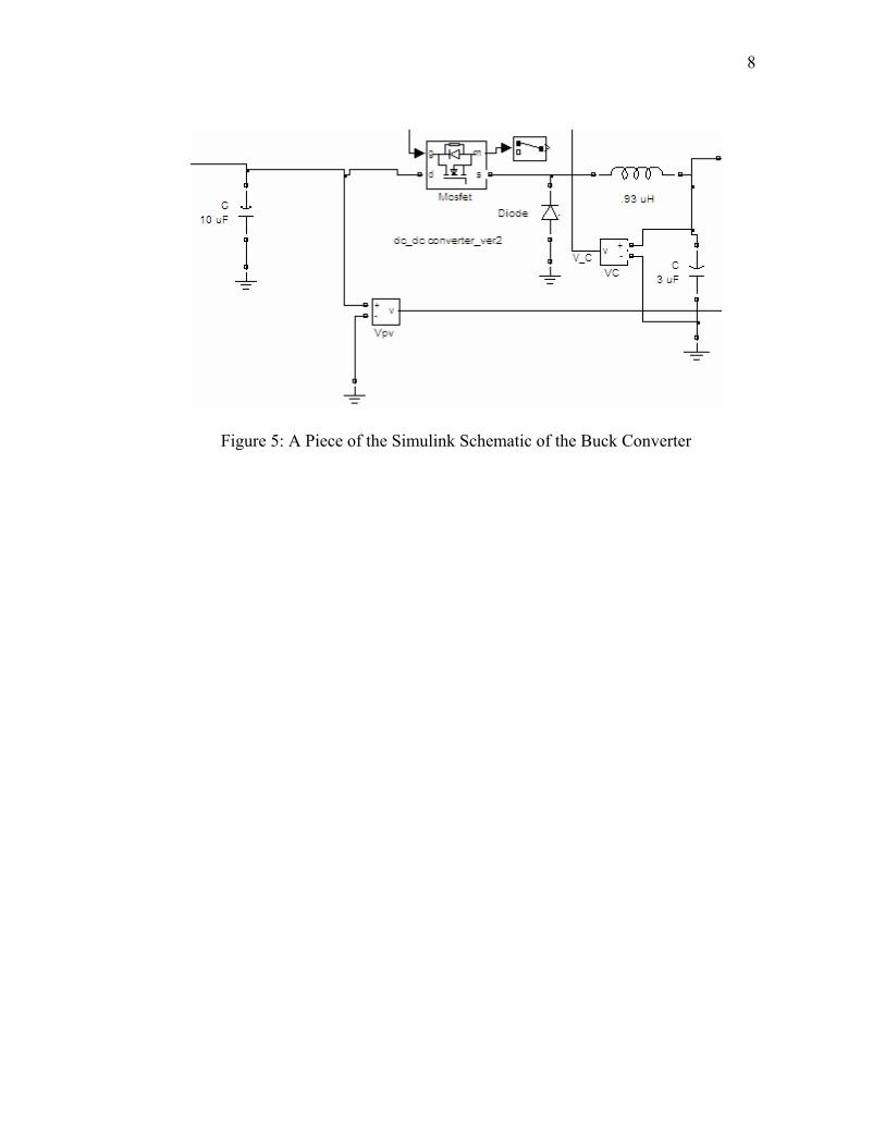
Another problem fixed by Tyler Sheffield has to do with interfacing the
current source to the DC-DC converter in Simulink. As a result of the SuPER
simulation system, it is necessary to include some circuit element in parallel with the
current source. Various options were explored, including resistors and controlled
voltage sources, but a capacitor actually provides the optimum system behavior [5].
An optimal value of the capacitor was found by experimentation to be at about 10uF.
The Simulink model includes this extra capacitor at the input and is something we
took into account when building the layout for our Buck Converter. A part of the
schematic of the Buck Converter taken from the Simulink model with the extra
capacitor included can be seen in Figure 5.
8
Figure 5: A Piece of the Simulink Schematic of the Buck Converter
9
III. Requirements
The requirements for our senior project seemed to change a few times
due to a number of problems encountered during our last quarter of the senior project
journey. Initially, Thaddeus Guno and Koosh Shah were going to build a Cuk
Converter due to its better characteristics and results when compared to the Buck
Converter. After building this converter, preliminary tests would be taken to see if
the converter works. Next, we would integrate the converter with the SuPER System
as a whole. Kunal Shah was going to build up on the past Buck Converter designed
by Robert and Joe. Improvements should be made in order that the past Buck
Converter, which supposedly should handle 150 watts, could be modified and
improved in such a way that it handles up to 400 watts when integrated with the
whole SuPER System.
As more time passed, Robert and John were not able to build a successful
Buck Converter to be worked upon. For this reason, our senior project requirements
changed again in which we were counted on just being able to integrate a Buck
Converter with the SuPER System. The testing that went along with the Buck
Converter and the high-side driver included created more problems. The PCB turned
out to be erroneous and could not be fixed right away. Testing had to be done using a
breadboard with only the high-side driver chip soldered onto the PCB board. Again a
number of problems were encountered with just the high-side driver itself. We could
10
not get the high-side driver to operate properly which once again changed our
requirements as a whole. The whole senior project is clearly a tremendous learning
experience in which we are required to learn everything that we can possibly learn
with the time available. This knowledge can be conveyed to the future generations in
the recommendations section and used wisely to hopefully produce a complete,
integrated Buck Converter. The following section will emphasize in detail the
specifications for the Buck Converter.
Specifications:
The DC-DC Buck Converter provides a physical interface between the solar
cell and the battery and the loads. The converter’s input impedance is the impedance
seen by the PV panel terminals, and is controlled by the converter’s switching duty
cycle [5]. By adjusting the duty cycle and monitoring the converter’s output, a simple
“Perturb and Observe” algorithm for maximum power point tracking can be
implemented [8]. The specifications of the Buck Converter are unchanged since the
start of the SuPER System since a working Buck has yet to be produced.
The Buck Converter needs to be able to handle a wide range of input voltages,
ranging from approximately 24V to 40V, depending on the solar irradiance and the
converter’s own duty cycle. The input current should never exceed more than 4.75A.
The efficiency of the converter should be approximately 80% with a step down in no
more than 150 watts of power. When the battery is charging, the output voltage is
expected to vary from 11.5V to 14V depending on the battery level. In real time, the
converter should be able to output approximately 12V to the battery. Overall, the
11
output voltage ripple should be extremely small – around 50mV. Assuming that the
converter has perfect efficiency, and using the formula for power P = V*I, the
maximum output current should be approximately 13A. Another requirement
specific to building our own Buck Converter on a PCB should make sure all the
terminal blocks or connectors are rated at 30A. The specifications for the Buck
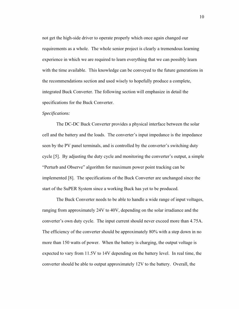
Converter can be seen in tabular form in Table II.
Table I: DC-DC Buck Converter Specifications [5]
The switching frequency used for the current PWM signal is approximately
500 kHz. This rate is defined by the capabilities of the PIC 18F4320 [5]. This
frequency must definitely be taken into account when picking a MOSFET. The
MOSFET should be one that is a high frequency MOSFET which can also handle
high power. As a result we picked a power MOSFET that could be applicable in high
frequency circuits.
For reference, a schematic of the Buck Converter can be seen in Figure 5.
The specifications of all the parts used in our Buck Converter design can be seen in
Appendix A. The energy storage elements (an inductor and capacitor) are key
parameters for the converter and are picked based on the design considerations. The
12
value of the inductor is 0.93mH, and is calculated using the following equation for the
desired maximum output current [5]:
The value of the capacitor at the output is calculated to be 3uF using the equation
which gives the least peak to peak output voltage ripple (ΔVo):
The value of the capacitor at the input was chosen to be 10uF and determined by the
SuPER System simulation. The capacitor is included in our final layout since it also
helps stabilize the change in input voltage.
When picking the type of diode to use, we spoke to Dr. Taufik who mentioned
using a Schottky diode for the Buck. A Schottky diode has very low forward voltage
drop as well as very fast switching action. It is typical to use in a switch-mode power
supply application (Buck Converter). The use of a Schottky diode with low forward
voltage drops also leads to increased efficiency [9].
13
IV. Design
A. Simulation
The first part of the senior project consisted of studying the simulation file of
a simple Buck Converter. The template PSpice .cir file of the Buck Converter was
given to us by Dr. Harris. The .cir file is a template of a Buck Converter in source
code. Since most of our PSpice simulations in our Electrical Engineering courses
were done in schematic form, we had to put in extra effort when working with the
source code. We had to research and find out about the syntax while troubleshooting
with the simulation itself. After some time and study, we came out with the
following simulation results.
Simulation Results:
Our first simulation was initiating the transient analysis at the output. The
source code of our template Buck Converter can be seen in Appendix B. The plot in
Figure 6 shows the output response at the output capacitor with hardly any overshoot
within the initial part of the response. The plot is analyzed with a duty cycle of
approximately 30% in which the output should stabilize to 12V (what we want);
however, according to the plot, the output stabilizes to 11.6V which is extremely
close to the theoretical. The plot as a whole shows how much time it takes to run
from a transient state to a steady state, also known as the settling time. According to
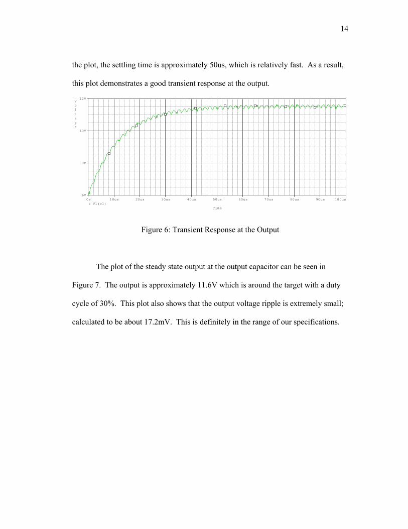
14
the plot, the settling time is approximately 50us, which is relatively fast. As a result,
this plot demonstrates a good transient response at the output.
Time
0s 10us 20us 30us 40us 50us 60us 70us 80us 90us 100usV1(c1)
6V
8V
10V
12VVoltage
Figure 6: Transient Response at the Output
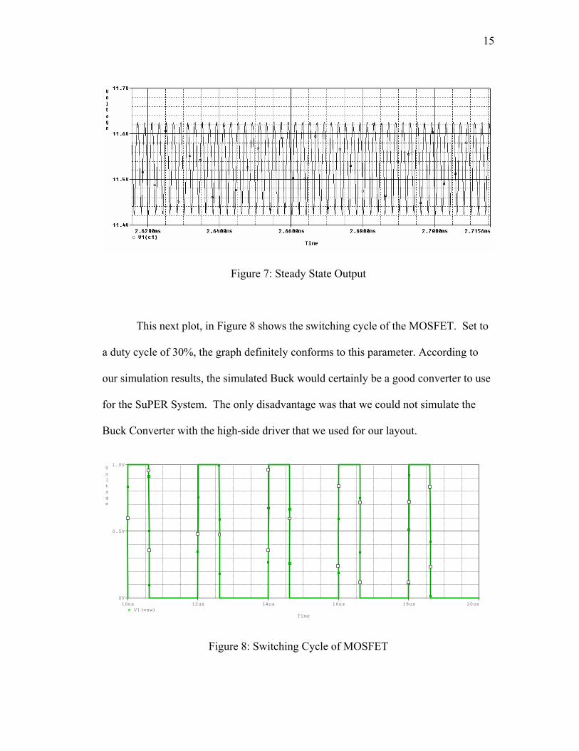
The plot of the steady state output at the output capacitor can be seen in
Figure 7. The output is approximately 11.6V which is around the target with a duty
cycle of 30%. This plot also shows that the output voltage ripple is extremely small;
calculated to be about 17.2mV. This is definitely in the range of our specifications.
15
Figure 7: Steady State Output
This next plot, in Figure 8 shows the switching cycle of the MOSFET. Set to
a duty cycle of 30%, the graph definitely conforms to this parameter. According to
our simulation results, the simulated Buck would certainly be a good converter to use
for the SuPER System. The only disadvantage was that we could not simulate the
Buck Converter with the high-side driver that we used for our layout.
Time
10us 12us 14us 16us 18us 20usV1(vsw)
0V
0.5V
1.0VVoltage
Figure 8: Switching Cycle of MOSFET

16
B. Schematic
After the simulation was complete, we had to build the circuit using the
software PCB123 Schematic. Using the same values for all the components, the
schematic was created smoothly. The next step was to assign each component a
package name. This took a long time because we were beginners at using PCB123
Schematic. Another reason why this process took long was because we had to go
through the data sheets for each different component to try and find a somewhat
similar package name in the PCB123 libraries. This task was not easy but we pulled
through it eventually. In addition to this, a challenging part of this process was
actually editing a part for the high side driver chip since we could not find the
package name for it in PCB123. To approach this problem, we went through different
parts in the PCB123 Schematic library to find a part similar to our high side driver
chip. As we found a similar part, we used it and modified it accordingly. Then using
the package name library we were able to find a similar footprint that matched the
data sheet of our high side driver chip. Overall, with the help of PCB123 support and
going by Cal Poly’s motto of ‘learn by doing,’ we were able to complete the
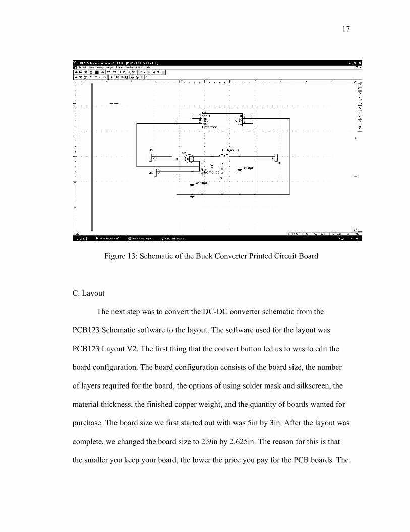
schematic. See Figure 13 to see the Printed Circuit Board Schematic.
17
Figure 13: Schematic of the Buck Converter Printed Circuit Board
C. Layout
The next step was to convert the DC-DC converter schematic from the
PCB123 Schematic software to the layout. The software used for the layout was
PCB123 Layout V2. The first thing that the convert button led us to was to edit the
board configuration. The board configuration consists of the board size, the number
of layers required for the board, the options of using solder mask and silkscreen, the
material thickness, the finished copper weight, and the quantity of boards wanted for
purchase. The board size we first started out with was 5in by 3in. After the layout was
complete, we changed the board size to 2.9in by 2.625in. The reason for this is that
the smaller you keep your board, the lower the price you pay for the PCB boards. The
18
number of layers we used was two and we selected the option of using solder mask
and silk screen. As for the material thickness, we kept the default value of 0.062”.
The finished copper weight we used was 1-oz and the quantity of boards we chose
was two. We were not able to use the 2.5-oz weight because we received too many
unfixable errors. The only solution was to use the 1-oz copper weight. For future
generations, we recommend trying to use the 2.5-oz copper weight since it can carry
more current. However, it should be noted that the price increases with increasing the
copper weight. For PCB123 Layout, the minimum number of boards you must
purchase is two, so this illustrates why we bought two boards.
As this completed the board configuration, we manually arranged the
components on the board. Then we ran the ‘Autoroute’ function which automatically
routes all the connections in the net list. Next, using the PCB Trace Width Calculator
website found on Kaha’s Wiki site we were able to calculate the trace widths for the
ground and input traces since the currents reach high limits at these traces [6]. The
trace widths that we calculated came out to be 139mils after inserting an input current
of 20A, temperature rise of 50 deg C, and an ambient temperature of 35 deg C as
suggested by Kaha Sariashvili. Changing the trace widths for your ground trace and
input traces can be done by going to the edit panel on the left side of the PCB123
Layout screen, clicking on Object Hierarchy, and by changing the properties for the
Net ‘Ground’ trace and the Net input trace. After completing this task, we went on to
changing the hole sizes for the components that needed holes. This was done by
looking at the data sheets for each component that needed holes and changed them
19
accordingly. It turned out that this task would not work by just selecting the pin of the
component and simply changing the hole size in the properties menu. This wouldn’t
work because after applying the changes and actually rechecking each component, the
hole sizes were not changed but back to the default value of ‘None’. So, after
contacting PCB123 support, we were told that we actually have to edit the footprint
of the component and then change the hole sizes and save it. This automatically asked
us to update the component changes and we simply clicked ‘Yes’.
Next we ran the design checks by using the function ‘Run DRC’. This brought
upon us various types of errors and warnings. The warnings that came about were the
silkscreen over copper warnings. These were negligible so we just ignored them. The
errors however could not be ignored and had to be fixed. The three types of errors we
received were the Track-To-Track spacing violation, Track-To-Pad spacing violation,
and Pad-To-Pad spacing violation. These errors mainly occurred because of the
increase in the trace widths. The Track-To-Track errors were the easiest ones to fix
but took the longest to fix because the large trace widths interfered in the routing
leading us to rearrange the routes and make vias (connections between layers). The
Track-To-Pad and Pad-To-Pad spacing violations were the harder ones to fix because
after contacting PCB123, we were told to change the Pad Widths. This was too much
trouble and did not work out at all. However, after receiving feedback from the
SuPER meetings, we were finally able to fix these errors by simply tapering the trace
widths near the pins of the components. After completing the layout with no errors,
20
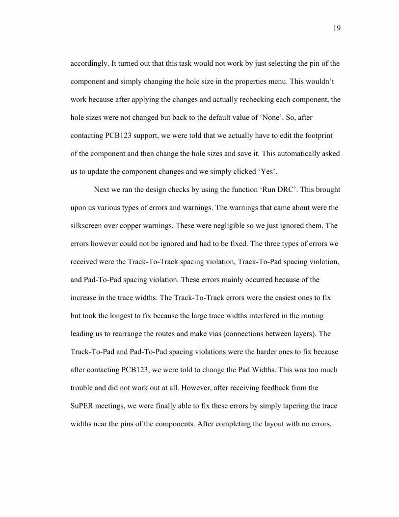
we realized we had assigned the wrong diode part in the Schematic. See Figure 14 to
see our first Printed Circuit Board Layout.
Figure 14: First PCB Layout
This led us to edit the schematic with the correct diode. The diode was
actually a Schottky Barrier Rectifier. It had two anodes and two cathodes. Since this
was a different configuration, the schematic definitely had to be modified. After
completing this task we had to once again find the correct package name. Then we
had to convert this file into the layout again and went through the whole routing
21
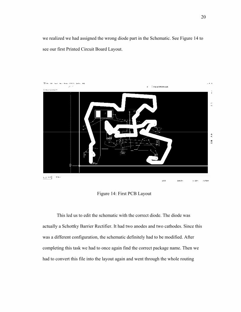
process once again. Finally this task was complete, and the board was ordered. See
Figure 15 for the second Printed Circuit Board Layout.
Figure 15: Second PCB Layout
Refer to the following website for a complete tutorial on the PCB123
Schematic and Layout: http://www.pcb123.com/pcb123tutorial.php. In addition, for
brand new users, the PCB123 website has a downloadable PDF version of the ‘Brand
New Users Guide.’ These tutorials and guides are highly recommended for use by
brand new users of PCB123.
22
V. Construction/Assembly
When we received all our parts and the boards as well, we started out by
trying to see if all the components fit correctly on the board. We realized that this was
a big mistake on our part. We should have rather tested this out by making a one-to-
one printout of the PCB Layout and tested to see if all the components would fit
correctly on paper. So when trying to fit a few of the components on the board, we
realized that there were a few errors. For instance, the terminal blocks would not even
fit onto the board because the spacing of the holes was not correct. The holes were
spaced too closely together. In addition, one of the capacitors fit perfectly, while the
other capacitor did not. The holes were actually too small for the leads of this
capacitor to even fit through. We also came upon a problem with the diode. The three
pin diode holes were not spaced correctly as well. On the other hand, the rest of the
components fit perfectly fine.
Coming upon these errors, we decided to test the high side driver. When
trying to test this chip, we realized that we could not get it to work. This turned out to
be a big problem because in the beginning we were told by Professor Taufik that we
did not need to use the low-side driver part of the chip since the chip was actually a
high side/low side driver. After contacting Texas Instruments, we were told that both
the high side and low side drivers were to be used. This was a big problem because
this told us that we had to make quite a few changes on the PCB Schematic. So in
23
turn, we started editing the schematic. While doing this we realized that there would
be no point in editing the schematic until we got the high side driver chip tested and
working properly to turn the MOSFET on.
In order to test the high side driver chip we used both of the ordered printed
circuit boards and directly soldered the chip where it belonged on the board to test it.
We used long thin wires found in the senior project lab to solder wires to each of the
eight pins. During our testing process however, we kept coming across the problem of
re-soldering the wires back to the pins. The reason for this was because while testing
the chip the pins would get loose and eventually fall off. This resulted in re-soldering
the wires that needed to be re-soldered. We used up both of the boards that we
ordered from PCB123 for testing the high side driver chip but then eventually came to
a conclusion that the whole re-soldering business was really inefficient. This is where
we found out about the SOIC to DIP adapter. The SOIC to DIP adapter was found at
www.ironwoodelectronics.com. You basically take a surface-mount component and
solder it directly on to this adapter. Then you physically take the adapter and stick it
straight into a bread board. This solved the whole problem of repetitive re-soldering
of the wires to each pin. This slowed down our testing process because the order was
supposed to be done by next day air, but Ironwood Electronics is a “Manufacture to
Order” company [7]. They do not stock parts on the shelf due to a high volume of the
different parts that they sell. This basically slowed down the whole process of testing
by more than a week.
24
We received the SOIC-DIP adapter a week after it was shipped. Due to this,
we lost 2 weeks time for testing the high side driver. When we received the adapter,
we were easily able to solder the high side driver onto the adapter. The bottom pins of
the adapter stuck perfectly into the breadboard. This definitely fixed the problem of
re-soldering wires to the chip. This also ended the construction/assembly portion of
our senior project.
25
VI. Testing
In order to make sure the whole buck converter subsystem fully work, we
tested each individual section: high-side driver, inverter, and synchronous buck,
separately. After we finished testing and making sure all the sections were working
the way we expected, we wanted to slowly combine everything. From just the chip,
we include an inverting circuit, then the MOSFETs needed for the synchronous Buck
Converter, and finally the rest of the buck converter.
A. High-Side Driver
Figure 12: Top View of the High-side Driver Chip
Our original design had us using only the high-side portion of the driver to
power a basic Buck Converter. The pins associated with the high-side driver chip can
be seen in Figure 12. After a couple of initial tests and consulting with Texas
Instruments, we learned that we needed to also use the low-side driver to pull down
the circuit and actually turn-off the switch of the Buck converter. The following
26
pages show the tests we ran in chronological order, in an attempt to understand the
high-side driver.
We tried making sure the high-side driver worked the way we expected using
the simple circuit in Figure 13. The idea is the HO (high output) pin would act as a
PWM signal for the MOSFET. When it went high output would equal 0V; when it
went low output would equal 20V.
HO
Output
R1
10k
2
1
M1
20V
Figure 13: Basic HSD and MOSFET Test Circuit
The output resulted in always having a low voltage, 0.437V; in other words,
always tied to ground. At first we thought the MOSFET we were using was acting
up, so we disconnected the HSD and just put two different DC values for the gate
node of the MOSFET to test the MOSFET by itself. Table I shows the test results for
testing the MOSFET.
Table II: MOSFET Test Results
Vg Output 0V 20V 5V 0.437V
27
From that test we concluded that it was not the MOSFET that was acting up
but it was the HSD. It was then that we realized that we did not know how the HSD
chip truly worked. In order to fix this, we spent the next day studying the ucc27201
data sheet and calling Texas Instrument’s Product Information Centers. We learned
that we needed both high-side and low-side drivers in the chip, and the reason why it
was always being pulled down in the earlier test was because the HO pin does not
swing from VCC to ground. The HO pin’s range is from VHS-0.3 to VHB+0.3 [2].
Since HO only operates in a high condition it does not turn off the MOSFET chip.
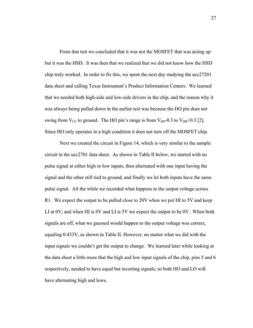
Next we created the circuit in Figure 14, which is very similar to the sample
circuit in the ucc2701 data sheet. As shown in Table II below, we started with no
pulse signal at either high or low inputs, then alternated with one input having the
signal and the other still tied to ground, and finally we let both inputs have the same
pulse signal. All the while we recorded what happens to the output voltage across
R1. We expect the output to be pulled close to 20V when we put HI to 5V and keep
LI at 0V; and when HI is 0V and LI is 5V we expect the output to be 0V. When both
signals are off, what we guessed would happen to the output voltage was correct,
equaling 0.433V, as shown in Table II. However, no matter what we did with the
input signals we couldn’t get the output to change. We learned later while looking at
the data sheet a little more that the high and low input signals of the chip, pins 5 and 6
respectively, needed to have equal but inverting signals; so both HO and LO will
have alternating high and lows.
28
VDD
HO
Q1
MBREAKN
Q2MBREAKN
20V
C1
0.1uF1
2
HB
LOR1
1k
2
1
12V
C2
0.33uF1
2
HS
Figure 14: HSD Testing Circuit
Table III: HSD Testing Data
Trial VDD HI LI HS/output HB VSS 1 12V 0V 0V 0.433 11.46V GND 2 12V 5V 0V 0.428 11.52V GND 3 12V 0V 5V 0.435 11.48V GND
During the next testing session we included a CMOS inverter with the circuit,
but we were still recording the same results. Some time through the test we realized
that the DC voltage source we were using had become current driven and would
immediately reach the current limit we had set to protect our circuit. With the lab
closing and time running out we decided that there has to be something wrong with
our chip since the source would always become current driven. We decided to solder
a new chip to the second PCB board the following day and hoped that this would fix
the problem.
29
We soldered the new chip to the second board, started testing, but the wires
we soldered to board kept coming off and needed re-soldering. After a few more
trials of de-soldering and re-soldering, the old problem of the voltage supply came up
again. As stated in the assembly section, we learned that some how we had shorted
our chip, and in order to continue with the testing we need a better way of accessing
the pins without having to keep re-solder loose wires. A couple of ways we decided
we can fix this are: having a better board - maybe a surface mount or a generic PCB
board; or having a SOIC – DIP adapter. We were not able to find a better board, but
we were able to find an adapter. However there was a delay in the shipping when we
ordered the adapter, which in turn delayed our testing.
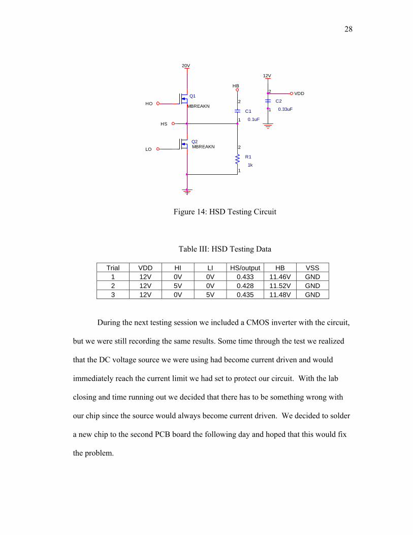
Once the adapter came in the mail, we set up the testing circuit shown in
Figure 15 whereas Table III shows our resulting data. For the first 3 trials we used
the inputs VDD, HI, and LI and recorded the value for every other pin. For trials 4
and 5, we included HS as an input and tied 20V to it. On our 7th trial we started to
run into problems. Earlier, we would have made HI equal 0V and LI equal 5V,
however when we made LI high in the 6th trial, the DC power source we were using
for 12V started to reach the current limit and would not draw the amount of voltage
we wanted as soon as we turn the power supply on. At first this would only happen
when LI was tied high. It would not allow us to even recreate the data from trial 3
and 4. After playing around with the circuit a little more, the same problem started to
occur every single time. No matter what we did the power source would always reach
its current limit instantly.
30
Figure 15: DC Testing Circuit for HSD
Table IV: Data for DC Testing
Trial VDD HI LI HS HB HO LO VSS 1 12V 0V 0V 10.88V 11.16V 10.64V 0.430V GND 2 12V 5V 0V 10.89V 11.17V 10.66V 0.430V GND 3 12V 0V 5V 11.15V 11.16V 10.71V 0.430V GND 4 12V 5V 5V 11.17V 11.17V 10.73V 0.420V GND 5 12V 0V 0V 20V 19.50V 19.60V 0.420V GND 6 12V 5V 0V 20V 19.57V 19.60V 0.450V GND
B. Inverter
After talking to the Texas Instrument technician, it became apparent
that we needed both high-side and low-side drivers used in the chip. In order to do
this the LI and HI inputs need to be opposites of each other. For example when LI is
high, HI would be low and vice versa; we decided to use an inverting circuit as a
hardware solution. We used a CMOS chip - MC14007UB - as seen in Figure 16 from
one of our previous labs to produce an inverting signal.
31
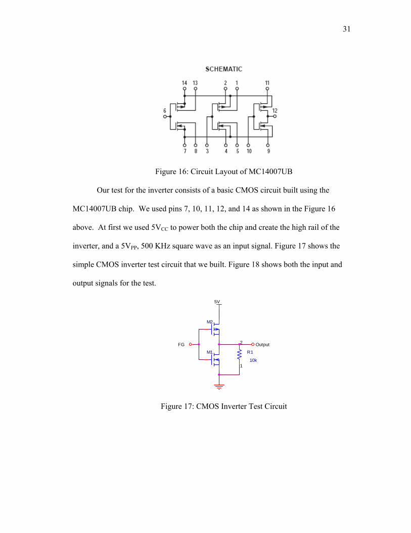
Figure 16: Circuit Layout of MC14007UB
Our test for the inverter consists of a basic CMOS circuit built using the
MC14007UB chip. We used pins 7, 10, 11, 12, and 14 as shown in the Figure 16
above. At first we used 5VCC to power both the chip and create the high rail of the
inverter, and a 5VPP, 500 KHz square wave as an input signal. Figure 17 shows the
simple CMOS inverter test circuit that we built. Figure 18 shows both the input and
output signals for the test.
R1
10k
2
1
FG Output
M1
M2
5V
Figure 17: CMOS Inverter Test Circuit
32
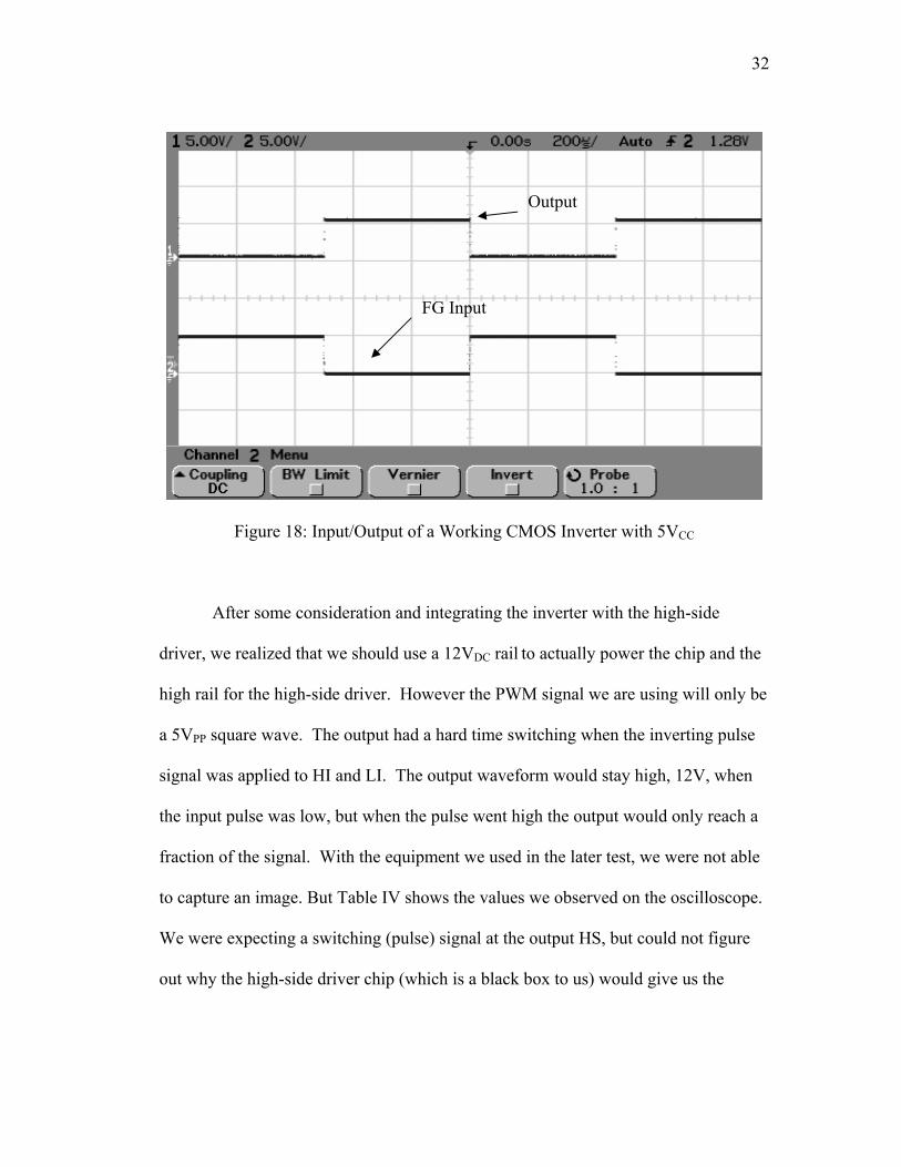
Output
FG Input
Figure 18: Input/Output of a Working CMOS Inverter with 5VCC
After some consideration and integrating the inverter with the high-side
driver, we realized that we should use a 12VDC rail to actually power the chip and the
high rail for the high-side driver. However the PWM signal we are using will only be
a 5VPP square wave. The output had a hard time switching when the inverting pulse
signal was applied to HI and LI. The output waveform would stay high, 12V, when
the input pulse was low, but when the pulse went high the output would only reach a
fraction of the signal. With the equipment we used in the later test, we were not able
to capture an image. But Table IV shows the values we observed on the oscilloscope.
We were expecting a switching (pulse) signal at the output HS, but could not figure
out why the high-side driver chip (which is a black box to us) would give us the
33
unexpected output. Possible corrections to this problem will be discussed in the
conclusion and recommendation section.
Table V: Test Results with Inverter and High-side Driver
VCC FG Output 12V 0V 12V 12V 5V 8V
C. Buck converter
Due to time constraints and lacking various parts we were not able to test the
buck converter. We spent most of our time testing the high side driver to fully
understand how the chip worked.
34
VII. Conclusions and Recommendations
A. Problems and Estimated Completion Time
Since we were not able to get a completed DC-DC converter for our senior
project, there were a few problems that we wanted to address. The problems include
the following: figuring out how to work the high side driver, figuring out why the
power source becomes current driven and getting an inverting circuit for the high side
driver.
The first and foremost problem is figuring out how the high side driver works.
After plenty of testing and consulting, we were still unable to get the results that we
were expecting. The results we were expecting was a pulse width signal at pin HS as
seen in Figure 9. We did contact a Texas Instrument’s technical support
representative and were supposed to get a response within a day or two about why we
were not getting the results we expected. We never received a response from Texas
Instruments so we were basically on our own. In order to solve this problem, we feel
that Texas Instruments needs to be contacted again. Any type of input from Texas
Instruments would be useful in figuring out why our results are incorrect. When
estimating the amount of time that it would take to fix this problem, we came up with
an estimate of 72 hours. We estimated this much time because at least 1-2 days have
to be considered for waiting time to hear back from Texas Instruments. That leaves a
35
minimum of 24 hours for re-testing the circuit according to the input given from
Texas Instruments and getting expected results.
The next problem deals with the power source becoming current driven. In
other words, when testing the high side driver, the circuit would indicate zero voltage
because there was probably a short between the two nodes of the source. As a result, a
new testing method was devised in which we ordered a SOIC to DIP adapter to help
facilitate our testing with such a small chip. It turned out that even with this adapter
we received the same results of the power source becoming current driven. After this
we came to conclude that there has to be something happening internally in the chip
itself. So in order to even understand and fix this problem, we would once again
recommend contacting a Texas Instruments representative and getting feedback on
why such a thing is happening. As for an estimate of how long it would take to fix
this problem in terms of hours, we estimate 72 hours again. This again would give 1-2
days for waiting for a response and 24 hours minimum to re-test the circuit.
The next problem is getting an inverting circuit for the high side driver chip.
We need an inverting circuit because we need a high side and low side input from the
single PWM signal we are receiving from the system. We used a CMOS inverter but
that caused the same problem as mentioned in the paragraph above. In order to fix
this problem, a new inverting circuit needs to be used. Perhaps using an op-amp or
another chip that inverts signals are a couple solution possibilities. As for time needed
to fix this problem, we estimate that it would take approximately 15-20 hours to come
up with an inverting circuit.
36
After all these problems are fixed, the PCB Schematic and Layout are the next
task. The estimated time we feel it would take to complete this task is 10 hours at
most. As soon as the board is completed, you would need to allow at minimum 5 days
for the board to arrive. Then the low power testing needs to be done in order to see if
the circuit works well before moving on to high power testing. We estimate a total of
15 hours maximum for low power testing. The next thing that needs to be done is the
high power testing. This needs to be done because the board needs to be fully tested
before integrating it into the SuPER System. To finish this task we estimate it would
take no longer than 10 hours. This leads us to the next and last task that needs to be
done which is integrating the board into the SuPER system. Keep in mind that system
integration is not simply just hooking up the circuit into the system. Therefore,
system integration would likely take approximately 25-30 hours.
To summarize the minimum total calendar days and person-hours that it
would take to complete this project, it added up to 5 days plus 229 hours. To simplify,
this turns out to be a minimum of 15 full work days (24 hours in a day). It needs to be
noted however that problems are always bound to arise and these numbers are all just
an estimate. It could likely take longer than these hours that we predicted but we feel
it is definitely possible to complete it within the numbers that we chose.
B. Conclusion
Overall, our senior project with the SuPER team has been a tremendous
learning experience. Although we were not successful in building a working Buck
Converter, we learned a lot, first being time management. We realized in order to be
37
successful in any project one must learn how to manage his time properly. If we had
perhaps managed our time in a more efficient manner, we might have accomplished
more than we actually did.
Our requirements for our senior project also kept changing throughout the two
quarters. Since Robert and John were not able to finish building a working Buck
Converter, we could not modify this converter to up the power and build a Cuk
Converter as well. Instead, we were forced to build our own Buck Converter that
would hopefully fit in with the SuPER System. These changes made it hard to focus
on one thing until the end.
Another useful technique we learned had to do with the soldering of the parts.
We learned how to solder accurately and efficiently with extremely small parts. We
also learned how we should be double checking our work for the PCB layout. Buying
boards is not cheap, and so it should be taken into utmost account that the final layout
be as close to perfect as possible. Since our board came with errors, we took it as a
learning experience and moved on with figuring out different ways to test the
converter. Never giving up is a key virtue that goes along with our learning
objectives in the senior project journey.
A few times during our low power testing of the high-side driver, we ran into
a problem where the power source became current driven. In this case, the circuit
would indicate zero voltage because there was probably a short between the two
nodes of the source. As a result, a new testing method was devised in which we had
to order a SOIC to DIP chip to help facilitate our testing with such a small chip.
38
All in all, working on a senior project made us realize that we have to use our
knowledge from all our past Electrical Engineering courses and labs in order to
troubleshoot and complete a successful project. We had to constantly come up with
different test ideas as well as talk with different vendors about certain parts that do
not work as expected. We also realized that when ordering parts or a board, problems
will always arise because things never occur as expected. You never know when
parts will be shipped out – it might take a week even though they say one day.
Problems should always be expected and ready to be handled. Even though we could
not make a successful Buck Converter, we learned a lot through simulation, testing,
time management, and mainly learning about the high-side driver chip which gave us
plenty of problems.
C. Recommendations
When starting the senior project it is essential to research, plan and fully
understand what the project is about. Read over Tyler’s thesis, or at least the
introduction and background, in order to get a good sense of what’s going on with the
whole system. Make a schedule early which has a time table and goal of what you
want to finish each week throughout the two quarters. This will help with time
management, even if you do not follow the schedule exactly; it makes you keep in
mind what you still have to do. The suggestions above will help reduce a lot of time
wasted in the early stages of senior project and less stressful situations during late
stages.
39
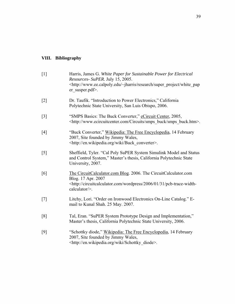
VIII. Bibliography
[1] Harris, James G. White Paper for Sustainable Power for Electrical
Resources- SuPER. July 15, 2005. <http://www.ee.calpoly.edu/~jharris/research/super_project/white_paper_susper.pdf>.
[2] Dr. Taufik. “Introduction to Power Electronics,” California Polytechnic State University, San Luis Obispo, 2006.
[3] “SMPS Basics: The Buck Converter,” eCircuit Center, 2005,
<http://www.ecircuitcenter.com/Circuits/smps_buck/smps_buck.htm>. [4] “Buck Converter,” Wikipedia: The Free Encyclopedia, 14 February
2007, Site founded by Jimmy Wales, <http://en.wikipedia.org/wiki/Buck_converter>.
[5] Sheffield, Tyler. “Cal Poly SuPER System Simulink Model and Status and Control System,” Master’s thesis, California Polytechnic State University, 2007.
[6] The CircuitCalculator.com Blog. 2006. The CircuitCalculator.com Blog. 17 Apr. 2007 <http://circuitcalculator.com/wordpress/2006/01/31/pcb-trace-width-calculator/>.
[7] Litchy, Lori. “Order on Ironwood Electronics On-Line Catalog.” E-mail to Kunal Shah. 25 May. 2007.
[8] Tal, Eran. “SuPER System Prototype Design and Implementation,”
Master’s thesis, California Polytechnic State University, 2006. [9] “Schottky diode,” Wikipedia: The Free Encyclopedia, 14 February
2007, Site founded by Jimmy Wales, <http://en.wikipedia.org/wiki/Schottky_diode>.
40
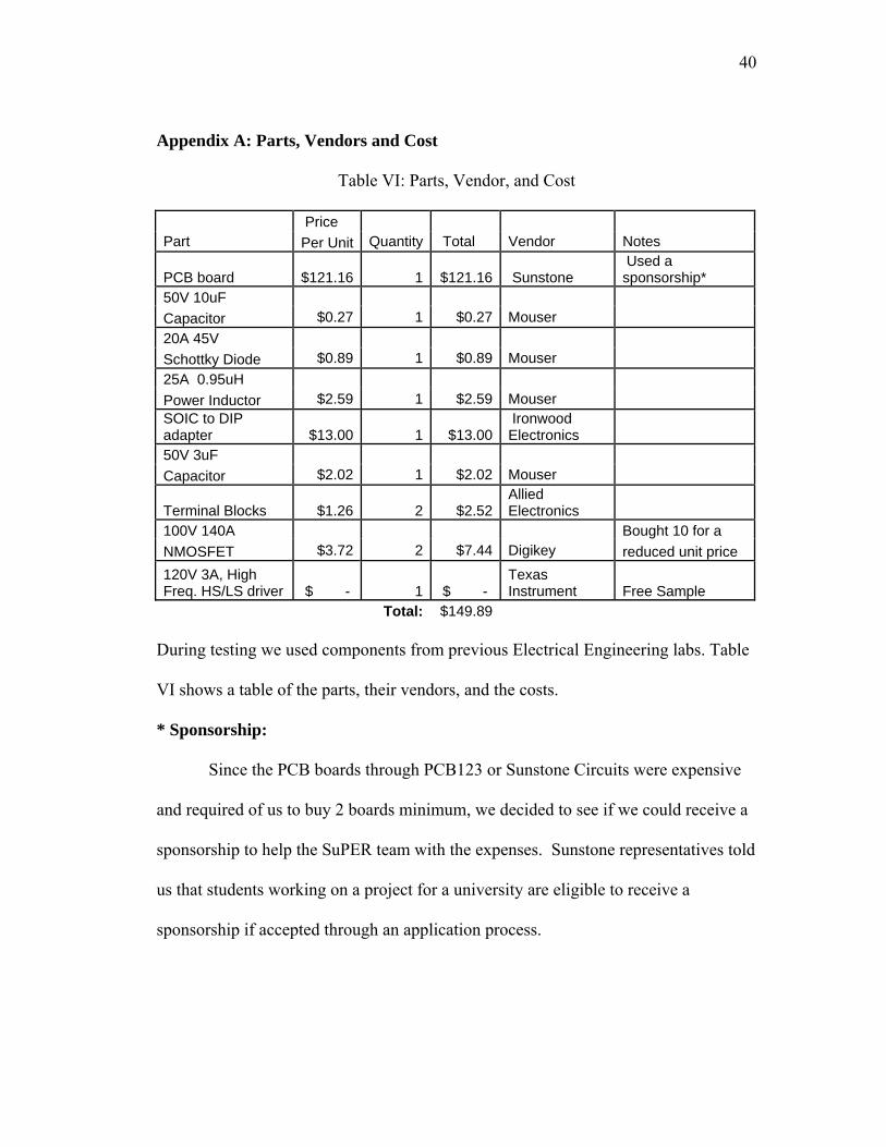
Appendix A: Parts, Vendors and Cost
Table VI: Parts, Vendor, and Cost
Price Part Per Unit Quantity Total Vendor Notes
PCB board $121.16 1 $121.16 Sunstone Used a sponsorship*
50V 10uF Capacitor $0.27 1 $0.27 Mouser 20A 45V Schottky Diode $0.89 1 $0.89 Mouser 25A 0.95uH Power Inductor $2.59 1 $2.59 Mouser SOIC to DIP adapter $13.00 1 $13.00
Ironwood Electronics
50V 3uF Capacitor $2.02 1 $2.02 Mouser
Terminal Blocks $1.26 2 $2.52 Allied Electronics
100V 140A Bought 10 for a NMOSFET $3.72 2 $7.44 Digikey reduced unit price 120V 3A, High Freq. HS/LS driver $ - 1 $ -
Texas Instrument Free Sample
Total: $149.89 During testing we used components from previous Electrical Engineering labs. Table
VI shows a table of the parts, their vendors, and the costs.
* Sponsorship:
Since the PCB boards through PCB123 or Sunstone Circuits were expensive
and required of us to buy 2 boards minimum, we decided to see if we could receive a
sponsorship to help the SuPER team with the expenses. Sunstone representatives told
us that students working on a project for a university are eligible to receive a
sponsorship if accepted through an application process.
41
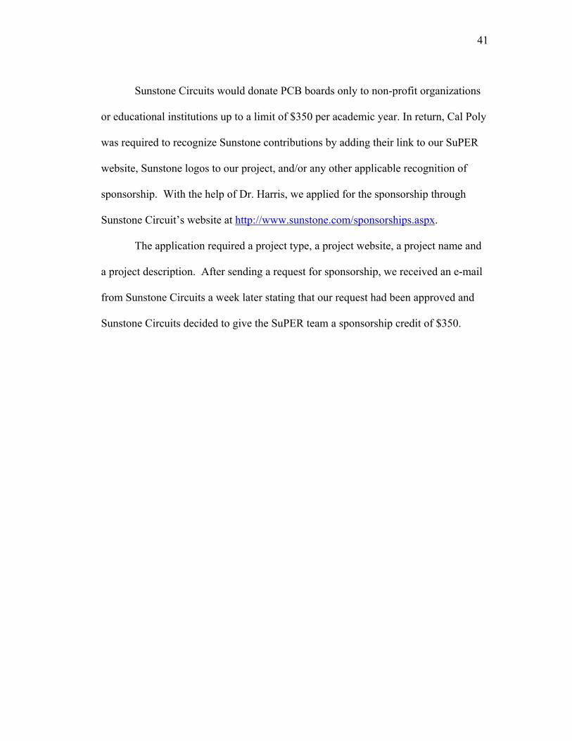
Sunstone Circuits would donate PCB boards only to non-profit organizations
or educational institutions up to a limit of $350 per academic year. In return, Cal Poly
was required to recognize Sunstone contributions by adding their link to our SuPER
website, Sunstone logos to our project, and/or any other applicable recognition of
sponsorship. With the help of Dr. Harris, we applied for the sponsorship through
Sunstone Circuit’s website at http://www.sunstone.com/sponsorships.aspx.
The application required a project type, a project website, a project name and
a project description. After sending a request for sponsorship, we received an e-mail
from Sunstone Circuits a week later stating that our request had been approved and
Sunstone Circuits decided to give the SuPER team a sponsorship credit of $350.
42
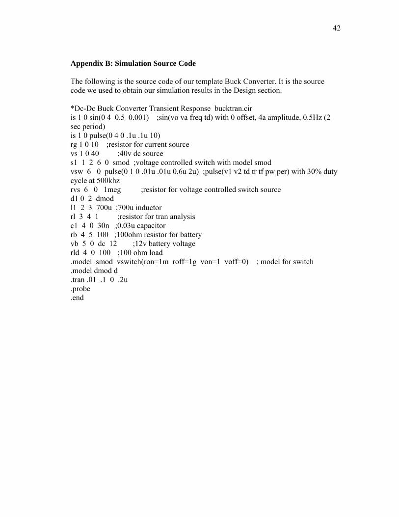
Appendix B: Simulation Source Code The following is the source code of our template Buck Converter. It is the source code we used to obtain our simulation results in the Design section. *Dc-Dc Buck Converter Transient Response bucktran.cir is 1 0 sin(0 4 0.5 0.001) ;sin(vo va freq td) with 0 offset, 4a amplitude, 0.5Hz (2 sec period) is 1 0 pulse(0 4 0 .1u .1u 10) rg 1 0 10 ;resistor for current source vs 1 0 40 ;40v dc source s1 1 2 6 0 smod ;voltage controlled switch with model smod vsw 6 0 pulse(0 1 0 .01u .01u 0.6u 2u) ;pulse(v1 v2 td tr tf pw per) with 30% duty cycle at 500khz rvs 6 0 1meg ;resistor for voltage controlled switch source d1 0 2 dmod l1 2 3 700u ;700u inductor rl 3 4 1 ;resistor for tran analysis c1 4 0 30n ;0.03u capacitor rb 4 5 100 ;100ohm resistor for battery vb 5 0 dc 12 ;12v battery voltage rld 4 0 100 ;100 ohm load .model smod vswitch(ron=1m roff=1g von=1 voff=0) ; model for switch .model dmod d .tran .01 .1 0 .2u .probe .end
43
Appendix C: Analysis of Senior Project Design
Project Title: SuPER System DC-DC Buck Converter
Students’ Names: Thaddeus Guno, Kunal Shah, Koosh Shah
Students’ Signatures:
Advisor’s Name: Dr. James Harris Advisor’s Initials:
Date: June 15, 2007
Summary of Functional Requirements
Our senior project focuses on the implementation of the DC-DC Buck
Converter and its integration with the whole SuPER System. The Buck Converter
provides a physical interface between the solar cell and the battery and loads. It
should be able to handle a wide range of input voltages, ranging from approximately
24V to 40V, and be able to output a voltage ranging from 11.5V to 14V depending on
the battery level. This output voltage along with the power from the battery will
suffice to power the rest of the SuPER System as well as the DC loads.
Primary Constraints
During design and testing, the main constraint we faced was figuring out how
to implement the high-side driver. The high-side driver chip and the erroneous PCB
board made it hard to move on with our project and implement a working DC-DC
Converter. The lack of understanding on how the chip works and consulting Texas
Instrument professionals about it made a big impact on our project. It delayed us
44
from moving forward and was a significant challenge we were not able to accomplish
due to time constraints. Buying new parts to help us out with testing was also another
constraint. Since parts do not ship exactly on time and may take more than a week to
arrive postponed a lot of our testing time. As a result, working efficiently and
allowing more time for parts to come in is a great recommendation for future students
working on their senior projects.
Economic
The original estimated cost for this design was about $100.00. Being a general
estimation, we were not far off from our original estimate. Our total at the end of our
senior project came out to be $149.89. Since we had mistakes in our board, this would
call for a new board. So, since we were not able to complete our DC-DC converter,
the cost for us would have been much higher. However, thinking about it, if our board
was clean, with no mistakes, our general estimate would have been legitimate. We
have to note that mistakes and problems are always bound to occur, therefore possibly
increasing the price of a project. Refer to Appendix A for details on the parts and
costs. As for our estimated development time, we predicted the project to be finished
in about 150 hours. Our actual estimated development time came out to be around
100 hours. Since our DC-DC converter was not complete, we also calculated the
amount of time left in order to finish this project. The calculated calendar days and
person-hours can be seen in the Conclusion section. To summarize, we calculated a
total of 15 (24 hours in a day) full days left to complete the project.
45
Environmental
Our senior project is powered by a photovoltaic source and therefore it should
have negligible effect on the environment.
Manufacturability
Our senior project can be manufactured in the sense that all the components
and the PCB board can be bought from various vendors and put together to build a
Cal Poly made Buck Converter. It would not be cost effective to manufacture all the
components used to make the Buck Converter. However, the PCB board can be
manufactured in the IME laboratory and will cost less than to purchase.
Sustainability
The Buck Converter itself should have a long life cycle; however, the High
Side Driver chip we used does not. After a couple of tests, we were constantly
running into problems with the chip. With this in consideration, it would be highly
beneficial to actually come up with a design that replaces the chip. A couple issues
arise when changing the design of the buck. Among those are the rise and fall time of
the signal that actually goes into the gate of the MOSFET(s) of the Buck Converter.
That time constant needs to be faster than the switching frequency of the PWM
signal. This would ensure the MOSFET(s) will be done switching when the PWM
switches.
Ethical
There are no ethical issues relating to the design of our circuit. We attribute
any help we received to the people who helped us.
46
Health and Safety
There seem to be no health and safety concerns associated with this design.
Social and Political
With the use of the Texas Instrument’s High Side Driver chip, Texas
Instruments would want some recognition with the SuPER project since they supplied
the chip for free as a “free sample.” However, the SuPER team would like the system
to be entirely built from passive parts by Cal Poly students, so we would need to
change the design anyway.
Also, since we received a sponsorship from Sunstone Circuits, in return, Cal
Poly was required to recognize Sunstone contributions by adding their link to our
SuPER website, Sunstone logos to our project, and/or any other applicable
recognition of sponsorship.
Development
A new tool that we used for this design was PCB123 Schematic and Layout.
We learned how to use this software independently and had a good learning
experience using it. Since we were brand new to this software, we used a lot of help
from the visual tutorials and user guides provided by the software providers
(PCB123). We also used the help of a previous user of the software - Kaha
Sariashvili. Overall the experience using this new tool was a good and challenging
one. We would recommend this software to future generations although is not
completely user-friendly. Other alternatives such as AutoCad however would not hurt
and are more than welcome for use.

![DC/DC Converter Reference · 되며, Buck/Boost 회로에도 젂달되어 DC/DC 변환을 위 입력젂원으로도 활용됩니다. [그림 2-1] – SC450의 전원 입력 범위](https://img.pdfslide.tips/doc/110x75/5e4c5ea866d4db1320756c07/dcdc-converter-ee-buckboost-oeeoee-ee-dcdc-e-oe.jpg)