Embed Size (px)
Citation preview
1
The Electronic Properties of Carbon Nanotubes
Philip G. Collins1 and Phaedon Avouris2
1 Department of Physics and Astronomy, University of California, Irvine Irvine, CA 92697-4576, USA [email protected] 2 IBM Research Division, T.J. Watson Research Center Yorktown Heights, NY 10598, USA [email protected]
This chapter provides a broad overview of the electronic properties of carbon nanotubes,
primarily from the point of view of the properties of individual, isolated tubes. The
chapter is organized according to the increasing levels of complexity found in nanotube
electronics. First, the parent material graphite is briefly introduced, followed by a
discussion of the electronic properties of individual, single-walled carbon nanotubes
(SWNTs). Next, the experimentally observed properties of both metallic and
semiconducting SWNTs are discussed in detail. An introduction to many-body effects
and optoelectronic properties of SWNTs is also provided. Towards the end of the
chapter, more complex nanotubes and nanotube aggregates are discussed, since these
types of samples derive many of their characteristics from SWNT properties. The
chapter concludes with a short survey of near-term applications which take advantage of
nanotube electronic properties.
I. Introduction
Carbon nanotubes, first observed by Endo (1, 2), have attracted a great deal of
scientific attention as a unique electronic material. Immediately following Iijima’s
detailed observations (3), theoretical models started appearing predicting unusual
electronic properties for this novel class of materials. Unlike other materials known at
the time, carbon nanotubes were predicted to be either metals or semiconductors based on
the exact arrangement of their carbon atoms (4, 5). At that time, the idea of testing such
predictions seemed fanciful – imaging these wires required the highest resolution
2
transmission electron microscopes (TEMs), after all, and researchers joked about
nanometer-scale alligator clips making the necessary electrical connections.
The jokes were short-lived, of course, as a number of enabling technologies
matured and proliferated throughout the 1990’s and ushered in the new “nanoscience”
field. Scanned probe microscopes (SPMs) became standard laboratory equipment, field-
emission scanning electron microscopes (SEMs) made nanoscale imaging easier than
ever before, and electron-beam lithography brought ultrasmall electronic device
fabrication to hundreds of university campuses. By taking advantage of the long length
of nanotubes, research groups rapidly demonstrated electrical connections to individual
nanotubes and a flood of interesting measurements began.
Historically, the first electrical measurements were performed on multi-walled
nanotubes (MWNTs) (6), nanotubes composed of multiple concentric graphitic shells.
However, the electrical characterization of nanotubes began in earnest in 1996, following
the distribution of single-walled nanotubes (SWNTs) grown by Andreas Thess in Richard
Smalley’s group at Rice University (7). The simpler, single-walled morphology is more
theoretically tractable, and electronic devices composed of SWNTs turn out to be
sufficiently complicated without any additional shells of conducting carbon.
II. Semimetallic Graphite
Graphite is a semimetal, a highly unusual electronic material with a unique Fermi
surface. As a result, the additional quantization present in nanoscale graphitic fragments
is a fascinating subject, resulting in electronic properties which cannot be duplicated by
nanowires composed of normal metals or semiconductors.
Graphite has layered structure composed of parallel planes of sp2-bonded carbon
atoms called “graphene” layers. These layers are 0.34 nm apart and only interact via
weak, van der Waals forces. The quantum electronic states of a graphene sheet are
purely 2D, with nearly continuously varying momenta in the plane (kx, ky), but with only
a single allowed value for kz. This 2D confinement does not in itself lead to deviations
from the standard Fermi liquid model. A nearly free-electron system in 2D has the same
parabolic energy dispersions as a 3D system, though the surfaces of constant energy will
be circles or curved lines instead of the more familiar spheres and spheroids.
3
Figure 1 depicts the 2D bandstructure of a graphene sheet. Many of the constant
energy surfaces in graphene are circular lines, but a notably different geometry occurs at
the high-symmetry corners k = K of the first Brillouin zone. At each corner, two bands*
cross each other with almost perfectly linear dispersion, and the constant-energy surface
shrinks to a discrete point. Quasiparticles on linear bands have no “effective mass” by
standard definitions and may be treated with the Dirac equation for massless fermions.
Because of the crystal symmetry, exactly six points in k-space exhibit this unusual effect,
all having the same magnitude of momentum k = kx2 + ky
2 = π /a , where a is the
hexagonal lattice constant of 0.25 nm. While band-edge states are typically immobile
standing waves centered on the atomic lattice, the graphene states have a nonzero and
nearly energy-independent velocity vF = 8 x 10⁵ m/s.
These unusual features would be easily overlooked if not for the fact that they lie
directly at graphene’s Fermi energy EF, the principal energy of interest for nearly all
electronic properties. Both carbon atoms in the unit cell contribute one delocalized pz
electron to the crystal, so it is perfectly natural for the pz-derived band to each be exactly
filled to the band edge K. This filling sets EF exactly at the band intersection where the
number of available quantum states shrinks to a point. Whereas normal metals might
have spherical Fermi surfaces with many available quantum states, graphene has a Fermi
“surface” composed of only six allowed momenta — more accurately, the surface is a
sparse collection of Fermi points. In can be considered either a very poor metal or a zero-
gap semiconductor.
This low number of states accounts for many of the unusual properties in
graphene-based materials. 3D graphite is categorized as a semimetal (8, 9) and exhibits a
relatively high resistivity ρ ~ 10 mΩ-cm, a nonlinear current-voltage dependence, and an
unusual cusp in the electronic density of states D(E) at E=EF.
III. Single-Walled Carbon Nanotubes
1. Further Quantization of the Graphene System
* The two bands derive from the π states of sp2-bonded carbon. Two π states, one occupied and one unoccupied, result from having two atoms per unit cell.
4
The valence and conduction bands of all materials are drawn as continuous but
are actually composed of closely spaced, discrete states. These states have a regular
separation ∆k inversely proportional to L, the macroscopic length of the sample, and for
large L (compared to the atomic lattice spacing) the states are effectively continuous. For
nanometer-scale materials, ∆k can increase to the point where very few k values are
allowed and the bands of states become quite sparce. Under these conditions, electrons
no longer freely hop from one state to another – the change in either momentum or
energy becomes too great for the available thermal fluctuations – and the material is
considered to be strongly quantized.
Of course, a sample can be quantized in one of its dimensions and not another. A
suitably thin film will retain a continuum of allowed states kx and ky in the plane of the
film, even if only a few, well-separated wavevectors kz remain accessible perpendicular
to the plane. In a nanowire, one of the wavevectors remains quasi-continuous while the
two wavevectors perpendicular to the wire’s longitudinal axis become strongly quantized.
To visualize the available electronic states for a nanoscale 2D film or 1D wire, it often
suffices to extract a plane or a line, respectively, out of the material’s 3D bandstructure.
For a typical metal or semiconductor, this extra quantization rarely results in dramatic
electronic effects: bulk metals tend to produce metallic nanowires, and bulk
semiconductors produce semiconducting nanowires, though with possibly modified
bandgaps.
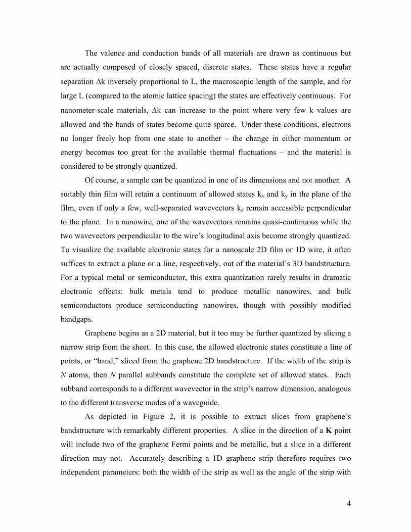
Graphene begins as a 2D material, but it too may be further quantized by slicing a
narrow strip from the sheet. In this case, the allowed electronic states constitute a line of
points, or “band,” sliced from the graphene 2D bandstructure. If the width of the strip is
N atoms, then N parallel subbands constitute the complete set of allowed states. Each
subband corresponds to a different wavevector in the strip’s narrow dimension, analogous
to the different transverse modes of a waveguide.
As depicted in Figure 2, it is possible to extract slices from graphene’s
bandstructure with remarkably different properties. A slice in the direction of a K point
will include two of the graphene Fermi points and be metallic, but a slice in a different
direction may not. Accurately describing a 1D graphene strip therefore requires two
independent parameters: both the width of the strip as well as the angle of the strip with
5
respect to the atomic lattice. Only with both parameters can the electronic properties of
the strip be completely specified.
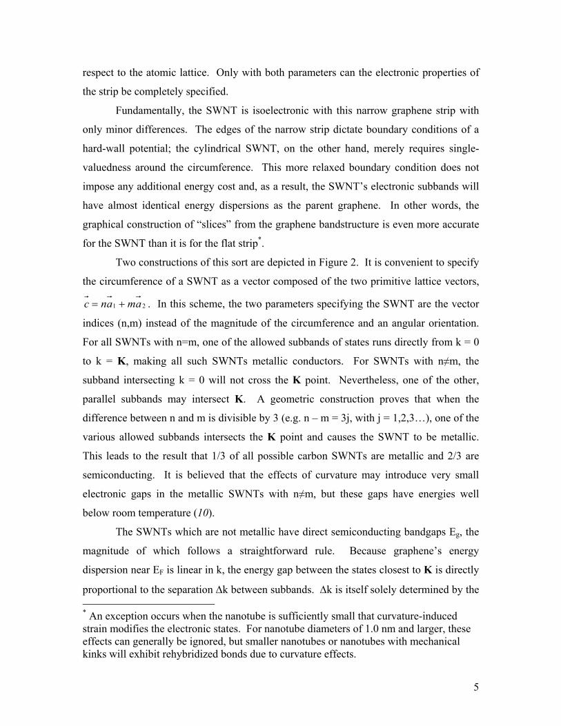
Fundamentally, the SWNT is isoelectronic with this narrow graphene strip with
only minor differences. The edges of the narrow strip dictate boundary conditions of a
hard-wall potential; the cylindrical SWNT, on the other hand, merely requires single-
valuedness around the circumference. This more relaxed boundary condition does not
impose any additional energy cost and, as a result, the SWNT’s electronic subbands will
have almost identical energy dispersions as the parent graphene. In other words, the
graphical construction of “slices” from the graphene bandstructure is even more accurate
for the SWNT than it is for the flat strip*.
Two constructions of this sort are depicted in Figure 2. It is convenient to specify
the circumference of a SWNT as a vector composed of the two primitive lattice vectors,
21 amanc += . In this scheme, the two parameters specifying the SWNT are the vector
indices (n,m) instead of the magnitude of the circumference and an angular orientation.
For all SWNTs with n=m, one of the allowed subbands of states runs directly from k = 0
to k = K, making all such SWNTs metallic conductors. For SWNTs with n≠m, the
subband intersecting k = 0 will not cross the K point. Nevertheless, one of the other,
parallel subbands may intersect K. A geometric construction proves that when the
difference between n and m is divisible by 3 (e.g. n – m = 3j, with j = 1,2,3…), one of the
various allowed subbands intersects the K point and causes the SWNT to be metallic.
This leads to the result that 1/3 of all possible carbon SWNTs are metallic and 2/3 are
semiconducting. It is believed that the effects of curvature may introduce very small
electronic gaps in the metallic SWNTs with n≠m, but these gaps have energies well
below room temperature (10).
The SWNTs which are not metallic have direct semiconducting bandgaps Eg, the
magnitude of which follows a straightforward rule. Because graphene’s energy
dispersion near EF is linear in k, the energy gap between the states closest to K is directly
proportional to the separation ∆k between subbands. ∆k is itself solely determined by the * An exception occurs when the nanotube is sufficiently small that curvature-induced strain modifies the electronic states. For nanotube diameters of 1.0 nm and larger, these effects can generally be ignored, but smaller nanotubes or nanotubes with mechanical kinks will exhibit rehybridized bonds due to curvature effects.
6
width of the graphene strip (or of an unrolled SWNT) and the lattice constant a. So all
SWNTs of a given diameter D will have the same semiconducting bandgap Eg, regardless
of the precise values of n and m, and the value will be Eg = (0.85 eV-nm) / D. Typical
experimental SWNT diameters of 1.0, 1.4, and 2.0 nm give optical bandgaps of
approximately 0.85 eV, 0.60 eV, and 0.43 eV, respectively.
2. Electronic Properties of Metallic Nanotubes
Metallic SWNTs are those which have a subband intersecting the symmetric
Fermi points k = ± K. Each Fermi point contributes one “forward moving” wavevector
with vg > 0 and one “backward moving” wavevector with vg < 0. Including the spin
degeneracy there are exactly 4 forward moving electron states and 4 backward moving
ones at zero temperature.
Each of these states carries current and, in the absence of any scattering, will
contribute one quantum of conductance Go = e2/h = 39 µS. Elastic scattering may be
included in this Landauer model (11, 12) as a non-unity transmission coefficient T, in
which case the total conductance of all four states can be simply stated as
G = Go Σ Ti.
An idealized metal SWNT with four parallel, unity-transmission channels will have a
conductance of 155 µS or a resistance R = 1/G = 6.5 kΩ. This idealized value is not
temperature-dependent.
In a traditional metal, inelastic electron-phonon scattering from acoustic phonons
is the dominant limitation to electrical conductivity, and this scattering limits the
applicability of the Landauer model above. In SWNTs, however, electron-phonon
scattering is strongly suppressed. The 1D electron states of a SWNT can only scatter into
a very limited number of empty electronic states and such events require a large
momentum transfer (13). The resulting suppression produces long inelastic mean free
paths le-ph, on the order of 0.5 µm at room temperature. For submicron-scaled devices,
this means that electron-phonon scattering is essentially absent. In order to
experimentally measure le-ph, on the other hand, devices have been fabricated using
millimeter-length SWNTs (14). As shown in Figure 3, these lengths conclusively
demonstrate the diffusive limit of conduction.
7
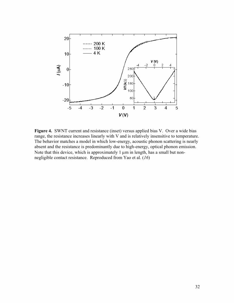
Electron-phonon scattering becomes particularly important at high applied bias
(high fields). As the SWNT bias V is increased, additional scattering mechanisms turn
on and the SWNT resistance increases as shown in Figure 4. This increase is almost
perfectly linear in V, so that the device I-V curve has an apparent current saturation at
high bias. The experimental result is quite counter-intuitive: not only does a metallic
SWNT break Ohm’s law, but it also deviates from the stepwise conductance behavior
normally associated with quantum wires (15). Nevertheless, the behavior is captured by
a simple model of optical phonon emission (16). The suppression of electron scattering
and thermalization by acoustic phonons allows electrons to accumulate energy in an
applied electric field. Once the energy of an optical phonon is exceeded (approx 0.18
eV), spontaneous emission can occur. This dissipative mechanism becomes more active
proportional to increases in V.
The direct observation of optical phonon emission is rarely observed in metals.
Because of the high fields and associated current densities required, most materials will
suffer self-heating and electromigration degradation before a clear phonon emission
regime can be reached. In SWNTs, on the other hand, quasi-ballistic transport is nearly
dissipationless and the covalently bonded carbon atom lattice is impervious to
electromigration. SWNTs readily carry currents of 20 µA, corresponding to current
densities exceeding 108 A/cm2, without degradation. At these currents, the I-V curve
becomes nearly horizontal: the current saturates as all bias increases are efficiently
converted to optical phonon emissions. Higher currents can only be reached by
suppressing this emission, for example by using extremely short devices. The mean free
path for electron-optical phonon scattering in metallic nanotubes has been experimentally
measured to be approximately 10 nm (17, 18), and devices fabricated on this length scale
can carry many times more current.
In experimental SWNT devices, other mechanisms can also play significant roles
and result in low-bias conductances much smaller than 4Go. Contact resistance plagued
early SWNT measurements, limiting measured conductances to 1 – 10% of the
theoretical value. Organic residues from solution-deposited SWNTs and polymer
residues from lithographic processing were two common contaminants at contact
interfaces. Processing improvements have allowed contact resistances to drop
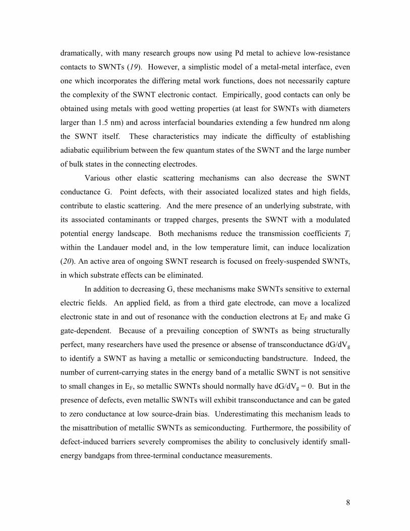
8
dramatically, with many research groups now using Pd metal to achieve low-resistance
contacts to SWNTs (19). However, a simplistic model of a metal-metal interface, even
one which incorporates the differing metal work functions, does not necessarily capture
the complexity of the SWNT electronic contact. Empirically, good contacts can only be
obtained using metals with good wetting properties (at least for SWNTs with diameters
larger than 1.5 nm) and across interfacial boundaries extending a few hundred nm along
the SWNT itself. These characteristics may indicate the difficulty of establishing
adiabatic equilibrium between the few quantum states of the SWNT and the large number
of bulk states in the connecting electrodes.
Various other elastic scattering mechanisms can also decrease the SWNT
conductance G. Point defects, with their associated localized states and high fields,
contribute to elastic scattering. And the mere presence of an underlying substrate, with
its associated contaminants or trapped charges, presents the SWNT with a modulated
potential energy landscape. Both mechanisms reduce the transmission coefficients Ti
within the Landauer model and, in the low temperature limit, can induce localization
(20). An active area of ongoing SWNT research is focused on freely-suspended SWNTs,
in which substrate effects can be eliminated.
In addition to decreasing G, these mechanisms make SWNTs sensitive to external
electric fields. An applied field, as from a third gate electrode, can move a localized
electronic state in and out of resonance with the conduction electrons at EF and make G
gate-dependent. Because of a prevailing conception of SWNTs as being structurally
perfect, many researchers have used the presence or absense of transconductance dG/dVg
to identify a SWNT as having a metallic or semiconducting bandstructure. Indeed, the
number of current-carrying states in the energy band of a metallic SWNT is not sensitive
to small changes in EF, so metallic SWNTs should normally have dG/dVg = 0. But in the
presence of defects, even metallic SWNTs will exhibit transconductance and can be gated
to zero conductance at low source-drain bias. Underestimating this mechanism leads to
the misattribution of metallic SWNTs as semiconducting. Furthermore, the possibility of
defect-induced barriers severely compromises the ability to conclusively identify small-
energy bandgaps from three-terminal conductance measurements.
9
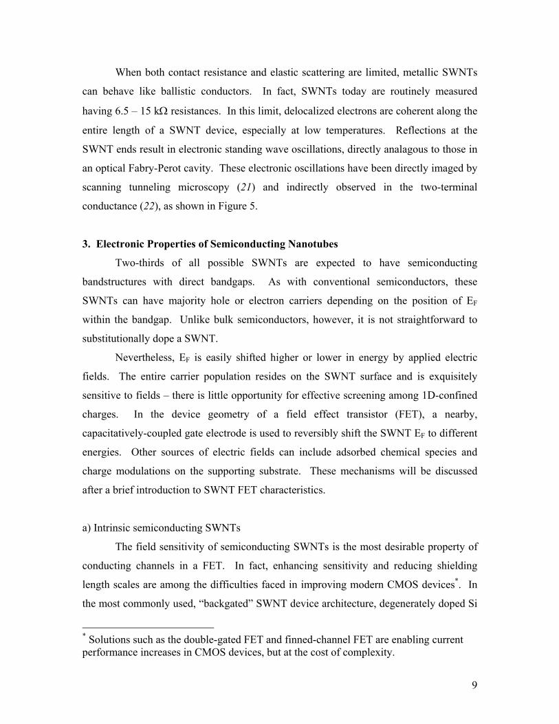
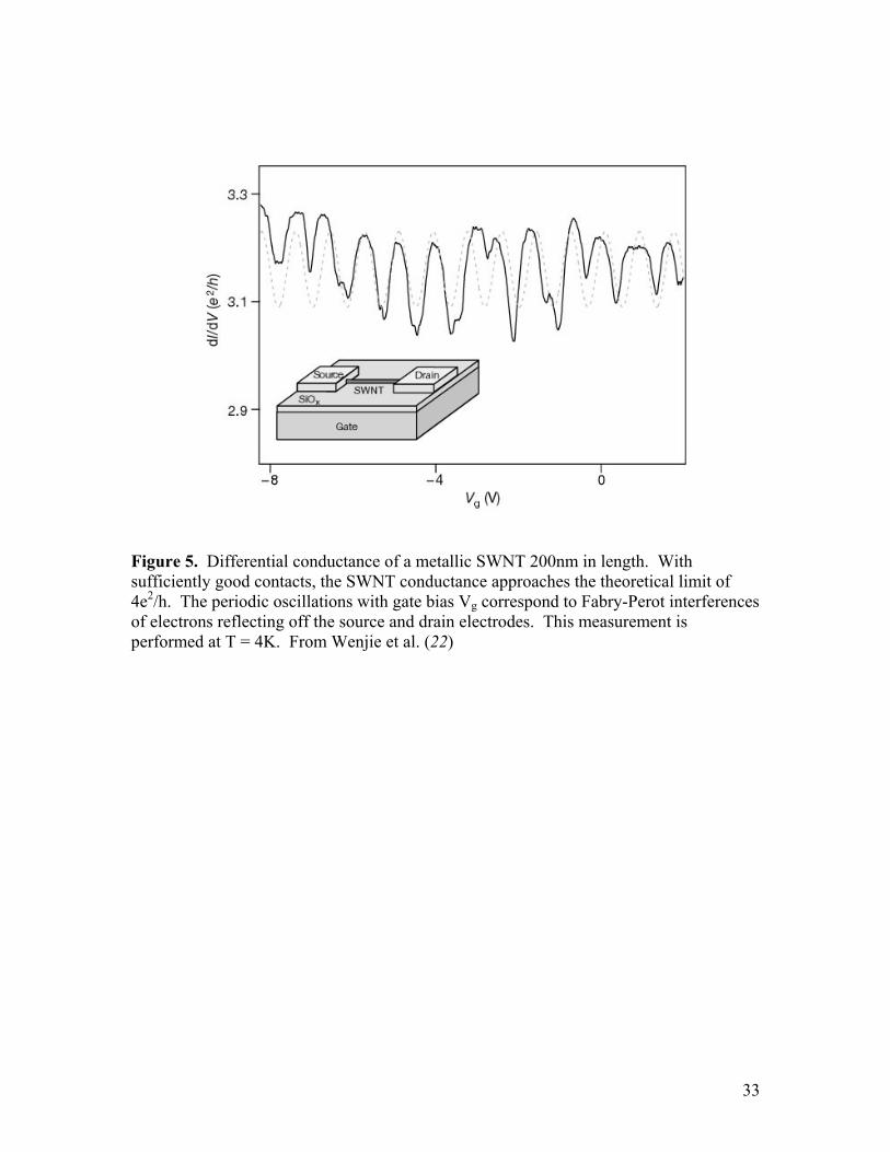
When both contact resistance and elastic scattering are limited, metallic SWNTs
can behave like ballistic conductors. In fact, SWNTs today are routinely measured
having 6.5 – 15 kΩ resistances. In this limit, delocalized electrons are coherent along the
entire length of a SWNT device, especially at low temperatures. Reflections at the
SWNT ends result in electronic standing wave oscillations, directly analagous to those in
an optical Fabry-Perot cavity. These electronic oscillations have been directly imaged by
scanning tunneling microscopy (21) and indirectly observed in the two-terminal
conductance (22), as shown in Figure 5.
3. Electronic Properties of Semiconducting Nanotubes
Two-thirds of all possible SWNTs are expected to have semiconducting
bandstructures with direct bandgaps. As with conventional semiconductors, these
SWNTs can have majority hole or electron carriers depending on the position of EF
within the bandgap. Unlike bulk semiconductors, however, it is not straightforward to
substitutionally dope a SWNT.
Nevertheless, EF is easily shifted higher or lower in energy by applied electric
fields. The entire carrier population resides on the SWNT surface and is exquisitely
sensitive to fields – there is little opportunity for effective screening among 1D-confined
charges. In the device geometry of a field effect transistor (FET), a nearby,
capacitatively-coupled gate electrode is used to reversibly shift the SWNT EF to different
energies. Other sources of electric fields can include adsorbed chemical species and
charge modulations on the supporting substrate. These mechanisms will be discussed
after a brief introduction to SWNT FET characteristics.
a) Intrinsic semiconducting SWNTs
The field sensitivity of semiconducting SWNTs is the most desirable property of
conducting channels in a FET. In fact, enhancing sensitivity and reducing shielding
length scales are among the difficulties faced in improving modern CMOS devices*. In
the most commonly used, “backgated” SWNT device architecture, degenerately doped Si
* Solutions such as the double-gated FET and finned-channel FET are enabling current performance increases in CMOS devices, but at the cost of complexity.
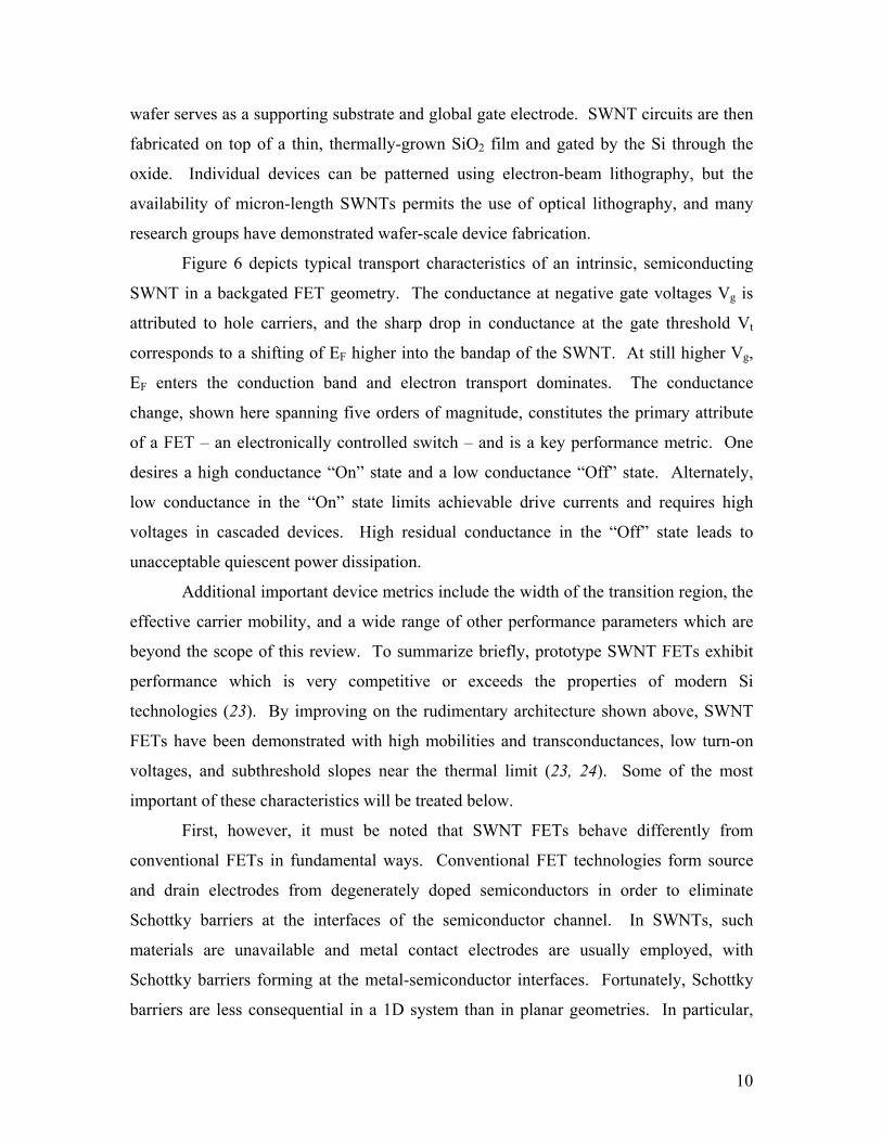
10
wafer serves as a supporting substrate and global gate electrode. SWNT circuits are then
fabricated on top of a thin, thermally-grown SiO2 film and gated by the Si through the
oxide. Individual devices can be patterned using electron-beam lithography, but the
availability of micron-length SWNTs permits the use of optical lithography, and many
research groups have demonstrated wafer-scale device fabrication.
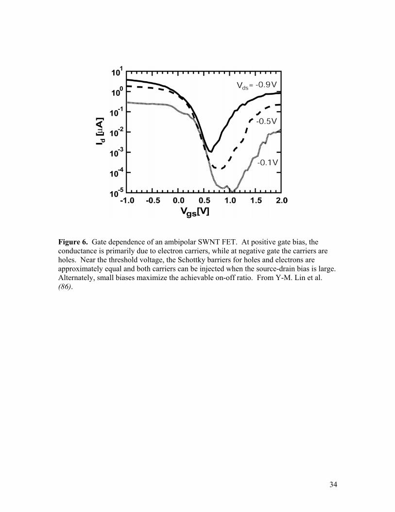
Figure 6 depicts typical transport characteristics of an intrinsic, semiconducting
SWNT in a backgated FET geometry. The conductance at negative gate voltages Vg is
attributed to hole carriers, and the sharp drop in conductance at the gate threshold Vt
corresponds to a shifting of EF higher into the bandap of the SWNT. At still higher Vg,
EF enters the conduction band and electron transport dominates. The conductance
change, shown here spanning five orders of magnitude, constitutes the primary attribute
of a FET – an electronically controlled switch – and is a key performance metric. One
desires a high conductance “On” state and a low conductance “Off” state. Alternately,
low conductance in the “On” state limits achievable drive currents and requires high
voltages in cascaded devices. High residual conductance in the “Off” state leads to
unacceptable quiescent power dissipation.
Additional important device metrics include the width of the transition region, the
effective carrier mobility, and a wide range of other performance parameters which are
beyond the scope of this review. To summarize briefly, prototype SWNT FETs exhibit
performance which is very competitive or exceeds the properties of modern Si
technologies (23). By improving on the rudimentary architecture shown above, SWNT
FETs have been demonstrated with high mobilities and transconductances, low turn-on
voltages, and subthreshold slopes near the thermal limit (23, 24). Some of the most
important of these characteristics will be treated below.
First, however, it must be noted that SWNT FETs behave differently from
conventional FETs in fundamental ways. Conventional FET technologies form source
and drain electrodes from degenerately doped semiconductors in order to eliminate
Schottky barriers at the interfaces of the semiconductor channel. In SWNTs, such
materials are unavailable and metal contact electrodes are usually employed, with
Schottky barriers forming at the metal-semiconductor interfaces. Fortunately, Schottky
barriers are less consequential in a 1D system than in planar geometries. In particular,
11
the electrostatics of a 1D SWNT contacting a 3D metal electrode allow the depletion
widths to vary considerably with applied biases (25). Furthermore, interface states do not
pin the Fermi level very effectively, the way they do in planar interfaces, because of the
lack of screening in 1D. As a result of these differences, SWNT Schottky barriers are
quite sensitive to local electric fields and, in general, the switching in a SWNT FET can
be attributed to Schottky barrier modulation (25, 26).
Much of the literature on SWNT FETs can be fit by a simple model dominated by
Schottky barrier switching. Near Vg = 0, an intrinsic SWNT will be insulating with a
midgap Fermi level EF. Small, negative Vg values shift EF towards the valence band, but
conduction remains limited by a large-width Schottky barrier. As Vg becomes more
negative, the barrier width decreases and hole conductance increases exponentially. The
same occurs for electron carriers at positive Vg. When a work-function mismatch is
present at the interface, the bands have additional curvature at zero gate which can
exponentially favor one carrier type over another. A review of SWNT Schottky barriers
has been presented by Heinze et al (27).
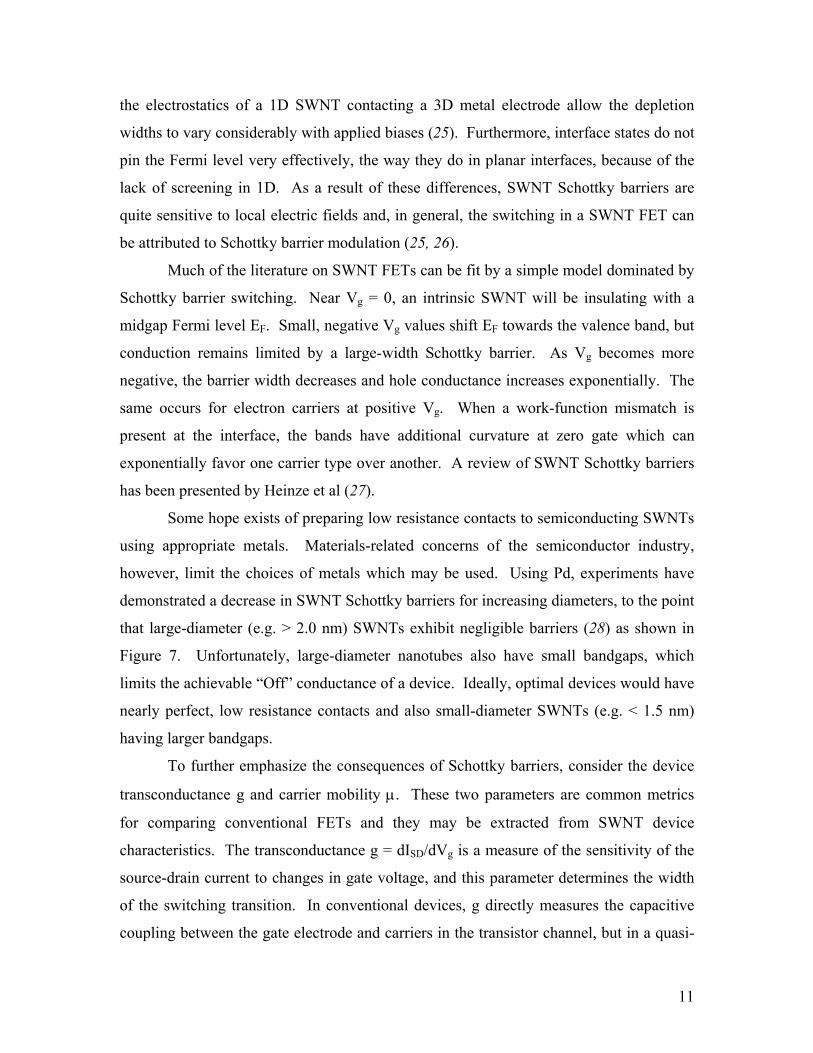
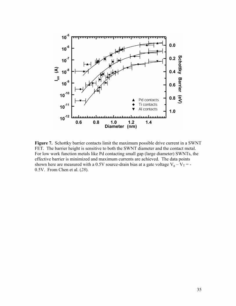
Some hope exists of preparing low resistance contacts to semiconducting SWNTs
using appropriate metals. Materials-related concerns of the semiconductor industry,
however, limit the choices of metals which may be used. Using Pd, experiments have
demonstrated a decrease in SWNT Schottky barriers for increasing diameters, to the point
that large-diameter (e.g. > 2.0 nm) SWNTs exhibit negligible barriers (28) as shown in
Figure 7. Unfortunately, large-diameter nanotubes also have small bandgaps, which
limits the achievable “Off” conductance of a device. Ideally, optimal devices would have
nearly perfect, low resistance contacts and also small-diameter SWNTs (e.g. < 1.5 nm)
having larger bandgaps.
To further emphasize the consequences of Schottky barriers, consider the device
transconductance g and carrier mobility µ. These two parameters are common metrics
for comparing conventional FETs and they may be extracted from SWNT device
characteristics. The transconductance g = dISD/dVg is a measure of the sensitivity of the
source-drain current to changes in gate voltage, and this parameter determines the width
of the switching transition. In conventional devices, g directly measures the capacitive
coupling between the gate electrode and carriers in the transistor channel, but in a quasi-
12
ballistic, Schottky-barrier FET g is wholly determined by the gate’s modification of the
barrier width. Therefore, the measured SWNT transconductance of 10-20 µS (24, 29)
misrepresents the device physics if it is interpreted conventionally. Similarly, the
mobility µ is a measure of the conductivity per individual charge carrier, and in
conventional FETs it is a measure of the carrier velocity (per unit of applied field). In a
quasi-ballistic FET the SWNT mobility is an “effective mobility” in the sense that it does
not merely reflect carrier velocity but also the tunneling characteristics of the Schottky
barriers. In long SWNTs where the bulk scattering dominates and the transport is
diffusive, the mobility has its conventional meaning and values as high as µ ~ 100,000
cm2/Vs have been reported at low fields and room temperature. Theory predicts a
temperature- and diameter-dependence of the low-field mobility (30).
The high performance of SWNT FETs is therefore both an opportunity and a
challenge, since device development must account for their unusual physics. Already,
there is a growing appreciation that these FETs exhibit different scaling rules with respect
to channel length and oxide thickness than traditional devices. Novel architectures have
demonstrated a variety of performance improvements (24, 29, 31, 32), and investigations
of high-frequency behavior indicate that SWNTs may operate at competitive switching
speeds exceeding 100 GHz.
b) Doping & Chemical Variability in Semiconducting SWNTs
Throughout the early years of silicon transistor research, the presence of
unintentional contaminants and dopants complicated and confused experimental efforts.
It is not surprising, then, that similar effects have occurred in the SWNT field.
Throughout the early literature on SWNT FETs, for example, researchers observed only
p-type conduction and no conduction at large, positive Vg (33, 34).
Substitutional doping of the SWNTs seemed unlikely, so other mechanisms were
proposed to explain this p-type behavior. Ultimately, the SWNT devices were
understood to be very sensitive to weakly adsorbed species at or near the Schottky barrier
contact, to the extent that simple air exposure was sufficient to cause the apparent SWNT
doping. Through a gradual discovery process, a wide range of doping experiments and
13
theoretical calculations were performed. As a result, the remarkable chemical sensitivity
and variability of SWNT circuits is now widely appreciated.
Early doping experiments focused on common graphite intercalants such as iodine
and alkali metals, partly in hope of finding superconductivity like in the carbon
fullerenes. Instead of superconductivity, though, researchers found irreversible electronic
behaviors which seemed strongly dependent on sample history (35). The onset of n-type
conduction, which might be attributed to alkali metal intercalation, was not reversible in
vacuum but immediately disappeared upon exposure to air. Subsequently, it was found
that a vacuum treatment alone was sufficient to change the majority carrier type, even in
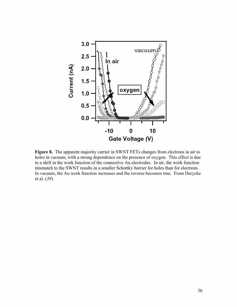
the absence of intentional dopants (36-39).
The net result is that SWNT FETs prepared in air will generally exhibit p-type
behavior, and that vacuum degassing produces n-type behavior. Using intermediate
temperatures, ambipolar behaviors (with EF near the middle of the semiconducting gap)
are also readily obtained. Encapsulation of the devices inside a passivation layer does not
interfere with this thermal treatment, so air-stable devices with either carrier type can be
selected. The effect is shown in Figure 8 for a sample contacted by Au electrodes, and
can be explained in terms of the differing Schottky barrier heights for electron and hole
conduction. The work function of Au, like many metals, is very sensitive to molecular
adsorbates, and these can raise or lower the effective barriers to carriers in a particular
band. The observed p-type behavior is not, therefore, due to hole doping; instead, it
arises from a nearly transparent Schottky barrier to holes and an insurmountable one for
electrons.
This variability can be considered as either an advantage or a disadvantage for
electronic devices. On one hand, the possibility for simultaneous electron and hole
injection at opposite ends of a SWNT enables a range of electro-optic behaviors to be
described further below. The sensitivity to processing conditions, however, also suggests
a variability which poses difficulties for device manufacturing. One solution to this
variability is to better match the SWNT’s work function with that of the connecting
electrodes (19, 38). In this case, EF is most likely to be midgap and neither carrier is
preferentially selected by processing. A second solution is to use smaller bandgap
SWNTs so that the Schottky barrier effects are minimized (28). SWNTs with 2 nm
14
diameters and even MWNTs are much more likely to exhibit ambipolar conduction than
SWNTs with 1 nm diameters. While bandgap reduction can produce low, symmetric
Schottky barriers, it also results in high FET “Off” currents. To achieve acceptable,
reproducible characteristics, the most effective SWNT devices may ultimately employ a
combination of novel architectures, SWNT diameter selectivity, and choice of materials.
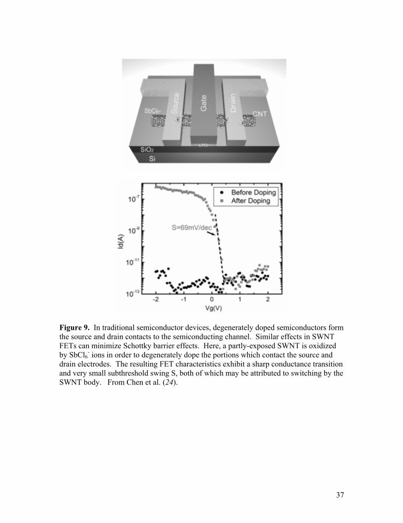
Figure 9 depicts one such architecture in which the ends of the SWNT are degenerately
doped using SbCl6- ions to minimize interfacial barriers.
In addition to these Schottky barrier effects, different molecular species have also
been observed to shift the turn-on threshold VT of SWNT FETs. In this case, the effect is
similar to traditional doping in which EF is shifted higher or lower within the bandgap:
electron donors increase EF and lower the necessary VT for n-type conduction, and
electron acceptors do the opposite. This is most strikingly observed for strong oxidants
and reducing agents like NO2 and amines (40), but it also occurs for a wide range of
reactants including polymers, aromatics, and biomolecules.
The sensitivity of SWNTs is particularly high because these conductors have no
shielded bulk atoms. A single monolayer of adsorbed charge donors approaches a 1:1
atomic ratio with the SWNT carbon atoms, allowing for remarkable dopant
concentrations. Alternately, charge transfer to the substrate and interfaces can also
account for the VT behaviors observed experimentally. A molecule which chemisorbs to
the underlying substrate will produce a local dipole field and partially gate the SWNT.
Since SWNTs have no bulk carriers and are not particularly effective at electrostatic
shielding, this electrostatic local gating is functionally equivalent to the chemical doping
of a particular site. In fact, distinguishing between local electrostatic “doping” and true
charge-transfer to a SWNT is experimentally quite difficult. Different chemical species
may interact with SWNTs through either mechanism.
It is important to again note that this variability has both positive and negative
consequences. Because of the sensitivity of VT to molecular adsorption, SWNT FETs
have been demonstrated as remarkably sensitive chemical sensors. Small, reversible
shifts in VT can lead to orders-of-magnitude change in the FET’s source-drain
conductance at fixed gate bias. On the other hand, before SWNT FETs may be used as
digital logic circuits, this VT variability must be reliably controlled. Recently, progress
15
has been made developing air stable dopants that allow even degenerate doping of
semiconducting nanotubes and thus make possible new device structures that minimize
parasitic capacitances and improve device speed (24).
4. Many-Electron Effects in Carbon Nanotubes
Up to this point, the discussion of the ground state electronic structure and
electrical properties of carbon nanotubes has been based on a single particle, tight-
binding model. While this simple description has been found to be quite successful
overall, it fails to explain many important aspects of nanotube behavior.
Ando and co-workers (41, 42) discussed the role of e-e Coulomb interactions
early on and suggested that they can significantly enlarge the single particle band-gaps in
semiconducting nanotubes, a prediction that was later confirmed by first-principles
calculations (43). The strong e-e interactions, taken in combination with the linear
dispersion near EF in metallic nanotubes, produce a model system for the formation of a
state of matter referred to as a Tomonaga-Luttinger liquid (44, 45). This state is
characterized by unique properties including spin-charge separation and a set of power
laws governing current injection through tunneling contacts.
Experimentally, power law dependences of the differential conductance on
temperature and voltage have been observed in both bundles (46) and individual metallic
SWNTs (47). Furthermore, the power law exponent was found to depend on the
geometry of the contacting electrodes as expected theoretically. The spectral function
and the temperature dependence of the intensity at the Fermi level exhibit power law
dependences with the appropriate exponents when nanotube aggregates are measured by
angle-integrated photoemission (48). All of this evidence supports the Luttinger liquid
model, though conclusive, direct proof awaits future experiments.
Another inadequacy of the single-particle, tight-binding model is an appropriate
description of the excited states of SWNTs. When an electron is promoted to an excited
state, an overall attractive interaction develops between it and the hole left behind to form
a bound state called an exciton. In a perfect 1D system, the electron-hole (e-h) attraction
will be infinite (49). While SWNTs are not quite 1D, e-h attraction leads to the formation
of strongly bound, quasi-1D excitons. The predicted exciton binding energies range from
16
~1eV for small diameter (<1 nm), semiconducting SWNTs, to a few tenths of an eV for
larger (~2 nm) diameter SWNTs (50), with still smaller binding energy excitons occuring
even in metallic SWNTs (50). Another theoretical prediction is that nearly all of the
oscillator strength of the band-to-band transition should be transferred to the exciton,
making the inter-band transition nearly invisible to optical absorption experiments (50).
Three effects have combined to delay the recognition of these important many-
body effects. First, essentially all oscillator strength is concentrated into the excitonic
transition so that only one transition is experimentally observed. Second, the strong e-e
repulsion is partially cancelled by the attractive e-h interaction, so that experimentally
measured excitation energies have reasonably corroborated bandgaps predicted by the
simple, single-particle model. Third, the sharp peaks in photoluminescence spectra have
been favorably compared to the joint density of states arising from van Hove singularities
in the single-particle bandstructure. In fact, these peaks arise from excitonic transitions,
not interband transitions. Only recently has two-photon excitation spectroscopy been
used to confirm the predicted strong excitonic binding in carbon nanotubes (51). The
most important implication of many-body effects is therefore that the optical absorption
(optical band-gap) does not equal the electrical band-gap in semiconducting nanotubes.
This necessitates new types of measurements and the re-interpretation of a number of
transport and optical studies.
An outstanding issue which remains to be addressed in future research involves
the effect of the SWNT’s environment on the above many-body effects. The screening of
e-e and e-h interactions is greatly influenced by the dielectric constant of the surrounding
environment, since the long-range Coulomb fields are primarily transmitted through the
surrounding medium rather than the SWNT body (50). Because of this sensitivity, both
the electrical and the optical bandgaps become environment-dependent. In fact, any
electronic or optoelectronic properties influenced by many-body effects might exhibit
environmental sensitivities.
5. Optoelectronic devices
The combination of electronic and optical properties in semiconductor devices
comprises a broad and important technological subfield. This section deviates from
17
strictly electronic properties in order to address the promise of SWNTs for optoelectronic
devices. It is a mere introduction to a complex and fast-moving field in which many
novel materials have recently attracted attention.
Confined electron and hole carriers can recombine by a variety of different
mechanisms. In most cases, the energy will be released as heat (phonon emission), but a
fraction of the recombination events can result in the radiative emission of a photon. This
process is termed “electroluminescence” and is widely used to produce solid state light
sources such as light emitting diodes (LEDs). In order to fabricate LEDs or any other
electroluminescent device, one must recombine significant populations of electrons and
holes. Conventionally, this is achieved at an interface between a hole-doped and an
electron-doped material (e.g. a “p-n junction”).
Unlike conventional semiconductors, SWNTs can form ambipolar FETs in which
both electrons and holes contribute to the conduction. Using a large source-drain bias,
electrons and holes can be simultaneously injected at the opposite ends of a SWNT
channel. This allows electroluminescence to occur, as first demonstrated by Misewich et
al (52). While the emission mechanism is exactly the same as from p-n junctions,
ambipolar SWNTs do not require chemical doping and formation of metallurgical
interfaces.
Experimentally, SWNT electroluminescence exhibits a variety of interesting
properties. The emitted light is strongly polarized along the tube axis. The radiation also
has a characteristic energy which depends on the diameter and chirality of the excited
SWNT, just as the optical bandgap does. As discussed above, the electronic bandgap is
not necessarily the same as the optical bandgap, since the free electron and hole may first
form a bound exciton before recombining radiatively. Finally, the geometric length of
the electroluminescent region is observed to cover approximately 1 µm. This length may
be interpreted as an effective e-h recombination scale, regardless of whether intermediary
excitonic binding is first occurring.
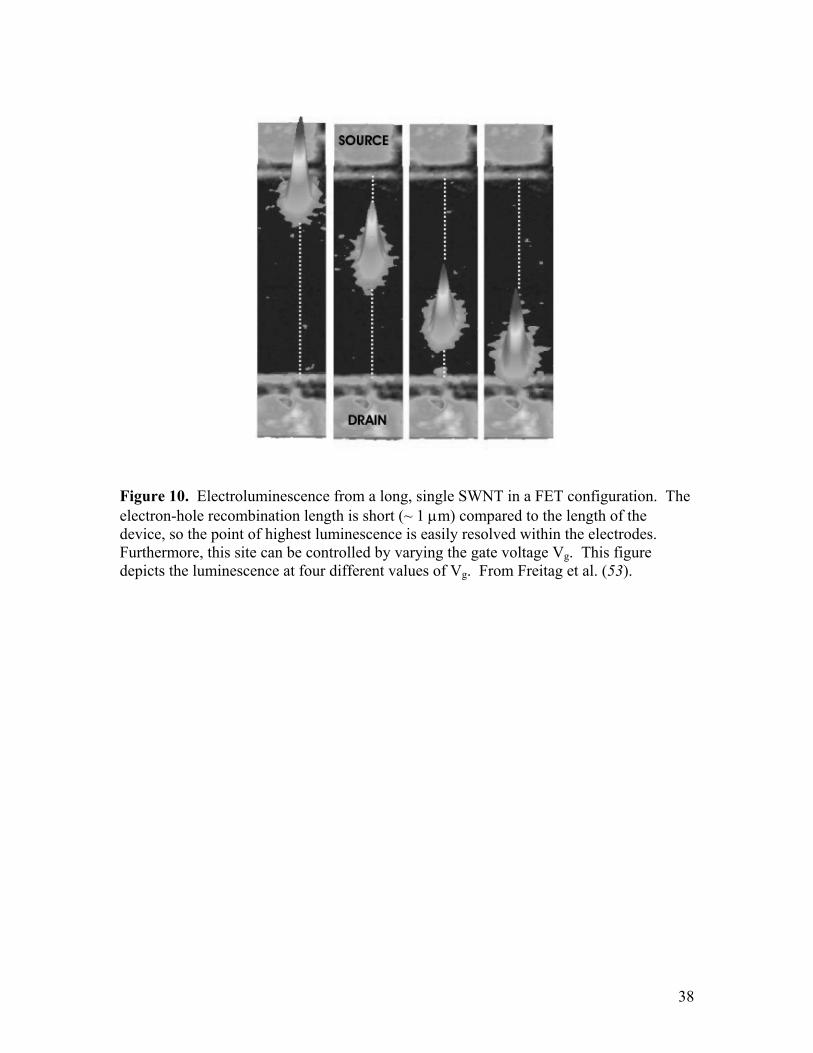
Because this recombination length is relatively long, SWNT devices may be
fabricated either shorter or longer than it. In short SWNT devices, the light emission
encompasses the entire SWNT. In long devices, on the other hand, the emission will be
localized wherever the concentrations of electrons and holes overlap most strongly. This
18
overlap region can be physically moved using a gate electrode, since the relative
contributions of electrons and holes to the total current is strongly gate-dependent. As a
consequence, a SWNT LED is a moveable light source – an electronic signal Vg can
smoothly and continuously position the site of emission (53). Figure 10 demonstrates
this effect for four different gate voltages. One can immediately envision combining
such an LED with an aperture to produce fast electrooptic switches, or electronically
moveable light emitters.
In addition to this translatable emission, localized electroluminescence is also
observed from particular spots on a SWNT under unipolar transport conditions. In this
case, the current is exclusively carried by only one type of carrier, but at certain
randomly-positioned sites light emission is nevertheless observed. Since both types of
carriers are necessary to produce light, these sites must be actively generating e-h pairs.
This process could occur, for example, around SWNT defects, trapped charges in the
insulator, or any other inhomogeneities which produce large, local electric fields. The
monitoring of localized electroluminescence thus provides a potential new tool for
detecting defects in SWNT devices or even large-area device arrays.
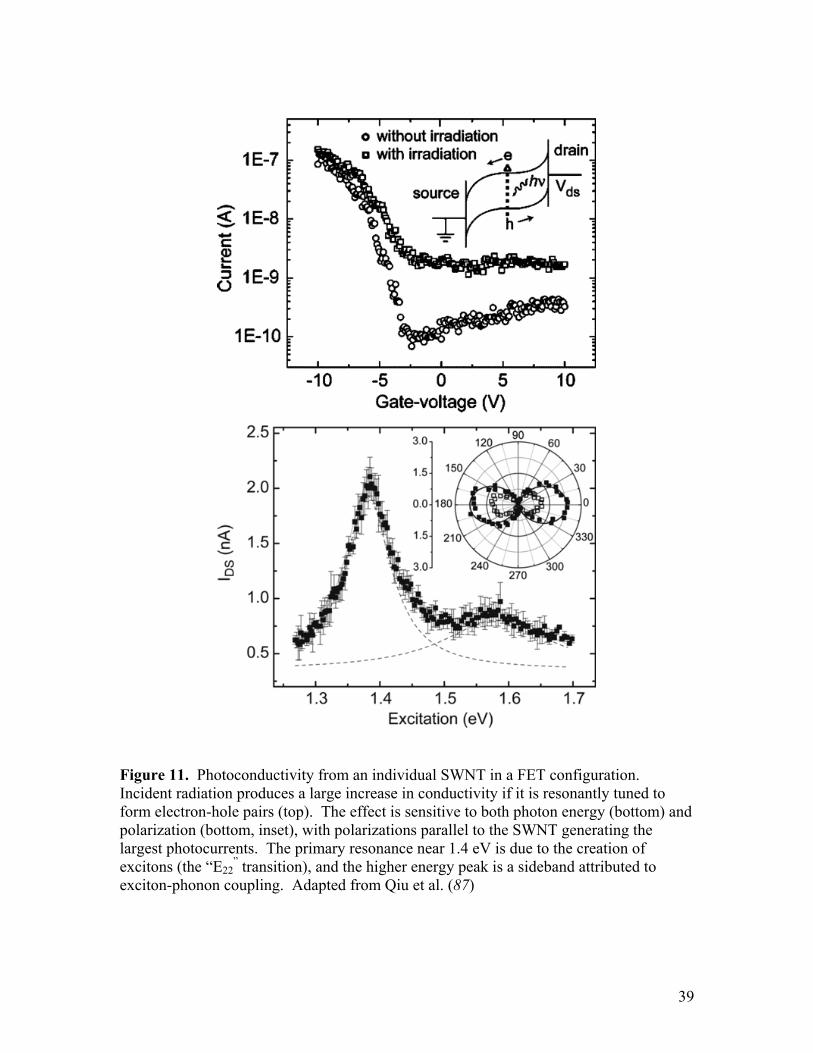
Photoconductivity is the reverse process of electroluminescence, with optical
radiation producing electron and hole carriers. An example of a photoconductivity
measurement is shown in Figure 11. The resonant excitation of a SWNT generates
measureable electric currents with a reasonable photocurrent yield of approximately 10%
(54). Alternately, in the open-circuit configuration the SWNT generates a photovoltage,
which is then limited in magnitude to the SWNT bandgap (54).
Thus, a single SWNT FET device can be used as a transistor, a light emitter, or a
light detector. Choosing among these different modes of operation only requires
changing the bias conditions and does not require separately tailoring the chemical
doping or the device architecture. This flexibility suggests new avenues for SWNT
electronics research, since straightfoward fabrications may be able to produce complex,
SWNT-based circuitry with both digital logic and optoelectronic capabilities.
IV. Carbon Nanotube Aggregates
1. SWNT Ropes
19
While individual SWNTs have now been widely studied, much of the preliminary
nanotube literature from the 1990’s investigated the properties of SWNT “ropes.” These
agglomerations of SWNTs became widely available for electronics research following
the synthesis of Thess et al (7). Because the SWNTs had similar diameters, they close-
packed like threads in a rope and were even briefly considered to be SWNT crystals. The
packing took maximum advantage of van der Waals cohesion and, as a result, made
individual SWNTs quite difficult to experimentally isolate.
Even SWNTs of identical diameter have varied electronic properties due to the
different possible chiralities. A SWNT rope is therefore most simply modeled as a
weakly-interacting bundle of metallic and semiconducting SWNTs in parallel. In reality,
the properties of a rope are somewhat more complex. In large-diameter bundles, only a
fraction of the SWNTs directly contact the connective electrodes, and metallic SWNTs
partially electrostatically shield the semiconducting SWNTs. When the constituent
SWNTs are shorter than the rope itself, conduction must be assisted by intertube
transport. Moreover, the interstitial sites in SWNT ropes can host a wide range of
chemical species. While intercalation may be commercially useful for the storage of
methane gas or lithium ions, both intentional and unintentional doping complicated the
interpretation of early experimental results.
Despite these numerous obstacles, the availability of SWNT ropes accelerated
initial nanotube research. In particular, atomic imaging and spectroscopy by scanning
tunneling microscopy (STM) confirmed the field’s underpinnings (55, 56). Theoretical
models were also refined, with SWNT interactions leading to an additional pseudogap in
D(EF) (10). However, the synthesis of isolated SWNTs by chemical vapor deposition
(CVD) techniques helped overcome many of these materials problems, so that CVD-
grown SWNTs were rapidly adopted as an alternative to SWNT ropes.
2. SWNT Films
By spin-coating or spraying a SWNT suspension onto a substrate, macroscopic
films of SWNTs may be easily fabricated. The primary advantage of these films is their
size, which enabled the earliest attempts to electrically characterize SWNTs. More
recently, interest in both thick and dilute SWNT films has seen a resurgence. Thick
20
SWNT films generally behave like graphitic conductors, albeit with high surface area and
mechanical flexibility. As described in the next section, they have shown particular
promise as electromechanical actuators (57) and as porous electrochemical electrodes
(58) and commercialization efforts are underway using them as microelectromechanical
relays for nonvolatile memory.
Dilute films form percolation networks which, like SWNT ropes, can have
complex electronic properties. Of special interest are networks of sparse SWNTs, which
can be grown using CVD following the dilute dispersal of catalyst particles onto a
substrate. This technique produces a loosely connected film composed of
semiconducting and metallic SWNTs, each of which retains its individual electronic
character. Locally, the electronic properties of such films reflect a parallel combination
of the individual SWNTs. Over large areas, however, the films behave as percolation
networks dependent on SWNT density and length distributions and on the electronic
properties of intertube junctions.
Because semiconducting SWNTs typically outnumber metallic ones by a factor of
two, a regime exists above the percolation threshold in which metallic SWNTs do not yet
fully interconnect. For films in this regime, every conduction path includes one or more
semiconducting segments. These films exhibit remarkably good transistor and chemical
sensor behaviors (59, 60) considering the presence of metallic components. In practice,
the window for fabricating film transistors is not restrictively narrow because SWNT
defects and intertube junctions are also sensitive to electric fields. These additional
transconductance mechanisms relax the restriction on the metallic number density and
have made SWNT film transistors relatively straightforward to fabricate.
Dilute SWNT films have a number of properties which distinguish them from
single-SWNT circuits. They do not have the optimum mobility and subthreshold
characteristcs of individual SWNTs, but as large-area transistors the films exhibit larger
drive currents and have greater tolerance for individual SWNT failures. As demonstrated
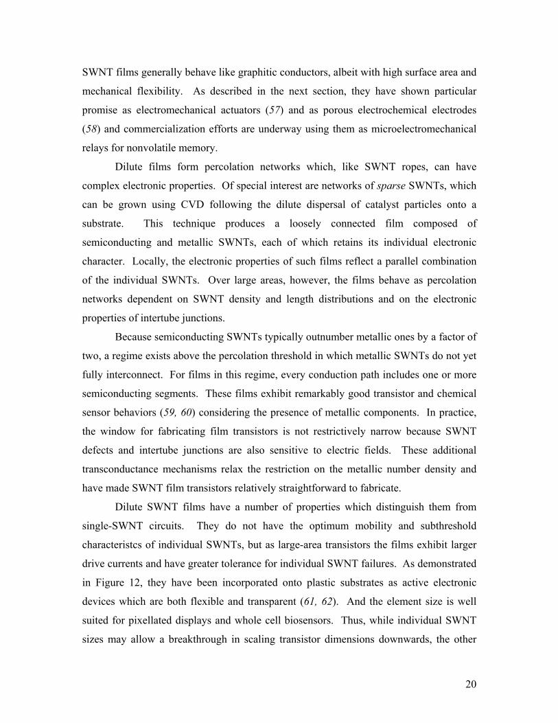
in Figure 12, they have been incorporated onto plastic substrates as active electronic
devices which are both flexible and transparent (61, 62). And the element size is well
suited for pixellated displays and whole cell biosensors. Thus, while individual SWNT
sizes may allow a breakthrough in scaling transistor dimensions downwards, the other
21
unique properties of SWNTs enable a wider range of electronics opportunities, and
research on SWNT films is likely to remain quite active.
3. Multi-walled carbon nanotubes
A multiwalled nanotube (MWNT) consists of individual carbon nanotubes
concentrically nested around each other. Unlike the SWNT aggregates described above,
MWNTs can have a very high degree of order and three-dimensional crystallinity. Each
cylinder, or shell, of the MWNT nests perfectly in the structure with a spacing similar to
the interplanar distance in crystalline graphite. Remarkably, however, the electronic
communication between these shells is minimal. As in graphite, the physical spacing
between layers is 0.34 nm, too large for any significant overlap between the delocalized π
orbitals of adjacent layers. Only defects substantially increase the interlayer coupling,
and interior MWNT layers are believed to have very low defect densities*.
As a result, the individual layers in a MWNT may be modeled as parallel,
independent SWNTs with the properties described above. A rich literature exists on the
possible corrections to this simple model, but to first order it is accurate. Nevertheless,
MWNTs are exceptionally complex wires. The nesting imposes tight restrictions on the
diameter of a particular shell but not on its chirality. Each shell will therefore randomly
alternate between semiconducting and metallic (63), producing something like a coaxial
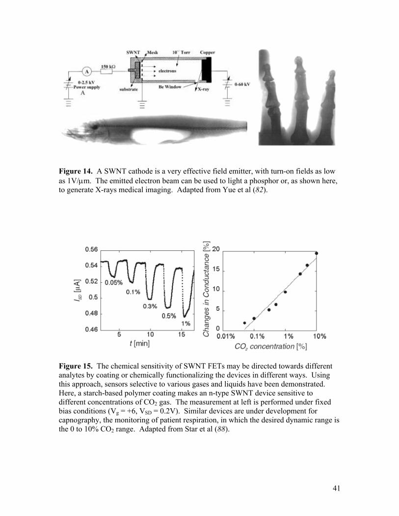
cable but with many more alternating layers. This effect is shown in Figure 13. The
diameter-dependence of SWNT bandgaps is believed to be preserved, so that in the
absence of metallic chiralities MWNTs exhibit a radial bandgap variation from shell to
shell. A typical MWNT might have shell diameters ranging from 2 to 20 nm,
corresponding to electronic bandgaps of 0.3 eV at the inner diameter and 0.03 eV at the
outer surface. At room temperature, therefore, the outer shells of a MWNT conduct
regardless of chirality, since thermal excitations exceed the small bandgaps (i.e. kT > Eg).
A second electronic complication in MWNTs is the existance of closely-spaced
electronic subbands above and below Eg. As depicted in Fig. 2, these subbands have
* Graphite crystals invariably incorporate line and point defects which account for almost all of the c-axis thermal and electrical conductivity, as well as the sample-to-sample variation in these properties.
22
energy spacings of the order of Eg. In SWNTs, Eg is sufficiently large that the subbands
only play a role in optical properties. In MWNTs, on the other hand, these subbands are
merely 10’s of meV apart, so that multiple subbands may be thermally populated at room
temperature. Furthermore, small amounts of chemical doping (64) can shift EF and
ensure that it crosses multiple subbands.
A final complication for MWNT devices is the proper description of their
electrical contacts. For a pristine MWNT physically connnected to a metal electrode,
only the outermost carbon shell is truly connected in an electrical sense. Inner shells are
not ohmically connected but may communicate via tunneling, coulomb drag, diffusive
scattering, and a range of other mechanisms. At low temperatures and low bias, these
mechanisms can be minimized and the measured conductance will be exclusively due to
the properties of the outermost shell. Under these conditions, MWNTs behave very
much like large-diameter SWNTs, with quasi-ballistic conduction, coulomb blockade
charging effects, and even Ahronov-Bohm-like interferences from circumferential states
(65, 66).
At high bias, on the other hand, electron injection at the contacts helps to
equilibriate multiple shells, all of which contribute to conduction with one or more
subbands. Room temperature measurements clearly indicate the contributions of multiple
shells, even in the low bias limit (67). For example, a MWNT composed of an outer
semiconducting shell and an inner metallic shell can be partially gated by electrostatic
fields, but never turned off because of leakage through the metallic component. More
complete characterizations can individually measure every shell’s contribution and
sensitivity to electrostatic gating (63). Despite this facility, the precise behavior of a
given MWNT is difficult to generalize because of the many different types of variability.
Under exceptional conditions, MWNTs can exhibit conductance quantization,
even at room temperature. A series of experiments performed with suspended MWNTs
dipped into liquid mercury contacts has demonstrated characteristics of single-shell
ballistic transport (68, 69). These effects are not observed in planar, lithographically-
fabricated devices, however, even ones in which the MWNT is suspended across an air or
vacuum gap. It may be that unique properties of mercury, combined with a special
23
preparation which eliminates surface scattering, allows the quantization steps to be
observed.
To take full advantage of their inner carbon shells, it is possible to modify a
MWNT in various ways. By chemically etching the ends, all of the MWNT shells can be
exposed and a metal electrode will then contact each one, albiet with a vanishingly small
contact area. Alternately, energetic beams of electrons or atoms can be used to introduce
defects and electrically crosslink the shells (70). At very low dosages, MWNTs become
better conductors due to the contributions of multiple inner shells, but generally the
simultaneous loss of crystallinity degrades the conductivity and introduces disorder
scattering. Such samples then exhibit unusual bias- and temperature-dependences.
4. Disorder in the Nanotube Nomenclature
Because of the rapidly growing literature on nanotube electronics, it is important
to point out that variations exist in carbon nanotube nomenclature. A wide variety of
material morphologies exist, especially given the large number of research groups
investigating nanotube synthesis. The electronic properties described above are unique to
isolated, sp2-bonded planes of graphitic carbon and do not necessarily apply to more
disordered carbonaceous materials.
Two particularly subtle errors frequently mislead researchers unfamiliar with the
historical development of the field. First, a wide range of hollow-core materials have
been called MWNTs. The earliest MWNTs were grown at very high temperatures in arc
furnaces designed for the production and study of fullerenes. High temperatures assist
the annealing of sp2-bonded networks and much of the structural carbon in these
nanotubes was believed to be defect-free, making the graphene bandstructure relevant. In
such materials, the intershell coupling is indeed minimized and the individual shells can
be quasi-ballistic. Theoretical models of MWNTs exclusively refer to such materials.
Experimentally, less crystalline carbon wires such as those synthesized at lower
temperatures can be highly defective and rarely consist of perfectly nested shells, much
less electronically independent ones. These materials generally have the electronic
properties of graphitized carbon fibers, which cannot be reasonably compared to the
single-conducting-shell results (65, 68) described above. A wide range of hollow carbon
24
wires are called MWNTs only by convenience, even though they may clearly lack the
mechanical, chemical, and electronic properties associated with SWNTs and the MWNTs
of theoretical models.
A second comment regards the existing literature on SWNTs. The early synthesis
of SWNTs was achieved by incorporating transition metal catalysts into carbon plasmas.
During the popularization of CVD synthesis, it was therefore widely accepted that
catalyst-promoted nanotube growth resulted in SWNTs. Many experimental results have
been attributed to SWNTs without any structural characterization other than a
measurement of the outer diameter. Subsequently, careful microscopy (71) and shell-
counting experiments have determined that diameter is a very poor predictor of the
number of shells in a CVD-grown nanotube, especially for diameters larger than 2 nm.
True SWNTs with diameters of 1 nm, 2 nm, 3 nm, and higher have indeed been observed
by high resolution microscopy, but double-walled and triple-walled nanotubes are far
more common at the larger diameters and accurate wall counting requires patience and
skill. The unintentional experimental confusion on this issue indicates the lack of
techniques originally available for characterizing nanotubes integrated into electronic
circuits. Today, techniques such as Raman spectroscopy can clearly distinguish between
circuits have single-walled or double-walled nanotubes.
V. Electronic Applications of Carbon Nanotubes
Because nanotubes exhibit many interesting electronic properties, a wide range of
electronic applications have been proposed and investigated. Various prototype devices
have been demonstrated with excellent, commercially-competitive properties.
However, a primary obstacle to many applications remains the variability in
electronic characteristics. Chiral variability is a widely acknowledged problem with
SWNTs, but there is hope that it may be solved through specially designed catalysts or
selective wet chemistry (72). An equally serious but less well-documented problem is the
sensitivity of SWNTs to small chemical, mechanical, and electronic variations present on
substrates, at metal electrodes, and in the SWNTs themselves. Researchers who have
produced 4” and 6” wafers full of SWNT devices have sidestepped the chirality problem
by manually selecting the subgroups of semiconducting or metallic SWNTs. Even
25
among these subgroups, electrical properties vary by an order of magnitude from device
to device, perhaps due to surface contaminants or nanoscale geometric variations. When
the SWNT diameter is not precisely controlled, the variations are even larger.
Thus, even if the chirality issue were immediately resolved, consistent
specifications for nanotube circuitry would remain elusive. SWNT transistors and
memory elements for digital logic can be individually demonstrated but not yet
manufactured, and many additional processing techniques remain to be discovered and
developed before SWNT devices will have reliable data sheets. In this sense, nanotube
electronics resembles early Si research of the 1950’s and 60’s. Variability remains a
primary challenge for nanoelectronics applications in which SWNTs assist downscaling
to ultrasmall or ultradense circuitry.
Larger circuits and devices incorporating many nanotubes can be much less
sensitive to small fluctuations on individual SWNTs. For example, the thin-film SWNT
FETs described above are not particularly small, but their flexibility, reasonable
performance, and low-cost fabrication suggest particular application niches. Similar
electronic devices which rely only on nanotube ensemble properties can be produced
more dependably than single-nanotube devices, and some of these are closer to successful
commercialization. The remainder of this section provides a short tour of potential
applications enabled by the electronic properties of nanotube ensembles. One must
consider, however, whether the performance of these large nanotube ensembles is
distinguishable from that of films of carbon fibers, a more traditional and much lower
cost material.
1. Conductive Composites
Because of their extreme aspect ratios, nanotubes can form conductive percolation
networks at very small volume fractions. By embedding nanotubes into a polymer
matrix, antistatic and electrically conductive plastics are readily produced. In fact, such
products are the earliest-known commercial applications of carbon nanotubes. The
volume fraction of nanotubes can be as small as 0.1% (73), allowing the intrinsic
properties of the matrix, which might include transparency, flexibility, and strength, to be
26
retained. At still higher densities, the nanotubes can also begin to tailor the matrix’s
mechanical properties.
When not confined within a matrix, conductive nanotube films exhibit large
surface areas and significant mechanical flexibility. These properties enable
electrochemical and electromechanical applications (74). For example, nanotube
“supercapacitors” exhibit very large capacitances for their size, because even a
compressed nanotube film remains porous to most electrolytes. A nanotube electrode
with a macroscopic area A has an effective surface area hundreds of times larger than A
and exhibits capacitances exceeding 100 Farads per gram of nanotube material (74).
Furthermore, nanotube supercapacitors can charge and discharge at power rates of 20 –
30 W per gram, sufficient for high power applications such as hybrid-electric vehicles
(75). The chemical inertness of nanotubes is critical to this type of application:
nanotubes do not readily degrade with repeated cycling the way that other high-surface-
area materials do. Of course, some electrolytes are more chemically active than others,
and the application of nanotubes to lithium ion storage has been hampered by large,
irreversible capacitances (76). Nevertheless, nearly all lithium ion batteries manufactured
today include a small percentage of lifetime-enhancing carbon nanotubes. Both
capacitative and chemical energy storage using nanotube electrodes remain active
research topics, with products successfully deployed in both areas. However, these
applications are quite sensitive to the high costs of nanotube materials and will benefit
from ongoing research in bulk nanotube synthesis.
Nanotube films have also been investigated as electronically-controlled
mechanical actuators and switching elements. In an electrolyte, the capacitive charging
of a nanotube film leads to swelling and mechanical deformation (57), which can be
employed as a type of actuator. In air or vacuum, electrostatics alone are sufficient to
deform nanotubes (77), since despite their high tensile strength nanotubes are relatively
floppy and bendable. The deformation of individual nanotubes has been imaged by SEM
and TEM, and using high frequency fields a nanotube’s mechanical resonances can be
directly measured (78, 79).
Visionaries imagine mechanical work at the nanoscale being accomplished by
nanotube actuators and positioners. In the shorter term, electromechanical actuation has
27
been employed to build simpler electronic switches (80). These devices resemble relays
with nanotube films as the flexible armature contact. Unlike relays, these mechanical
switches do not require magnetic fields or power-hungry solenoids, so they can be
lithographically fabricated in large arrays and potentially used for nonvolatile memory
applications.
2. Electron Emitters
As chemically inert wires with high aspect ratios, carbon nanotubes exhibit all of
the properties desired in a good field emitter (81). Both SWNTs and MWNTs exhibit
emission at low threshold electric fields of 1 to 2 V/µm, indicating that their sharp tips
geometrically enhance local electric fields by factors of 1000 or more. The tolerance of
nanotubes for extraordinary current densities further allows these emitters to operate at
high power densities.
Individual field emitters constitute a small commercial market, but arrays of
emitters can be used for general lighting, flat panel displays, and high power electronics.
In each of these applications, the nanotube emission exceeds the minimum performance
specifications to be competitive; the primary barriers to commercialization involve other
issues such as fabrication, compatibility, and product complexity. In lighting, these
barriers are relatively small and high-brightness, high-efficiency lighting products exist.
Alternately, flat panel displays are highly complex products with interrelated technical,
economic, and practical specifications. Display technologies demand thousands of
identical pixels, a stringent requirement on emitter variability. In this field, multiple
demonstration prototypes by companies including Samsung and Motorola have not yet
resulted in consumer products.
Field emission is intrinsically a nondissipative, energy-efficient tunneling process.
Emission devices are therefore useful in a variety of high power density applications,
such as the frequency modulation of very large currents or surge protection for power and
telecommunications substations. In the past, potential power devices such as these have
been severely limited by the available field emission materials, and nanotubes have made
new performance levels possible.
28
Additionally, a field emission beam is very energetic, and when directed at a
metal target it can generate x-rays (82). Before nanotubes, field emission sources lacked
the current densities necessary to produce high flux x-ray sources for medical imaging or
scientific equipment. As a result, x-ray equipment has depended on power-hungry,
water-cooled, thermal electron sources. The advent of nanotube-based x-ray sources
allows low weight, low power, portable devices, with the added advantage of higher
spatial resolution and longer lifetimes compared to thermal sources (82). These devices
are currently being developed for multiple applications including biomedical scanning,
airport security, and space exploration, as depicted in Figure 14.
3. Chemical and Biological Sensors
Chemical and biological sensing constitute a broad market fragmented into many
niches and served by a wide variety of transduction mechanisms – optical,
electrochemical, mechanical, and electronic. Electronic sensors have generally competed
poorly because of the difficulty of interfacing solid state circuits with chemically-specific
functional molecules, and doing so without inducing temperature, humidity, and temporal
variabilities.
In principle, SWNTs are ideal for electronic chemical sensors. Charge carriers
are exclusively confined to the conductor’s surface and the measured resistance can be
sensitive to individual scattering sites. Even though applications requiring large numbers
of identical FETs remain out of reach for SWNT electronics, a chemical sensor demands
only a few individual circuits. Put another way, a chemical sensor can exploit one of the
biggest weaknesses of SWNT circuits, namely their sensitivity to chemical perturbations.
Nevertheless, the very possibility of chemical sensitivity was not appreciated in the early
years of SWNT research. Attempts to intentionally dope individual SWNTs led
researchers to uncover unexpected sensitivities to air exposure and re-evalaute the p-type
behavior of SWNT FETs (36). Subsequent experiments found sensitivities spanning
from reagents like NH3 and NO2 (40) to inert gases (83).
The field of chemical sensing continues to be unique among the electronic
applications described here because it remains poorly understood on a fundamental level.
No single explanation can account for all of the experimental evidence of chemical
29
sensitivity in SWNT circuits. Active hypotheses include chemical doping of SWNTs by
charge transfer, electrostatic doping via charge transfer to the supporting substrate,
modulation of interfacial (Schottky) barriers due to adsorption on the metal electrodes,
chemical modification of defect sites, mechanical impingement and deformation of the
SWNT structure, and simple van der Waals interactions.
Nevertheless, the development of SWNT chemical sensors is progressing
remarkably quickly considering that so little has been confirmed regarding the
transduction mechanisms. Experimentalists have confirmed the effect, tailored its
usefulness, and sensor products are now commercially available. Prototype sensors exist
which can test for dilute toxic gases, hydrogen gas leaks, traces of explosives, and
specific analytes in medical patients’ breath. By extending the principle to SWNT
devices coated with proteins or antibodies, simple biochemical sensors have also been
demonstrated (84). Similar progress with a variety of non-carbon nanowires provide
researchers significant latitude to choose an appropriate surface chemistry for a particular
analyte. The carbon SWNT, however, may provide an optimum starting point for
leveraging organic chemistry. Direct linkages of carbon SWNT circuits into
biomolecular processes is a new research opportunity which is only beginning to be
explored, and the field is likely to grow rapidly in coming years. The concept captures
the broad premise of nanotechnology and suggests that the highest impact applications of
SWNT electronics may result from innovation at the boundaries between solid state
electronics, chemistry, and life sciences.
30
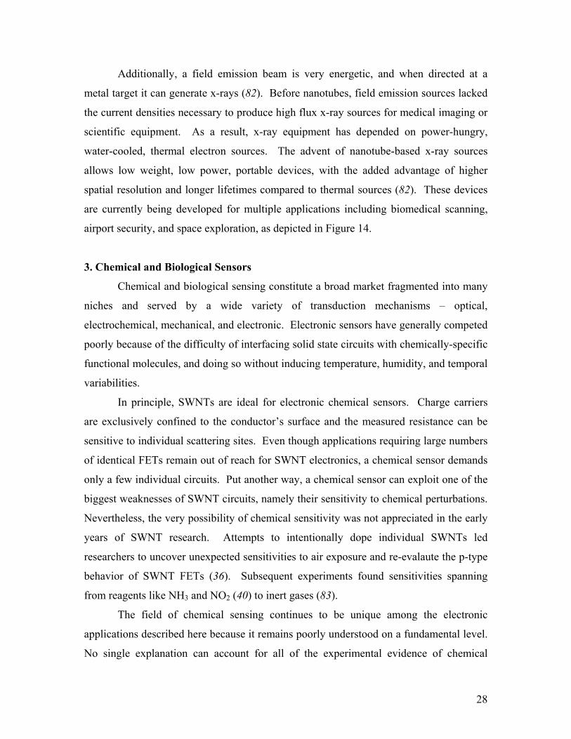
Figure 1. The electronic bandstructure of a graphene sheet has band crossings at the high-symmetry corners K and K’ of the Brillouin zone. The Fermi level EF intersects these crossings, resulting in the semimetallic properties of graphene and graphite.
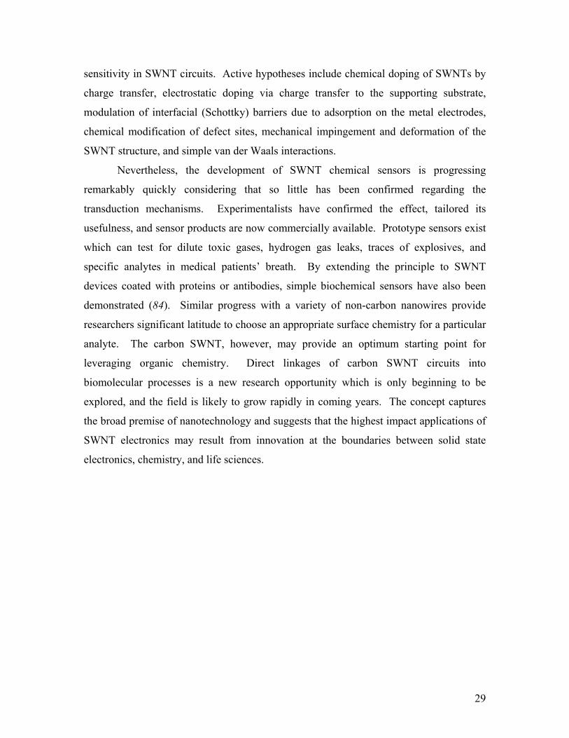
Figure 2. 1D quantization of the graphene bandstructure for different nanotube symmetries. The top row corresponds to an “armchair” nanotube in which a subband directly intersects the K symmetry points (a,b) and results in a metallic bandstructure (c). In the bottom row, a chrial nanotube’s subbands miss all of the K points (d,e) and the bandstructure is semiconducting. Reproduced from Dresselhaus et al. (85).
31
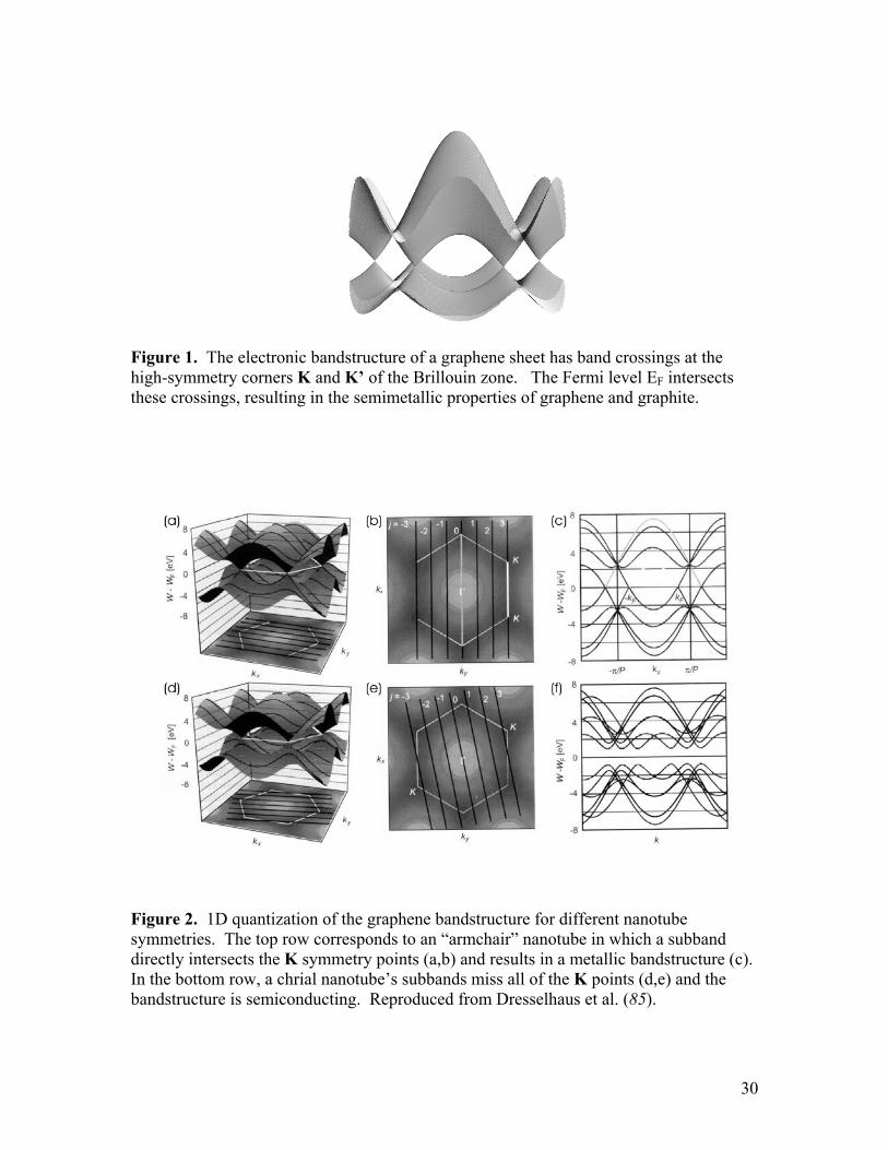
Figure 3. SWNT resistance versus device length. At very short lengths, a metallic SWNT is quasi-ballistic and the device resistance can approach the fundamental minimum of 6.5 kΩ. As device lengths exceed the mean free path for acoustic-phonon scattering, the resistance becomes diffusive with a resistivity of approximately 6 kΩ/µm. Reproduced from Li et al. (14)
32
Figure 4. SWNT current and resistance (inset) versus applied bias V. Over a wide bias range, the resistance increases linearly with V and is relatively insensitive to temperature. The behavior matches a model in which low-energy, acoustic phonon scattering is nearly absent and the resistance is predominantly due to high-energy, optical phonon emission. Note that this device, which is approximately 1 µm in length, has a small but non-negligible contact resistance. Reproduced from Yao et al. (16)
33
Figure 5. Differential conductance of a metallic SWNT 200nm in length. With sufficiently good contacts, the SWNT conductance approaches the theoretical limit of 4e2/h. The periodic oscillations with gate bias Vg correspond to Fabry-Perot interferences of electrons reflecting off the source and drain electrodes. This measurement is performed at T = 4K. From Wenjie et al. (22)
34
Figure 6. Gate dependence of an ambipolar SWNT FET. At positive gate bias, the conductance is primarily due to electron carriers, while at negative gate the carriers are holes. Near the threshold voltage, the Schottky barriers for holes and electrons are approximately equal and both carriers can be injected when the source-drain bias is large. Alternately, small biases maximize the achievable on-off ratio. From Y-M. Lin et al. (86).
35
Figure 7. Schottky barrier contacts limit the maximum possible drive current in a SWNT FET. The barrier height is sensitive to both the SWNT diameter and the contact metal. For low work function metals like Pd contacting small gap (large diameter) SWNTs, the effective barrier is minimized and maximum currents are achieved. The data points shown here are measured with a 0.5V source-drain bias at a gate voltage Vg – VT = -0.5V. From Chen et al. (28).
36
Figure 8. The apparent majority carrier in SWNT FETs changes from electrons in air to holes in vacuum, with a strong dependence on the presence of oxygen. This effect is due to a shift in the work function of the connective Au electrodes. In air, the work function mismatch to the SWNT results in a smaller Schottky barrier for holes than for electrons. In vacuum, the Au work function increases and the reverse becomes true. From Derycke et al. (39).
37
Figure 9. In traditional semiconductor devices, degenerately doped semiconductors form the source and drain contacts to the semiconducting channel. Similar effects in SWNT FETs can minimize Schottky barrier effects. Here, a partly-exposed SWNT is oxidized by SbCl6
- ions in order to degenerately dope the portions which contact the source and drain electrodes. The resulting FET characteristics exhibit a sharp conductance transition and very small subthreshold swing S, both of which may be attributed to switching by the SWNT body. From Chen et al. (24).
38
Figure 10. Electroluminescence from a long, single SWNT in a FET configuration. The electron-hole recombination length is short (~ 1 µm) compared to the length of the device, so the point of highest luminescence is easily resolved within the electrodes. Furthermore, this site can be controlled by varying the gate voltage Vg. This figure depicts the luminescence at four different values of Vg. From Freitag et al. (53).
39
Figure 11. Photoconductivity from an individual SWNT in a FET configuration. Incident radiation produces a large increase in conductivity if it is resonantly tuned to form electron-hole pairs (top). The effect is sensitive to both photon energy (bottom) and polarization (bottom, inset), with polarizations parallel to the SWNT generating the largest photocurrents. The primary resonance near 1.4 eV is due to the creation of excitons (the “E22
” transition), and the higher energy peak is a sideband attributed to exciton-phonon coupling. Adapted from Qiu et al. (87)
40
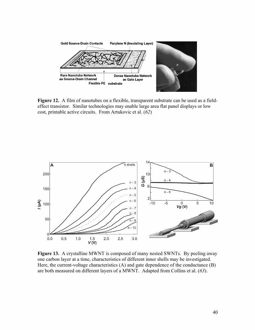
Figure 12. A film of nanotubes on a flexible, transparent substrate can be used as a field-effect transistor. Similar technologies may enable large area flat panel displays or low cost, printable active circuits. From Artukovic et al. (62)
Figure 13. A crystalline MWNT is composed of many nested SWNTs. By peeling away one carbon layer at a time, characteristics of different inner shells may be investigated. Here, the current-voltage characteristics (A) and gate dependence of the conductance (B) are both measured on different layers of a MWNT. Adapted from Collins et al. (63).
41
Figure 14. A SWNT cathode is a very effective field emitter, with turn-on fields as low as 1V/µm. The emitted electron beam can be used to light a phosphor or, as shown here, to generate X-rays medical imaging. Adapted from Yue et al (82).
Figure 15. The chemical sensitivity of SWNT FETs may be directed towards different analytes by coating or chemically functionalizing the devices in different ways. Using this approach, sensors selective to various gases and liquids have been demonstrated. Here, a starch-based polymer coating makes an n-type SWNT device sensitive to different concentrations of CO2 gas. The measurement at left is performed under fixed bias conditions (Vg = +6, VSD = 0.2V). Similar devices are under development for capnography, the monitoring of patient respiration, in which the desired dynamic range is the 0 to 10% CO2 range. Adapted from Star et al (88).
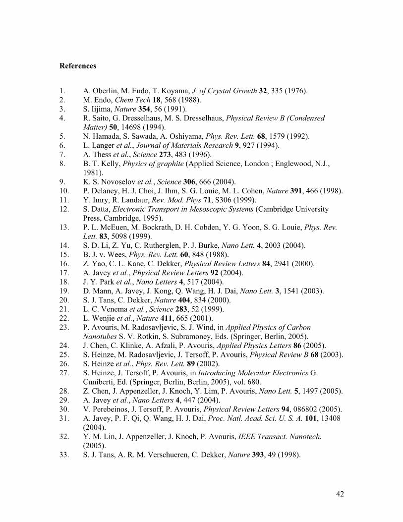
42
References
1. A. Oberlin, M. Endo, T. Koyama, J. of Crystal Growth 32, 335 (1976). 2. M. Endo, Chem Tech 18, 568 (1988). 3. S. Iijima, Nature 354, 56 (1991). 4. R. Saito, G. Dresselhaus, M. S. Dresselhaus, Physical Review B (Condensed
Matter) 50, 14698 (1994). 5. N. Hamada, S. Sawada, A. Oshiyama, Phys. Rev. Lett. 68, 1579 (1992). 6. L. Langer et al., Journal of Materials Research 9, 927 (1994). 7. A. Thess et al., Science 273, 483 (1996). 8. B. T. Kelly, Physics of graphite (Applied Science, London ; Englewood, N.J.,
1981). 9. K. S. Novoselov et al., Science 306, 666 (2004). 10. P. Delaney, H. J. Choi, J. Ihm, S. G. Louie, M. L. Cohen, Nature 391, 466 (1998). 11. Y. Imry, R. Landaur, Rev. Mod. Phys 71, S306 (1999). 12. S. Datta, Electronic Transport in Mesoscopic Systems (Cambridge University
Press, Cambridge, 1995). 13. P. L. McEuen, M. Bockrath, D. H. Cobden, Y. G. Yoon, S. G. Louie, Phys. Rev.
Lett. 83, 5098 (1999). 14. S. D. Li, Z. Yu, C. Rutherglen, P. J. Burke, Nano Lett. 4, 2003 (2004). 15. B. J. v. Wees, Phys. Rev. Lett. 60, 848 (1988). 16. Z. Yao, C. L. Kane, C. Dekker, Physical Review Letters 84, 2941 (2000). 17. A. Javey et al., Physical Review Letters 92 (2004). 18. J. Y. Park et al., Nano Letters 4, 517 (2004). 19. D. Mann, A. Javey, J. Kong, Q. Wang, H. J. Dai, Nano Lett. 3, 1541 (2003). 20. S. J. Tans, C. Dekker, Nature 404, 834 (2000). 21. L. C. Venema et al., Science 283, 52 (1999). 22. L. Wenjie et al., Nature 411, 665 (2001). 23. P. Avouris, M. Radosavljevic, S. J. Wind, in Applied Physics of Carbon
Nanotubes S. V. Rotkin, S. Subramoney, Eds. (Springer, Berlin, 2005). 24. J. Chen, C. Klinke, A. Afzali, P. Avouris, Applied Physics Letters 86 (2005). 25. S. Heinze, M. Radosavljevic, J. Tersoff, P. Avouris, Physical Review B 68 (2003). 26. S. Heinze et al., Phys. Rev. Lett. 89 (2002). 27. S. Heinze, J. Tersoff, P. Avouris, in Introducing Molecular Electronics G.
Cuniberti, Ed. (Springer, Berlin, Berlin, 2005), vol. 680. 28. Z. Chen, J. Appenzeller, J. Knoch, Y. Lim, P. Avouris, Nano Lett. 5, 1497 (2005). 29. A. Javey et al., Nano Letters 4, 447 (2004). 30. V. Perebeinos, J. Tersoff, P. Avouris, Physical Review Letters 94, 086802 (2005). 31. A. Javey, P. F. Qi, Q. Wang, H. J. Dai, Proc. Natl. Acad. Sci. U. S. A. 101, 13408
(2004). 32. Y. M. Lin, J. Appenzeller, J. Knoch, P. Avouris, IEEE Transact. Nanotech.
(2005). 33. S. J. Tans, A. R. M. Verschueren, C. Dekker, Nature 393, 49 (1998).
43
34. R. Martel, T. Schmidt, H. R. Shea, T. Hertel, P. Avouris, Appl. Phys. Lett. 73, 2447 (1998).
35. M. Bockrath et al., Phys. Rev. B 61, 10606 (2000). 36. P. G. Collins, K. Bradley, M. Ishigami, A. Zettl, Science 287, 1801 (2000). 37. K. Bradley et al., Phys. Rev. Lett. 85, 4361 (2000). 38. R. Martel et al., Phys. Rev. Lett. 87, art. no. (2001). 39. V. Derycke, R. Martel, J. Appenzeller, P. Avouris, Appl. Phys. Lett. 80, 2773
(2002). 40. J. Kong et al., Science 287, 622 (2000). 41. T. Ando, Journal of the Physical Society of Japan 66, 1066 (1997). 42. H. Sakai, H. Suzuura, T. Ando, Journal of the Physical Society of Japan 72, 1698
(2003). 43. C. D. Spataru, S. Ismail-Beigi, L. X. Benedict, S. G. Louie, Physical Review
Letters 92 (2004). 44. R. Egger, Physical Review Letters 83, 5547 (1999). 45. C. Kane, L. Balents, M. P. A. Fisher, Physical Review Letters 79, 5086 (1997). 46. M. Bockrath et al., Nature 397, 598 (1999). 47. H. W. C. Postma, M. de Jonge, Z. Yao, C. Dekker, Physical Review B 62, 10653
(2000). 48. H. Ishii et al., Nature 426, 540 (2003). 49. R. Loudon, Am. J. Phys. 27, 649 (1959). 50. V. Perebeinos, J. Tersoff, P. Avouris, Physical Review Letters 92, 257402 (2004). 51. F. Wang, G. Dukovic, L. E. Brus, T. F. Heinz, Science 308, 838 (2005). 52. J. A. Misewich et al., Science 300, 783 (2003). 53. M. Freitag et al., Phys. Rev. Lett. 93, 076803 (2004). 54. M. Freitag, Y. Martin, J. A. Misewich, R. Martel, P. Avouris, Nano Lett. 3, 1067
(2003). 55. T. W. Odom, H. Jin-Lin, P. Kim, C. M. Lieber, Nature 391, 62 (1998). 56. J. W. G. Wildoer, L. C. Venema, A. G. Rinzler, R. E. Smalley, C. Dekker, Nature
391, 59 (1998). 57. R. H. Baughman et al., Science 284, 1340 (1999). 58. K. H. An et al., Advanced Materials 13, 497 (2001). 59. E. S. Snow, J. P. Novak, P. M. Campbell, D. Park, Applied Physics Letters 82,
2145 (2003). 60. E. S. Snow et al., Journal of Vacuum Science & Technology B 22, 1990 (2004). 61. K. Bradley, J. C. P. Gabriel, G. Gruner, Nano Lett. 3, 1353 (2003). 62. E. Artukovic, M. Kaempgen, D. S. Hecht, S. Roth, G. Gruner, Nano Letters 5,
757 (2005). 63. P. C. Collins, M. S. Arnold, P. Avouris, Science 292, 706 (2001). 64. M. Kruger, I. Widmer, T. Nussbaumer, M. Buitelaa, C. Schonenberger, New
Journal of Physics 5 (2003). 65. A. Bachtold et al., Nature 397, 673 (1999). 66. A. Bachtold et al., Phys. Rev. Lett. 87, 6801 (2001). 67. P. G. Collins, P. Avouris, Appl. Phys. A-Mater. Sci. Process. 74, 329 (2002). 68. S. Frank, P. Poncharal, Z. L. Wang, W. A. de Heer, Science 280, 1744 (1998).
44
69. P. Poncharal, C. Berger, Y. Zi, Z. L. Wang, W. A. d. Heer, J. Phys. Chem. B 106, 12104 (2002).
70. T. W. Ebbesen et al., Nature 382, 54 (1996). 71. J. Cumings, W. Mickelson, A. Zettl, Solid State Commun. 126, 359 (2003). 72. S. Banerjee, T. Hemraj-Benny, S. S. Wong, Adv. Mater. 17, 17 (2005). 73. M. J. Biercuk et al., Appl. Phys. Lett. 80, 2767 (2002). 74. R. H. Baughman, A. A. Zakhidov, W. A. d. Heer, Science 297, 787 (2002). 75. C. S. Du, J. Yeh, N. Pan, Nanotechnology 16, 350 (2005). 76. G. T. Wu et al., J. Electrochem. Soc. 146, 1696 (1999). 77. P. Kim, C. M. Lieber, Science 286, 2148 (1999). 78. M. M. J. Treacy, T. W. Ebbesen, J. M. Gibson, Nature 381, 678 (1996). 79. P. Poncharal, Z. L. Wang, D. Ugarte, W. A. de Heer, Science 283, 1513 (1999). 80. T. Rueckes et al., Science 289, 94 (2000). 81. J. M. Bonard, H. Kind, T. Stockli, L. A. Nilsson, Solid-State Electron. 45, 893
(2001). 82. G. Z. Yue et al., App. Phys. Lett. 81, 355 (2002). 83. G. U. Sumanasekera, C. K. W. Adu, S. Fang, P. C. Eklund, Phys. Rev. Lett. 85,
1096 (2000). 84. A. Star, J. C. P. Gabriel, K. Bradley, G. Gruner, Nano Lett. 3, 459 (2003). 85. M. S. Dresselhaus, P. Avouris, in Carbon Nanotubes M. S. Dresselhaus, P.
Avouris, Eds. (Springer-Verlag Berlin, Berlin, 2001), vol. 80, pp. 1-9. 86. Y.-M. Lin, P. Avouris, Electron Device Lett., in press (2005). 87. X. H. Qiu, M. Freitag, V. Perebeinos, P. Avouris, Nano Lett. 5, 749 (2005). 88. A. Star, T. R. Han, V. Joshi, J. C. P. Gabriel, G. Gruner, Advanced Materials 16,
2049 (2004).