Embed Size (px)
Citation preview

4206 J. Electrochem. Soc., Vol. 145, No. 12, December 1998 The Electrochemical Society, Inc.
Manuscript submitted September 2, 1997; revised man-uscript received June 29, 1998.
NTT System Electronics Laboratories assisted in meet-ing the publication costs of this article.
REFERENCES1. D. Hisamoto, K. Nakamura, M. Saito, N. Kobayashi, S.
Kimura, R. Nagai, T. Nishida, and E. Takeda, in Techn.Dig. mt. Electron Devices Meet,, IEEE, p. 829 (1992).
2. Y. Nakamura, N. Kobayashi, D. Hisamoto, K. Umeda,and R. Nagai, Jpn. J. Appl. Phys., 35, 1082 (1996).
3. T. Tsutsumi, H. Kotani, J. Komori, and S. Nagao, IEEETrans. Electron Devices, ED-37, 569 (1990).
4. M. Sekine, N. Itoh, T. Akimoto, T. Shinmura, D. T. C.Huo, Y. Kakuhara, K. Kajiyama, Y. Yamada, K.Yamazaki, and Y. Murao, p. 184, in Solid State De-vices and Materials, Extended Abstracts of JapanSociety of Applied Physics, Tsukuba, Japan (1992).
5. K. Sakuma, K. Machida, K. Kamoshida, Y. Sato, K. Imai,and E. Arai, J. Vac. Sci. Technol., B, 13, 902 (1995).
6. M. Miyake, S. Aoyama, S. Hirota, and T. Kobayashi, J.Electrochem. Soc., 135, 2872 (1988).
7. V. Kusumoto, K. Takakuwa, H. Hashinokuchi, T. Ikuta,and I. Nakayama, in Tungsten and Other RefractoryMetals for VLSI Applications III, V. A. Wells, Editor,p. 217, Materials Research Society, Pittsburgh, PA(1987).
8. I. M. Band, Vu. I. Kharitonor, and M. B. Trzhaskovskaya,At. Data Nucl. Data Tables, 23, 443 (1979).
9. H. F. Winters and J. W. Coburn, Surf. Sci. Rep., 14, 161(1992).
10. H. Ibach, in Electron Spectroscopy for Surface Analy-sis, H. Ibach, Editor, p. 1, Springer, Berlin (1977).
11. M. P. Seah and W. A. Dench, Surf. Interface Anal., 1, 2(1979).
12. M. L. Vu and B. N. Eldridge, J. Vac. Sci. Technol., A, 7,625 (1989).
13. T. Takahagi, Oyo Butsuri, 59, 1441 (1990).14. M. Ikeda, T. Rusyanto, and N. Nagashima, Hyomen
Kagaku, 15, 164 (1994).15. T. Ohno, V. Kado, M. Harada, and T. Tsuchiya, IEEE
Trans. Electron Devices, ED-42, 1481 (1995).16. V. Sato, T. Tsuchiya, T. Kosugi, and H. Ishii, in Pro-
ceedings of the 1995 IEEE International Silicon-on-Insulator Conference, p. 28, Tucson, AZ, IEEE (1995).
Thin-Film Properties and Barrier Effectiveness of Chemically
Vapor Deposited Amorphous WSi,, FilmM. 1. Wang, Y. C. un, J. Y. Lee, C. C. Wang, and M. C. Chen*
Department of Electronics Engineering, National Chiao-Tung University, Hsinchu, Taiwan
ABSTRACT
Thin-Film properties and barrier effectiveness against copper (Cu) diffusion of a thin amorphous WSi, layer wereinvestigated. The amorphous WSi layer was deposited by the chemical vapor deposition (CVD) method using the SiH4/WF6chemistry with the activation energy determined to be 3.0 kcal/mol. The CVD-WSi, film has a low film stress, low electri-cal resistivity, and excellent step coverage. The resistivity of the amorphous CVD-WSi layer increases with the depositiontemperature, but the residual stress of the layer decreases with the deposition temperature. The WSi/Si structure is ther-mally stable up to at least 600°C, while the copper-contacted Cu/WSijSi structure with a 50 nm thick WSi barrier is sta-ble only up to 550°C. Moreover, the Cu/WSijp -n junction diodes can sustain a 30 mm thermal annealing up to 500°C with-out causing degradation in electrical characteristics. Barrier failure of the WSi layer in the Cu/WSir/Si structure attemperatures above 550°C is attributed to Cu atoms diffusion via fast paths in the WSi layer. These fast paths were pre-sumably developed from grain growth of the WSi layer and/or thermal-stress-induced weak points in the WSi layer.
IntroductionAs the interconnect linewidth shrinks continuously to
deep-submicron dimensions, Alt metallurgy becomes inade-quate owing to its poor electromigration resistance; in ad-dition, the resistivity of Al alloys is higher than desired forfast integrated circuits (ICs). Therefore, other metals withlower resistivity and superior electromigration resistancehave been extensively studied.1-3 Copper (Cu) has a lowerresistivity than aluminum (Al) and it has an excellent elec-tromigration resistance. Moreover, Cu can be deposited bychemical vapor deposition (CVD).4 However, Cu diffusesfast in Si substrate and forms Cu—Si compounds at lowtemperatures (about 200°C),7'8 causing deep-level traps inSi. Moreover, Cu adheres poorly to dielectric layers anddrifts through oxide under field acceleration.9"° Therefore,a diffusion barrier between Cu and its surrounding layers isconsidered a prerequisite for Cu to be useful in siliconbased IC applications.
Although many studies have shown that the sputter-deposited amorphous materials are very effective barriersfor Cu metallization due to the absence of gram bound-aries,113 it is difficult to deposit metal barriers with accept-able conformity in submicron contact holes using the sput-ter deposition method. In contrast, CVD generally offers amuch better conformal deposition than the physical vapordeposition (PVD) method; therefore, there is increasing in-
* Electrochemical Society Active Member.
terest in depositing amorphous barriers by CVD. Chemical-ly vapor deposited silicon-rich (Si/W atomic ratio largerthan 2.0) WSi layers used in polycide application has beenextensively investigated using either SiH4/WF6 '-z orSiH2C12/WF6 chemistry.22-25 However; no study has beenmade on metal-rich (Si/W atomic ratio less than 2.0) WSilayers with respect to their barrier effectiveness against Cudiffusion.
In this study, film properties and barrier effectiveness ofthin, amorphous, metal-rich WSi layers were investigatedusing electrical measurement as well as material analysis.The amorphous WSi layers were deposited by low-pres-sure chemical vapor deposition (LPCVD) using SiH4 re-duction of WF,. We evaluated the barrier capability of theamorphous WSi layers for Cu metallization using a struc-ture of Cu/WSir/p-n junction diodes. Stability of the un-patterned samples of Cu/Si, WSi,/Si, and Cu/WSiJSistructures was also investigated. The electrical measure-ment is believed to be a much more sensitive technique forbarrier-failure detection than the material analyses, whilethe material analyses can provide microscopic informationof material change, which is helpful to the understandingof failure mechanisms of the barrier layers. The results ofthis study may be useful for the integration of the amor-phous WSi in Cu metallization applications.
ExperimentalThe thermal stability of barrier layers was evaluated by
measuring leakage current of thermally annealed Cu/bar-
) unless CC License in place (see abstract). ecsdl.org/site/terms_use address. Redistribution subject to ECS terms of use (see 140.113.38.11Downloaded on 2014-04-28 to IP
J. Electrochem. Soc., Vol. 145, No. 12, December 1998 @ The Electrochemical Society, Inc.
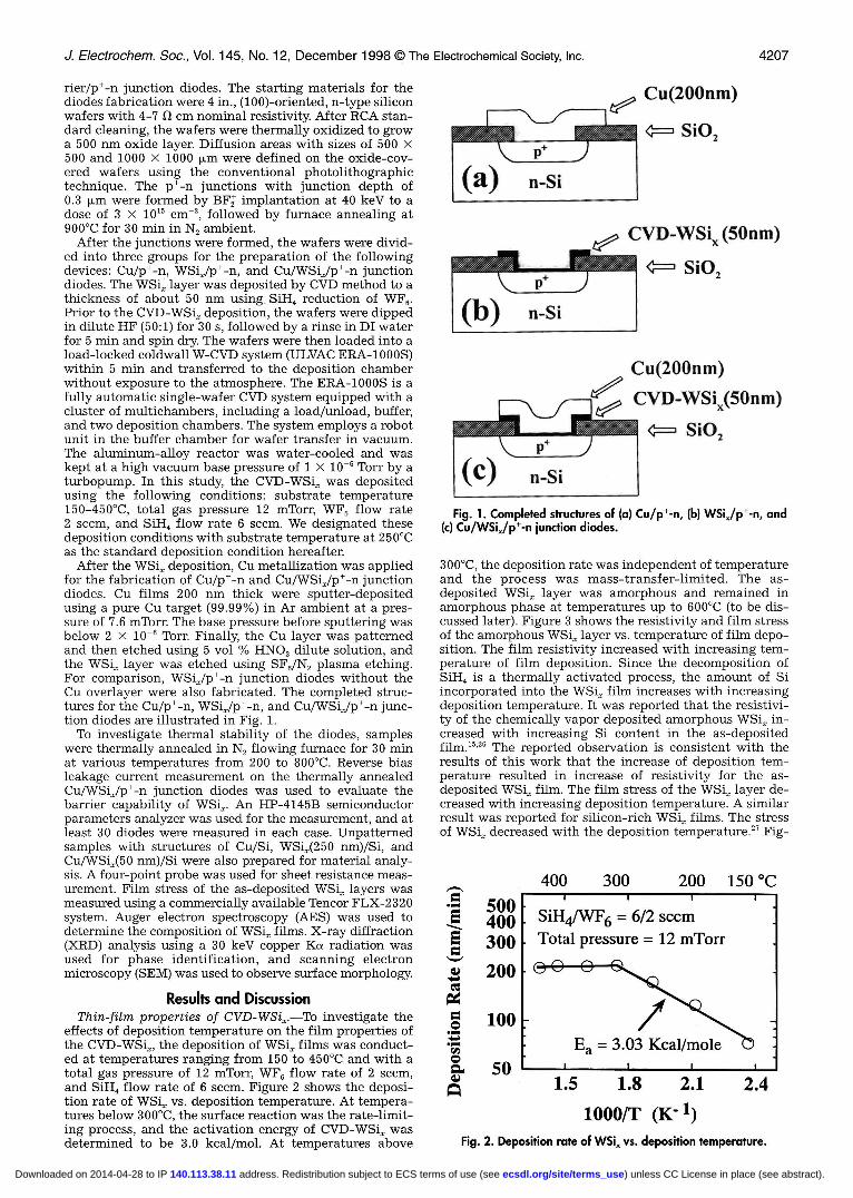
rier/pc-n junction diodes. The starting materials for the diodes fabrication were 4 in., (100)-oriented, n-type silicon wafers with 4-7 R cm nominal resistivity. After RCA stan- dard cleaning, the wafers were thermally oxidized to grow a 500 nm oxide layer. Diffusion areas with sizes of 500 X 500 and 1000 X 1000 pm were defined on the oxide-cov- ered wafers using the conventional photolithographic technique. The p+-n junctions with junction depth of 0.3 pm were formed by BF: implantation at 40 keV to a dose of 3 X 10¹⁵ em-', followed by furnace annealing at 900°C for 30 min in N, ambient.
After the junctions were formed, the wafers were divid- ed into three groups for the preparation of the following devices: Cu/p+-n, WSi Jp+-n, and Cu/WSi,/p+-n junction diodes. The WSi, layer was deposited by CVD method to a thickness of about 50 nm using. SiH, reduction of WF,. Prior to the CVD-WSi, deposition, the wafers were dipped in dilute HF (50:l) for 30 s, followed by a rinse in DI water for 5 min and spin dry. The wafers were then loaded into a load-locked coldwall W-CVD system (ULVAC ERA-1000s) within 5 min and transferred to the deposition chamber without exposure to the atmosphere. The ERA-1000s is a fully automatic single-wafer CVD system equipped with a cluster of multichambers, including a load/unload, buffer, and two deposition chambers. The system employs a robot unit in the buffer chamber for wafer transfer in vacuum. The aluminum-alloy reactor was water-cooled and was kept at a high vacuum base pressure of 1 X Torr by a turbopump. In this study, the CVD-WSi, was deposited using the following conditions: substrate temperature 150-45O0C, total gas pressure 12 mTorr, WF, flow rate 2 sccm, and SiH, flow rate 6 sccm. We designated these deposition conditions with substrate temperature at 250°C as the standard deposition condition hereafter.
After the WSi, deposition, Cu metallization was applied for the fabrication of Cu/p+-n and Cu/WSi,/p+-n junction diodes. Cu films 200 nm thick were sputter-deposited using a pure Cu target (99.99%) in Ar ambient at a pres- sure of 7.6 mTom The base pressure before sputtering was below 2 X lo-, Tom. Finally, the Cu layer was patterned and then etched using 5 vol % HNO, dilute solution, and the WSi, layer was etched using SF6/N, plasma etching. For comparison, WSiJp+-n junction diodes without the Cu overlayer were also fabricated. The completed struc- tures for the Cu/p+-n, WSi,/p+-n, and Cu/WSi,/p+-n junc- tion diodes are illustrated in Fig. 1.
To investigate thermal stability of the diodes, samples were thermally annealed in N, flowing furnace for 30 min at various temperatures from 200 to 800°C. Reverse bias leakage current measurement on the thermally annealed Cu/WSiJp+-n junction diodes was used to evaluate the barrier capability of WSi,. An HP-4145B semiconductor parameters analyzer was used for the measurement, and at least 30 diodes were measured in each case. Unpatterned samples with structures of Cu/Si, WSiJ250 nm)/Si, and Cu/WSi,(50 nm)/Si were also prepared for material analy- sis. A four-point probe was used for sheet resistance meas- urement. Film stress of the as-deposited WSi, layers was measured using a commercially available Tencor FLX-2320 system. Auger electron spectroscopy (AES) was used to determine the composition of WSi, films. X-ray diffraction (XRD) analysis using a 30 keV copper Ka radiation was used for phase identification, and scanning electron microscopy (SEM) was used to observe surface morphology.
Results and Discussion Thin-film properties of CVD-WSi,.-To investigate the
effects of deposition temperature on the film properties of the CVD-WSi,, the deposition of WSi, films was conduct- ed at temperatures ranging from 150 to 450°C and with a total gas pressure of 12 mTorr, WF, flow rate of 2 sccm, and SiH, flow rate of 6 sccm. Figure 2 shows the deposi- tion rate of WSi, vs. deposition temperature. At tempera- tures below 300°C, the surface reaction was the rate-limit- ing process, and the activation energy of CVD-WSi, was determined to be 3.0 kcal/mol. At temperatures above
LJLJ / (a) n-si
C===, SiO,
/ (b) n-si
Fig. 1. Completed structures of (a) Cu/p+-n, (b) WSi,/p+-n, and (c) Cu/WSi,/p+-n junction diodes.
30OoC, the deposition rate was independent of temperature and the process was mass-transfer-limited. The as- deposited WSi, layer was amorphous and remained in amorphous phase at temperatures up to 600°C (to be dis- cussed later). Figure 3 shows the resistivity and film stress of the amorphous WSi, layer vs. temperature of film depo- sition. The film resistivity increased with increasing tem- perature of film deposition. Since the decomposition of SiH, is a thermally activated process, the amount of Si incorporated into the WSi, film increases with increasing deposition temperature. It was reported that the resistivi- ty of the chemically vapor deposited amorphous W S i in- creased with increasing Si content in the as-deposited film.15s26 The reported observation is consistent with the results of this work that the increase of deposition tem- perature resulted in increase of resistivity for the as- deposited WSi, film. The film stress of the WSi, layer de- creased with increasing deposition temperature. A similar result was reported for silicon-rich WSi, films. The stress of WSi, decreased with the deposition temperature.'' Fig-
- E
SiHd/WF6 = 612 sccm
E
10OOlT (K- l) Fig. 2. Deposition rate of WSi, vs. deposition temperature.
) unless CC License in place (see abstract). ecsdl.org/site/terms_use address. Redistribution subject to ECS terms of use (see 140.113.38.11Downloaded on 2014-04-28 to IP

4208 J. Electrochem. Soc., Vol. 145, No. 12, December 1998 The Electrochemical Society, Inc.
300 , 1000
800-&-Stress - - I
__ IResistivity a
180 ' ' ' ' 0 '-200 250 300 350 400 450
Temperature (°C)Fig.3. Film resistivity and stress of WSi vs. deposition temperature.
ure 4 shows the WSi films deposited on submicron trench-es with aspect ratios of 2 and 5 using the "standard depo-sition condition." A highly conformal deposition of CVD-WSi was obtained.
Electrical measurement .—T he Cu/pt-n, Cu/WSijp-n,and WSijp-n junction diodes were thermally annealed inan N2 flowing furnace for 30 mm at various temperatures.Figure 5 shows the statistical distributions of reverse biasleakage current density measured at —5 V for the Cu/pt-n,
Fig. 4. Step coverage of WSi films deposited on submicrontrenches with aspect ratio of (a) 2.0 and (b) 5.0. The WSi filmswere deposited at a total gas pressure of 12 mlbrr, WF6 How rateof 2 sccm, SiH4 flow rate of 6 sccm, and substrate temperature of250°C.
Cu/WSi/p-n, and WSijp-n junction diodes in which theWSjr barrier layers were deposited using our standard dep-osition conditions. The Cu/p-n diodes without any barrierlayer between Cu and Si substrate failed after annealing at200°C (Fig. 5a). With a barrier layer of 50 nm CVD-WSibetween Cu and Si substrate, the Cu/WSijp-n junctiondiodes were able to retain the devices integrity up to 500°C.After annealing at 550°C, however, the diodes completelyfailed (Fig. 5b). For comparison, WSi/p-n junction diodeswithout a Cu overlayer were also investigated. TheWSi/p-n junction diodes retained their integrity up to700°C and revealed only slight degradation after annealingat 750°C (Fig. 5c), presumably due to WSi2 formation(which consumed the substrate Si) and its grain growth aswell as increase of film stress for the thermally annealedWSiX layer. Clearly, the WSi layer itself did not degradethe electrical characteristics of the WSi/p-n junctiondiodes up to 700°C, and the complete failure of theCu/WSi/p-n junction diodes at 550°C (Fig. Sb) is attrib-uted to the presence of Cu overlayer on the WSi. surface.
Material analyses .—XRD analysis.—Figure 6 showsXRD spectra for the Cu/Si and WSi(250 nm)/Si samplesafter annealing at various temperatures. For the sample ofCu/Si annealed at 150°C, the XRD spectrum remainedunchanged as compared with the as-deposited sample (notshown). However, a strong Cu3Si peak appeared for thesample annealed at 200°C, indicating formation of coppersiicide. After annealing at 250°C, the (200) peak of Cu dis-appeared, indicating that the Cu overlayer might havetranslated into Cu3Si completely (Fig. 6a). For the sampleof WSi/250 nm)/Si, the amorphous state of the as-deposit-ed WSi remained unchanged even after annealing at600°C. With annealing temperature raised to 650°C, a num-ber of peaks belonging to WSi2 phase appeared, indicatingsilicidation of the WSi,, layer (Fig. 6b).
The XRD spectra for the Cu/WSir(50 nm)/Si multilayerstructure are illustrated in Fig. 7. Presumably because theWSi layer was too thin and was covered with a 200 nmthick Cu film, the amorphous band belonging to the WSilayer was too weak to be observed. The crystallizationtemperature of the WSi layer in the Cu/IWSiJSi structure
Leakage Current Density (A/cm2)Fig. 5. Histograms showing distributions of reverse bias leakage
current density for (a) Cu/p-n, (b) Cu/WSi,/p-n, and (c)WSi/p-n junction diodes annealed at various temperatures.
I270
, 240
• 210
-;-(a)!
Ctp°. CuIWSi(5Onm)/p-n WSi,,(SOnm)/p°-n
-. _
Ito4t..Ilo.,Io'10410..'I-3
) unless CC License in place (see abstract). ecsdl.org/site/terms_use address. Redistribution subject to ECS terms of use (see 140.113.38.11Downloaded on 2014-04-28 to IP

J. Electrochem. Soc., Vol. 145, No. 12, December 1998 The Electrochemical Society, Inc. 4209
was found to be around 600°C. By comparing XRD spectraof the Cu/WSiJSi sample with that of the WSiJSi sampleshown in Fig. 6b, we found that the crystallization tem-perature of WSi layer in the Cu/WSiJSi structure isabout 50°C lower than that in the WSiJSi sample. Thisdiscrepancy is presumably due to the presence of Cu over-layer for the Cu/WSiJSi sample. It was reported that thecrystallization temperature of amorphous Ta36Si14N50 de-posited on sapphire dropped from 1100 to 900°C when theTa36Si14N50 film was in contact with a polycrystalline cop-per layer.z8 In this study we found that the WSr/Si struc-ture remained stable up to 600°C with no silicide phaseformation (Fig. 6b); however, silicide phase appeared forthe Cu/WSiJSi sample annealed at 600°C due to the pres-ence of Cu layer in contact with WSi (Fig. 7).
The fact that the presence of Cu overlayer in theCu/WSiJSi sample reduced the crystallization tempera-ture of WSi. may presumably be explained as follows.
I
20 25 30 35 40 45 50 55 60
2 0 (DEGREE)Fig. 7. XRD spectra for Cu/WSi,,/Si samples annealed at various
temperatures.
First, a small amount of Cu atom penetrated the WSi,layer to form Cu3Si phase at the WSiJSi interface duringthermal annealing at 600°C. This penetration probablyoccurred via localized defects, such as vacancy-accumu-lated voids, thermal-stress-induced inicrocracks of theWSr layer; and/or grain boundaries which developed fromgrain growth of the WSi layer. Second, the Cu3Si forma-tion at the WSlr/S interface generated point defects, e.g.,Si self-interstitial or vacancy in the Si lattice,29'3° promot-
___________________________________________ing silicidation of WSr at the WSiJSi interface. Anotherpossible mechanism for the accelerated silicidation of theWSi can be the introduction of nucleation sites by thepenetrated Cu atoms. The formation of copper silicide andtungsten silicide at the WSiJSi interface resulted in a netvolume change and produced more fast paths for Cu diffu-sion, thus further degrading the WSi,, barrier capability.Table I summarizes the formation of silicides on thermal-ly annealed Cu and/or WSi contacted structures.Sheet resistance measurement .—T he sheet resistancechange of annealed samples, normalized to the as-deposit-ed sheet resistance value, is denoted as LRs/Rs % anddefined as follows
ARs = RSafternnea1—
RSa_depoited x 100%Rs RS=_deposited
Figure 8 shows the percentage change of sheet resistancevs. annealing temperature for the Cu/Si and WSiJSi sam-ples. The sheet resistance of Cu/Si remained constant fol-lowing anneal at temperatures up to 175°C but increaseddrastically after annealing at 200°C. The drastic increasein sheet resistance is attributed to the formation of high-
Table I. Suicide formation on various Cu and WSu,— contacted structures.
20 25 30 35 40 45 50 55 60
20 (DEGREE)Fig. 6. XRD spectra for (a) Cu/Si and (b) WSi,/Si samples
annealed at various temperatures.
Annealing temperature(°C)
Contact structureCu/Si WSi/Si Cu/WSiISi
200 Cu3Si X x500 Cu3Si X X600 X W55i3, WSi2, Cu3Si650 WSi2 WSi2, Cu3Si
C 0
650 t
.
—
.—
(a)
20 25 30 35 40 45 50 55 60
2 0 (DEGREE)
(b)
.—C. t C —. —.
JJULJU&Lamorphous WSi
amorphous WSi
Note: "X" indicates no observation of suicide phase.
) unless CC License in place (see abstract). ecsdl.org/site/terms_use address. Redistribution subject to ECS terms of use (see 140.113.38.11Downloaded on 2014-04-28 to IP

4210 J. Electrochem. Soc., Vol. 145, No. 12, December 1998 The Electrochemical Society, Inc.
1600
1200
800
400
00 200 400 600 800
Figure 9 shows the percentage change of sheet resistancevs. annealing temperature for the Cu/WSiJSi samples inwhich the WSi layers were deposited at different temper-atures. It can be seen that the change of sheet resistance isnot sensitive to the deposition temperature of the WSilayer. The sheet resistance of the Cu/WSiJSi samples de-creased slightly after annealing at 400°C, presumably dueto out-diffusion of impurities, grain growth of the Culayer, and the annealing out of sputter-induced damage inthe Cu film. Thermal stability of the Cu/WSir/Si multilay-er structure reached 550°C. After annealing at 600°C, dras-tic increase in sheet resistance was found for all samples,implying failure of the Cu/WSiJSi structure. This is con-sistent with the results of XRD analysis shown in Fig. 7.
Temperature (°C)Fig. 8. Percentage change of sheet resistance vs. annealing tem-
perature for the samples of Cu/Si and WSi,/Si.
resistivity 1"-Cu3Si precipitate, as confirmed by XRDanalysis shown in Fig. 6a. For the WSiJSi sample, thesheet resistance remained stable up to 600°C. With thesample annealed at temperatures above 650°C, the sheetresistance decreased slightly with increasing annealingtemperature. This is attributed to the formation of low-resistivity WSi2 phase at temperatures above 650°C, asshown in Fig. 6b.
2000
1500
1000
500
0
-.5000 200 400 600 800
Temperature (°C)Fig. 9. Percentage change of sheet resistance vs. annealing tem-
perature for the Cu/WSi/Si samples with the WSi films depositedat different substvate temperatures.
Deposition temperatures:----250°C—R-- 300°C---O--350°C
As-deposited
I • I •
— -__?ØB 20.0kV 20.éK 9en.
Fig. 10. Oblique view SEM micrographs for the WSik/Si samples(a) as-deposited and thermally annealed at (b) 600, (c) 650, and(d) 800°C.
Fig. 11. SEM micrographs for the Cu/WSi/p-n junction diodes(a) os-deposited and thermally annealed at (b) 500 and (ci 550°C.
) unless CC License in place (see abstract). ecsdl.org/site/terms_use address. Redistribution subject to ECS terms of use (see 140.113.38.11Downloaded on 2014-04-28 to IP

J. Electrochem. Soc., Vol. 145, No. 12, December 1998 The Electrochemical Society, Inc. 4211
Table II. Comparative results of barrier effectiveness for WSi,, determined by different techniques of measurement and/or analysis.
SEM observation.—Figure 10 shows the SEM micrographsfor the WSi(250 nm)/Si samples before and after thermalannealing. No grain-like structure was observed for boththe as-deposited as well as the 600°C-annealed samples(Fig. 10a and b). Grain-like structure was observed for theWSi film annealed at 650°C, and it became more obviousat 800°C (Fig. lOc and d). This is consistent with the resultsof XRD analysis (Fig. 6b) and sheet resistance measure-ment (Fig. 8). Figure 11 shows the SEM micrographs forthe Cu/WSi(50 nm)/pF_n junction diodes before and afterthermal anneal. The integrity of the Cu/barrier/Si struc-ture basically remained unchanged after annealing at500°C (Fig. llb); however, large Cu3Si precipitates werefound after annealing at 550°C. With cross-sectional SEManalysis, it has been determined that a fully developedCu3Si precipitate is inverted pyramid-shaped and bound-ed by Si{lll} planes (Fig. llc).29 Comparative results ofbarrier effectiveness for the WSi layers determined bydifferent techniques of measurement and/or analysis aresummarized in Table II.
ConclusionsThin-film properties of amorphous WSi layers and ther-
mal stability of Cu/WSi/p-n junction diodes were investi-gated. The amorphous WSi layer was deposited by (CVD)method using the SiH4/WF6 chemistry with the activationenergy determined to be 3.0 kcal/mol. The WSi film has alow film stress, low electrical resistivity, and excellent stepcoverage. The WSi/Si structure is thermally stable up to atleast 600°C, while the copper-contacted Cu/WSi1/Si struc-ture with a 50 nm thick WSi barrier is stable only up to550°C. Moreover, the Cu/WSiJp-n junction diodes are ableto sustain a 30 mm thermal annealing at temperatures up to5 00°C without causing degradation to the devices electricalcharacteristics. Barrier failure of the WSiX layer at temper-atures above 550°C is attributed to Cu diffusion via fastpaths, which are presumably developed from grain growthof the WSi layer and/or thermal stress-induced weakpoints in the WSi layer.
AcknowledgmentsThis work was supported by the National Science Coun-
dll (ROC) under contract no. NSC86-2215-E-009-040.
Manuscript submitted September 12, 1997; revised man-uscript received August 21, 1998.
National Chiao-Tung University assisted in meeting thepublication costs of this article.
REFERENCES1. 5. P Murarka, R. J. Gutmann, A. E. Kaloyeros, and
W. A. Lanford, Thin Solid Films, 230, 257 (1993).2. B. Roberts, A. Harms, and R. L. Jackson, Solid State
Technol., 69 (Feb 1995).3. J. M. E. Harper, E. G. Colgan, C. K. Hu, J. P. Hummel,
L. P Buchwalter, and C. E. Uzoh, MRS Bull., 23(Aug 1994).
4. V M. Dubin and Y. S. Diamand, J. Electrochem. Soc.,144, 898 (1997).
5. D. H. Kim, R. H. Wentorf, and W. N. Gill, J. Elec-trochem. Soc., 140, 3273 (1993).
6. J. C. Chiou, K. C. Juang, and M. C. Chen, .1. Electro-chem. Soc., 142, 177 (1995).
7. C. A. Chang, 31 Appl. Phys., 67, 566 (1990).8. L. Stolt and F M D'Heurle, Thin Solid Films, 189, 269
(1990).9. Y. S. Diamand, A. Dedhia, D. Hoffstetter, and W. G.
Oldham, J. Electrochem. Soc., 140, 2427 (1993).10. A. L. S. Loke, C. Ryu, C. P Yue, J. S. H. Cho, and S. S.
Wong, IEEE Electron Device Lett., EDL-17, 549(1996).
11. M. A. Nicolet, Thin Solid Films, 107, 415 (1978).12. R. S. Nowicki and M.-A. Nicolet, Thin Solid Films, 96,
317 (1982).13. J. S. Reid, R. Y. Liu, P M. Smith, R. P Ruiz, and M.-A.
Nicolet, Thin Solid Films, 262, 218 (1995).14. D. L. Brors, J. A. Fair, K. A. Monnig, and K. C. Sara-
swat, Solid State Technol., 183 (Aprll 1983).15. T. E. Clark, J. Vac. Sci. Technol., B6, 1678 (1988).16. M. Kottke, F Pintchovski, T. R. White, and P 3. Tobin,
31 Appl. Phys., 60, 2835 (1986).17. Y. Shioya, T. Itoh, I. Kobayashi, and M. Maeda, dl Elec-
trochem. Soc., 133, 1475 (1986).18. Y. Shioya and M. Maeda, J. Appl. Phys., 60, 327 (1986).19. D. K. Sadana, A. B. Morgan, M. H. Norcott, and S.
Naik, J. Appl. Phys., 62, 2830 (1987).20. D. Dobkin, L. Bartholomew, G. McDaniel, and J. De-
Dontney, J. Elect rochem. Soc., 137, 1623 (1990).21. N. Thomas, A. M. Dutron, C. Vahlas, C. Bernard, and R.
Madar, 3. Electrochem. Soc., 142, 1608 (1995).22. T. H. Wu, R. S. Roster, B. C. Lamartine, R. B. Gregory,
and H. G. Tompkins, 3. Vac. Sci. Technol., B6, 1707(1988).
23. 5. G. Telford, M. Eizenberg, M. Chang, A. K. Sinha,and P R. Gow, Appl. Phys. Lett., 62, 1766 (1993).
24. T. Hara, T. Miyamoto, and T. Yokoyama, 3. Elec-trochem. Soc., 136, 1177 (1989).
25. J. E. J. Schmitz, Chemical Vapor Deposition of Tung-sten and Tungsten Silicides for VLSI! ULSI Applica-tions, pp. 171—208, Noyes Publications, Park Ridge,NJ (1992).
26. J. H. Sone and H. J. Kim, in Advanced Metallizationand Processing for Semiconductor Devices and Cir-cuits, A. Katz, S. P. Murarka, Y. I. Nissim, andJ. M. E. Harper, Editors, Vol. 260, p. 621, MaterialsResearch Society, Pittsburgh, PA (1990).
27. Y. Shioya, T. Itoh, S. Inoue, and M. Maeda, 3. AppI.Phys., 58, 4194 (1985).
28. B. Kolawa, J. S. Chen, 3. 5. Reid, P J. Pokela, and M. A.Nicolet, J. Appl. Phys., 70, 1369 (1991).
29. K. Holloway, P M. Fryer, C. Cabral, Jr., 3. M. F. Harp-er, P 3. Bailey, and K. H. Kelleher, 3. Appl. Phys., 71,5433 (1992).
30. M. Ronay and R. G. Schad, Phys. Rev. Lett., 64, 2042(1990).
Measurement/analysis methods
Leakage cunentmeasurement Materials analysisThermal stability Sheet resistance
Diode structuretemperature
(°C)Layeredstructure
measurement(°C)
XRD(°C)
SEM(°C)
Cu/p-nCu/WSi/pt-nWSi/p-n
150500700
Cu/SiCu/W5i/Si
WSiJSi
175550650
150550600
175500600
) unless CC License in place (see abstract). ecsdl.org/site/terms_use address. Redistribution subject to ECS terms of use (see 140.113.38.11Downloaded on 2014-04-28 to IP