Embed Size (px)
Citation preview
1
TI在线培训:智能穿戴设备设计要点与难点
4/25/2017
1
培训课题
• 智能穿戴设备概要
• 多主多从在智能穿戴设备的应用衍生
• 穿戴设备低功耗设计要点
• 小体积、低功耗电源解决方案
• 心率测量模拟前端方案
2
2
可穿戴设备场景及蓝牙5.0应用
3
Michael Qian
无线连接现场应用工程师
4
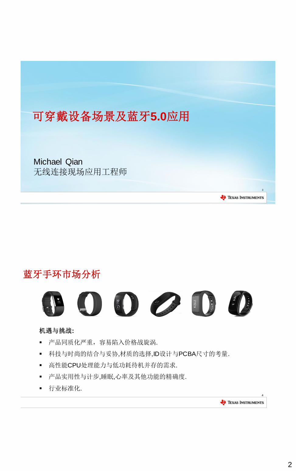
蓝牙手环市场分析
机遇与挑战:
产品同质化严重,容易陷入价格战旋涡.
科技与时尚的结合与妥协,材质的选择,ID设计与PCBA尺寸的考量.
高性能CPU处理能力与低功耗待机并存的需求.
产品实用性与计步,睡眠,心率及其他功能的精确度.
行业标准化.
3
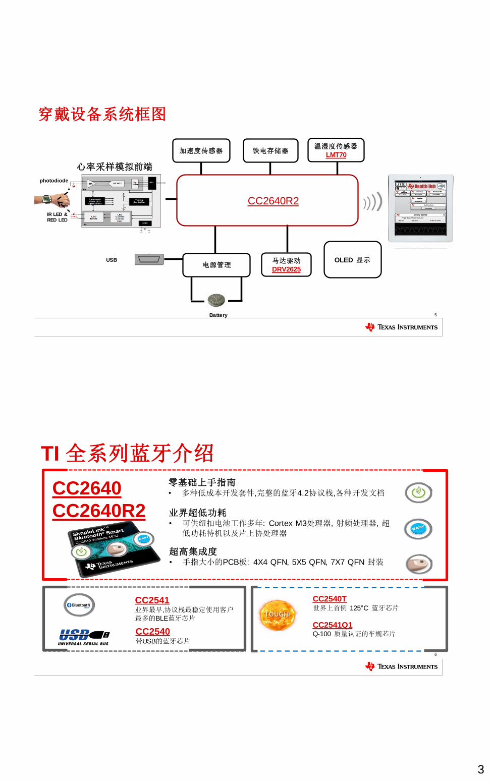
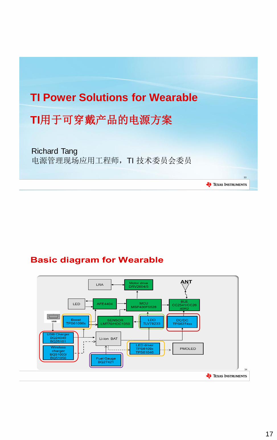
穿戴设备系统框图
5
加速度传感器 铁电存储器
photodiode
IR LED & RED LED
心率采样模拟前端
电源管理 USB
Battery
马达驱动
DRV2625
OLED 显示
温湿度传感器
LMT70
CC2640R2
TI 全系列蓝牙介绍
6
CC2540T
世界上首例 125°C 蓝牙芯片
CC2541Q1 Q-100 质量认证的车规芯片
CC2540 带USB的蓝牙芯片
CC2640
CC2640R2 业界超低功耗 • 可供纽扣电池工作多年: Cortex M3处理器, 射频处理器, 超
低功耗待机以及片上协处理器
超高集成度 • 手指大小的PCB板: 4X4 QFN, 5X5 QFN, 7X7 QFN 封装
零基础上手指南 • 多种低成本开发套件,完整的蓝牙4.2协议栈,各种开发文档
CC2541 业界最早,协议栈最稳定使用客户最多的BLE蓝牙芯片
4
7
蓝牙协议栈
应用层 ~80+ kB
操作系统
TI CC2640R2
RO
M
FLA
SH
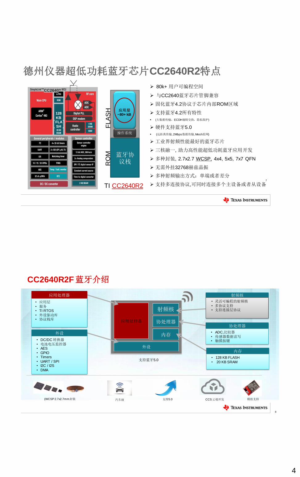
德州仪器超低功耗蓝牙芯片CC2640R2特点
80k+ 用户可编程空间
与CC2640蓝牙芯片管脚兼容
固化蓝牙4.2协议于芯片内部ROM区域
支持蓝牙4.2所有特性
(大数据传输,ECDH秘钥交换,隐私保护)
硬件支持蓝牙5.0
(远距离传输, 2Mbps数据传输, Mesh组网)
工业界射频性能最好的蓝牙芯片
三核融一, 助力高性能超低功耗蓝牙应用开发
多种封装, 2.7x2.7 WCSP, 4x4, 5x5, 7x7 QFN
无需外挂32768赫兹晶振
多种射频输出方式:单端或者差分
支持多连接协议,可同时连接多个主设备或者从设备
CC2640
128
KB FLA
SH
CC2640R2F 蓝牙介绍
8
支持蓝牙5.0
应用处理器
射频核
协处理器
外设
应用处理器
• 应用层
• 服务 • TI RTOS
• 外设驱动库 • 协议栈库
外设
• DC/DC 转换器
• 电池电压监控器 • AES
• GPIO • Timers
• UART / SPI • I2C / I2S
• DMA
协处理器
• ADC,比较器
• 传感器数据读写 • 触摸按键
射频核
• 灵活可编程的射频核
• 多协议支持 • 支持连接层协议
内存
内存
• 128 KB FLASH
• 20 KB SRAM
(WCSP 2.7x2.7mm封装 汽车级 支持5.0 模组支持 CCS 云端开发
5
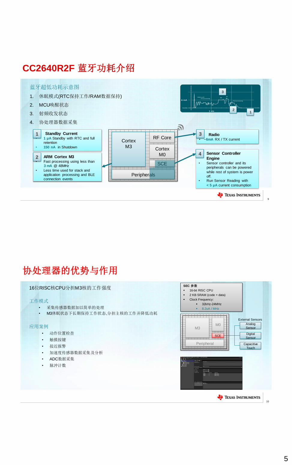
蓝牙超低功耗示意图
1. 休眠模式(RTC保持工作/RAM数据保持)
2. MCU唤醒状态
3. 射频收发状态
4. 协处理器数据采集
Application Note SWRA478: Measuring Bluetooth Smart Power Consumption
9
Cortex
M3
Cortex
M0
SCE
Peripherals
RF Core
• ARM Cortex M3 • Fast processing using less than
3 mA @ 48MHz
• Less time used for stack and
application processing and BLE
connection events
• Sensor Controller
Engine • Sensor controller and its
peripherals can be powered
while rest of system is power
off.
• Run Sensor Reading with
< 5 µA current consumption
• Radio • ~6mA RX / TX current
• Standby Current • 1 µA Standby with RTC and full
retention
• 150 nA in Shutdown
1
2
3
4
1
3
2
CC2640R2F 蓝牙功耗介绍
协处理器的优势与作用
10
16位RISC核CPU分担M3核的工作强度
工作模式
• 采集传感器数据加以简单的处理
• M3休眠状态下长期保持工作状态,分担主核的工作并降低功耗
应用案例
• 动作位置检查
• 触摸按键
• 接近报警
• 加速度传感器数据采集及分析
• ADC数据采集
• 脉冲计数
SEC 参数
16-bit RISC CPU
2 KB SRAM (code + data)
Clock Frequency:
32kHz-24MHz
8.2uA / MHz
M3 M0
SCE
Peripheral
Analog
Sensor
Digital
Sensor
Capacitive
Touch
External Sensors
6
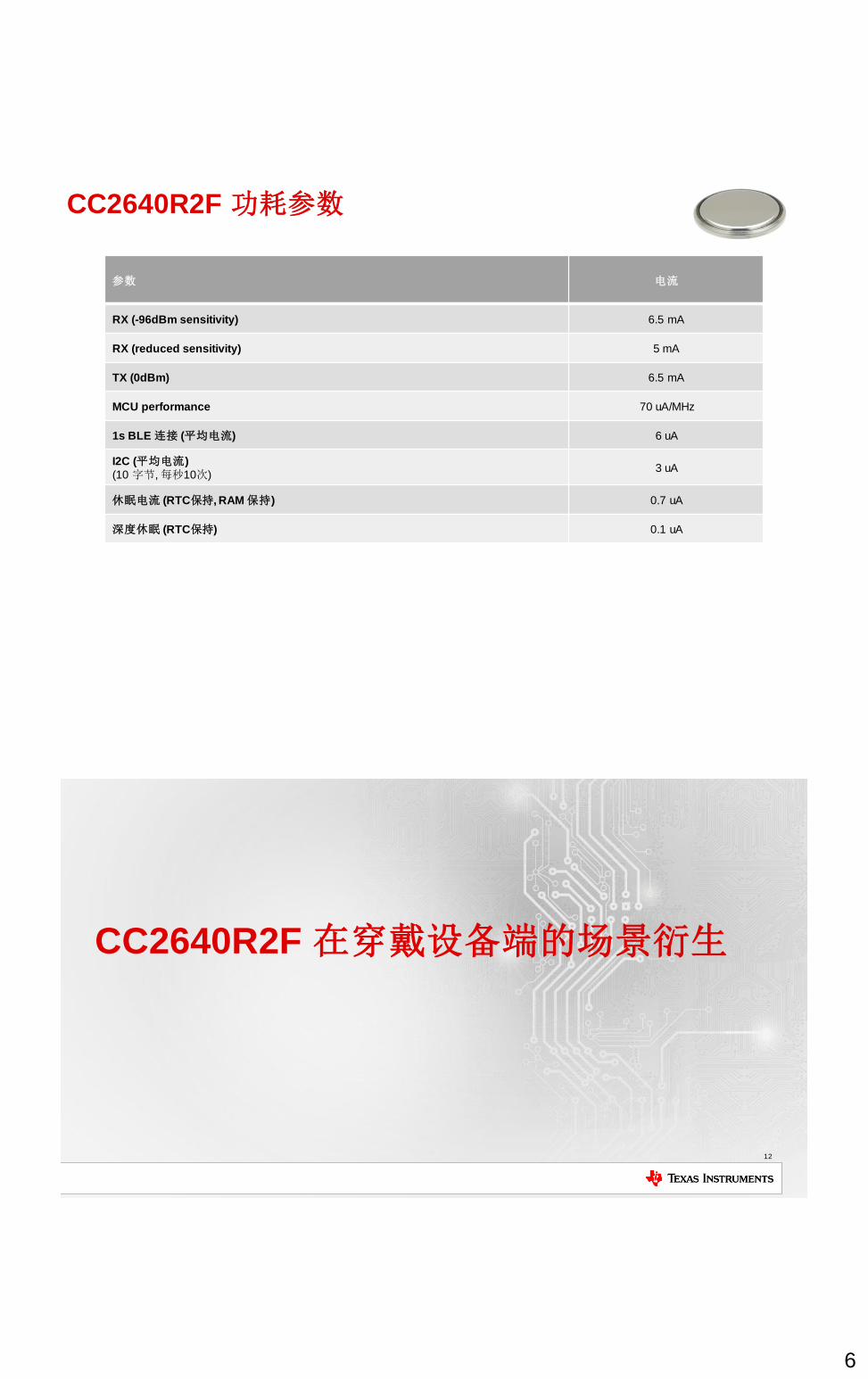
参数 电流
RX (-96dBm sensitivity) 6.5 mA
RX (reduced sensitivity) 5 mA
TX (0dBm) 6.5 mA
MCU performance 70 uA/MHz
1s BLE 连接 (平均电流) 6 uA
I2C (平均电流)
(10 字节, 每秒10次) 3 uA
休眠电流 (RTC保持, RAM 保持) 0.7 uA
深度休眠 (RTC保持) 0.1 uA
CC2640R2F 功耗参数
CC2640R2F 在穿戴设备端的场景衍生
12
7
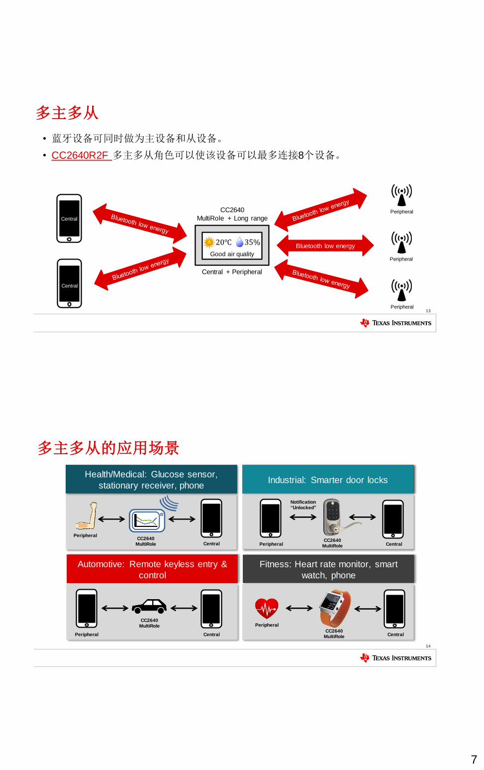
多主多从
• 蓝牙设备可同时做为主设备和从设备。
• CC2640R2F 多主多从角色可以使该设备可以最多连接8个设备。
13
Bluetooth low energy
Central + Peripheral
CC2640
MultiRole + Long range
20℃ 35%
Good air quality
Central
Central
Peripheral
Peripheral
Peripheral
Fitness: Heart rate monitor, smart
watch, phone
Automotive: Remote keyless entry &
control
多主多从的应用场景
14
Health/Medical: Glucose sensor,
stationary receiver, phone Industrial: Smarter door locks
Peripheral
Peripheral
Peripheral
Peripheral
Central Central
Central Central
CC2640 MultiRole
CC2640 MultiRole
CC2640 MultiRole
CC2640 MultiRole
Notification “Unlocked”
8
15
多主多从在穿戴设备的应用
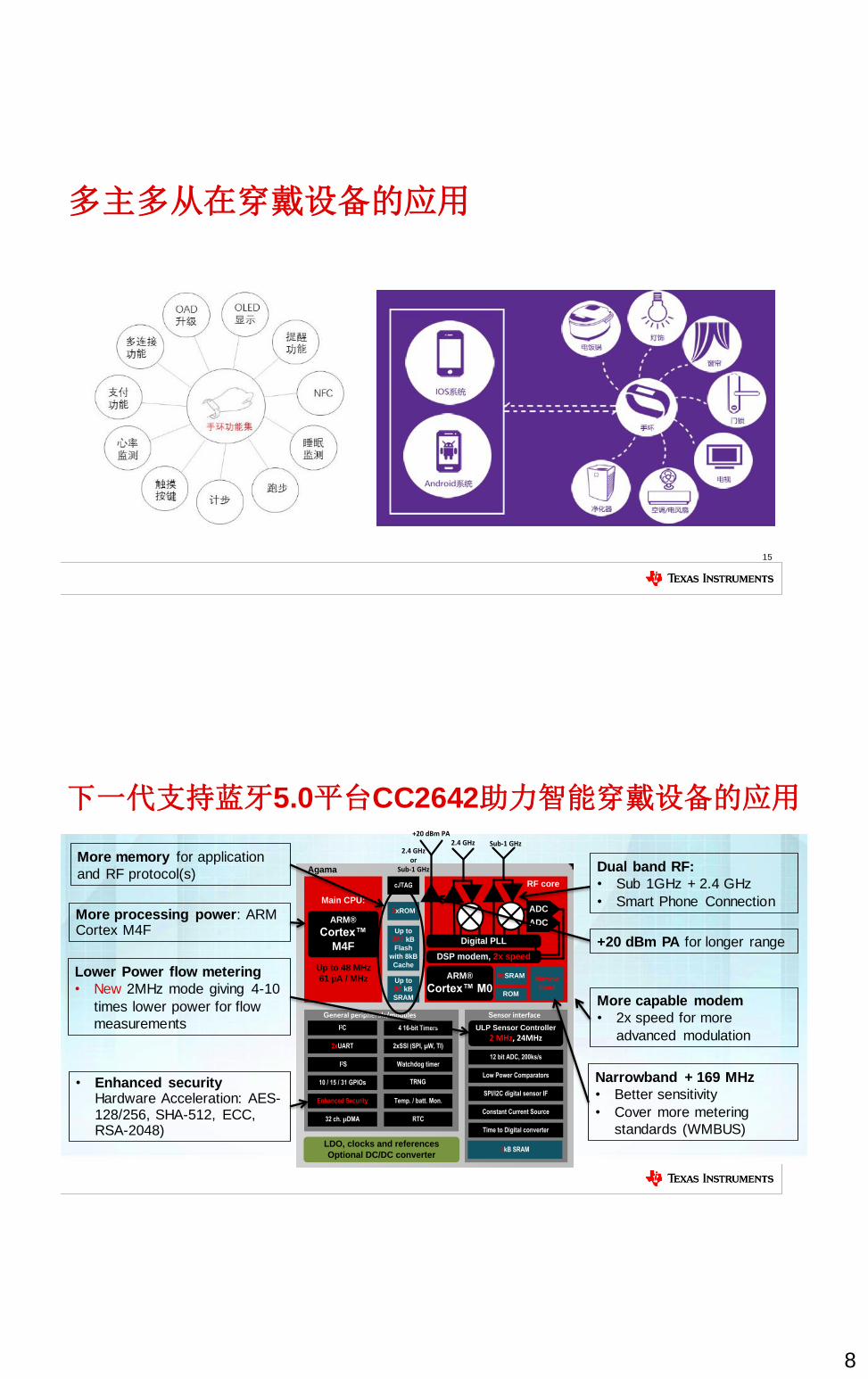
下一代支持蓝牙5.0平台CC2642助力智能穿戴设备的应用
Agama
Main CPU:
Up to
352 kB
Flash
with 8kB
Cache
Sensor interface
cJTAG
Up to
80 kB
SRAM
2xROM
ARM®
Cortex™
M4F
LDO, clocks and references
Optional DC/DC converter
RF core
ARM®
Cortex™ M0
DSP modem, 2x speed
4xSRAM
ROM
ULP Sensor Controller
2 MHz, 24MHz
Low Power Comparators
12 bit ADC, 200ks/s
Constant Current Source
SPI/I2C digital sensor IF
4kB SRAM
Time to Digital converter
General peripherals/modules
4 16-bit Timers
2xSSI (SPI, µW, TI)
Watchdog timer
Temp. / batt. Mon.
RTC
I2C
2xUART
I2S
10 / 15 / 31 GPIOs
Enhanced Security
32 ch. µDMA
ADC
ADC
Digital PLL
Up to 48 MHz
61 µA / MHz
Sub-1 GHz
+20 dBm PA
TRNG
2.4 GHz
Narrow
band
2.4 GHzor
Sub-1 GHz
More memory for application
and RF protocol(s)
More processing power: ARM Cortex M4F
• Enhanced security Hardware Acceleration: AES-128/256, SHA-512, ECC, RSA-2048)
Dual band RF:
• Sub 1GHz + 2.4 GHz
• Smart Phone Connection
More capable modem
• 2x speed for more
advanced modulation
+20 dBm PA for longer range
Narrowband + 169 MHz
• Better sensitivity
• Cover more metering
standards (WMBUS)
Lower Power flow metering
• New 2MHz mode giving 4-10
times lower power for flow
measurements
9
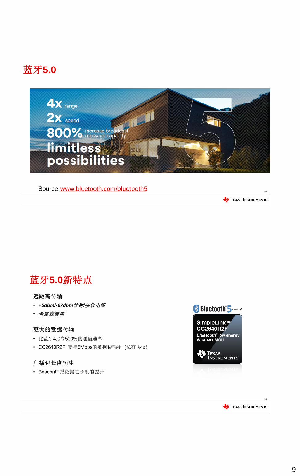
蓝牙5.0
17 Source www.bluetooth.com/bluetooth5
蓝牙5.0新特点
远距离传输
• +5dbm/-97dbm发射/接收电流
• 全家庭覆盖
更大的数据传输
• 比蓝牙4.0高500%的通信速率
• CC2640R2F 支持5Mbps的数据传输率 (私有协议)
广播包长度衍生
• Beacon广播数据包长度的提升
18
10
CC2640R2F蓝牙设计要点
19
20
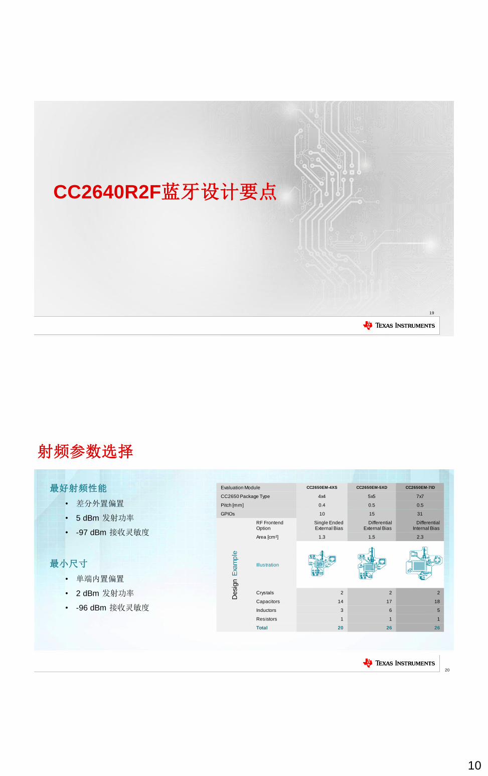
Evaluation Module CC2650EM-4XS CC2650EM-5XD CC2650EM-7ID
CC2650 Package Type 4x4 5x5 7x7
Pitch [mm] 0.4 0.5 0.5
GPIOs 10 15 31
Desig
n E
xam
ple
RF Frontend Option
Single Ended External Bias
Differential External Bias
Differential Internal Bias
Area [cm²] 1.3 1.5 2.3
Illustration
Crystals 2 2 2
Capacitors 14 17 18
Inductors 3 6 5
Resistors 1 1 1
Total 20 26 26
射频参数选择
最好射频性能
• 差分外置偏置
• 5 dBm 发射功率
• -97 dBm 接收灵敏度
最小尺寸
• 单端内置偏置
• 2 dBm 发射功率
• -96 dBm 接收灵敏度
11
21
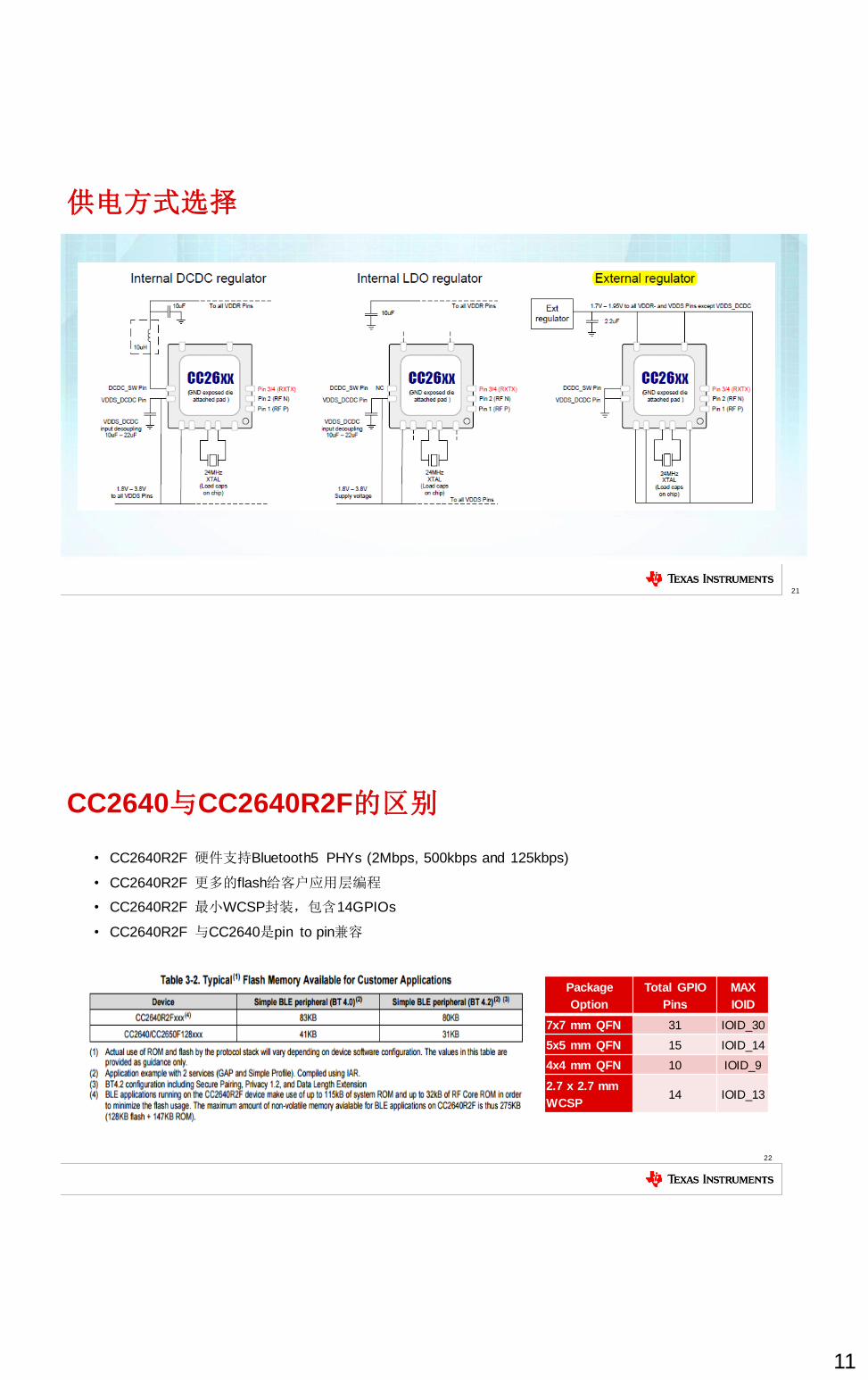
供电方式选择
CC2640与CC2640R2F的区别
• CC2640R2F 硬件支持Bluetooth5 PHYs (2Mbps, 500kbps and 125kbps)
• CC2640R2F 更多的flash给客户应用层编程
• CC2640R2F 最小WCSP封装,包含14GPIOs
• CC2640R2F 与CC2640是pin to pin兼容
22
Package
Option
Total GPIO
Pins
MAX
IOID
7x7 mm QFN 31 IOID_30
5x5 mm QFN 15 IOID_14
4x4 mm QFN 10 IOID_9
2.7 x 2.7 mm
WCSP 14 IOID_13
12
v
CC2640R2F文档
• Fully Qualified BT4.2 Protocol Stack
– All features included
• IDE Support
– IAR Embedded Workbench for AMR v7.80
– Code Composer Studio (CCS) v7.0
• TI-RTOS
– Simplified Management
– Pre-emptive Multit-hreaded environment
• Documentation
– Software Developers Guide
– TI-RTOS Document Overview
– OAD for CC26xx
– Vendor Specific HCI & SimpleNP API Guides
23
4.2
24
IDE’s:
Code
Composer
Studio
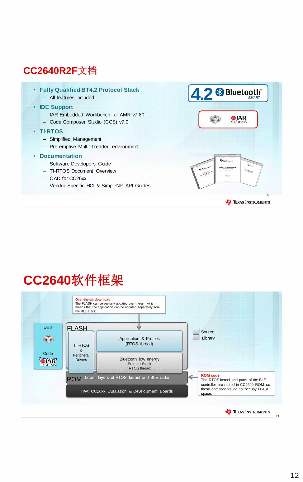
CC2640软件框架
Application & Profiles
(RTOS thread)
HW: CC26xx Evaluation & Development Boards
Source
Library
Lower layers of RTOS kernel and BLE radio
FLASH
ROM
Over-the-air download
The FLASH can be partially updated over-the-air, which means that the application can be updated separately from
the BLE stack.
ROM code
The RTOS kernel and parts of the BLE
controller are stored in CC2640 ROM, so
these components do not occupy FLASH
space.
TI RTOS
& Peripheral
Drivers Bluetooth low energy Protocol Stack
(RTOS thread)
Lower layers of RTOS kernel and BLE radio
13
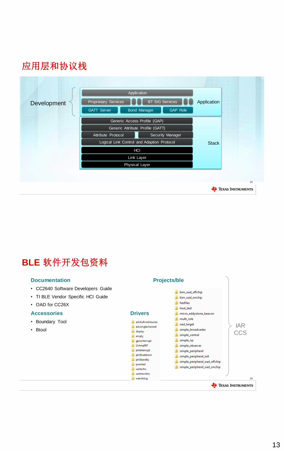
应用层和协议栈
25
Stack
Generic Access Profile (GAP)
Generic Attribute Profile (GATT)
Attribute Protocol Security Manager
Logical Link Control and Adaption Protocol
Link Layer
Physical Layer
HCI
Application
Application
Bond Manager GAP Role GATT Server
BT SIG Services Proprietary Services Development
BLE 软件开发包资料
26
Documentation Projects/ble
• CC2640 Software Developers Guide
• TI BLE Vendor Specific HCI Guide
• OAD for CC26X
Accessories Drivers
• Boundary Tool
• Btool
IAR
CCS
14
软件开发包例程介绍
27
• Example project for a BLE Peripheral Role Device
• What is a BLE Peripheral Device?
– An advertiser that is connectable
– Operates as a slave in a connection
– Example: Heart Rate Sensor
• Implements a GATT Server
– Makes it a Bluetooth SMART candidate
– Both Bluetooth SIG Qualified and Proprietary Profiles
• Excellent for a base product when implementing a BLE device with
a peripheral role purpose. Master
(Central Role)
Slave
(Peripheral Role)
工程软件浏览
28
• Project Workspace in CCS and IAR Embedded Workbench
Application
Profiles
RTOS
BLE Stack
Switch between
App/Stack
15
29
TI-RTOS
C:\ti\tirtos_simplelink_
3_11_00_09
CC26xx-
Ware
SYS/BIOS
Kernel
Drivers Sample
board-files
IDE
Project
Stack
image
Application
image
CC26xx Other device
(iOS, BTool, TI Device
Monitor)
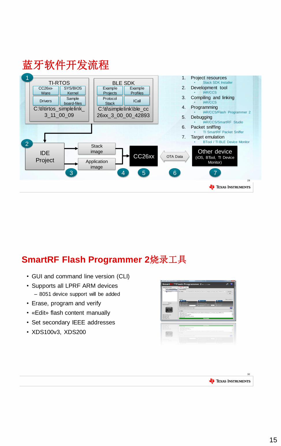
1. Project resources • Stack SDK Installer
2. Development tool • IAR/CCS
3. Compiling and linking • IAR/CCS
4. Programming • IAR/CCS/Flash Programmer 2
5. Debugging • IAR/CCS/SmartRF Studio
6. Packet sniffing • TI SmartRF Packet Sniffer
7. Target emulation • BTool / TI BLE Device Monitor
1
蓝牙软件开发流程
BLE SDK
C:\ti\simplelink\ble_cc
26xx_3_00_00_42893
Example
Projects
Example
Profiles
Protocol
Stack ICall
2
3 4
OTA Data
5 6 7
SmartRF Flash Programmer 2烧录工具
• GUI and command line version (CLI)
• Supports all LPRF ARM devices
– 8051 device support will be added
• Erase, program and verify
• «Edit» flash content manually
• Set secondary IEEE addresses
• XDS100v3, XDS200
30
16
TI 在线资源
31
产品支持
维基百科: www.ti.com/ble-wiki
官网: www.ti.com/ble • Application Notes
• Software & Tools Downloads and Updates
• Order Evaluation and Development Kits
工程师论坛 TI Bluetooth low energy forum – www.ti.com/wiconforum
• http://www.deyisuppport/question_answer (Chinese language, check with Tracy Zhou)
产品认证 • http://processors.wiki.ti.com/index.php/How_to_Certify_your_Bluetooth_product
32
17
TI Power Solutions for Wearable TI用于可穿戴产品的电源方案
33
Richard Tang
电源管理现场应用工程师,TI 技术委员会委员
34
18
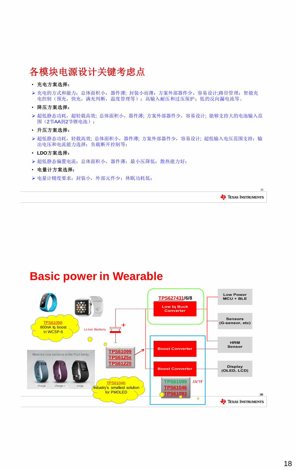
各模块电源设计关键考虑点 • 充电方案选择:
充电的方式和能力;总体面积小,器件薄; 封装小而薄;方案外部器件少,容易设计;路径管理;智能充电控制(预充,快充,满充判断,温度管理等);高输入耐压和过压保护;低的反向漏电流等。
• 降压方案选择:
超低静态功耗,超轻载高效; 总体面积小,器件薄; 方案外部器件少,容易设计; 能够支持大的电池输入范围(2节AA到2节锂电池);
• 升压方案选择:
超低静态功耗,轻载高效; 总体面积小,器件薄; 方案外部器件少,容易设计; 超低输入电压范围支持;输出电压和电流能力选择;负载断开控制等;
• LDO方案选择:
超低静态偏置电流;总体面积小,器件薄;最小压降低;散热能力好;
• 电量计方案选择:
电量计精度要求;封装小,外部元件少;休眠功耗低;
35
36
Basic power in Wearable
36
TPS627431/6/8
TPS61099
TPS6125x
TPS61220
TPS61099
TPS61046
TPS61093
new
TPS61099:
800nA Iq boost
in WCSP-6
TPS61046:
Industry’s smallest solution
for PMOLED
19
37
• VIN Range: 2.0V to 5.5V
• Ultra Low Quiescent Current of typical 360nA
• Up to 90% Efficiency @ 10µA Load Current
• 300mA / 400mA Output Current
• 3 options: a) x43: 8 User Selectable Vout (1.2V, 1.5V,
1.8V, 2.1V, 2.5V, 2.8V, 3.0V, 3.3V)
b) x46: Integrated Vin switch & Selectable Output
Voltages: 1.2V and 1.8V
c) x48: Integrated load switch &Selectable Output
Voltages: 1.2V and 1.8V
d) x431: 1.3V, 1.4V, 1.6V, 1.7V, 1.9V, 2.0V, 2.9V,
3.1V NEW (400mA)
• No Ripple True 100% Mode
TPS62740/3/31/5/6/8 300mA Buck Converter family in QFN, WCSP and module
FEATURES BENEFITS
APPLICATIONS
• MCU, BLE and Sensor Supply
• Wearable Electronics
• Medical Healthcare
• Home Automation
75% package size
reduction
12
ABCD 1.6 mm
0.9
mm
TPS62740
3 mm
2 mm
• RF Friendly DCS-ControlTM
• Discharge VOUT • 3x2 QFN (TPS62740), 1.6 x 0.9 WCSP (TPS62743/6/8) and
SIP module (TPS82740) • Tiny WCSP8 package, 1.6mm x 0.9mm x 0.5mm, Pitch 0.4mm
VIN
EN
VSEL1
VSEL2
VSEL3
SW
VOUT
GND
L 2.2 mH
COUT
10 mF
CIN
10 mF
VIN
2.0V to 5.5V
System
TPS627431.2V
TPS62743/6
new
38
TPS6274x at a Glance
38
TPS62743
VOUT = 1.2V to 3.3V
TPS62746
VOUT = 1.2V & 1.8V
VIN Switch
TPS62748
VOUT = 1.2V & 1.8V
LOAD Switch
0.9 mm
1.6
mm
0.9 mm
1.6
mm
0.9 mm
1.6
mm
20
39
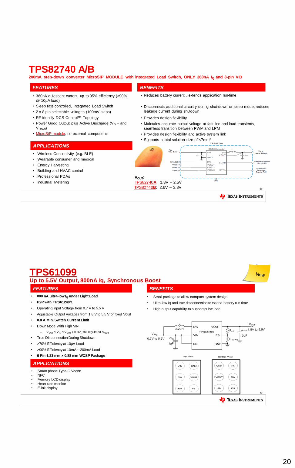
TPS82740 A/B 200mA step-down converter MicroSiP MODULE with integrated Load Switch, ONLY 360nA IQ and 3-pin VID
• Wireless Connectivity (e.g. BLE)
• Wearable consumer and medical
• Energy Harvesting
• Building and HVAC control
• Professional PDAs
• Industrial Metering
VOUT:
TPS82740A: 1.8V – 2.5V
TPS82740B: 2.6V – 3.3V
FEATURES BENEFITS
APPLICATIONS
• Reduces battery current , extends application run-time
• Disconnects additional circuitry during shut-down or sleep mode, reduces
leakage current during shutdown
• Provides design flexibility
• Maintains accurate output voltage at fast line and load transients,
seamless transition between PWM and LPM
• Provides design flexibility and active system link
• Supports a total solution size of <7mm2
• 360nA quiescent current, up to 95% efficiency (>90%
@ 10µA load)
• Sleep rate controlled, integrated Load Switch
• 2 x 8 pin-selectable voltages (100mV steps)
• RF friendly DCS-Control™ Topology
• Power Good Output plus Active Discharge (VOUT and
VLOAD)
• MicroSiP module, no external components
40
TPS61099 Up to 5.5V Output, 800nA Iq, Synchronous Boost
• 800 nA ultra-low IQ under Light Load
• P2P with TPS61240/1
• Operating Input Voltage from 0.7 V to 5.5 V
• Adjustable Output Voltages from 1.8 V to 5.5 V or fixed Vouit
• 0.8 A Min. Switch Current Limit
• Down Mode With High VIN
– VOUT ≤ VIN ≤ VOUT + 0.3V, still regulated VOUT
• True Disconnection During Shutdown
• >70% Efficiency at 10µA Load
• >90% Efficiency at 10mA ~ 200mA Load
• 6 Pin 1.23 mm x 0.88 mm WCSP Package
• Small package to allow compact system design
• Ultra low Iq and true disconnection to extend battery run time
• High output capability to support pulse load
• Smart phone Type-C Vconn
• NFC • Memory LCD display
• Heart rate monitor • E-ink display
GND VIN
VOUT SW
FB EN
Bottom View
GNDVIN
VOUTSW
FBEN
Top View
FEATURES BENEFITS
APPLICATIONS
21
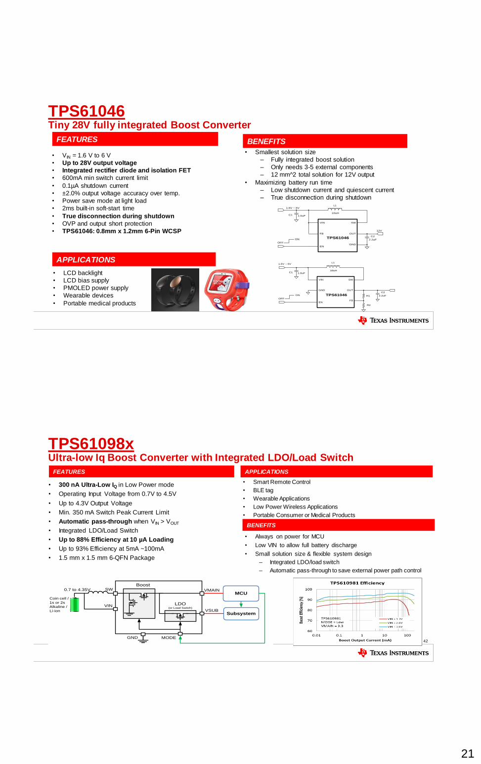
TPS61046 Tiny 28V fully integrated Boost Converter
• VIN = 1.6 V to 6 V
• Up to 28V output voltage
• Integrated rectifier diode and isolation FET
• 600mA min switch current limit
• 0.1µA shutdown current
• ±2.0% output voltage accuracy over temp.
• Power save mode at light load
• 2ms built-in soft-start time
• True disconnection during shutdown
• OVP and output short protection
• TPS61046: 0.8mm x 1.2mm 6-Pin WCSP
• Smallest solution size
– Fully integrated boost solution
– Only needs 3-5 external components
– 12 mm^2 total solution for 12V output
• Maximizing battery run time
– Low shutdown current and quiescent current
– True disconnection during shutdown
• LCD backlight
• LCD bias supply
• PMOLED power supply
• Wearable devices
• Portable medical products
VIN
EN
SW
OUT
FB
GND
L1
2.2uF
1.0uF
R1
R2
OFF
ON
C1
C2
1.6V ~ 6V
10uH
TPS61046
VIN
EN
SW
OUT
GND
FB
L1
2.2uF
1.0uF
OFF
ON
C1
C2
1.6V ~ 6V
12V
10uH
TPS61046
FEATURES BENEFITS
APPLICATIONS
42
• 300 nA Ultra-Low IQ in Low Power mode
• Operating Input Voltage from 0.7V to 4.5V
• Up to 4.3V Output Voltage
• Min. 350 mA Switch Peak Current Limit
• Automatic pass-through when VIN > VOUT
• Integrated LDO/Load Switch
• Up to 88% Efficiency at 10 µA Loading
• Up to 93% Efficiency at 5mA ~100mA
• 1.5 mm x 1.5 mm 6-QFN Package
APPLICATIONS
TPS61098x Ultra-low Iq Boost Converter with Integrated LDO/Load Switch
• Always on power for MCU
• Low VIN to allow full battery discharge
• Small solution size & flexible system design
– Integrated LDO/load switch
– Automatic pass-through to save external power path control
• Smart Remote Control
• BLE tag
• Wearable Applications
• Low Power Wireless Applications
• Portable Consumer or Medical Products
FEATURES
BENEFITS
Subsystem
MCUVMAIN
VSUB
VIN
MODE
0.7 to 4.35V SW
GND
Coin cell /
1s or 2s
Alkaline /
Li-ion
Boost
LDO (or Load Switch)
22
43
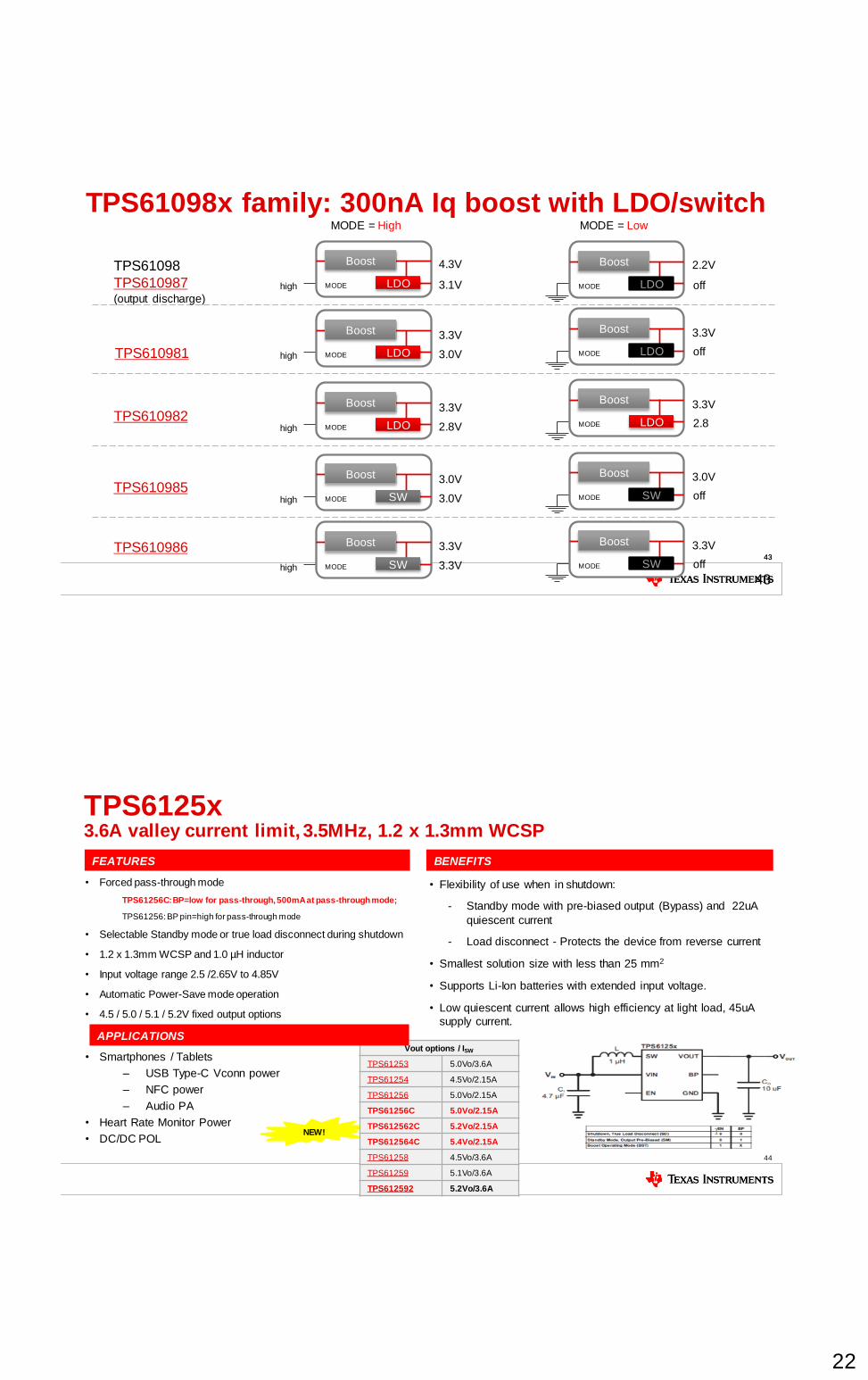
TPS61098x family: 300nA Iq boost with LDO/switch
43
43
MODE LDO
Boost 4.3V
3.1V high MODE LDO
Boost 2.2V
off
MODE LDO
Boost 3.3V
3.0V high MODE LDO
Boost 3.3V
off
MODE LDO
Boost 3.3V
2.8V high MODE LDO
Boost 3.3V
2.8
MODE SW
Boost 3.0V
3.0V high MODE SW
Boost 3.0V
off
MODE SW
Boost 3.3V
3.3V high MODE SW
Boost 3.3V
off
TPS61098
TPS610987 (output discharge)
TPS610981
TPS610982
TPS610985
TPS610986
MODE = High MODE = Low
44
NEW!
• Forced pass-through mode
TPS61256C: BP=low for pass-through, 500mA at pass-through mode;
TPS61256: BP pin=high for pass-through mode
• Selectable Standby mode or true load disconnect during shutdown
• 1.2 x 1.3mm WCSP and 1.0 µH inductor
• Input voltage range 2.5 /2.65V to 4.85V
• Automatic Power-Save mode operation
• 4.5 / 5.0 / 5.1 / 5.2V fixed output options
TPS6125x 3.6A valley current limit, 3.5MHz, 1.2 x 1.3mm WCSP
• Smartphones / Tablets
– USB Type-C Vconn power
– NFC power
– Audio PA
• Heart Rate Monitor Power
• DC/DC POL
• Flexibility of use when in shutdown:
- Standby mode with pre-biased output (Bypass) and 22uA
quiescent current
- Load disconnect - Protects the device from reverse current
• Smallest solution size with less than 25 mm2
• Supports Li-Ion batteries with extended input voltage.
• Low quiescent current allows high efficiency at light load, 45uA
supply current.
Vout options / ISW
TPS61253 5.0Vo/3.6A
TPS61254 4.5Vo/2.15A
TPS61256 5.0Vo/2.15A
TPS61256C 5.0Vo/2.15A
TPS612562C 5.2Vo/2.15A
TPS612564C 5.4Vo/2.15A
TPS61258 4.5Vo/3.6A
TPS61259 5.1Vo/3.6A
TPS612592 5.2Vo/3.6A
FEATURES BENEFITS
APPLICATIONS
23
45
Benefits
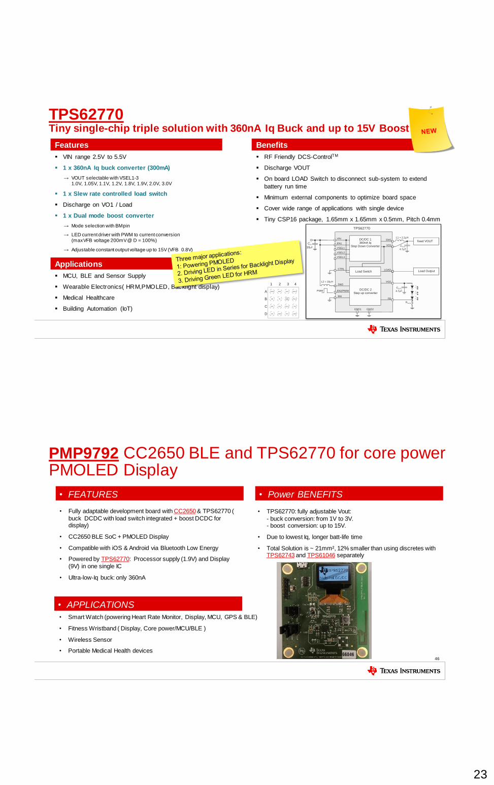
TPS62770 Tiny single-chip triple solution with 360nA Iq Buck and up to 15V Boost
45
Applications
Features
VIN range 2.5V to 5.5V
1 x 360nA Iq buck converter (300mA)
→ VOUT selectable with VSEL1-3 1.0V, 1.05V, 1.1V, 1.2V, 1.8V, 1.9V, 2.0V, 3.0V
1 x Slew rate controlled load switch
Discharge on VO1 / Load
1 x Dual mode boost converter
→ Mode selection with BM pin
→ LED current driver with PWM to current conversion (max VFB voltage 200mV @ D = 100%)
→ Adjustable constant output voltage up to 15V (VFB 0.8V)
MCU, BLE and Sensor Supply
Wearable Electronics( HRM,PMOLED, Backlight display)
Medical Healthcare
Building Automation (IoT)
RF Friendly DCS-ControlTM
Discharge VOUT
On board LOAD Switch to disconnect sub-system to extend
battery run time
Minimum external components to optimize board space
Cover wide range of applications with single device
Tiny CSP16 package, 1.65mm x 1.65mm x 0.5mm, Pitch 0.4mm
SW2
VIN
EN2/PWM
VO2L2 = 10 Hm
COUT2
4.7 Fm
C
10IN
mF
TPS62770
GND1
DC/DC 2 Step up converter
EN1
SW1
VO1
L1 = 2.2 Hm
C
4.7 FOUT1
m
fixed VOUT DC/DC 1360nA Iq
Step Down Converter
CTRL LOAD Load OutputLoad Switch
FB
GND2
VSEL1
VSEL2
VSEL3
BM
PWM
RSense
GND2 SW2 VO2 VSEL3
VSEL2
CTRL
LOADVO1GND1VIN
SW1 EN1 VSEL1
BM FBEN2/PWM
A
B
C
D
1 2 3 4
Top view 16 pin YFF package
46
PMP9792 CC2650 BLE and TPS62770 for core power PMOLED Display
• FEATURES
• Fully adaptable development board with CC2650 & TPS62770 (
buck DCDC with load switch integrated + boost DCDC for display)
• CC2650 BLE SoC + PMOLED Display
• Compatible with iOS & Android via Bluetooth Low Energy
• Powered by TPS62770: Processor supply (1.9V) and Display
(9V) in one single IC
• Ultra-low-Iq buck: only 360nA
• APPLICATIONS
• Smart Watch (powering Heart Rate Monitor, Display, MCU, GPS & BLE)
• Fitness Wristband ( Display, Core power/MCU/BLE )
• Wireless Sensor
• Portable Medical Health devices
• Power BENEFITS
• TPS62770: fully adjustable Vout:
- buck conversion: from 1V to 3V. - boost conversion: up to 15V.
• Due to lowest Iq, longer batt-life time
• Total Solution is ~ 21mm², 12% smaller than using discretes with TPS62743 and TPS61046 separately
24
47
Ultra Low Iq: 0.5 µA
Drop out Voltage: 130 mV @ 150 mA
Stable with 1µF Ceramic Output Capacitor
TSOT23-5 Package
2x2mm SON 6 Package
Ideal for Power sensitive application
Increased battery life
Small size solution
Low Profile industry standard package
Thermally enhanced packaged 45% smaller than TSOT-
23 package
TI MSP430 Attach applications
Wireless Handsets
Portable Media Players
Battery Operated devices with extended sleep times
TPS782xx 150mA Ultra-Low Iq LDO
EVM
DDC
(SOT23)
3mm x 3mm`
DRV
(SON 6)2mm x 2mm
VOUT
GNDN/C
EN
GND
(Top View)
GND
EN
GND
GND
VOUT
VIN
VIN
3.0V
VSS
VCC
MSP430
Or
Equivalent
VIN
EN
VOUT
GND
TPS782301uF 1uF
ON
OFF
3.6V
Battery
Device VIN IOUT VDO IQ Package
TPS782xx 2.2 – 5.5 150mA 130mV 0.5µA DDC, DRV TPS78230EVM-445
48
bq2404x/5x 1A Linear Charger in 2x2 QFN with D+/D- Based Adapter Detection
• Single input AC/USB Li-Ion charger compatible with mini-USB interface
• 28V maximum input voltage with OVP at 6.5V
• Support applications for very low charge currents (i.e 30 – 50mA and above).
• Automatic AC/USB detection using integrated D+/D- pins (bq24050)
• Adjustable Pre-Charge/Termination Current (5% - 50% ISET)
• V(IN) based current reduction loop for USB applications
• Thermal Regulation Loop: Charge current clamping as die temperature increases
• TS pin to monitor pack temperature (NTC) during charging
– Compatible with JEITA safety standard
• Status pins: CHG, PGOOD
• Fixed pre-charge and safety timers
• 2x2 mm 10 pin thermally enhanced power pad packages
1
2
3
4
5
10
9
8
7
6
IN
ISET
VSS
PRETERM
D+ D-
ISET2
CHG
TS
OUT
bq24050/2
25
49
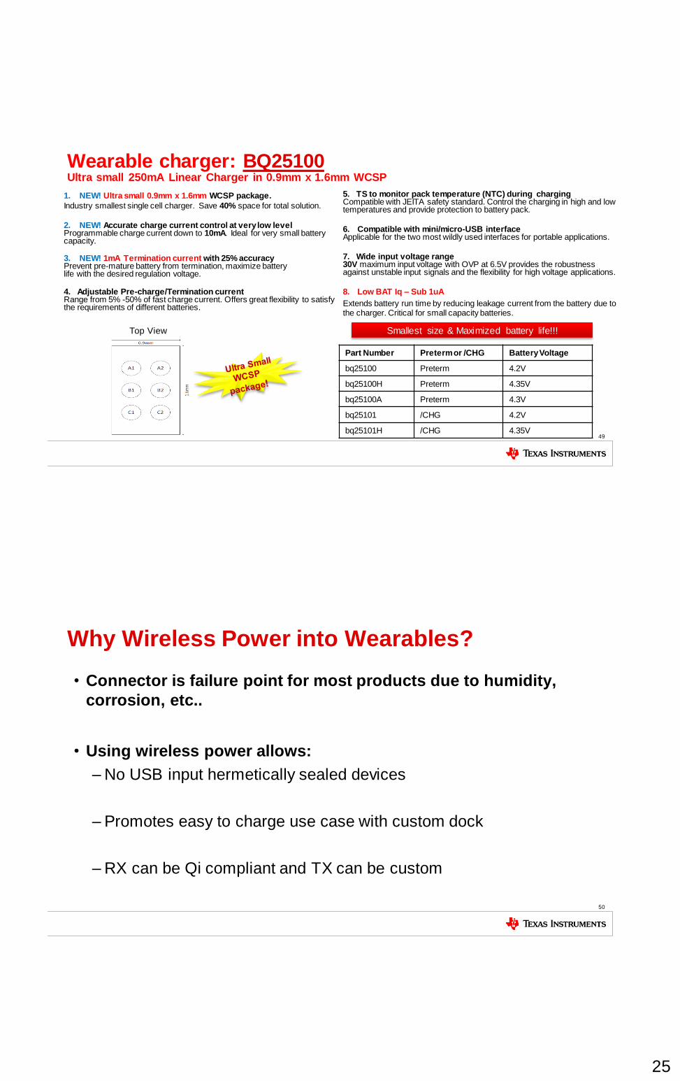
Wearable charger: BQ25100 Ultra small 250mA Linear Charger in 0.9mm x 1.6mm WCSP
1. NEW! Ultra small 0.9mm x 1.6mm WCSP package.
Industry smallest single cell charger. Save 40% space for total solution.
2. NEW! Accurate charge current control at very low level Programmable charge current down to 10mA. Ideal for very small battery capacity. 3. NEW! 1mA Termination current with 25% accuracy Prevent pre-mature battery from termination, maximize battery life with the desired regulation voltage.
4. Adjustable Pre-charge/Termination current Range from 5% -50% of fast charge current. Offers great flexibility to satisfy the requirements of different batteries.
5. TS to monitor pack temperature (NTC) during charging Compatible with JEITA safety standard. Control the charging in high and low temperatures and provide protection to battery pack.
6. Compatible with mini/micro-USB interface Applicable for the two most wildly used interfaces for portable applications.
7. Wide input voltage range 30V maximum input voltage with OVP at 6.5V provides the robustness against unstable input signals and the flexibility for high voltage applications.
8. Low BAT Iq – Sub 1uA
Extends battery run time by reducing leakage current from the battery due to the charger. Critical for small capacity batteries.
Smallest size & Maximized battery life!!!
Part Number Preterm or /CHG Battery Voltage
bq25100 Preterm 4.2V
bq25100H Preterm 4.35V
bq25100A Preterm 4.3V
bq25101 /CHG 4.2V
bq25101H /CHG 4.35V
Top View
50
Why Wireless Power into Wearables?
• Connector is failure point for most products due to humidity,
corrosion, etc..
• Using wireless power allows:
– No USB input hermetically sealed devices
– Promotes easy to charge use case with custom dock
– RX can be Qi compliant and TX can be custom
26
51
52
27
53
53
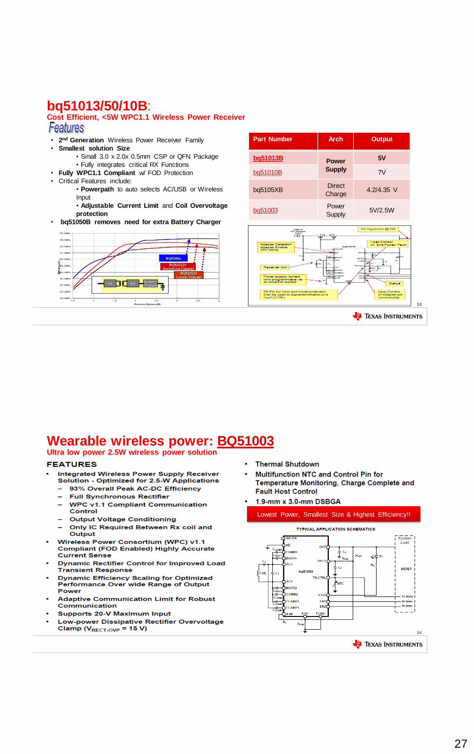
bq51013/50/10B: Cost Efficient, <5W WPC1.1 Wireless Power Receiver
BQ5105x
BQ51013+ Linear Charger
BQ51013+ Switching Charger
TX RX Battery Charger
• 2nd Generation Wireless Power Receiver Family
• Smallest solution Size
• Small 3.0 x 2.0x 0.5mm CSP or QFN Package
• Fully integrates critical RX Functions
• Fully WPC1.1 Compliant w/ FOD Protection
• Critical Features include:
• Powerpath to auto selects AC/USB or Wireless
Input
• Adjustable Current Limit and Coil Overvoltage
protection
• bq51050B removes need for extra Battery Charger
Part Number Arch Output
bq51013B Power
Supply
5V
bq51010B 7V
bq5105XB Direct
Charge 4.2/4.35 V
bq51003 Power
Supply 5V/2.5W
54
Wearable wireless power: BQ51003 Ultra low power 2.5W wireless power solution
Lowest Power, Smallest Size & Highest Efficiency!!
28
55
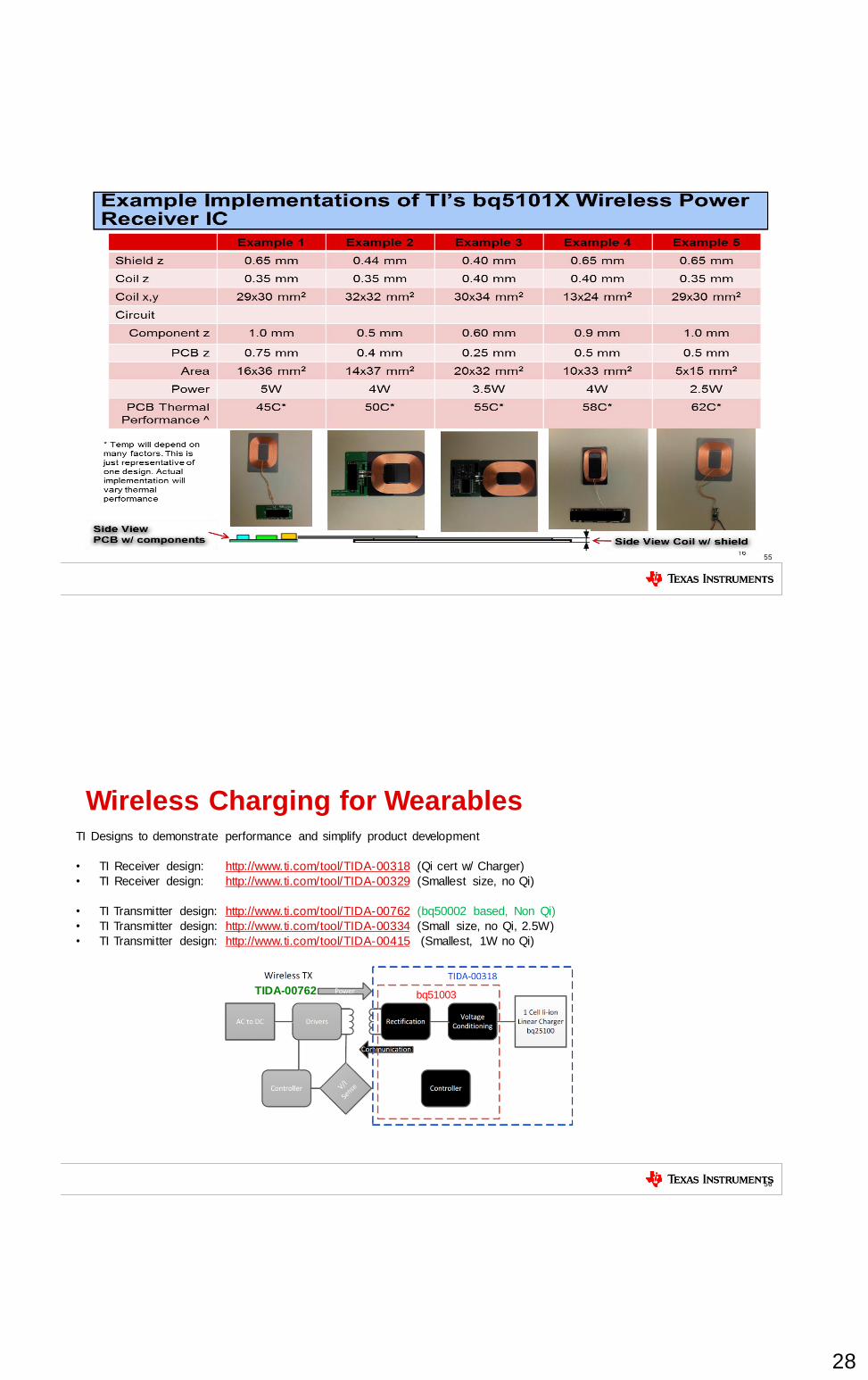
Wireless Charging for Wearables
56
TI Designs to demonstrate performance and simplify product development
• TI Receiver design: http://www.ti.com/tool/TIDA-00318 (Qi cert w/ Charger)
• TI Receiver design: http://www.ti.com/tool/TIDA-00329 (Smallest size, no Qi)
• TI Transmitter design: http://www.ti.com/tool/TIDA-00762 (bq50002 based, Non Qi)
• TI Transmitter design: http://www.ti.com/tool/TIDA-00334 (Small size, no Qi, 2.5W)
• TI Transmitter design: http://www.ti.com/tool/TIDA-00415 (Smallest, 1W no Qi)
bq51003 TIDA-00762
29
57
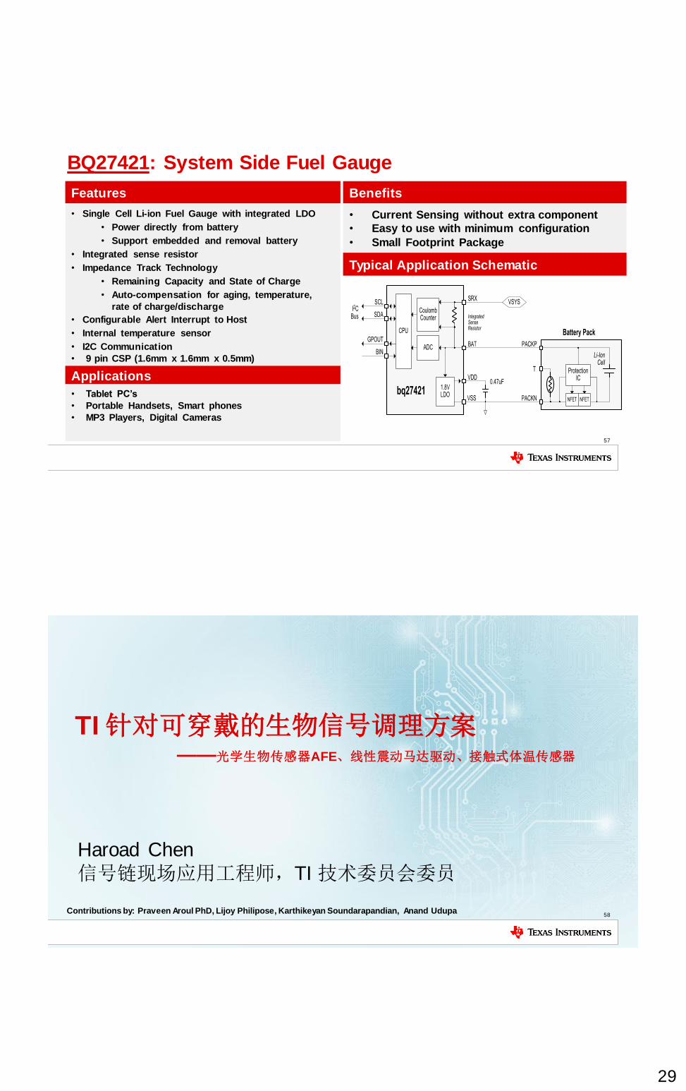
BQ27421: System Side Fuel Gauge
• Single Cell Li-ion Fuel Gauge with integrated LDO
• Power directly from battery
• Support embedded and removal battery
• Integrated sense resistor
• Impedance Track Technology
• Remaining Capacity and State of Charge
• Auto-compensation for aging, temperature,
rate of charge/discharge
• Configurable Alert Interrupt to Host
• Internal temperature sensor
• I2C Communication
• 9 pin CSP (1.6mm x 1.6mm x 0.5mm)
• Current Sensing without extra component
• Easy to use with minimum configuration
• Small Footprint Package
Applications
• Tablet PC’s
• Portable Handsets, Smart phones
• MP3 Players, Digital Cameras
Features Benefits
Typical Application Schematic
TI 针对可穿戴的生物信号调理方案 ——光学生物传感器AFE、线性震动马达驱动、接触式体温传感器
58 Contributions by: Praveen Aroul PhD, Lijoy Philipose, Karthikeyan Soundarapandian, Anand Udupa
Haroad Chen
信号链现场应用工程师,TI 技术委员会委员
30
内容简介
• 原理: PulseOx, Optical HRM
• AFE44XX功能介绍
• HRM系统设计挑战和AFE44XX的解决方案
• TI’s Optical HRM Ecosystem
• TI 线性震动马达和体温传感器介绍
59
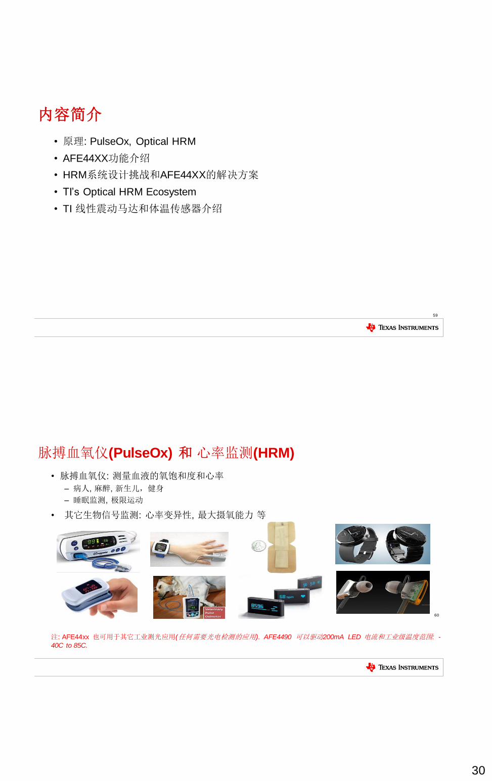
脉搏血氧仪(PulseOx) 和 心率监测(HRM)
• 脉搏血氧仪: 测量血液的氧饱和度和心率
– 病人, 麻醉, 新生儿,健身
– 睡眠监测, 极限运动
• 其它生物信号监测: 心率变异性, 最大摄氧能力 等
注: AFE44xx 也可用于其它工业测光应用(任何需要光电检测的应用). AFE4490 可以驱动200mA LED 电流和工业级温度范围: -
40C to 85C.
60
31
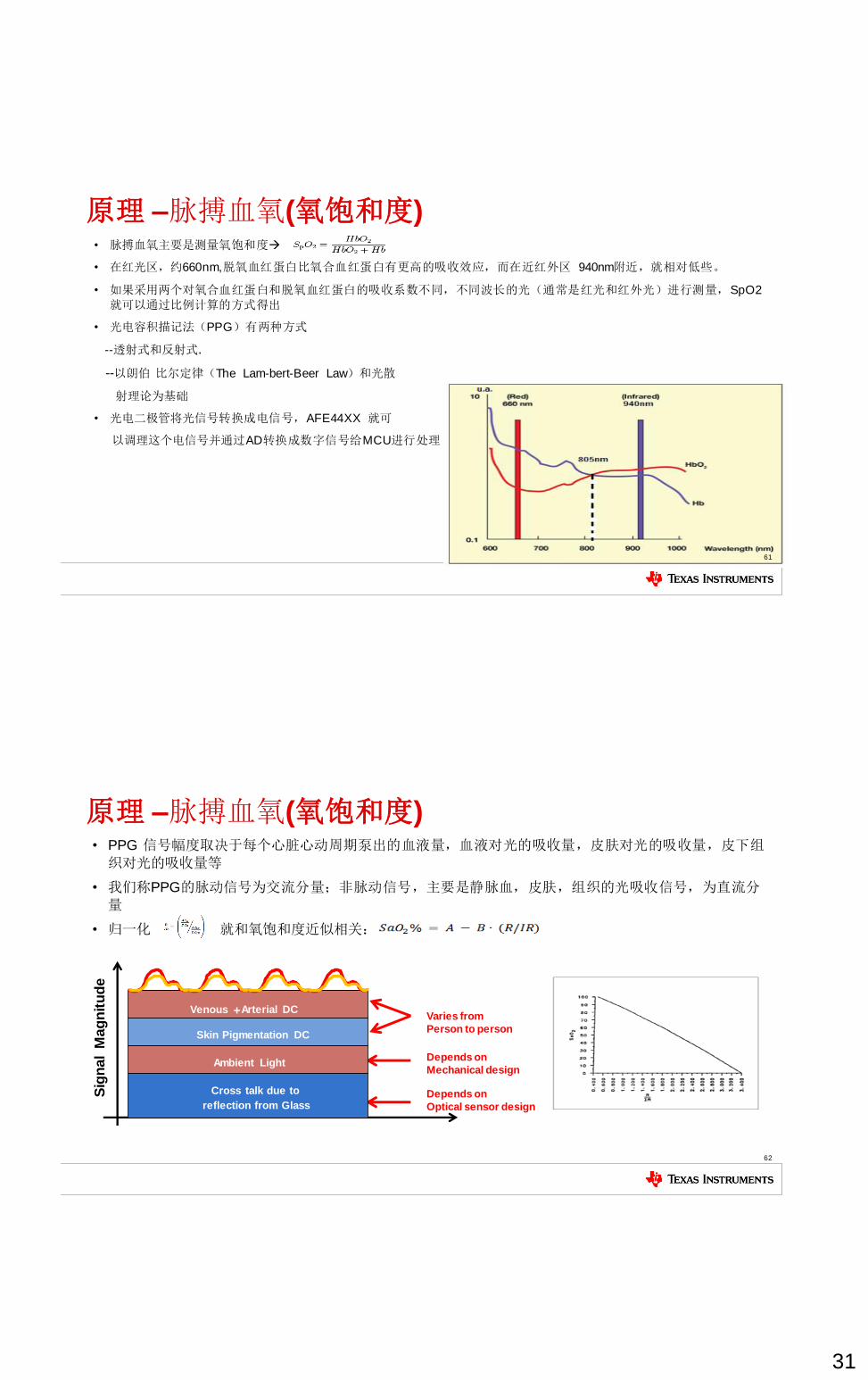
原理 –脉搏血氧(氧饱和度) • 脉搏血氧主要是测量氧饱和度
• 在红光区,约660nm,脱氧血红蛋白比氧合血红蛋白有更高的吸收效应,而在近红外区 940nm附近,就相对低些。
• 如果采用两个对氧合血红蛋白和脱氧血红蛋白的吸收系数不同,不同波长的光(通常是红光和红外光)进行测量,SpO2
就可以通过比例计算的方式得出
• 光电容积描记法(PPG)有两种方式
--透射式和反射式.
--以朗伯 比尔定律(The Lam-bert-Beer Law)和光散
射理论为基础
• 光电二极管将光信号转换成电信号,AFE44XX 就可
以调理这个电信号并通过AD转换成数字信号给MCU进行处理
61
原理 –脉搏血氧(氧饱和度) • PPG 信号幅度取决于每个心脏心动周期泵出的血液量,血液对光的吸收量,皮肤对光的吸收量,皮下组
织对光的吸收量等
• 我们称PPG的脉动信号为交流分量;非脉动信号,主要是静脉血,皮肤,组织的光吸收信号,为直流分量
• 归一化 就和氧饱和度近似相关:
62
Sig
nal
Mag
nit
ud
e
Varies from
Person to person
Depends on
Mechanical design
Depends on
Optical sensor design
Cross talk due to
reflection from Glass
Ambient Light
Skin Pigmentation DC
Venous + Arterial DC
32
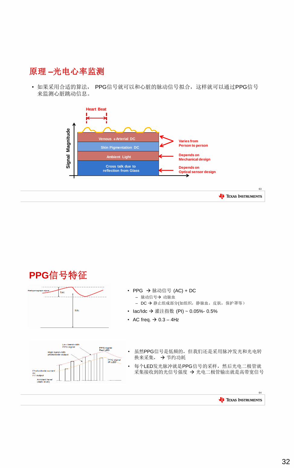
原理 –光电心率监测
• 如果采用合适的算法, PPG信号就可以和心脏的脉动信号拟合,这样就可以通过PPG信号来监测心脏跳动信息。
63
Sig
nal
Mag
nit
ud
e
Varies from
Person to person
Depends on
Mechanical design
Depends on
Optical sensor design
Cross talk due to reflection from Glass
Ambient Light
Skin Pigmentation DC
Venous + Arterial DC
Heart Beat
PPG信号特征
• PPG 脉动信号 (AC) + DC
– 脉动信号 动脉血
– DC 静止组成部分(如组织,静脉血,皮肤,保护罩等)
• Iac/Idc 灌注指数 (PI) ~ 0.05%- 0.5%
• AC freq. 0.3 – 4Hz
64
• 虽然PPG信号是低频的,但我们还是采用脉冲发光和光电转
换来采集, 节约功耗
• 每个LED发光脉冲就是PPG信号的采样,然后光电二极管就采集接收到的光信号强度 光电二极管输出就是高带宽信号
33
65
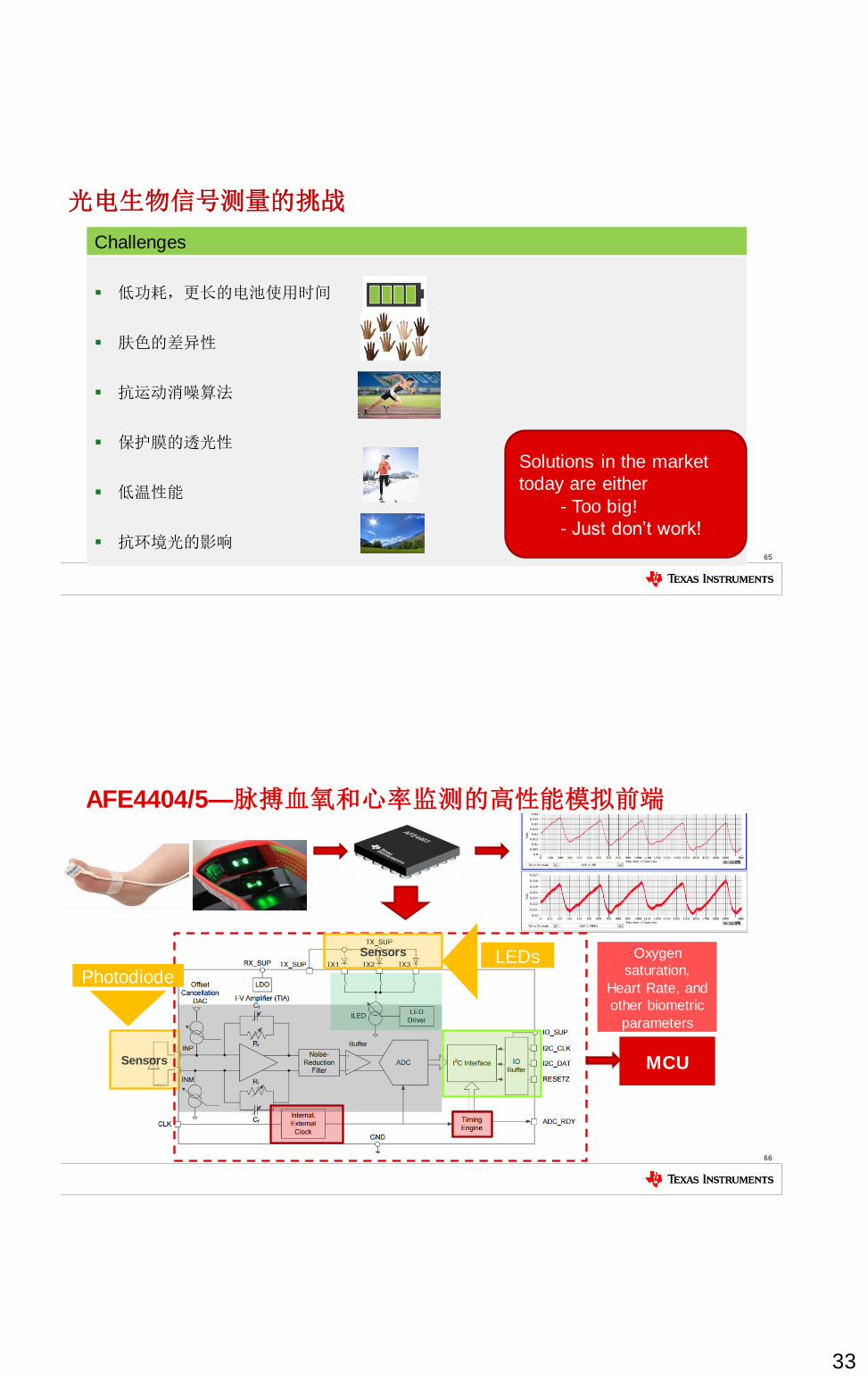
光电生物信号测量的挑战
Challenges
低功耗,更长的电池使用时间
肤色的差异性
抗运动消噪算法
保护膜的透光性
低温性能
抗环境光的影响
Solutions in the market
today are either
- Too big!
- Just don’t work!
AFE4404/5—脉搏血氧和心率监测的高性能模拟前端
66
Sensors
LEDs
MCU
Oxygen
saturation,
Heart Rate, and
other biometric
parameters
Photodiode
Sensors
34
67
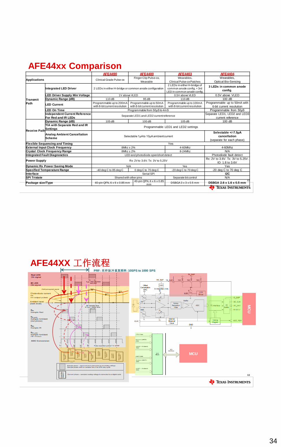
AFE4490 AFE4400 AFE4403 AFE4404
Applications Clinical Grade Pulse-ox Finger Clip Pulse-ox, Wearables, Wearables,
Wearable Clinical Pulse-ox Patches Optical Bio-Sensing
Transmit
Path
Integrated LED Driver 2 LEDs in either H-bridge or common anode configuration 2 LEDs in either H-bridge of common anode config. + 3rd
LED in common anode config.
3 LEDs in common anode
config.
LED Driver Supply Min Voltage 1V above VLED 0.5V above VLED 0.5V above VLED
Dynamic Range (dB) 110 dB 95 dB 110 dB 100 dB
LED Current Programmable up to 200mA with 8-bit current resolution
Programmable up to 50mA with 8-bit current resolution
Programmable up to 100mA with 8-bit current resolution
Programmable up to 50mA with
6-bit current resolution
LED On Time Programmable from 50μS to 4mS Programmable from 50μS
Independent Current Reference
For Red and IR LEDs Separate LED1 and LED2 current reference
Separate LED1, LED2 and LED3
current reference
Receive Path
Dynamic Range (dB) 105 dB 100 dB 105 dB 100 dB
TIA with Separate Red and IR
Settings Programmable LED1 and LED2 settings
Analog Ambient Cancellation
Scheme Selectable 1μA to 10μA ambient current
Selectable +/-7.5μA
cancellation
(separate for each phase)
Flexible Sequencing and Timing Yes
External Input Clock Frequency 8Mhz ± 2% 4-60Mhz 4-60Mhz
Crystal Clock Frequency Range 8Mhz ± 2% 8-24Mhz N/A
Integrated Fault Diagnosctics LED and photodiode open/short detect Photodiode fault detect
Power Supply Rx: 2V to 3.6V. Tx: 3V to 5.25V Rx: 2V to 3.6V. Tx: 3V to 5.25V.
IO: 1.8 to 3.6V
Dynamic Rx Power Saving Mode N/A Yes Yes
Specified Temperature Range -40 deg C to 85 deg C 0 deg C to 70 deg C -20 deg C to 70 deg C -20 deg C to 70 deg C
Interface Serial SPI I2C
SPI Tristate Shared with other pins Separate bit control N/A
Package size/Type 40-pin QFN, 6 x 6 x 0.85 mm 40-pin QFN, 6 x 6 x 0.85
mm DSBGA 3 x 3 x 0.5 mm DSBGA 2.6 x 1.6 x 0.5 mm
AFE44xx Comparison
AFE44XX 工作流程
68
MCU
MC
U
PRF: 采样脉冲重复频率: 10SPS to 1000 SPS
35
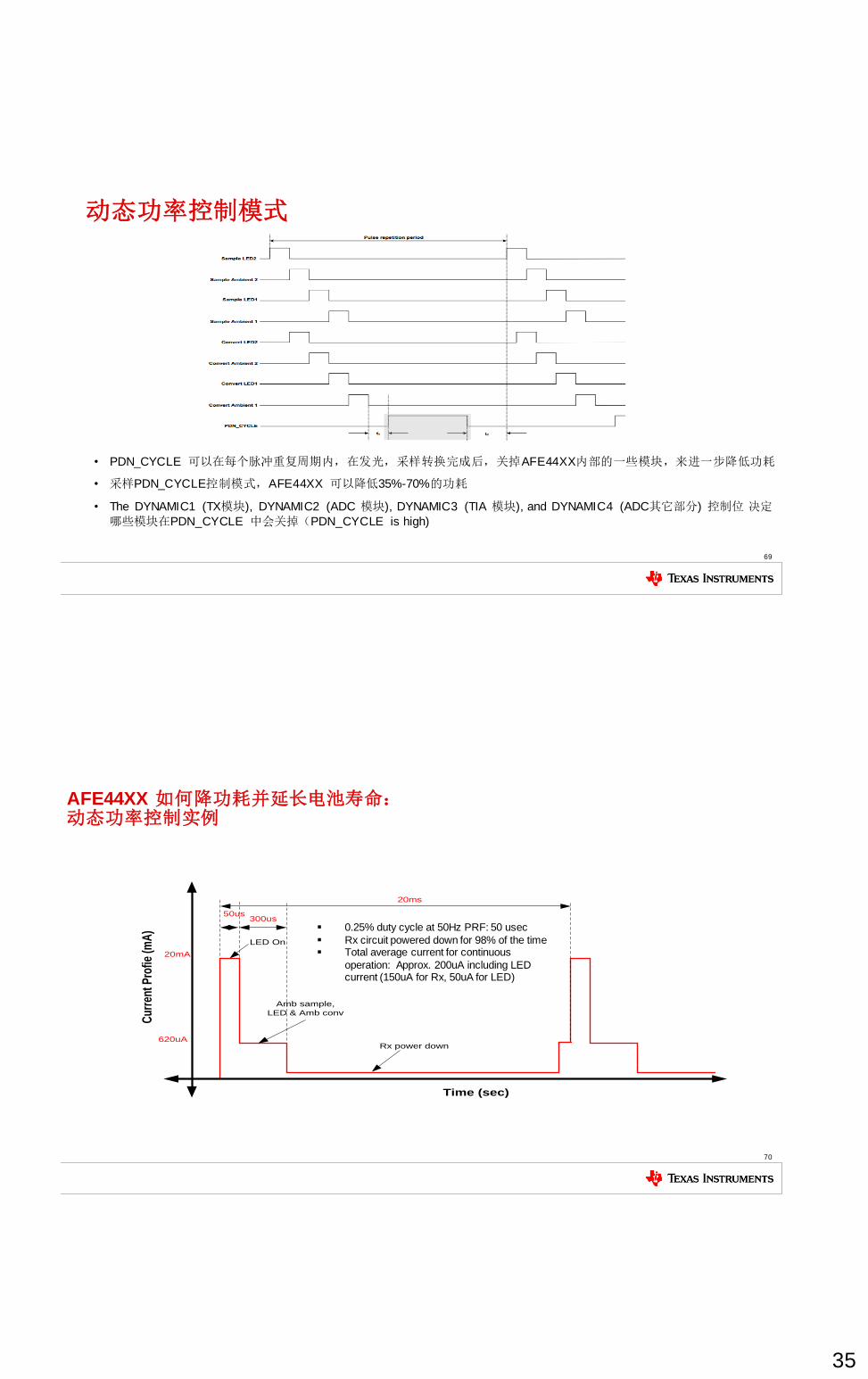
动态功率控制模式
• PDN_CYCLE 可以在每个脉冲重复周期内,在发光,采样转换完成后,关掉AFE44XX内部的一些模块,来进一步降低功耗
• 采样PDN_CYCLE控制模式,AFE44XX 可以降低35%-70%的功耗
• The DYNAMIC1 (TX模块), DYNAMIC2 (ADC 模块), DYNAMIC3 (TIA 模块), and DYNAMIC4 (ADC其它部分) 控制位 决定哪些模块在PDN_CYCLE 中会关掉(PDN_CYCLE is high)
69
AFE44XX 如何降功耗并延长电池寿命: 动态功率控制实例
70
Amb sample,
LED & Amb conv
LED On
Rx power down
50us300us
20ms
Cur
rent
Pro
fie (m
A)
Time (sec)
20mA
620uA
0.25% duty cycle at 50Hz PRF: 50 usec
Rx circuit powered down for 98% of the time Total average current for continuous
operation: Approx. 200uA including LED current (150uA for Rx, 50uA for LED)
36
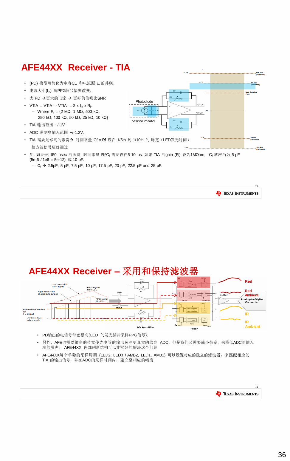
AFE44XX Receiver - TIA
71
Photodiode
• (PD) 模型可简化为电容Cin 和电流源 lin 的并联。
• 电流大小(lin) 随PPG信号幅度改变.
• 大 PD 更大的电流 更好的信噪比SNR
• VTIA = VTIA+ - VTIA- = 2 x lin x Rf.
– Where Rf = {2 MΩ, 1 MΩ, 500 kΩ,
250 kΩ, 100 kΩ, 50 kΩ, 25 kΩ, 10 kΩ}
• TIA 输出范围 +/-1V
• ADC 满刻度输入范围 +/-1.2V.
• TIA 需要足够高的带宽 时间常量 Cf x Rf 设在 1/5th 到 1/10th 的 脉宽(LED发光时间)
使方波信号更好通过
• 如, 如果采用50 usec 的脉宽, 时间常量 Rf*Cf 需要设在5-10 us. 如果 TIA 的gain (Rf) 设为1MOhm, Cf 就应当为 5 pF
(5e-6 / 1e6 = 5e-12) 或 10 pF.
– Cf 2.5pF, 5 pF, 7.5 pF, 10 pF, 17.5 pF, 20 pF, 22.5 pF and 25 pF.
AFE44XX Receiver – 采用和保持滤波器
• PD输出的电信号带宽很高(LED 的发光脉冲采样PPG信号).
• 另外,AFE也需要很高的带宽使光电管的输出脉冲更真实的给到 ADC,但是我们又需要减小带宽, 来降低ADC的输入端的噪声。 AFE44XX 内部创新结构可以非常好的解决这个问题
• AFE44XX每个单独的采样周期 (LED2, LED3 / AMB2, LED1, AMB1) 可以设置对应的独立的滤波器,来匹配相应的
TIA 的输出信号,并在ADC的采样时间内,建立至相应的幅度
72
Red
Red
Ambient
IR
IR
Ambient
37
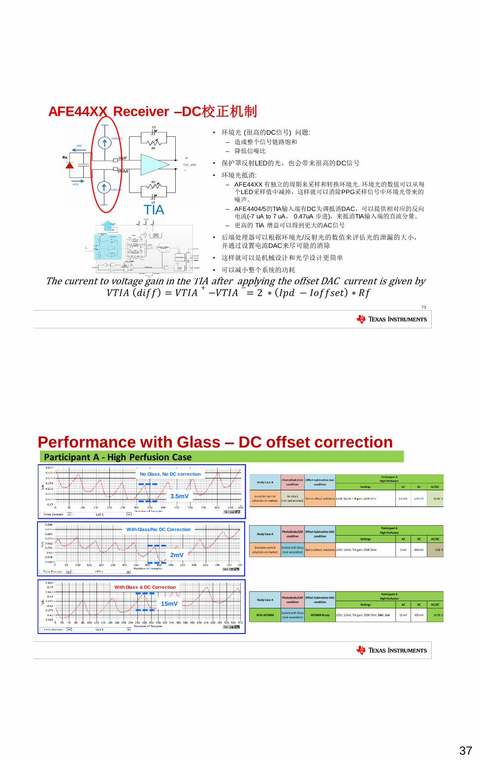
AFE44XX Receiver –DC校正机制
• 环境光 (很高的DC信号) 问题:
– 造成整个信号链路饱和
– 降低信噪比
• 保护罩反射LED的光,也会带来很高的DC信号
• 环境光抵消:
– AFE44XX 有独立的周期来采样和转换环境光. 环境光的数值可以从每个LED采样值中减掉,这样就可以消除PPG采样信号中环境光带来的噪声。
– AFE4404/5的TIA输入端有DC失调抵消DAC,可以提供相对应的反向电流(-7 uA to 7 uA, 0.47uA 步进),来抵消TIA输入端的直流分量。
– 更高的 TIA 增益可以得到更大的AC信号
• 后端处理器可以根据环境光/反射光的数值来评估光的泄漏的大小,并通过设置电流DAC来尽可能的消除
• 这样就可以是机械设计和光学设计更简单
• 可以减小整个系统的功耗
73
The current to voltage gain in the TIA after applying the offset DAC current is given by 𝑉𝑇𝐼𝐴 𝑑𝑖𝑓𝑓 = 𝑉𝑇𝐼𝐴
+−𝑉𝑇𝐼𝐴
−= 2 ∗ 𝐼𝑝𝑑 − 𝐼𝑜𝑓𝑓𝑠𝑒𝑡 ∗ 𝑅𝑓
TIA
Performance with Glass – DC offset correction Participant A - High Perfusion Case
Settings AC DC AC/DC
Simulate current
solutions on market.
Sealed with Glass
(real wearables)Not in others' solutions LED1: 12mA, TIA gain: 250K Ohm 2 mV 650 mV 3.0E-3
Study Case A
Participant A
High PerfusionPhotodiode/LED
condition
Offset Subtraction DAC
condition
Settings AC DC AC/DC
With AFE4404Sealed with Glass
(real wearables)AFE4404 Ready LED1: 12mA, TIA gain: 250K Ohm. DAC: 1uA 15 mV 430 mV 34.9E-3
Study Case A
Participant A
High PerfusionPhotodiode/LED
condition
Offset Subtraction DAC
condition
3.5mV
2mV
15mV
With Glass/No DC Correction
With Glass & DC Correction
No Glass, No DC correction
38
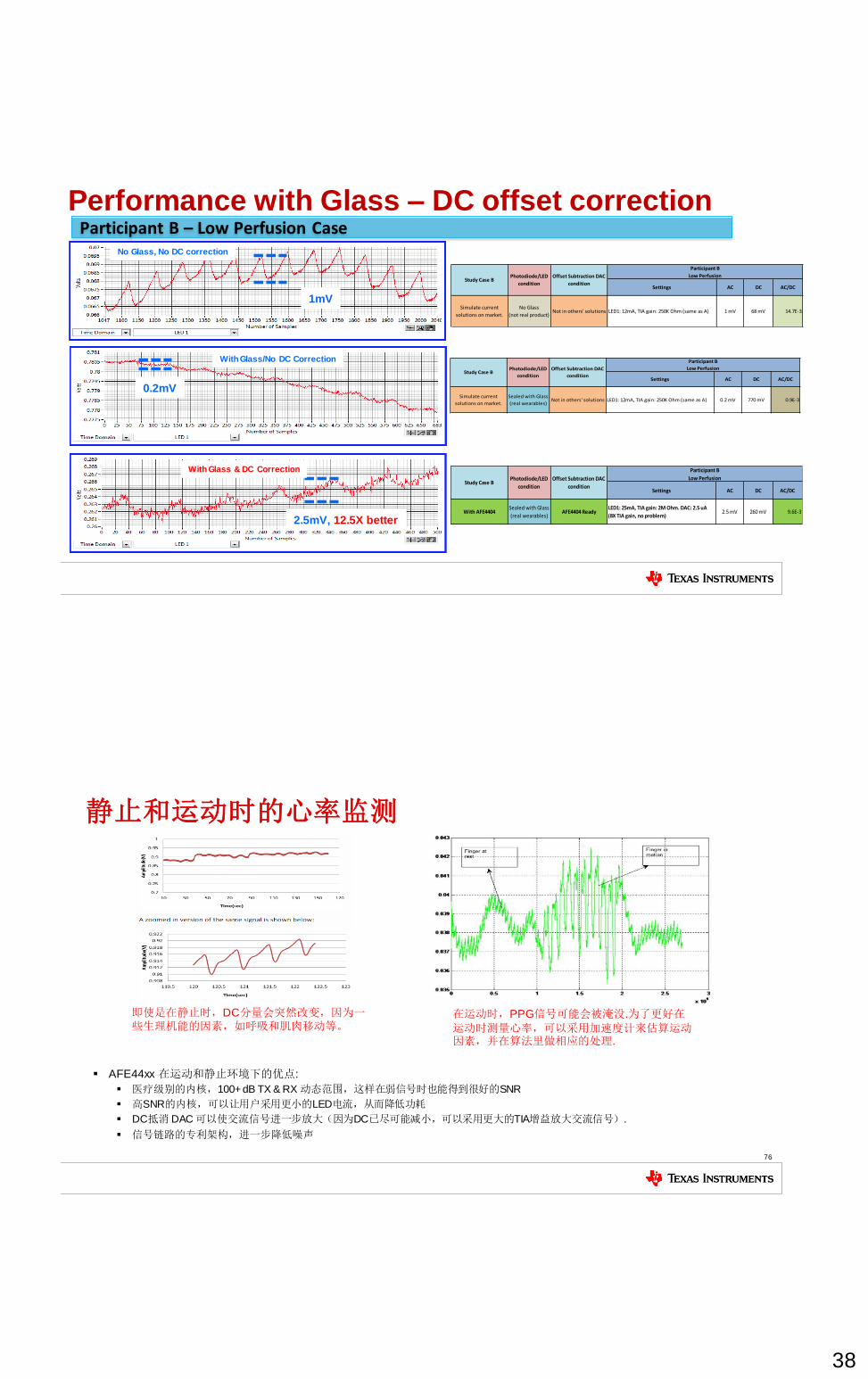
Performance with Glass – DC offset correction Participant B – Low Perfusion Case
Settings AC DC AC/DC
Simulate current
solutions on market.
Sealed with Glass
(real wearables)Not in others' solutions LED1: 12mA, TIA gain: 250K Ohm (same as A) 0.2 mV 770 mV 0.9E-3
Offset Subtraction DAC
conditionStudy Case B
Participant B
Low PerfusionPhotodiode/LED
condition
1mV
0.2mV
With Glass/No DC Correction
No Glass, No DC correction
Settings AC DC AC/DC
With AFE4404Sealed with Glass
(real wearables)AFE4404 Ready
LED1: 25mA, TIA gain: 2M Ohm. DAC: 2.5 uA
(8X TIA gain, no problem)2.5 mV 260 mV 9.6E-3
Offset Subtraction DAC
conditionStudy Case B
Participant B
Low PerfusionPhotodiode/LED
condition
2.5mV, 12.5X better
With Glass & DC Correction
Settings AC DC AC/DC
Simulate current
solutions on market.
No Glass
(not real product)Not in others' solutions LED1: 12mA, TIA gain: 250K Ohm (same as A) 1 mV 68 mV 14.7E-3
Offset Subtraction DAC
conditionStudy Case B
Participant B
Low PerfusionPhotodiode/LED
condition
静止和运动时的心率监测
AFE44xx 在运动和静止环境下的优点:
医疗级别的内核,100+ dB TX & RX 动态范围,这样在弱信号时也能得到很好的SNR
高SNR的内核,可以让用户采用更小的LED电流,从而降低功耗
DC抵消 DAC 可以使交流信号进一步放大(因为DC已尽可能减小,可以采用更大的TIA增益放大交流信号).
信号链路的专利架构,进一步降低噪声
76
即使是在静止时,DC分量会突然改变,因为一些生理机能的因素,如呼吸和肌肉移动等。
在运动时,PPG信号可能会被淹没.为了更好在运动时测量心率,可以采用加速度计来估算运动因素,并在算法里做相应的处理.
39
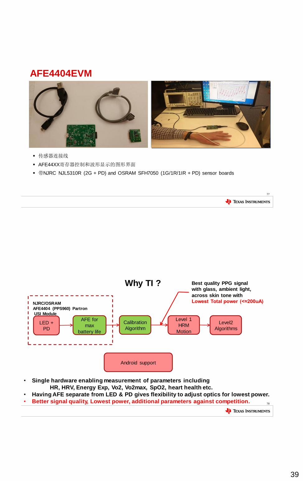
AFE4404EVM
传感器连接线
AFE44XX寄存器控制和波形显示的图形界面
带NJRC NJL5310R (2G + PD) and OSRAM SFH7050 (1G/1R/1IR + PD) sensor boards
77
78
TI Information - NDA
Why TI ?
LED +
PD
AFE for
max
battery life
Calibration
Algorithm
Level 1
HRM
Motion
Level2
Algorithms
Android support
Best quality PPG signal
with glass, ambient light,
across skin tone with
Lowest Total power (<≈200uA) NJRC/OSRAM
AFE4404 (PPS960) Partron
USI Module
• Single hardware enabling measurement of parameters including
HR, HRV, Energy Exp, Vo2, Vo2max, SpO2, heart health etc.
• Having AFE separate from LED & PD gives flexibility to adjust optics for lowest power.
• Better signal quality, Lowest power, additional parameters against competition.
40
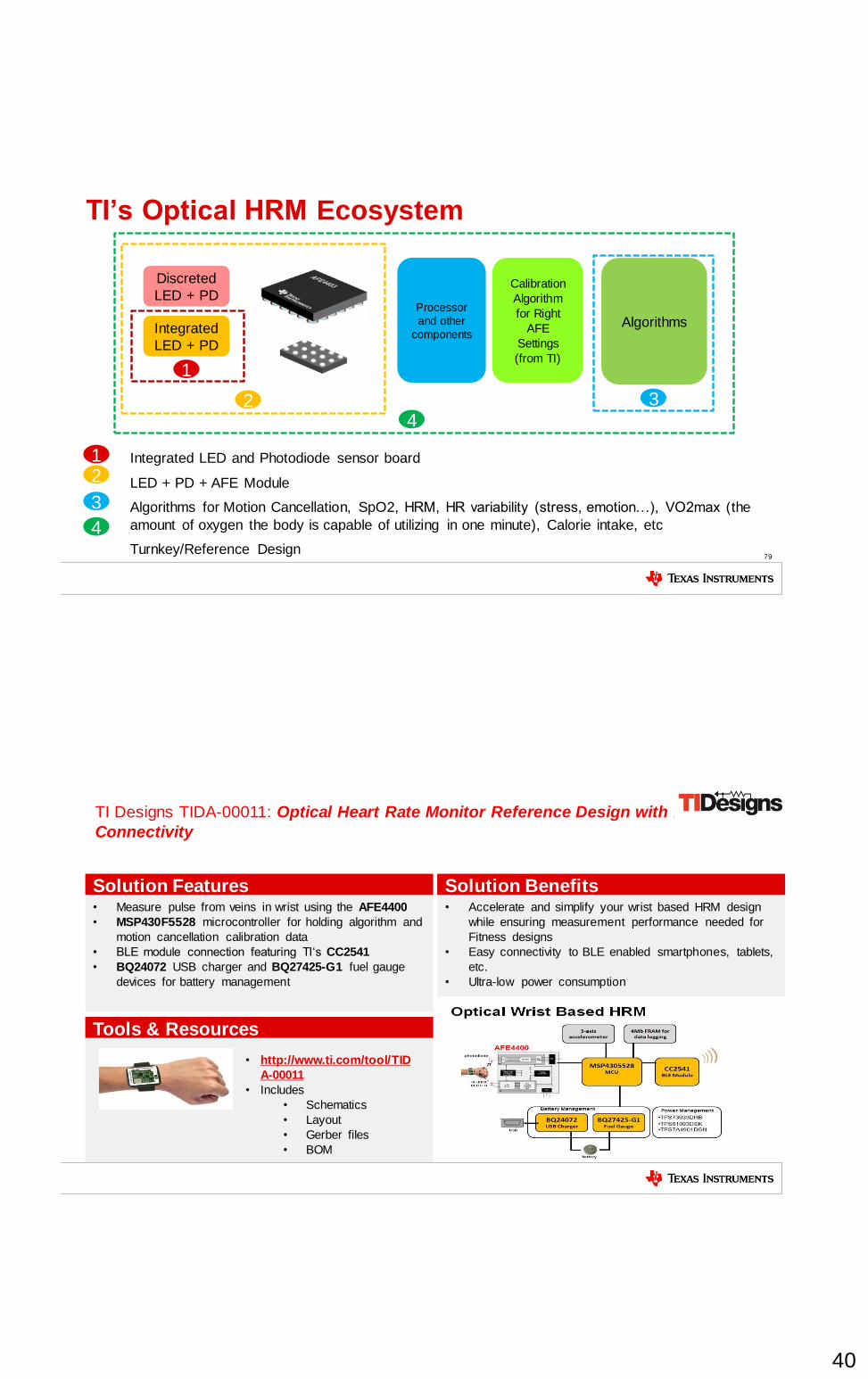
TI’s Optical HRM Ecosystem
Integrated LED and Photodiode sensor board
LED + PD + AFE Module
Algorithms for Motion Cancellation, SpO2, HRM, HR variability (stress, emotion…), VO2max (the
amount of oxygen the body is capable of utilizing in one minute), Calorie intake, etc
Turnkey/Reference Design 79
Discreted
LED + PD
Integrated
LED + PD
Processor
and other
components
Calibration
Algorithm
for Right
AFE
Settings
(from TI)
Algorithms
1
2 3 4
1 2
3
4
• Measure pulse from veins in wrist using the AFE4400
• MSP430F5528 microcontroller for holding algorithm and
motion cancellation calibration data
• BLE module connection featuring TI‘s CC2541
• BQ24072 USB charger and BQ27425-G1 fuel gauge
devices for battery management
• Accelerate and simplify your wrist based HRM design
while ensuring measurement performance needed for
Fitness designs
• Easy connectivity to BLE enabled smartphones, tablets,
etc.
• Ultra-low power consumption
Solution Features
TI Designs TIDA-00011: Optical Heart Rate Monitor Reference Design with BLE
Connectivity
Solution Benefits
Tools & Resources
• http://www.ti.com/tool/TID
A-00011
• Includes
• Schematics
• Layout
• Gerber files
• BOM
41
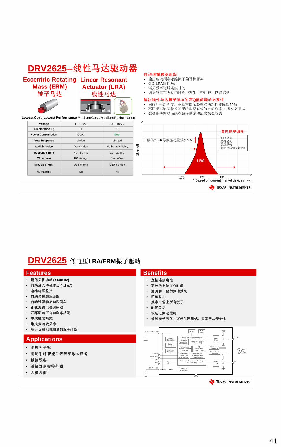
Eccentric Rotating
Mass (ERM)
转子马达
DRV2625--线性马达驱动器
81
Linear Resonant
Actuator (LRA)
线性马达
Voltage 1 – 10 VDC 2.5 – 10 VDC
Acceleration (G) ~1 ~1-2
Power Consumption Good Best
Freq. Response Limited Limited
Audible Noise Very Noisy Moderately Noisy
Response Time 40 – 80 ms 20 – 30 ms
Waveform DC Voltage Sine Wave
Min. Size (mm) Ø5 x 8 long Ø10 x 3 high
HD Haptics No No
* Based on current market devices
Lowest Cost, Lowest Performance Medium Cost, Medium Performance
Frequency (Hz)
Str
ength
LRA
170 180 175
频偏2.5Hz导致振动量减少40% 制造误差 器件老化 温度影响 固定方法和安装位置
81
谐振频率偏移
自动谐振频率追踪
• 输出驱动频率跟踪振子的谐振频率
• 针对LRA线性马达
• 谐振频率追踪是实时的
• 谐振频率在振动的过程中发生了变化也可以追踪到
解决线性马达振子频响的高Q值问题的必要性
• 同样的振动强度,驱动在谐振频率点的功耗能降低50%
• 不用频率追踪技术就无法实现有效的启动和停止!振动效果差
• 驱动频率偏移谐振点会导致振动强度快速减弱
• 手机和平板
• 运动手环智能手表等穿戴式设备
• 触控设备
• 遥控器鼠标等外设
• 人机界面
• 直接连接电池
• 更长的电池工作时间
• 清脆和一致的振动效果
• 简单易用
• 兼容市场上所有振子
• 配置灵活
• 低延迟振动控制
• 检测振子失效,方便生产测试,提高产品安全性
DRV2625 低电压LRA/ERM振子驱动
• 超低关机功耗 (< 500 nA)
• 自动进入待机模式 (< 2 uA)
• 电池电压监控
• 自动谐振频率追踪
• 自动过驱动启动和刹车
• 正弦波输出失谐驱动
• 开环驱动下自动刹车功能
• 单线触发模式
• 集成振动效果库
• 基于负载阻抗测量的振子诊断
Features Benefits
Applications
I2C
I/F
REG
Back-EMF
Detection
Control and Playback Engine
MLRA
or
ERM
OUT–
GND
REG
TRIG/INTZ
SDA
SCL
NRST
Brownout
Protection
Supply
Correction
Automatic
Over-Drive
and Braking
Gate
Drive
VDD
Automatic Resonance Tracking
and Reporting
Waveform Shape
Select (LRA)
Gate
Drive
VDD
OUT+
VDD ROMReg
Map2.7 V – 5.5 V
1.8 V
Loopable
Waveform
Sequencer
Dynamic and
Programmable
Output Clamp
Impedance
Based Actuator
DiagnosticsShort Circuit
Protection
Off-
Resonance
Driving (LRA)
Thermal
Protection
Battery
Monitor
42
Applications
Features Benefits
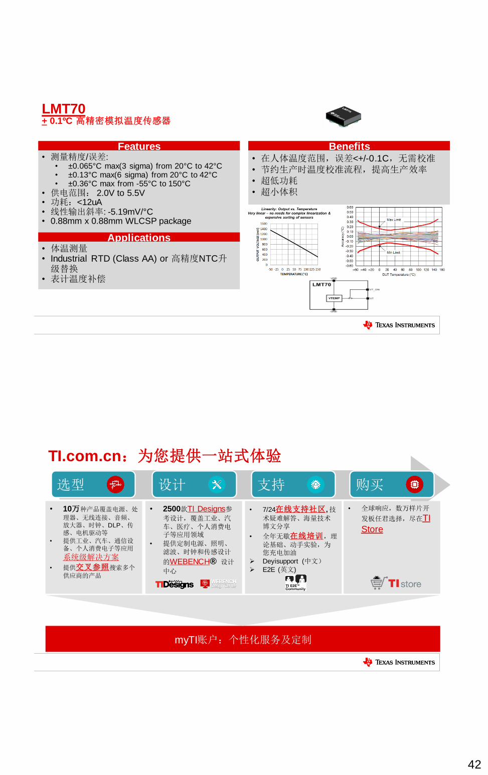
LMT70 + 0.1ºC 高精密模拟温度传感器
• 测量精度/误差: • ±0.065°C max(3 sigma) from 20°C to 42°C • ±0.13°C max(6 sigma) from 20°C to 42°C • ±0.36°C max from -55°C to 150°C
• 供电范围: 2.0V to 5.5V • 功耗:<12uA • 线性输出斜率: -5.19mV/°C • 0.88mm x 0.88mm WLCSP package
• 体温测量 • Industrial RTD (Class AA) or 高精度NTC升级替换
• 表计温度补偿
• 在人体温度范围,误差<+/-0.1C,无需校准
• 节约生产时温度校准流程,提高生产效率
• 超低功耗
• 超小体积
84
选型 设计 支持 购买
• 10万种产品覆盖电源、处
理器、无线连接、音频、放大器、时钟、DLP、传感、电机驱动等
• 提供工业、汽车、通信设备、个人消费电子等应用
系统级解决方案
• 提供交叉参照搜索多个
供应商的产品
TI.com.cn:为您提供一站式体验
• 全球响应,数万样片开
发板任君选择,尽在TI
Store
myTI账户:个性化服务及定制
• 7/24在线支持社区, 技
术疑难解答、海量技术博文分享
• 全年无歇在线培训,理论基础、动手实验,为您充电加油
Deyisupport (中文)
E2E (英文)
• 2500款TI Designs参考设计,覆盖工业、汽车、医疗、个人消费电子等应用领域
• 提供定制电源、照明、滤波、时钟和传感设计
的WEBENCH® 设计
中心
43
myTI 账户: 专属您的私人订制
85
https://my.ti.com 加入myTI 会员的好处: • TIstore 一站式购物平台, 数万样片
开发工具,一网打尽
• 参与 TI 在线技术支持社区
• 利用 WEBENCH® 设计工具轻松进行设计
和模拟
• 订阅产品更新,获得最新设计工具,
系统方框图与指南等信息
• 标记您最喜爱的产品
• 管理 / 订阅新闻简报
• 注册 / 参加在线培训与活动
• 获得个性化的建议
TI 在线培训: 打破时空,随手可得
• 提供包括从理论基础到深入的动手实验在内的各种在线和现场的培训,协助您将新一代的设计化为现实。我们整合式的培训项目包括
1000+ 的线上培训课程,网络研讨会和线下研讨会,有助于您使用TI产品,开发工具,软件和各类应用设计。
86
经典热门课程:
• C2837x 入门指南
• 2016 EP 研讨会线下课程
• 2016 工业研讨会
• 高精度实验室
• BMS电池设计探讨
• WEBENCH 系列课程
• Engineer It 系列课程
http://www.ti.com.cn/training
IMPORTANT NOTICE有有关关 TI 设设计计信信息息和和资资源源的的重重要要通通知知
德州仪器 (TI) 公司提供的技术、应用或其他设计建议、服务或信息,包括但不限于与评估模块有关的参考设计和材料(总称“TI 资源”),旨在帮助设计人员开发整合了 TI 产品的 应用; 如果您(个人,或如果是代表贵公司,则为贵公司)以任何方式下载、访问或使用了任何特定的TI 资源,即表示贵方同意仅为该等目标,按照本通知的条款进行使用。TI 所提供的 TI 资源,并未扩大或以其他方式修改 TI 对 TI 产品的公开适用的质保及质保免责声明;也未导致 TI 承担任何额外的义务或责任。TI 有权对其 TI 资源进行纠正、增强、改进和其他修改。您理解并同意,在设计应用时应自行实施独立的分析、评价和 判断, 且应全权负责并确保 应用的安全性, 以及您的 应用 (包括应用中使用的所有 TI 产品))应符合所有适用的法律法规及其他相关要求。你就您的 应用声明,您具备制订和实施下列保障措施所需的一切必要专业知识,能够 (1) 预见故障的危险后果,(2) 监视故障及其后果,以及 (3) 降低可能导致危险的故障几率并采取适当措施。您同意,在使用或分发包含 TI 产品的任何 应用前, 您将彻底测试该等 应用 和该等应用所用 TI 产品的 功能。除特定 TI 资源的公开文档中明确列出的测试外,TI 未进行任何其他测试。您只有在为开发包含该等 TI 资源所列 TI 产品的 应用时, 才被授权使用、复制和修改任何相关单项 TI 资源。但并未依据禁止反言原则或其他法理授予您任何TI知识产权的任何其他明示或默示的许可,也未授予您 TI 或第三方的任何技术或知识产权的许可,该等产权包括但不限于任何专利权、版权、屏蔽作品权或与使用TI产品或服务的任何整合、机器制作、流程相关的其他知识产权。涉及或参考了第三方产品或服务的信息不构成使用此类产品或服务的许可或与其相关的保证或认可。使用 TI 资源可能需要您向第三方获得对该等第三方专利或其他知识产权的许可。TI 资源系“按原样”提供。TI 兹免除对 TI 资源及其使用作出所有其他明确或默认的保证或陈述,包括但不限于对准确性或完整性、产权保证、无屡发故障保证,以及适销性、适合特定用途和不侵犯任何第三方知识产权的任何默认保证。TI 不负责任何申索,包括但不限于因组合产品所致或与之有关的申索,也不为您辩护或赔偿,即使该等产品组合已列于 TI 资源或其他地方。对因 TI 资源或其使用引起或与之有关的任何实际的、直接的、特殊的、附带的、间接的、惩罚性的、偶发的、从属或惩戒性损害赔偿,不管TI 是否获悉可能会产生上述损害赔偿,TI 概不负责。您同意向 TI 及其代表全额赔偿因您不遵守本通知条款和条件而引起的任何损害、费用、损失和/或责任。本通知适用于 TI 资源。另有其他条款适用于某些类型的材料、TI 产品和服务的使用和采购。这些条款包括但不限于适用于 TI 的半导体产品(http://www.ti.com/sc/docs/stdterms.htm)、评估模块和样品 (http://www.ti.com/sc/docs/sampterms.htm) 的标准条款。
邮寄地址:上海市浦东新区世纪大道 1568 号中建大厦 32 楼,邮政编码:200122Copyright © 2017 德州仪器半导体技术(上海)有限公司