Embed Size (px)
Citation preview
Timing Error Analysis in Digital-to-Analog Converters- Effects of Sampling Clock Jitter and Timing Skew (Glitch) -
Shinya Kawakami, Haruo Kobayashi, Naoki Kurosawa, Ikkou Miyauchi,Hideyuki Kogure, Takanori Komuro, Hiroshi Sakayori
Dept. of Electronic Engineering, Gunma University, 1-5-1 Tenjin-cho Kiryu 376-8515 JapanTel: 81-277-30-1788 Fax: 81-277-30-1707 e-mail: k [email protected]
AbstractThis paper describes two timing nonideality issues of Digital-to-Analog Converters(DACs); sampling clock jitter and clock skew effects. (i) A formula for the outputerror power due to sampling clock jitter is derived, and this has been validatedby numerical simulation; spectrum characteristics of jitter-related noise are alsoexamined. We have also found that when an analog lowpass filter follows the DACand only the noise power inside the signal band is considered, increasing jitter andincreasing input signal frequency degrade the DAC SNR. (ii) The clock timing skewinside the DAC causes glitch impulses. We try to characterize them by simulationand we have found the followings; as the input frequency increases, the effects ofthe glitch on the DAC SNR decrease. The effects of the glitch due to upper bits onthe DAC SNR and SFDR are more significant than due to lower bits. Also glitchpower is mainly located at the odd-multiple frequencies of the input signal.Keywords: DAC, Sampling, Jitter, Clock Skew, Glitch
1 Introduction
Digital-to-Analog Converters (DACs) are essential components in communication systems(such as transceivers) and measuring instruments (such as arbitrary waveform signal gen-erators), and higher sampling speed is being demanded of them [1, 2, 3]. For such DACswith high sampling speed, the effects of timing error may be crucial, and in this paper wehave investigated two timing error issues: sampling clock jitter and clock timing skew in-side the DAC. These nonidealities of DACs have not been well characterized even thoughthose of Analog-to-Digital Converters (ADCs) and sampling circuits have been [5, 6]. Inthis paper we analyze these effects in theory and by numerical simulation.
2 Sampling Clock Jitter Effects
2.1 DAC Output Error Power due to Sampling Clock Jitter
A. Problem Formulation : Fig.1 shows a DAC with a digital input Vin(n) applied, andsampling clock is CLK. Ideally the sampling clock CLK operates with a period of Ts forevery cycle, however in reality its timing can fluctuate which is called clock jitter or phasenoise (Fig.2) [7]. If we denote clock jitter as εn, then the n-th sampling timing of CLK isnTs + εn instead of nTs. Since the jitter εn is sufficiently smaller than the sampling periodof Ts in most practical situations, we assume that
−Ts
2< εn <
Ts
2. (1)
Also we assume that the DAC has sufficiently good resolution that quantization can beneglected, and that the DAC output Vout(t) is zero-order hold [3]. Then Fig.3 shows theDAC outputs with an ideal clock (no jitter) and with a real clock (with jitter) while Fig.4shows the DAC output error due to clock jitter.
1

B. Formula for Error Power due to Jitter : The DAC output error power Pe due tothe sampling clock jitter is defined as follows:
Pe := limN→∞
1
N
N−1∑n=0
e2n|εn| (2)
Here en is the DAC output error due to jitter (see Fig.4). If the input signal Vin(t) and thesampling jitter are not correlated (which is the case in general), εn and en are independentand we obtain
Pe = E[e2n]E[|εn|]. (3)
Proposition : When the input Vin(n) to the DAC is a cosine wave Vin(n) = A cos(2π fin
fsn),
the error power Pe due to jitter is given by
Pe = 2A2 sin2(πfin
fsn)E[|ε|].
Here fin is the input frequency and fs is the sampling frequency (fs = 1/Ts).
Proof of Proposition : See [8].We remark that references [9, 10] discuss nonuniform sampling effects in DACs. However,our problem formulation is different from theirs.
2.2 Numerical Simulation of DAC Output Error Power due to SamplingClock Jitter
Example 1 : Suppose that the jitter εn follows a uniform distribution whose probabilityfunction p(εn) is as shown in Fig. 5:
p(εn)=
{12a
(−a ≤ εn ≤ a, where 0 < a < Ts/2)0 (otherwise).
Note that 0 < a < Ts/2 according to eq.(1). Since E[|εn|] = a/2, we obtain
Pe = A2a sin2(πfin
fs). (4)
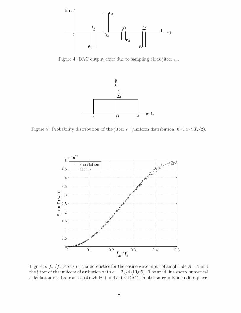
Fig.6 shows a graph of fin/fs versus Pe calculated numerically from eq.(4) and a graphobtained from a DAC simulation including jitter, where a = Ts/4 and A = 2 are used inboth cases. We see that both match well.
Example 2 : Suppose that the jitter εn follows a distribution whose probability functionis of cosine-squared shape as shown in Fig.7:
p(εn)=
{1acos2(πεn
2a) (−a ≤ εn ≤ a, 0 < a < Ts/2)
0 (otherwise).
Since E[|εn|] = a(π2 − 4)/(2π2), we obtain
Pe =1
π2(π2 − 4)A2a2 sin2(π
fin
fs
). (5)
Fig.8 shows a graph of fin/fs versus Pe calculated numerically from eq.(5) and a graphobtained from a DAC simulation including jitter, with a = Ts/4 and A = 2 in both cases.We see that both match well.Remark In general, quantization noise (which we neglected in our problem formulation),and the noise due to the sampling jitter in a DAC, are statistically independent. Hencethe total error power when both the quantization and the sampling jitter exist is just thesimple sum of the error power due to quantization and that due to sampling jitter.
2

2.3 Power Spectrum of DAC Output Error due to Sampling Clock Jitter
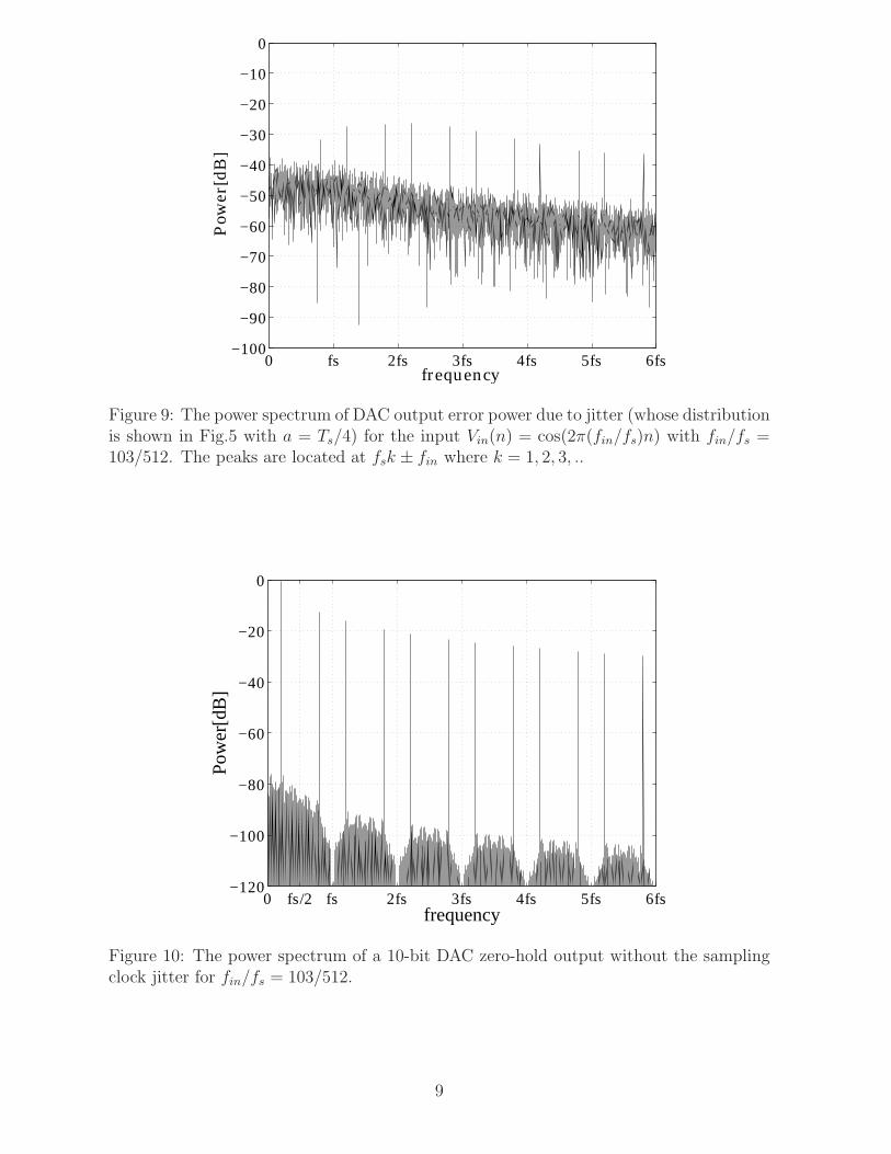
Next we consider the power spectrum characteristics of the DAC output error due to jitter.Suppose that the input Vin(n) to the DAC is a cosine wave Vin(n) = A cos(2π(fin/fs)n)and the DAC suffers from uniformly-distributed sampling clock jitter (Fig.5). Fig.9 showssimulation results of the power spectrum of the error, and we see that their power haspeaks at
kfs ± fin (k = 1, 2, 3, ...). (6)
2.4 Sampling Jitter Effects on DAC SNR
In this section we show that the sampling clock is very serious by analyzing their effects onDAC SNR. Fig.10 shows the power spectrum of a 10-bit ideal DAC output without jitterfor fin/fs = 103/512, 2048. Note that the DAC output error due to the zero-order holdoutput has power spectrum peaks at kfs±fin (k = 1, 2, 3, ...) [3], and it follows from eq.(6)that the DAC output errors due to jitter and zero-order hold have power spectrum peaksat the same frequencies. On the other hand, Fig.11 shows the power spectrum of the sameDAC with jitter (cosine-squared distribution of a = Ts/4 in Fig.7), and we see that thenoise floor increases. Figs.12 and 13 show the SNRs of the DAC with and without jitter,where the total noise (outside as well as inside the signal band) is considered. We see thatSNR degrades slightly (by a few dB). However, in practical situations, the DAC is oftenfollowed by an analog low-pass filter which sufficiently attenuates the noise componentsbeyond fs/2. In this case we consider that SNR is given by
10log10 {signal power}/ {noise power between 0 to fs/2 (total noise power in the signalband)} [dB].Figs.14 and 15 show that the DAC SNR using the above definition degrades significantlydue to the sampling jitter, and these results can be interpreted as follows; the noise powerdue to the zero-hold output and jitter has peaks at kfs ± fin (k = 1, 2, 3, ...) (which ishigher than fs/2 for all k). Thus if we consider the whole noise, the dominant noise peaksare located at these frequencies. The sampling clock jitter induces spread spectrum effectsfor these frequency noise peaks (as well as the signal power peak) and the power at thesefrequencies is widely spread out to other frequencies, and hence the noise floor increases.However, the total noise power remains almost constant. Hence, when the total noisepower is considered, the DAC SNR is almost constant regardless of sampling jitter. Onthe other hand, when only the noise inside the signal band fs/2 is taken into account, theSNR degrades significantly because the noise floor inside the signal band is raised by thejitter.
3 Clock Timing Skew Effects
3.1 Glitch and Clock Timing Skew
Glitch is one of the important performance specification of DACs [3], and it is caused bythe clock timing skew inside the DAC. Consider a binary-weighted current steering DACin Fig.16, where the digital input changes from code 7 to code 8. When the digital inputis 7, switches D3, D2 and D1 are ON and the output voltage is 7IR. When the digitaloutput is 8, switches D4 is ON and the output voltage is 8RI. Suppose that during theinput transition from 7 to 8, the the switch D4 turns on slightly before the switches D1,D2 and D3 turn off; in a transition moment, all of the switches D1, D2, D3 and D4 areON, which outputs an impulse voltage of 15IR, and this is called ”glitch”. The switchtiming difference among D1, D2, D3 and D4 are caused by the skew among the clocksinside the DAC which control on and off of the current switches. The glitch degradesSNR and SFDR of the DAC, and also an amplifier circuit following the DAC often can
3

not respond to the impulse. Note that this glitch impulse is caused and problematic evenwhen the input frequency is low. To our knowledge, the glitch characteristics itself hasnot been well-investigated theoretically, and in this paper we will try to clarify it. Onthe other hand, several DAC architecture and circuit techniques have been proposed toreduce the glitch as follows:(i) In many high-speed DACs, segmented configuration for the upper bits is used for theglitch reduction while binary-weighted configuration for the lower bits is used for thehardware and power reduction [4].(ii) A track-and-hold (T/H) circuit sometimes follows the DAC output for the glitch effectreduction, and such a T/H circuit is called as ”deglitcher circuit” [4]. However it is verydifficult to design such a T/H circuit to meet the specification requirements of very highperformance DACs.(iii) Recently a track-and-attenuation (T/A) circuit is proposed to replace the T/H circuitas a deglitcher [11]. The T/A circuit is relatively easy to design though it reduces thesignal power of the DAC output by a factor of 2.(iv) Note that in principle the glitch can not be reduced even if the differential output isused [4].
3.2 Glitch Simulation
We have simulated the DAC glitch effects using C programs. In the simulation, weassume that the DAC employs an 8-bit binary-weighted current steering architecture andits output is zero-hold. The DAC output is analog and it is continuous in time, and hencefor our digital simulation we have “subsampled” the sampling period Ts by a factor ofM (here M = 64). In our simulation, the data of N sampling prediods (here N = 128)were collected and hence we have performed N × M-point discrete Fourier transform toobtain the DAC output power spectrum. Figs.17-20 show the simulation results of theDAC output waveforms and its power spectrum with some timing skews. Fig.21 showsthe simulation results for the DAC SNR versus timing skew.
From these results, we have obtained the following observations:(i) Effects of the glitch due to upper bits on the DAC SNR and SFDR are more significantthan due to lower bits.(ii) As the timing skew increases, its effects on the DAC SNR and SFDR become moreserious.(iii) As the input frequency increases, the effects of the glitch on the DAC SNR decreases.(iv) The glitch power spectrum has peaks at odd-multiple frequencies of fin and it doesnot have much power at its even-multiples. This corresponding the fact that “the glitchcan not be reduced even if the differential output is used”.Remark However, in our experiences, the glitch power spectrum of actual DACs oftenhas a finite (nonzero) value at even-multiples of fin as well as its odd-multiples; this wouldbe probably because the propagation delay time of tpdON for a current switch to turn onand that of tpdOFF to turn off are different. We are trying to incorporate this effect in oursimulation.
4 Concluding Remarks
As an on-going project, we are investigating the following:(i) Quantitative analysis of the glitch in the segmented (for upper bits) + binary-weighted(for lower bits) DAC architecture, as well as in the binary-weighted (for all bits) DACarchitecture.(ii) Quantitative clarification of the relationships between the input frequency and theglitch energy.
4

(iii) Confirmation of the results here by SPICE simulation.By considering the timing error analysis in this paper, we have desinged and laid-out
a 10bit CMOS DAC and it is now under fabrication (Figs.22, 23, 24), and its designcontents may be also reported at the conference.
Acknowledgements
We would like to thank H. Okano, M. Iwasaki and K. Wilkinson for valuable discussions.
References
[1] H. Kobayashi, K. Kobayashi, H. Sakayori and Y. Kimura, “ADC Standard and Test-ing in Japanese Industry”, Computer Standards & Interfaces, Elsevier Publishers,vol.23, pp.57-64 (March 2001).
[2] M. Gustavsson, J. J. Wikner and N. N. Tan, CMOS Data Converters for Communi-cations, Kluwer Academic Publihsers (2000).
[3] B. Razavi, Principles of Data Conversion System Design, IEEE Press (1995).
[4] R. Plasshce, Integrated Analog-to-Digital and Digital-to-Analog Converters, KluwerAcademic Publishers (1994).
[5] H. Kobayashi, K. Kobayashi, M. Morimura, Y. Onaya, Y. Takahashi, K. Enomoto,and H. Kogure, “Sampling Jitter and Finite Aperture Time Effects in WidebandData Acquisition Systems,” IEICE Trans. on Fundamentals, vol. E85-A, no. 2 (Feb.2002).
[6] M. Shinagawa, Y. Akazawa and T. Wakimoto, “Jitter Analysis of High-Speed Sam-pling Systems,” IEEE J. of Solid-State Circuits, vol.25, no.1, pp.220-224 (Feb. 1990).
[7] A. Hajimiri and T. Lee, “A General Theory of Phase Noise in Electrical Oscillators,”IEEE J. of Solid-State Circuits, vol.33, no.2, pp.179-193 (Feb. 1998).
[8] N. Kurosawa, H. Kobayashi, H. Kogure, T. Komuro and H. Sakayori, ”SamplingClock Jitter Effects in Digital-to-Analog Converters,” Measurement, Journal of theInternational Measurement Confederation IMEKO, Special Issue on DAC Modellingand Testing, vol.31, no.3, pp.187-199 (March 2002).
[9] Y.-C. Jenq, “Digital-to-Analog (D/A) Converters with Nonuniformly Sampled Sig-nals,” IEEE Trans. on Instrumentation and Measurement, vol.45, no.1, pp.56-59(June 1997).
[10] Y.-C. Jenq, “Direct Digital Synthesizer with Jittered Clock,” IEEE Trans. on In-strumentation and Measurement, vol.46, no.3, pp.653-655 (Feb. 1996).
[11] A. R. Bugeja and B.-S. Song, “A Self-Trimming 14b 100MSample/s CMOS DAC,”IEEE J. of Solid-State Circuits, vol.35, no.12, pp.1841-1852 (Dec. 2000).
5

DAC
CLK
Digital Analog
Vin(n) Vout(t)
Figure 1: A DAC with digital input signal, sampling clock and analog output signal.
Ts/2 Ts/2
εn
ideal CLK
CLK with jitter
Figure 2: Ideal sampling clock (without jitter) and actual sampling clock (with jitter εn)provided to a DAC.
0 tT 2T 3T 4T 5Ts s s s s
e
ee
e
ε
ε ε
ε
1
1
2
2
3
3
4
4Vout(t)
w/o jitterw/ jitter
CLK
Figure 3: DAC output waveforms with ideal sampling clock (without jitter) and actualsampling clock (with jitter εn).
6
0 t
e
e
ee
ε
ε
ε ε1
1
2
2
3
3
4
4
Error
Figure 4: DAC output error due to sampling clock jitter εn.
p
0 a-a
2a1
εn
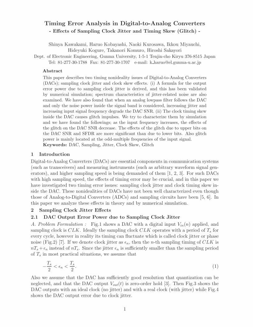
Figure 5: Probability distribution of the jitter εn (uniform distribution, 0 < a < Ts/2).
0 0.1 0.2 0.3 0.4 0.50
0.5
1
1.5
2
2.5
3
3.5
4
4.5
5x 10
−4
fin
/ fs
Err
or P
ower
simulationtheory
Figure 6: fin/fs versus Pe characteristics for the cosine wave input of amplitude A = 2 andthe jitter of the uniform distribution with a = Ts/4 (Fig.5). The solid line shows numericalcalculation results from eq.(4) while + indicates DAC simulation results including jitter.
7

p
0 a-a
a1
εn
Figure 7: Probability distribution of the jitter εn (cosine squared distribution, 0 < a <Ts/2).
0 0.1 0.2 0.3 0.4 0.50
0.5
1
1.5
2
2.5
3x 10
−4
fin
/ fs
Err
or P
ower
simulationtheory
Figure 8: fin/fs versus Pe characteristics for the cosine wave input of amplitude A = 2and the jitter of the cosine squared distribution (Fig.7) with a = Ts/4. The solid lineshowsnumerical calculation results from eq.(5) while + indicates DAC simulation resultsincluding jitter.
8
0 fs 2fs 3fs 4fs 5fs 6fs−100
−90
−80
−70
−60
−50
−40
−30
−20
−10
0
frequency
Pow
er[d
B]
Figure 9: The power spectrum of DAC output error power due to jitter (whose distributionis shown in Fig.5 with a = Ts/4) for the input Vin(n) = cos(2π(fin/fs)n) with fin/fs =103/512. The peaks are located at fsk ± fin where k = 1, 2, 3, ..
0 fs/2 fs 2fs 3fs 4fs 5fs 6fs−120
−100
−80
−60
−40
−20
0
frequency
Pow
er[d
B]
Figure 10: The power spectrum of a 10-bit DAC zero-hold output without the samplingclock jitter for fin/fs = 103/512.
9

0 fs/2 fs 2fs 3fs 4fs 5fs 6fs−120
−100
−80
−60
−40
−20
0
frequency
Pow
er[d
B]
Figure 11: The power spectrum of a 10-bit DAC zero-hold output with the sampling clockjitter of cosine squared distribution of a = Ts/4 (Fig.7), for fin/fs = 103/512.
0 0.1 0.2 0.3 0.4 0.5−10
0
10
20
30
40
50
fin
/ fs
SN
R[d
B]
w/o jitterw/ jitter
Figure 12: Simulation result of SNR versus fin/fs of a 10-bit DAC with and without jitterof cosine squared distribution of a = Ts/4 (Fig.7). Here the total noise power outside aswell as inside the signal band is considered.
10

0 0.1 0.2 0.3 0.4 0.538
38.5
39
39.5
a / Ts
SN
R[d
B]
Figure 13: Simulation result of SNR versus the jitter a/Ts of a 10-bit DAC with jitter ofcosine squared distribution (Fig.7) for fin/fs = 3/512. Here the total noise power outsideas well as inside the signal band is considered.
0 0.1 0.2 0.3 0.4 0.510
20
30
40
50
60
70
fin
/ fs
SN
R[d
B] w/o jitter
w/ jitter
Figure 14: Simulation result of SNR versus fin/fs of a 10-bit DAC with and without jitterof cosine squared distribution of a = Ts/4 (Fig.7). Here only the noise power inside thesignal band fs/2 is considered.
11

0 0.1 0.2 0.3 0.4 0.540
45
50
55
60
65
a / Ts
SN
R[d
B]
Figure 15: Simulation result of SNR versus the jitter a/T of a 10-bit DAC with jitter ofcosine squared distribution (Fig.7) for fin/fs = 3/512. Here only the noise power insidethe signal band fs/2 is considered.
glitch
w/o timing skew w/ timing skew
Figure 16: Glitch causing mechanism in a current steering DAC. Suppose that the switchD4 turns on before the other switches turn off (due to clock timing skew) when the inputchanges from code 7 to code 8. Then a glitch impulse of 15IR is caused during thetransition.
12

Output waveform
DAC Output Power Spectrum
time
Sig
nal l
evel
Pow
er[d
B]
frequency
Ts/2
(b)
(a)
fin 3fin5fin
7fin9fin
SFDR=16.58[dB]
Figure 17: Simulation results for a sinusoidal input in case that the switch for MSB(D8) changes faster by Ts/2 than those for the other bits. (a) DAC output waveform forfin = fs/128. (b) DAC output power spectrum for fin = (11/128)fs.
Output waveform
DAC Output Power Spectrum
time
Sig
nal l
evel
Pow
er[d
B]
frequency
Ts /2
(b)
(a)
fin 3fin
5fin7fin 9fin
SFDR=25.99[dB]
Figure 18: Simulation results for a sinusoidal input in case that the switch for MSB-2(D6) changes faster by Ts/2 than those for the other bits. (a) DAC output waveform forfin = fs/128. (b) DAC output power spectrum for fin = (11/128)fs.
13

Output waveform
DAC Output Power Spectrumtime
Sig
nal l
evel
Pow
er[d
B]
frequency
Ts /2
(b)
(a)
fin
SFDR=36.54[dB]
Figure 19: Simulation results for a sinusoidal input in case that the switch for MSB-4(D4) changes faster by Ts/2 than those for the other bits. (a) DAC output waveform forfin = fs/128. (b) DAC output power spectrum for fin = (11/128)fs.
Output waveform
DAC Output Power Spectrum
time
Sig
nal l
evel
Pow
er[d
B]
frequency
Ts /2
(b)
(a)
fin
SFDR=45.81[dB]
Figure 20: Simulation results for a sinusoidal input in case that the switch for LSB (D1)changes faster by Ts/2 than those for the other bits. (a) DAC output waveform forfin = fs/128. (b) DAC output power spectrum for fin = (11/128)fs.
14

- Ts2
Ts2
timing skew
(a) D8 case.
(b) D4 case.
(c) D1 case.
fin /fs= 1/128
fin /fs=11/128
fin /fs=31/128
Figure 21: Timing skew (of D8, D4, D1) versus SNR for fin/fs = 1/128, 11/128 and31/128.
15

R-2R binary-weighted for lower 6bits
Segmented structurefor higher bits
Figure 22: Analog part of our designed 10bit CMOS DAC, where segmented structure(for higher bits) + R-2R binary-weighted strucuture (for lower bits) is used.
16

Figure 23: Floor plan of our designed 10bit CMOS DAC.
17

Figure 24: Layout of our designed 10bit CMOS DAC, whose die size is 2.6mm x 2.6mmin 1.2µm CMOS process.
18