Embed Size (px)
Citation preview

放射光X線光電子分光法の紹介とpoly-Si/HfAlO界面およびpoly-Si/HfSiON界
面の反応解析への適応池永 英司
JASRI/SPring-8
アウトライン
I. 硬X線励起光電子分光 (HX-PES)利用のこれまでの背景II. HX-PESの紹介と物質科学への応用III. 研究計画

Background1974 First feasibility test of HX-PES @ 8 keV by Lindau et al.
Au 4f: OK, Au valence: impossible, Nature 250, 214 (1974)
2000 Importance of bulk probe was clearly shown by Sekiyama et al.VB spectra of Ce compounds at 880 eV, Nature 430, 396 (2000)
No successful report on HX-VB-PES even after 3rd
generation SR
2001 Preparation of HX-PES started @ SPring-8 (with Kobayashi & Ishikawa)
2002 First feasibility test at BL29XU in SPring-8 @ 6 keVJune large probing depth
surface insensitivityhigh energy resolutionhigh throughput
confirmed for core level and valence band

Sekiyama et al., Nature 430, 396 (2000)
Probing depth @ 1keV: 1~4nmstill surface sensitive!
Inevitable requirement on surface preparation & UHV!
Many inaccessible targets remains!・Thin films・Embedded interface・Multilayer

CollaboratorsJASRI/SPring-8
K. Kobayashi, M. YabashiRIKEN/SPring-8 (Coherent X-ray Optics Lab.)
T. Ishikawa, K. Tamasaku, Y. Nishino, D. MiwaRIKEN/SPring-8 (Soft X-ray Spectroscopy Lab.)
S. Shin, Y. Takata, A. Chainani, K. Horiba, N. Kamakura, T. TokushimaHiSOR, Hiroshima Univ.
M. Taniguchi, H. Namatame, M. Arita, K. ShimadaGAMMADATA SCIENTA
ApplicationMusashi Inst. Technology
T. Hattori, H. Nohira (Si –ULSI gate insulators)Tohoku Univ.
T. Yao, J. J. Kim, H. Makino (Diluted Magnetic Semiconductors)Kochi Univ. Tech.
T. Yamamoto (Theoretical Calc.)JAIST
H. Hori, Y. Yamamoto (Au nano particles)Osaka Univ.
T. Kawai, H. Tanaka (LBMO thin film)

硬X線励起光電子分光 (HX-PES)の紹介と物質科学への応用

Characteristics of HX-PESLarge probing depth!
IMFPs1~4nm @ 1 keV4~15nm @ 6 keV
Inelastic Mean Free Path (IMFP) of Electron(From NIST Data Base)
0 2000 4000 6000 8000 100000
50
100
150
200
250
Si
NaCl
SiO2
GaAs
Au
Electron Kinetic Energy (eV)
Inelastic Mean Path (A)
30Å(SiO2)
210Å(SiO2)
140Å(SiO2)
Al KαSurface insensitive (Bulk sensitive)
Free from surface prep.MBE thin film
Chemical depth analysisEmbedded interface(non distractive)

Obstacles to development of HX-PES
0 10 20 30 40 50 60 70 80 901E-8
1E-7
1E-6
1E-5
1E-4
1E-3
0.01
0.1
1
10
Atomic Number
σ abs (Mb/atom) at 1.04 KeV
1s 2s 2p 3s 3p 4s 3d 4p 5s 4d 5p 6s 5d 4f 6p
0 10 20 30 40 50 60 70 80 901E-8
1E-7
1E-6
1E-5
1E-4
1E-3
0.01
0.1
1
10
σ abs (Mb/atom) at 8.05 KeV
Atomic Number
1s 2s 2p 3s 3p 4s 3d 4p 5s 4d 5p 6s 5d 4f 6p
(1)Photoionization Cross Sections
Rapid decrease!about 1/100
1keV
8keV
(2) Lack of an electron analyzerhigh energy resolutionhigh efficiency
Collaboration with Gammadata Scienta Co.
(3) Technical barrier of operationin a X-ray experimental hutch
No problem.
SPring-8

HXHX--PES at BL29XU in SPringPES at BL29XU in SPring--8 (From June 2002)8 (From June 2002)
SPring-8
Undulator(in vacuum)
Double crystalSi 111
Cut-off mirror
Focusing mirror(vertical)
Channel cutSi 333 Sample
Electron analyzerSES2002 (modified)
x-ray from DXM
Si (333) channel-cut monochro.
Ion chamber

Experimental set-up @ BL29 in SPring-8
x-ray
xyzθ-stage
SES-2002(modified)
CCD
CCD
4-axis stage for alignment
hν
Etop view of set-up
Vacuum10-5~10-6 Torr (for R.T.)<10-9 Torr (for L.T.)

Experimental conditions at BL29XU★ in-vacuum planar undulator (horizontal polarization)★ Si (111) DXM & Si (333) channel cut monochromator★ excitation energy: 5.95 keV★ ∆E: 70meV(with focus)★ stability in energy: <50 meV during 1 week★ photon flux: 2x10¹¹ photons/sec @ 100(V)x100(H) µm2
★ analyzer: SES2002 (Gammadata Scienta), K.E.< 6keVNew analyzer dedicated for HX-PES (March 2004)
★ vacuum: 10-5~10-6 Torr for R.T. measurements★ Usually, no sample treatment

Analyzer performanceAnalyzer performanceVB spectra of Au plateVB spectra of Au plate
10 8 6 4 2 0
Au T=20K
@ 5.95keV
@ He-I(21eV)
Intensity
Binding Energy (eV)
acquisition time: 50 min∆E=240meV @ Ep=200eVSurface Free!
220
200
180
160
Intensity (arb. units)
5952.05951.55951.05950.55950.0
Kinetic Energy (eV)
Ep= 100slit= 0.3c FWHM (eV)0.189173747
∆E=190meV @ Ep=100eV
∆E=20meV

The latest results using a new analyzer @ BL29XULThe latest results using a new analyzer @ BL29XUL(Energy resolution @ 6 (Energy resolution @ 6 keVkeV, Au Fermi, Au Fermi--edge at 30K)edge at 30K)
Inte
nsity
(arb
. uni
ts)
-1.0 -0.5 0.0 0.5Binding Energy (eV)
Au EF @ SPring-8 BL29XULAnalyzer: Gammadata Scienta R4000 Pass Energy: 100 eVAnalyzer Slit: Curved 0.2mm Temperature: 28 KFermi-level: 5949.1366 eVResolution: 90.2 meV
X-ray: 70meVAnalyzer: 57meV
Total ∆E : 90meV!! @ Ep=100eV(E/∆E~65000)
Total ∆E : 79meV!! @ Ep=50eV(E/∆E~75000)
X-ray: 70meVAnalyzer: ~ 37meV
X-ray @ 6keV (Si 333)∆E:60~70meV
X-ray @ 8keV (Si 444)∆E:30~40meV
Total Resolution: ~50 meV (!?)

The latest results using a new analyzer @ BL29XULThe latest results using a new analyzer @ BL29XUL(Throughput @ 6 (Throughput @ 6 keVkeV))
Total ∆E : ~280meV @ Ep=200eV
Au VB Au 4f220 sec !! 30 sec !!
16
14
12
10
8
6
4
2
0
x103
5950594859465944594259405938
eV
16
14
12
10
8
6
4
2
x103
58665864586258605858
eV
・New analyzer dedicated for HX-PES(Gammadata Scienta)・Fine focus both in horizontal and vertical direction
・High stability in energy of X raysetc.

Proof of surface insensitivityProof of surface insensitivity
20 15 10 5 0
SiO2
calc.s-band x1p-band x0.07total
@5.95keV(Exp.)
@0.85keV(Exp.)
SiO2-0.58nm/Si(100)
Normalized Intensity
Binding Energy (eV)
Contribution of surface SiO2 is negligible!IMFP: Si=9nm, SiO2=14nm @ 6keV
Si=1.8nm, SiO2=3nm @ 0.85keV
Free from surface condition!
s-band is dominant.
10 100 10001E-7
1E-6
1E-5
1E-4
1E-3
0.01
0.1
1
10
2p2s
3s
3p
Si
6 keV
σ abs (Mb/atom)
Photon Energy (eV)

HXHX--PES PES GaAsGaAs valence band spectrum valence band spectrum
compared with first principle calculated EDCcompared with first principle calculated EDC
14 12 10 8 6 4 2 0Binding Energy (eV)
calculated EDC
GaAs valence band at 40K, 6keV

Radiation damageRadiation damageSoft materials: Organic conductors
Binding Energy (eV)01030 20
Radiation damage was not observed!

硬X線励起の光電子分光の実現a) プローブ深さ(電子の平均自由行程)の増大
4-15nm @ 6KeV⇔1-4nm@1KeVb) 表面を気にする必要がほとんどなくなる!真の固体の電子状態
c) in-situの試料作成が不要になる!# 半導体デバイスやMBE成長試料を持ち込んで測定可能# ナノスケールの積層デバイスの埋もれた界面構造の非破壊測定
d) 特別な表面処理が不要---------------------------------------------------------------------------------------e) 放射線損傷はほとんど問題にならないf) ほとんどの元素のほとんどのsubshellについて測定可能

Application : High K dielectrics
Si 1s @5.95KeV
8°の出射角でも5nm下に埋もれた基板のSiが見えている。検出深さ~35nmまでの非破壊分析が可能!
1.0
0.8
0.6
0.4
0.2
0.0
-0.2
Norm
aliz
ed In
tens
ity
1845 1840Binding Energy (eV)
8°15°20°30°55°
1.0
0.8
0.6
0.4
0.2N
orm
aliz
ed In
tegr
al In
tens
ity
5040302010Take Off Angle (deg)
1.00.80.60.40.20.0
1845 1840Binding Energy (eV)
III
I
II
Hf silicate表面側
基板側 二層構造
Si(100)
SiO2:1nmHfO2:4nm
e- θ1000℃加熱

Results of SELETE Sample
2種のサンプルについて製膜条件(4種)を変えたサンプル
HfSiON
Si substrate
Poly-Si
SiO2
(Poly-Si / HfAlO / SiON / Si) (Poly-Si / HfSiON / SiO2 / Si)
・590 ℃ I/I and annealing・590 ℃ (asdepo.)・620 ℃ I/I and annealing・620 ℃ (asdepo.)
・590 ℃ I/I and annealing・590 ℃ (asdepo.)・620 ℃ I/I and annealing・620 ℃ (asdepo.)
HfAlO
Si substrate
Poly-Si
SiON
計8種のサンプルについて各内殻光電子のTake Off Angle(8, 15, 30, 55, 80°)依存についてを測定を行った。

The dependence of O1s spectra on the Take-Off Angle (θ)
590 Al annealed590 Al asdepo.590 Si annealed590 Si asdepo.620 Al annealed620 Al asdepo.620 Si annealed620 Si asdepo.
O1s O1s –Si components
0 10 20 30 40 50 60 70 80 90
1.65
1.70
1.75
1.80
1.85
1.90
1.95
2.00
2.05
2.10
2.15
Integral Intensity
Take Off Angle
10 20 30 40 50 60 70 80 90
0.0
0.1
0.2
0.3
0.4
0.5
0.6
0.7
0.8
0.9
Integral Intensty
Take Off Angle

Results of Si 1s photoemission spectra
4100 4102 4104 4106 4108 4110 4112 4114 41160
2
4
6
8
Kinetic energy (eV)
Nor
mal
ized
inte
nsity
(a.u
.) Si 1S
p-Si(590)/HfAlO I/I and annealingp-Si(620)/HfAlO I/I and annealing
These were considerable surface sensitive spectra, since take-off angle (measured from the sample surface) was 8°.
・Oxidation of polyi-Si of the 620°C deposited sample more advanced than the 590°C deposited sample.
・The kinetic energy of peaks at 4107.3eV correspond to fully oxidized Si (Si4+).

0 20 40 60 800
2
4
6
8
10
12
14
Take Off Angle (θ)
Inte
gral
Inte
nsity
590 Al I/I and annealing590 Al590 Si I/I and annealing590 Si620 Al I/I and annealing620 Al620 Si I/I and annealing620 Si
Ⅰ
Ⅱ
The dependence of Si 1s spectra on the Take-Off Angle (θ)
・The θ dependence indicates that the information near of surface reveals at the lower θ.
・In the case of group I, the oxygen is diffused in poly-Si at the time of poly-Si depository, but only aluminate sample which poly-Si is deposited at 620°C occurs diffusion of oxygen in poly-Si after I/I and annealing.
・The integrated intensities for Si4+ component are normalized to the Si substrate peak for various θ.

まとめ
・高輝度放射光による硬X線励起による光電子分光は、数nmから10数nm内部の界面が、表面の影響を受けずに状態分析できる利点をもつ。
この技術を用いて、多結晶Siゲート電極と高誘電体膜の界面反応を調べた。デバイス特性との相関で、最も重要な結果は次の通りである。
1)HfSiONでは、多結晶Siの製膜工程で多結晶Siの酸化はある程度進行し、その後のB注入+熱処理は、大きな変化をもたらさない。
2) HfAlOでは、多結晶Siの製膜温度で異なり、高温製膜試料ではHfSiONとほぼ同じであるが、低温製膜試料では、製膜時に多結晶Siの酸化はほとんどなく、B注入+熱処理で酸化が進行する。
これらの界面反応の結果は、閾値電圧がHfSiON で変化していることと良い相関を示す。

Application to Au nano particlesApplication to Au nano particles(H. Hori @JAIST& E. (H. Hori @JAIST& E. IkenagaIkenaga @JASRI)@JASRI)
Bulk Au metal: diamagneticBulk Au metal: diamagneticAu nano particles: ferromagneticAu nano particles: ferromagnetic
prepared by wet chemical process Samplesisolated Au nano particles7.6, 5.1, 3.0, 2.2 and 1.7 nm (dia.)
For PES measurementspowder/conducting carbon tape

Diameter dependence of magnetizationH. Hori et al., cond-mat, 0306261

Size effect in Au 4f core level
5855 5860 5865 5870
Au-4f
1.7nm
2.2nm
3.0nm
5.1nm
7.6nm
Au plate
Intensity (arb. units)
Kinetic Energy (eV)
1 2 3 4 5 6 7 8
5864.40
5864.45
5864.50
5864.55
5864.60
5864.65
5864.70
5864.75
5864.80
5864.85
Kinetic energy (eV)
Diameter (nm)
peak center
1 2 3 4 5 6 7 8
0.50
0.55
0.60
0.65
0.70
0.75
0.80
0.85
FWHM (eV)
Diameter (nm)
peak width

10 8 6 4 2 0 -2
hν=5948.8eV
1.7nm
2.2nm
3.0nm
5.1nm
7.6nm
Au plate
Au-5d band
Intensity (arb. units)
Binding Energy (eV)
1 0 -1
Intensity (arb. units)
Binding Energy (eV)
7.6nm 3.0nm 1.7nm
Size effect in VB
>7.6nm: same as bulk Au metal
<5.1nm: band @2.8eV diminishwidth of d-band reducedDOS @ Ef depleted

III. 研究計画
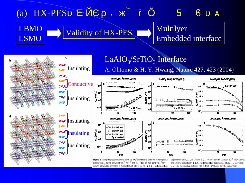
(a) HX-PESのナノスケール新規機能性薄膜への応用LBMOLSMO
MultilyerEmbedded interface
Validity of HX-PES
LaAlO3/SrTiO3 InterfaceA. Ohtomo & H. Y. Hwang, Nature 427, 423 (2004)Insulating
Insulating
Insulating
Insulating
Conductive
Insulating