April 5, 2012
BT33 Datasheet
Amp’ed RF Technology, Inc.
Phone: +1 408 213-9530 | Fax: 408-213-9533 | E-mail: [email protected] Address : 1879 Lundy Ave, ste. 138, San Jose, CA 95131
电话:+86 022-83945100 | 传真:+86 022-83945100 转 111 | E-mail: [email protected]
地址:天津市华苑产业区海泰西路 18 号西 3B-202(300384)
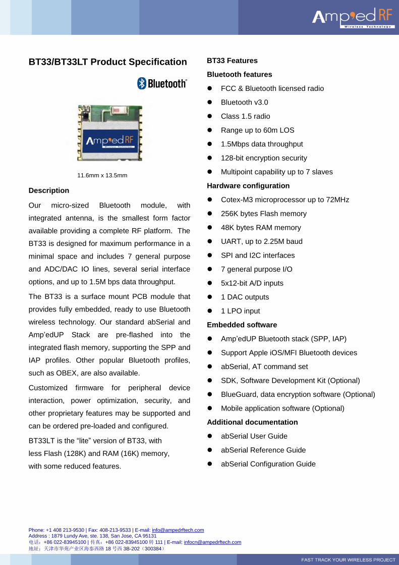
BT33/BT33LT Product Specification
11.6mm x 13.5mm
Description
Our micro-sized Bluetooth module, with
integrated antenna, is the smallest form factor
available providing a complete RF platform. The
BT33 is designed for maximum performance in a
minimal space and includes 7 general purpose
and ADC/DAC IO lines, several serial interface
options, and up to 1.5M bps data throughput.
The BT33 is a surface mount PCB module that
provides fully embedded, ready to use Bluetooth
wireless technology. Our standard abSerial and
Amp’edUP Stack are pre-flashed into the
integrated flash memory, supporting the SPP and
IAP profiles. Other popular Bluetooth profiles,
such as OBEX, are also available.
Customized firmware for peripheral device
interaction, power optimization, security, and
other proprietary features may be supported and
can be ordered pre-loaded and configured.
BT33LT is the “lite” version of BT33, with
less Flash (128K) and RAM (16K) memory,
with some reduced features.
BT33 Features
Bluetooth features
FCC & Bluetooth licensed radio
Bluetooth v3.0
Class 1.5 radio
Range up to 60m LOS
1.5Mbps data throughput
128-bit encryption security
Multipoint capability up to 7 slaves
Hardware configuration
Cotex-M3 microprocessor up to 72MHz
256K bytes Flash memory
48K bytes RAM memory
UART, up to 2.25M baud
SPI and I2C interfaces
7 general purpose I/O
5x12-bit A/D inputs
1 DAC outputs
1 LPO input
Embedded software
Amp’edUP Bluetooth stack (SPP, IAP)
Support Apple iOS/MFI Bluetooth devices
abSerial, AT command set
SDK, Software Development Kit (Optional)
BlueGuard, data encryption software (Optional)
Mobile application software (Optional)
Additional documentation
abSerial User Guide
abSerial Reference Guide
abSerial Configuration Guide
Phone: +1 408 213-9530 | Fax: 408-213-9533 | E-mail: [email protected]
Address : 1879 Lundy Ave, ste. 138, San Jose, CA 95131
电话:+86 022-83945100 | 传真:+86 022-83945100 转 111 | E-mail: [email protected]
地址:天津市华苑产业区海泰西路 18 号西 3B-202(300384)
3
Table of Contents
1 Software Architecture.......................................................................................................................................... 4
1.1 Lower Layer Stack .............................................................................................................................................. 4
1.2 Upper Layer Stack: Amp’ed UP .......................................................................................................................... 4
1.3 HCI Interface ....................................................................................................................................................... 4
1.4 AT Command Set: abSerial ................................................................................................................................ 4
2 Hardware Specifications ..................................................................................................................................... 5
2.1 Recommended Operating Conditions ................................................................................................................ 5
2.2 Absolute Maximum Ratings ................................................................................................................................ 5
2.3 Current Consumption .......................................................................................................................................... 5
2.4 Selected RF Characteristics ............................................................................................................................... 6
2.5 I/O Operating Characteristics ............................................................................................................................. 6
2.6 Pin Assignment ................................................................................................................................................... 7
2.7 Pin Placement Diagram (Top View) ................................................................................................................... 8
2.8 Layout Drawing ................................................................................................................................................... 8
3 Module Block Diagram ........................................................................................................................................ 9
4 Hardware Design ................................................................................................................................................. 9
4.1 Module Reflow Installation .................................................................................................................................. 9
4.2 GPIO Interface .................................................................................................................................................. 10
4.3 UART Interface ................................................................................................................................................. 10
4.4 PCB Layout Guidelines ..................................................................................................................................... 11
4.5 Reset Circuit...................................................................................................................................................... 11
4.5.1 External Reset Circuit: .................................................................................................................................. 11
4.5.2 Internal Reset Circuit: ................................................................................................................................... 12
4.6 External LPO Input Circuit ................................................................................................................................. 12
4.7 Apple iOS CP Reference Design ...................................................................................................................... 13
5 Regulatory Compliance .................................................................................................................................... 14
5.1 Modular Approval, FCC and IC ......................................................................................................................... 15
5.2 FCC Label Instructions ...................................................................................................................................... 15
5.3 FCC Label Instructions ...................................................................................................................................... 15
5.4 FCC Label Instructions ...................................................................................................................................... 15
6 Ordering Informatio ............................................................................................................................................ 16
7 BT33LT, Feature Comparison........................................................................................................................... 16
8 Revision History ................................................................................................................................................. 16
Phone: +1 408 213-9530 | Fax: 408-213-9533 | E-mail: [email protected]
Address : 1879 Lundy Ave, ste. 138, San Jose, CA 95131
电话:+86 022-83945100 | 传真:+86 022-83945100 转 111 | E-mail: [email protected]
地址:天津市华苑产业区海泰西路 18 号西 3B-202(300384)
4
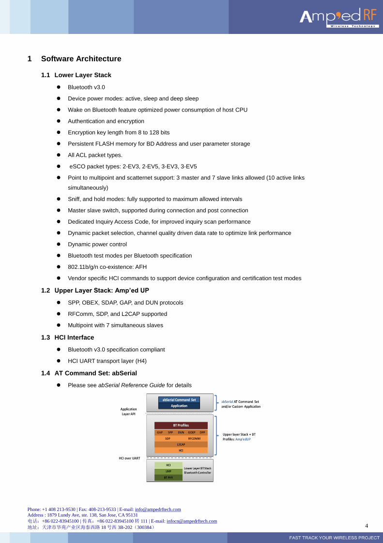
1 Software Architecture
1.1 Lower Layer Stack
Bluetooth v3.0
Device power modes: active, sleep and deep sleep
Wake on Bluetooth feature optimized power consumption of host CPU
Authentication and encryption
Encryption key length from 8 to 128 bits
Persistent FLASH memory for BD Address and user parameter storage
All ACL packet types.
eSCO packet types: 2-EV3, 2-EV5, 3-EV3, 3-EV5
Point to multipoint and scatternet support: 3 master and 7 slave links allowed (10 active links
simultaneously)
Sniff, and hold modes: fully supported to maximum allowed intervals
Master slave switch, supported during connection and post connection
Dedicated Inquiry Access Code, for improved inquiry scan performance
Dynamic packet selection, channel quality driven data rate to optimize link performance
Dynamic power control
Bluetooth test modes per Bluetooth specification
802.11b/g/n co-existence: AFH
Vendor specific HCI commands to support device configuration and certification test modes
1.2 Upper Layer Stack: Amp’ed UP
SPP, OBEX, SDAP, GAP, and DUN protocols
RFComm, SDP, and L2CAP supported
Multipoint with 7 simultaneous slaves
1.3 HCI Interface
Bluetooth v3.0 specification compliant
HCI UART transport layer (H4)
1.4 AT Command Set: abSerial
Please see abSerial Reference Guide for details
Phone: +1 408 213-9530 | Fax: 408-213-9533 | E-mail: [email protected]
Address : 1879 Lundy Ave, ste. 138, San Jose, CA 95131
电话:+86 022-83945100 | 传真:+86 022-83945100 转 111 | E-mail: [email protected]
地址:天津市华苑产业区海泰西路 18 号西 3B-202(300384)
5
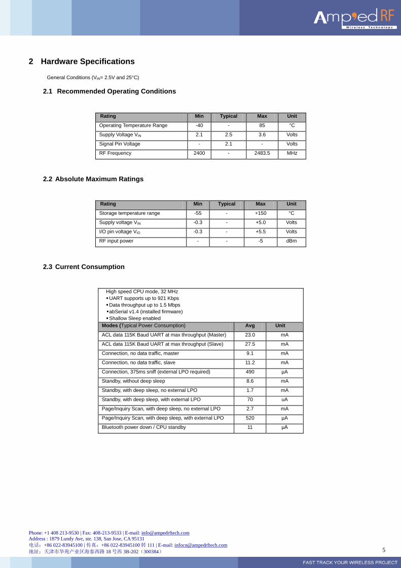
2 Hardware Specifications
General Conditions (VIN= 2.5V and 25°C)
2.1 Recommended Operating Conditions
Rating Min Typical Max Unit
Operating Temperature Range -40 - 85 °C
Supply Voltage VIN 2.1 2.5 3.6 Volts
Signal Pin Voltage - 2.1 - Volts
RF Frequency 2400 - 2483.5 MHz
2.2 Absolute Maximum Ratings
Rating Min Typical Max Unit
Storage temperature range -55 - +150 °C
Supply voltage VIN -0.3 - +5.0 Volts
I/O pin voltage VIO -0.3 - +5.5 Volts
RF input power - - -5 dBm
2.3 Current Consumption
High speed CPU mode, 32 MHz
UART supports up to 921 Kbps
Data throughput up to 1.5 Mbps
abSerial v1.4 (installed firmware)
Shallow Sleep enabled
Modes (Typical Power Consumption) Avg Unit
ACL data 115K Baud UART at max throughput (Master) 23.0 mA
ACL data 115K Baud UART at max throughput (Slave) 27.5 mA
Connection, no data traffic, master 9.1 mA
Connection, no data traffic, slave 11.2 mA
Connection, 375ms sniff (external LPO required) 490 µA
Standby, without deep sleep 8.6 mA
Standby, with deep sleep, no external LPO 1.7 mA
Standby, with deep sleep, with external LPO 70 uA
Page/Inquiry Scan, with deep sleep, no external LPO 2.7 mA
Page/Inquiry Scan, with deep sleep, with external LPO 520 µA
Bluetooth power down / CPU standby 11 μA
Phone: +1 408 213-9530 | Fax: 408-213-9533 | E-mail: [email protected]
Address : 1879 Lundy Ave, ste. 138, San Jose, CA 95131
电话:+86 022-83945100 | 传真:+86 022-83945100 转 111 | E-mail: [email protected]
地址:天津市华苑产业区海泰西路 18 号西 3B-202(300384)
6
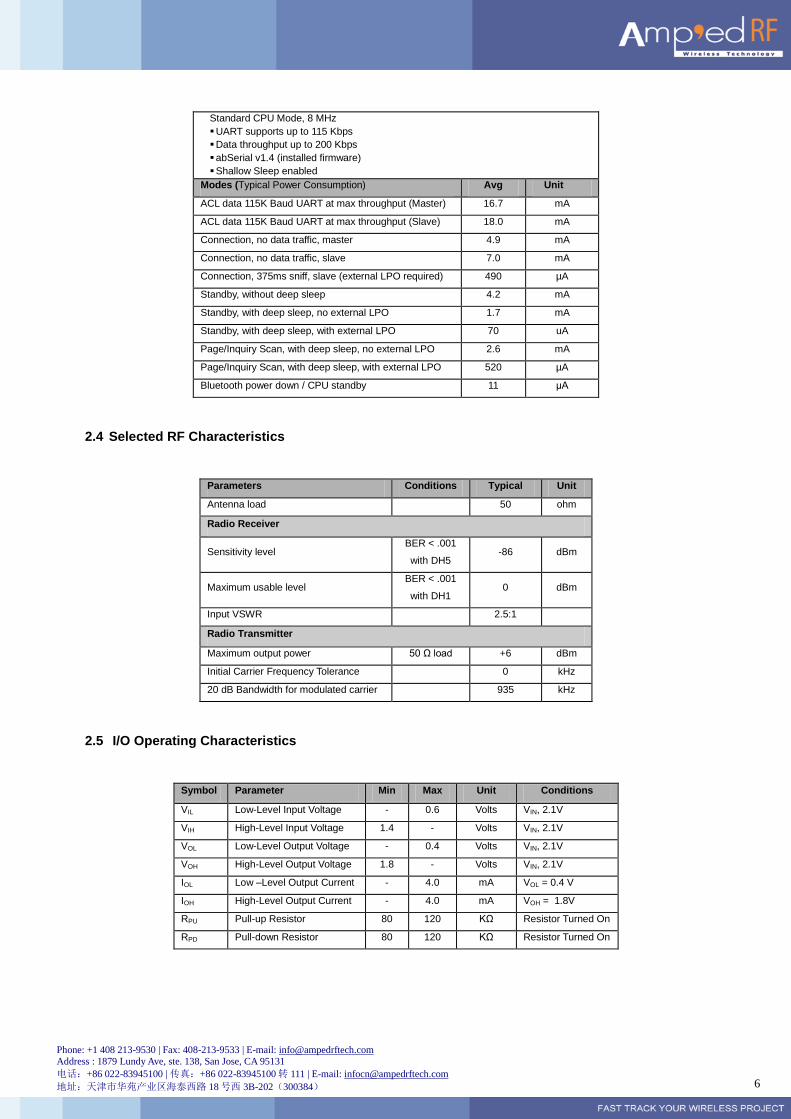
Standard CPU Mode, 8 MHz
UART supports up to 115 Kbps
Data throughput up to 200 Kbps
abSerial v1.4 (installed firmware)
Shallow Sleep enabled
Modes (Typical Power Consumption) Avg Unit
ACL data 115K Baud UART at max throughput (Master) 16.7 mA
ACL data 115K Baud UART at max throughput (Slave) 18.0 mA
Connection, no data traffic, master 4.9 mA
Connection, no data traffic, slave 7.0 mA
Connection, 375ms sniff, slave (external LPO required) 490 µA
Standby, without deep sleep 4.2 mA
Standby, with deep sleep, no external LPO 1.7 mA
Standby, with deep sleep, with external LPO 70 uA
Page/Inquiry Scan, with deep sleep, no external LPO 2.6 mA
Page/Inquiry Scan, with deep sleep, with external LPO 520 µA
Bluetooth power down / CPU standby 11 μA
2.4 Selected RF Characteristics
Parameters Conditions Typical Unit
Antenna load 50 ohm
Radio Receiver
Sensitivity level BER < .001
with DH5 -86 dBm
Maximum usable level BER < .001
with DH1 0 dBm
Input VSWR 2.5:1
Radio Transmitter
Maximum output power 50 Ω load +6 dBm
Initial Carrier Frequency Tolerance 0 kHz
20 dB Bandwidth for modulated carrier 935 kHz
2.5 I/O Operating Characteristics
Symbol Parameter Min Max Unit Conditions
VIL Low-Level Input Voltage - 0.6 Volts VIN, 2.1V
VIH High-Level Input Voltage 1.4 - Volts VIN, 2.1V
VOL Low-Level Output Voltage - 0.4 Volts VIN, 2.1V
VOH High-Level Output Voltage 1.8 - Volts VIN, 2.1V
IOL Low –Level Output Current - 4.0 mA VOL = 0.4 V
IOH High-Level Output Current - 4.0 mA VOH = 1.8V
RPU Pull-up Resistor 80 120 KΩ Resistor Turned On
RPD Pull-down Resistor 80 120 KΩ Resistor Turned On
Phone: +1 408 213-9530 | Fax: 408-213-9533 | E-mail: [email protected]
Address : 1879 Lundy Ave, ste. 138, San Jose, CA 95131
电话:+86 022-83945100 | 传真:+86 022-83945100 转 111 | E-mail: [email protected]
地址:天津市华苑产业区海泰西路 18 号西 3B-202(300384)
7
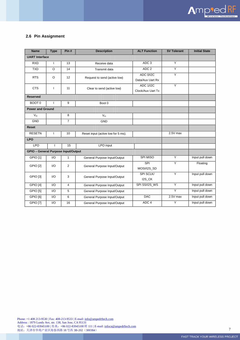
2.6 Pin Assignment
Name Type Pin # Description ALT Function 5V Tolerant Initial State
UART Interface
RXD I 13 Receive data ADC 3 Y
TXD O 14 Transmit data ADC 2 Y
RTS O 12 Request to send (active low) ADC 0/I2C
Data/Aux Uart Rx
Y
CTS I 11 Clear to send (active low) ADC 1/I2C
Clock/Aux Uart Tx
Y
Reserved
BOOT 0 I 9 Boot 0
Power and Ground
Vin 8 Vin
GND 7 GND
Reset
RESETN I 10 Reset input (active low for 5 ms); 2.5V max
LPO
LPO I 15 LPO input
GPIO – General Purpose Input/Output
GPIO [1] I/O 1 General Purpose Input/Output SPI MISO Y Input pull down
GPIO [2] I/O 2 General Purpose Input/Output SPI
MOSI/I2S_SD
Y Floating
GPIO [3] I/O 3 General Purpose Input/Output SPI SCLK/
I2S_CK
Y Input pull down
GPIO [4] I/O 4 General Purpose Input/Output SPI SS/I2S_WS Y Input pull down
GPIO [5] I/O 5 General Purpose Input/Output Y Input pull down
GPIO [6] I/O 6 General Purpose Input/Output DAC 2.5V max Input pull down
GPIO [7] I/O 16 General Purpose Input/Output ADC 4 Y Input pull down
Phone: +1 408 213-9530 | Fax: 408-213-9533 | E-mail: [email protected]
Address : 1879 Lundy Ave, ste. 138, San Jose, CA 95131
电话:+86 022-83945100 | 传真:+86 022-83945100 转 111 | E-mail: [email protected]
地址:天津市华苑产业区海泰西路 18 号西 3B-202(300384)
8
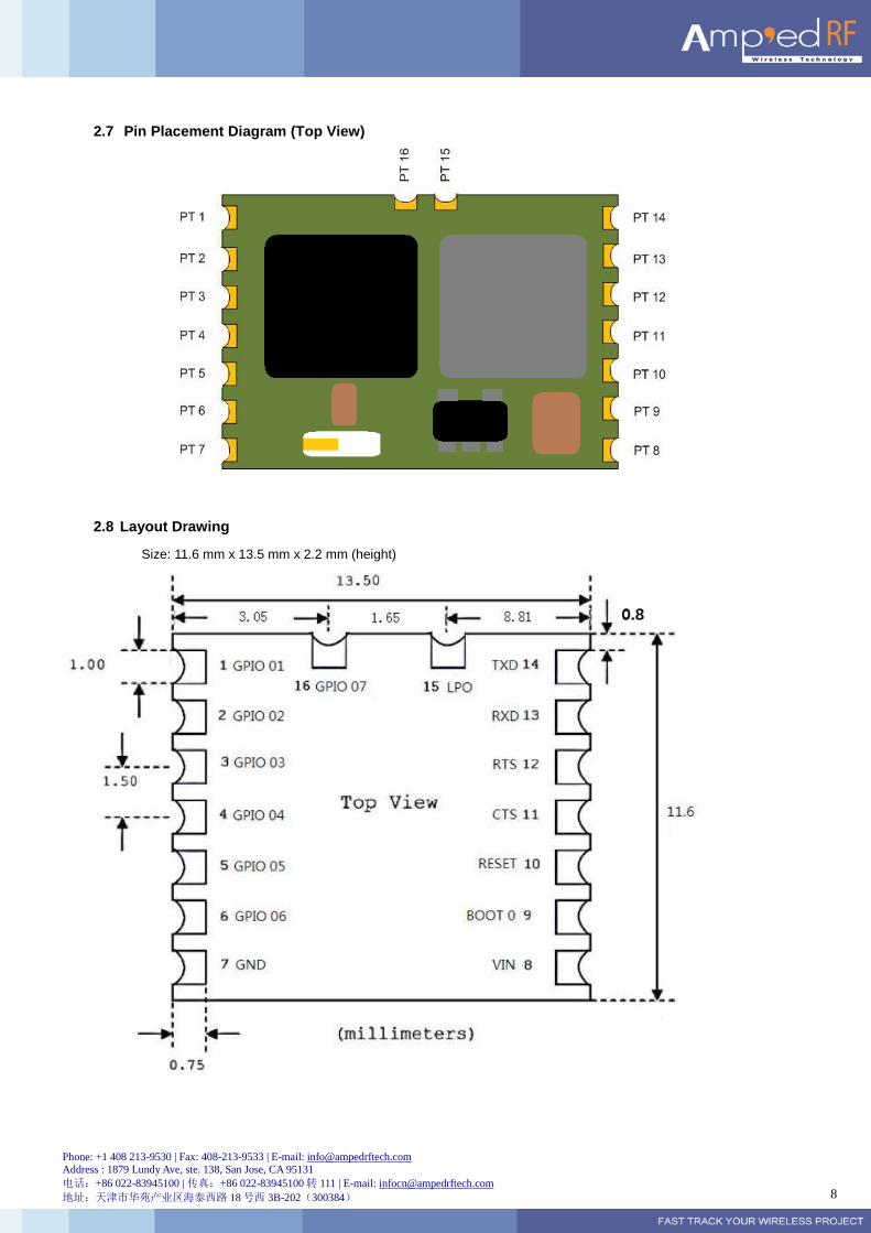
2.7 Pin Placement Diagram (Top View)
2.8 Layout Drawing
Size: 11.6 mm x 13.5 mm x 2.2 mm (height)
Phone: +1 408 213-9530 | Fax: 408-213-9533 | E-mail: [email protected]
Address : 1879 Lundy Ave, ste. 138, San Jose, CA 95131
电话:+86 022-83945100 | 传真:+86 022-83945100 转 111 | E-mail: [email protected]
地址:天津市华苑产业区海泰西路 18 号西 3B-202(300384)
9
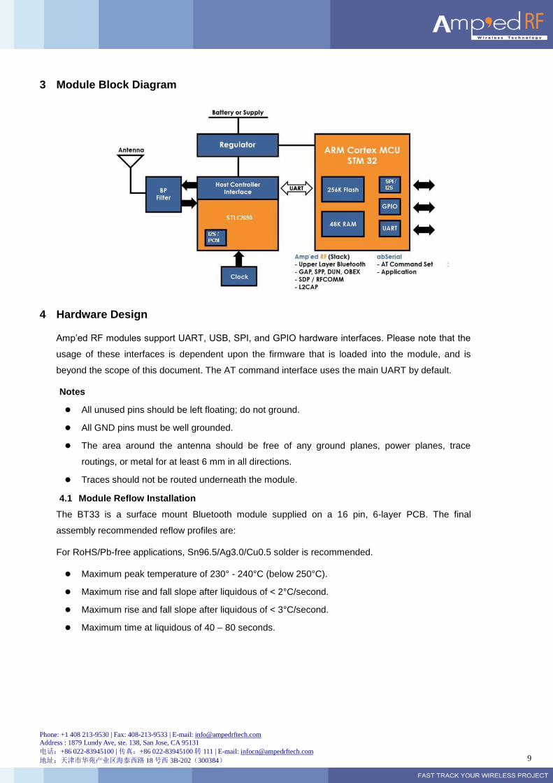
3 Module Block Diagram
4 Hardware Design
Amp’ed RF modules support UART, USB, SPI, and GPIO hardware interfaces. Please note that the
usage of these interfaces is dependent upon the firmware that is loaded into the module, and is
beyond the scope of this document. The AT command interface uses the main UART by default.
Notes
All unused pins should be left floating; do not ground.
All GND pins must be well grounded.
The area around the antenna should be free of any ground planes, power planes, trace
routings, or metal for at least 6 mm in all directions.
Traces should not be routed underneath the module.
4.1 Module Reflow Installation
The BT33 is a surface mount Bluetooth module supplied on a 16 pin, 6-layer PCB. The final
assembly recommended reflow profiles are:
For RoHS/Pb-free applications, Sn96.5/Ag3.0/Cu0.5 solder is recommended.
Maximum peak temperature of 230° - 240°C (below 250°C).
Maximum rise and fall slope after liquidous of < 2°C/second.
Maximum rise and fall slope after liquidous of < 3°C/second.
Maximum time at liquidous of 40 – 80 seconds.
Phone: +1 408 213-9530 | Fax: 408-213-9533 | E-mail: [email protected]
Address : 1879 Lundy Ave, ste. 138, San Jose, CA 95131
电话:+86 022-83945100 | 传真:+86 022-83945100 转 111 | E-mail: [email protected]
地址:天津市华苑产业区海泰西路 18 号西 3B-202(300384)
10
4.2 GPIO Interface
All GPIOs are capable of sinking and sourcing 4mA of I/O current.
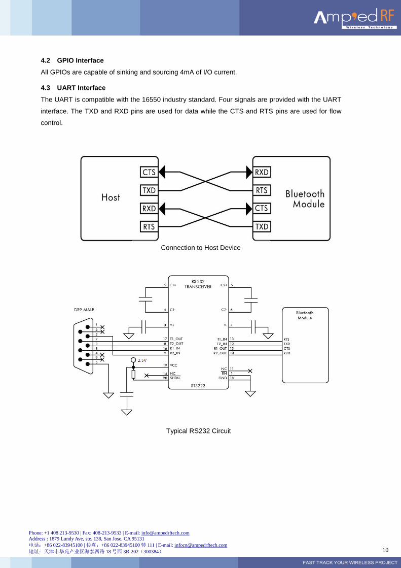
4.3 UART Interface
The UART is compatible with the 16550 industry standard. Four signals are provided with the UART
interface. The TXD and RXD pins are used for data while the CTS and RTS pins are used for flow
control.
Typical RS232 Circuit
Connection to Host Device
Phone: +1 408 213-9530 | Fax: 408-213-9533 | E-mail: [email protected]
Address : 1879 Lundy Ave, ste. 138, San Jose, CA 95131
电话:+86 022-83945100 | 传真:+86 022-83945100 转 111 | E-mail: [email protected]
地址:天津市华苑产业区海泰西路 18 号西 3B-202(300384)
11
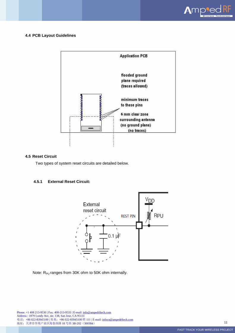
4.4 PCB Layout Guidelines
4.5 Reset Circuit
Two types of system reset circuits are detailed below.
4.5.1 External Reset Circuit:
Note: RPU ranges from 30K ohm to 50K ohm internally.
Phone: +1 408 213-9530 | Fax: 408-213-9533 | E-mail: [email protected]
Address : 1879 Lundy Ave, ste. 138, San Jose, CA 95131
电话:+86 022-83945100 | 传真:+86 022-83945100 转 111 | E-mail: [email protected]
地址:天津市华苑产业区海泰西路 18 号西 3B-202(300384)
12
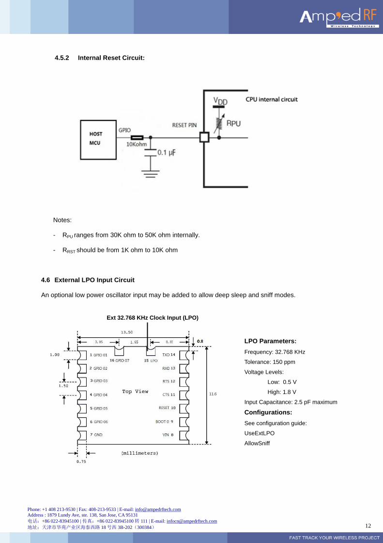
4.5.2 Internal Reset Circuit:
Notes:
- RPU ranges from 30K ohm to 50K ohm internally.
- RRST should be from 1K ohm to 10K ohm
4.6 External LPO Input Circuit
An optional low power oscillator input may be added to allow deep sleep and sniff modes.
LPO Parameters:
Frequency: 32.768 KHz
Tolerance: 150 ppm
Voltage Levels:
Low: 0.5 V
High: 1.8 V
Input Capacitance: 2.5 pF maximum
Configurations:
See configuration guide:
UseExtLPO
AllowSniff
Ext 32.768 KHz Clock Input (LPO)
Phone: +1 408 213-9530 | Fax: 408-213-9533 | E-mail: [email protected]
Address : 1879 Lundy Ave, ste. 138, San Jose, CA 95131
电话:+86 022-83945100 | 传真:+86 022-83945100 转 111 | E-mail: [email protected]
地址:天津市华苑产业区海泰西路 18 号西 3B-202(300384)
13
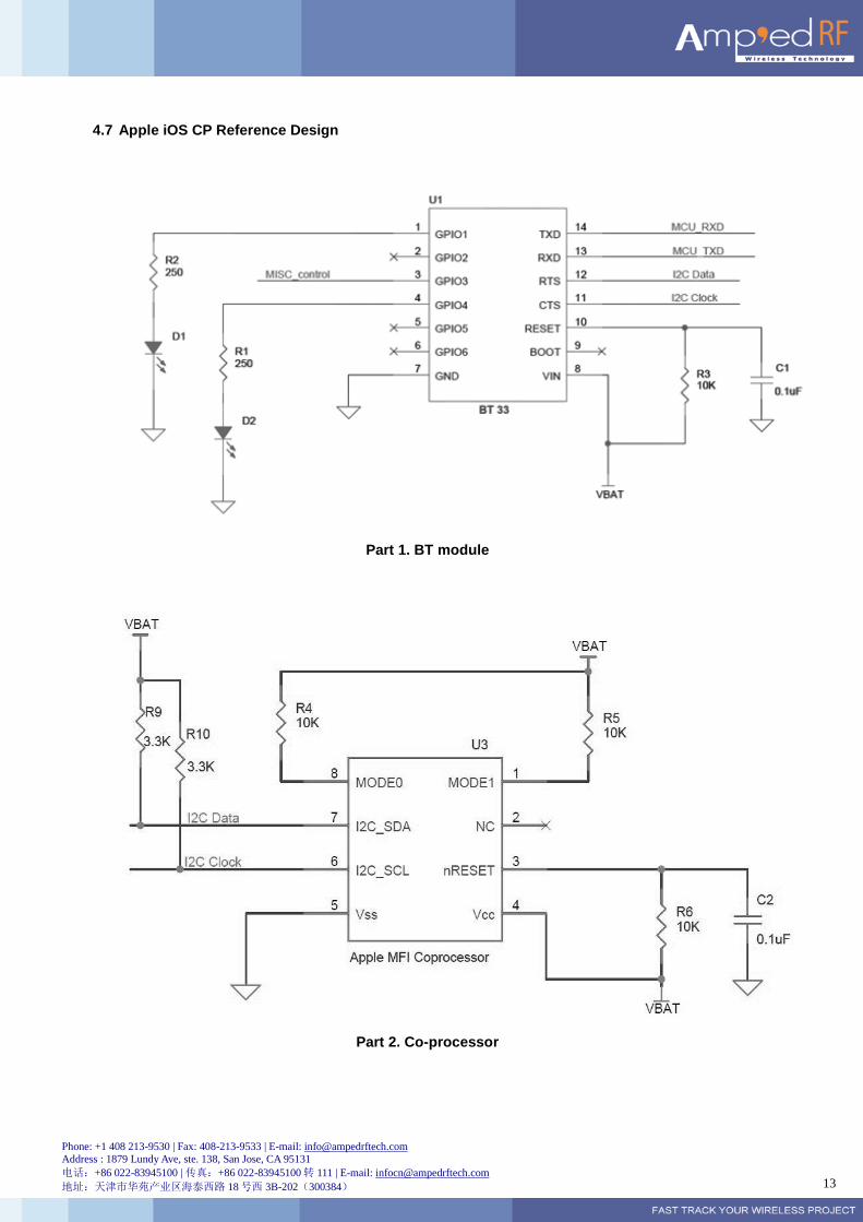
4.7 Apple iOS CP Reference Design
Part 1. BT module
Part 2. Co-processor
Phone: +1 408 213-9530 | Fax: 408-213-9533 | E-mail: [email protected]
Address : 1879 Lundy Ave, ste. 138, San Jose, CA 95131
电话:+86 022-83945100 | 传真:+86 022-83945100 转 111 | E-mail: [email protected]
地址:天津市华苑产业区海泰西路 18 号西 3B-202(300384)
14
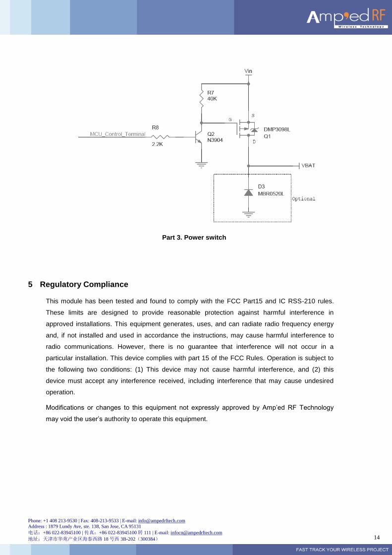
Part 3. Power switch
5 Regulatory Compliance
This module has been tested and found to comply with the FCC Part15 and IC RSS-210 rules.
These limits are designed to provide reasonable protection against harmful interference in
approved installations. This equipment generates, uses, and can radiate radio frequency energy
and, if not installed and used in accordance the instructions, may cause harmful interference to
radio communications. However, there is no guarantee that interference will not occur in a
particular installation. This device complies with part 15 of the FCC Rules. Operation is subject to
the following two conditions: (1) This device may not cause harmful interference, and (2) this
device must accept any interference received, including interference that may cause undesired
operation.
Modifications or changes to this equipment not expressly approved by Amp’ed RF Technology
may void the user’s authority to operate this equipment.
Phone: +1 408 213-9530 | Fax: 408-213-9533 | E-mail: [email protected]
Address : 1879 Lundy Ave, ste. 138, San Jose, CA 95131
电话:+86 022-83945100 | 传真:+86 022-83945100 转 111 | E-mail: [email protected]
地址:天津市华苑产业区海泰西路 18 号西 3B-202(300384)
15
5.1 Modular Approval, FCC and IC
FCC ID: X3ZBTMOD4
IC: 8828A-MOD4
In accordance with FCC Part 15, the BT33 is listed above as a Limited Modular Transmitter device.
5.2 FCC Label Instructions
The outside of final products that contain a BT33 device must display a label referring to the
enclosed module. This exterior label can use wording such as the following:
Contains Transmitter Module
FCC ID: X3ZBTMOD4
IC: 8828A-MOD4
Any similar wording that expresses the same meaning may be used.
5.3 FCC Label Instructions
CE ID: Expert Opinion N. 0448-ARAM00003
5.4 FCC Label Instructions
Bluetooth QDID: B019224
Phone: +1 408 213-9530 | Fax: 408-213-9533 | E-mail: [email protected]
Address : 1879 Lundy Ave, ste. 138, San Jose, CA 95131
电话:+86 022-83945100 | 传真:+86 022-83945100 转 111 | E-mail: [email protected]
地址:天津市华苑产业区海泰西路 18 号西 3B-202(300384)
16
6 Ordering Information
Part Name Description
BT33 Standard version
BT33-LT Lite version, limited features
7 Feature Comparison
Features BT33 BT33-LT
CPU Speed 72MHz Max. 36MHz Max.
CPU Memory 256K Flash, 48K RAM 128K Flash, 16K RAM
Bluetooth Profile Support SPP, IAP, OBEX, DUN SPP and IAP
Bluetooth Stack Amp’edUP, BT v3.0 Amp’ed UP, BT v3.0
Apple iOS Support Supported Supported
AT Command Interface abSerial abSerial Lite
Multiple Connections 7 Max. 1 Max.
Link Throughput 2M bps Max. 300K bps Max.
Serial Interface UART, I2C, SPI UART, I2C, SPI
General I/O Lines 7 7
A/D Lines 4 4
DAC Lines 1 0
8 Revision History
Data Revision Description
23-June-2011 1 First release
6-April-2012 2 Updated for the LT model
Recommended