Embed Size (px)
Citation preview
龙讯教程
How to calculate band alignment between two semiconductors ?
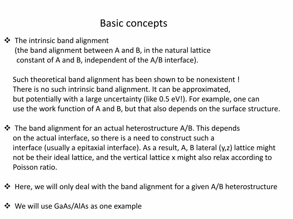
Basic concepts
❖ The intrinsic band alignment(the band alignment between A and B, in the natural latticeconstant of A and B, independent of the A/B interface).
Such theoretical band alignment has been shown to be nonexistent !There is no such intrinsic band alignment. It can be approximated, but potentially with a large uncertainty (like 0.5 eV!). For example, one can use the work function of A and B, but that also depends on the surface structure.
❖ The band alignment for an actual heterostructure A/B. This dependson the actual interface, so there is a need to construct such a interface (usually a epitaxial interface). As a result, A, B lateral (y,z) lattice mightnot be their ideal lattice, and the vertical lattice x might also relax according to Poisson ratio.
❖ Here, we will only deal with the band alignment for a given A/B heterostructure
❖ We will use GaAs/AlAs as one example
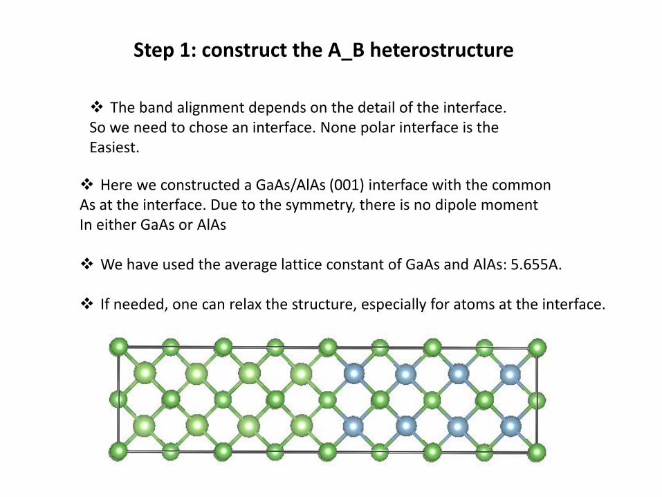
Step 1: construct the A_B heterostructure
❖ The band alignment depends on the detail of the interface. So we need to chose an interface. None polar interface is theEasiest.
❖ Here we constructed a GaAs/AlAs (001) interface with the commonAs at the interface. Due to the symmetry, there is no dipole momentIn either GaAs or AlAs
❖ We have used the average lattice constant of GaAs and AlAs: 5.655A.
❖ If needed, one can relax the structure, especially for atoms at the interface.
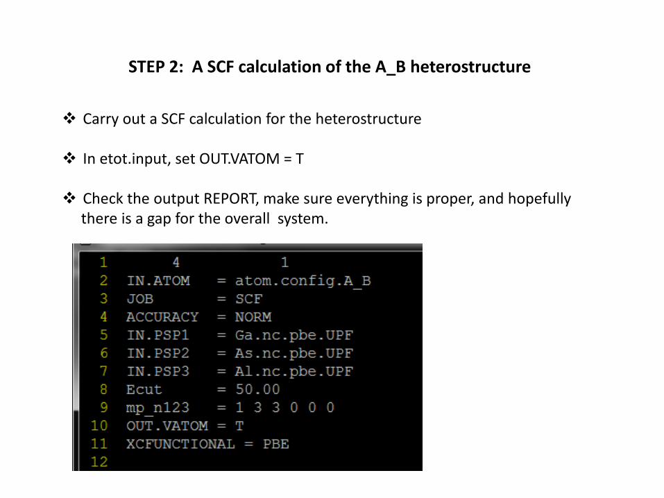
STEP 2: A SCF calculation of the A_B heterostructure
❖ Carry out a SCF calculation for the heterostructure
❖ In etot.input, set OUT.VATOM = T
❖ Check the output REPORT, make sure everything is proper, and hopefullythere is a gap for the overall system.
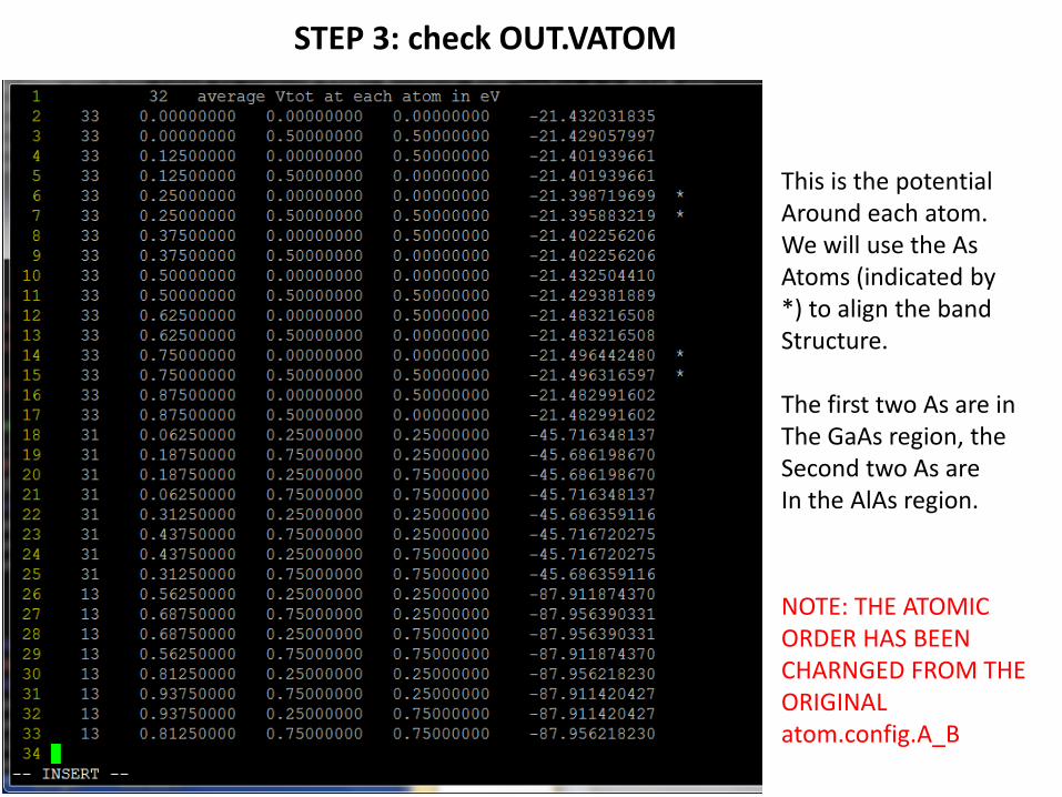
STEP 3: check OUT.VATOM
This is the potentialAround each atom. We will use the AsAtoms (indicated by *) to align the bandStructure.
The first two As are in The GaAs region, theSecond two As areIn the AlAs region.
NOTE: THE ATOMICORDER HAS BEEN CHARNGED FROM THEORIGINAL atom.config.A_B
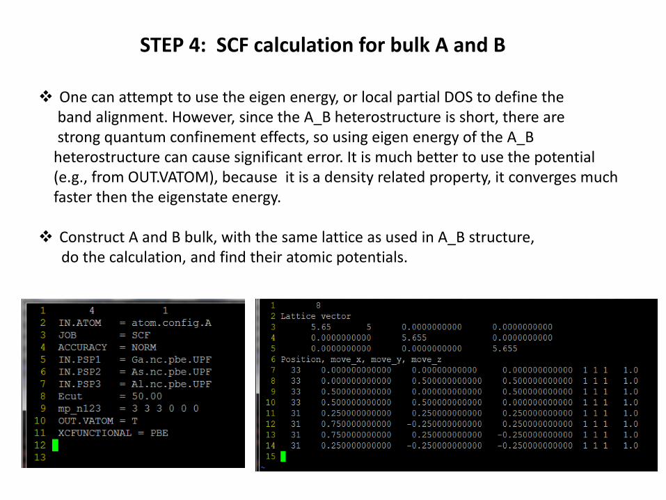
STEP 4: SCF calculation for bulk A and B
❖ One can attempt to use the eigen energy, or local partial DOS to define the band alignment. However, since the A_B heterostructure is short, there arestrong quantum confinement effects, so using eigen energy of the A_B
heterostructure can cause significant error. It is much better to use the potential(e.g., from OUT.VATOM), because it is a density related property, it converges muchfaster then the eigenstate energy.
❖ Construct A and B bulk, with the same lattice as used in A_B structure, do the calculation, and find their atomic potentials.
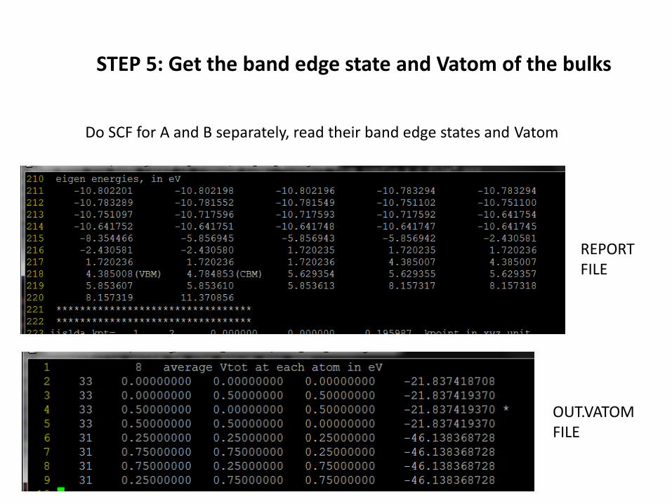
STEP 5: Get the band edge state and Vatom of the bulks
Do SCF for A and B separately, read their band edge states and Vatom
REPORTFILE
OUT.VATOMFILE
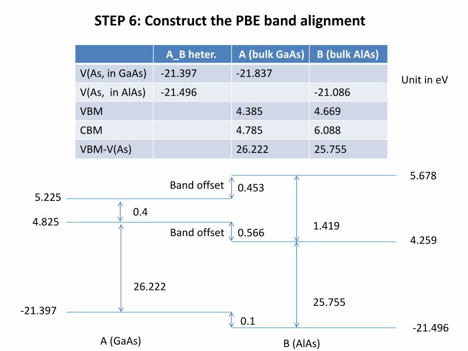
STEP 6: Construct the PBE band alignment
A_B heter. A (bulk GaAs) B (bulk AlAs)
V(As, in GaAs) -21.397 -21.837
V(As, in AlAs) -21.496 -21.086
VBM 4.385 4.669
CBM 4.785 6.088
VBM-V(As) 26.222 25.755
Unit in eV
-21.397
4.825
5.225
-21.496
4.259
5.678
25.755
26.222
0.1
0.566
0.453
1.4190.4
A (GaAs) B (AlAs)
Band offset
Band offset
STEP 7: Correction of PBE band gap error
❖ In above, we have calculated the band offset based on PBE But PBE band gaps are not correct. Here we provide ways to correct this.
❖ For HSE, one way is to repeat the above procedure using HSE throughout.
❖ Here, we provide another simpler way, correct on top of PBE band offsetwith dE_VBM, dE_CBM corrections from the bulk calculation. This can bedone using GW, WKM, or HSE. Here we will use HSE
❖ Note, although in general, the absolute energy for VBM and CBM for a bulk calculation do not have physical meaning, for the same system, and pseudopotential,
on can indeed cross check the results of different methods, like PBE, GW, WKMand HSE. Here we will use HSE (which can be done using SCF or non-SCF, here wewill use SCF).
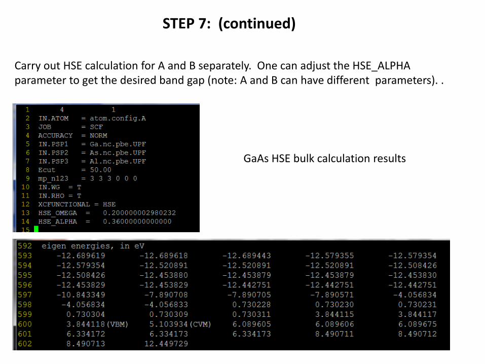
STEP 7: (continued)
Carry out HSE calculation for A and B separately. One can adjust the HSE_ALPHAparameter to get the desired band gap (note: A and B can have different parameters). .
GaAs HSE bulk calculation results
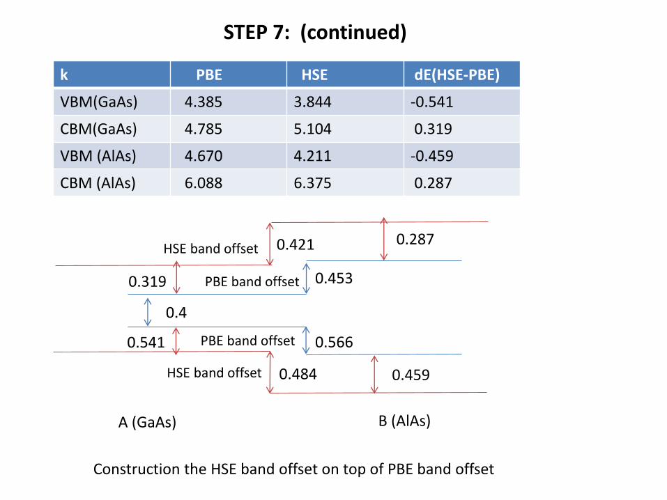
STEP 7: (continued)
k PBE HSE dE(HSE-PBE)
VBM(GaAs) 4.385 3.844 -0.541
CBM(GaAs) 4.785 5.104 0.319
VBM (AlAs) 4.670 4.211 -0.459
CBM (AlAs) 6.088 6.375 0.287
0.566
0.453
0.4
A (GaAs) B (AlAs)
0.287
0.459
0.319
0.541
0.484
0.421HSE band offset
HSE band offset
PBE band offset
PBE band offset
Construction the HSE band offset on top of PBE band offset
STEP 8: band offset at nature lattice constants of A and B
❖ Although we said, there is no absolute intrinsic band level and band alignment, it might still be useful to ask for the band alignment at the natural lattice constants (relaxed) of A and B
❖ The current band alignment is at the epitaxial lattice matched common lattice parameter (at least in the lateral directions).
❖ To get the natural lattice constants, one do a bulk deformation potentialcalculations. In order to get CBM and VBM band offset separately, one
need CBM and VBM absolute deformation potential. They can becalculated using heterostructures consisted with A only (or B only).
❖ See the deformation potential calculation module.
The example files for this module is: GaAs_AlAs_bandalignment.tar