Embed Size (px)
Citation preview
7/31/2019 00855497
http://slidepdf.com/reader/full/00855497 1/7
IEEE TRANSACTIONS ON ANTENNAS AND PROPAGATION, VOL. 48, NO. 5, MAY 2000 777
Experimental Study of a Microstrip Patch Antennawith an -Shaped Probe
C. L. Mak, K. M. Luk , Senior Member, IEEE , K. F. Lee , Fellow, IEEE , and Y. L. Chow
Abstract—The -shaped probe is shown to be an attractivefeed for the thick microstrip antenna (thickness around 10% of the operating wavelength). A parametric study on the rectangularpatch antenna is presented. It is found that the antenna attains36% impedance bandwidth as well as gain band-width and about 7-dBi average gain. A two-element array fed by
-probes is also proposed. Experiments show that the array designcan substantially suppress the cross polarization of the proposedantenna. Both the antennas have stable radiation patterns acrossthe passband. Moreover, the measured resonant frequencies of the proposed antenna agree well with an existing formula and the
-probe does not have much effect on the resonant frequency.
Index Terms—Bandwidth widening, microstrip patch antennas.
I. INTRODUCTION
T HE inherently narrow impedance bandwidth is the
major weakness of a microstrip antenna. Techniques for
bandwidth enhancement have been intensively studied in past
decades. Several methods including the utilization of parasitic
patches [1] and thick substrates [2] have been suggested in the
literature. The stacked geometry resulting from the addition
of parasitic patches will enlarge the size and increase the
complexity in array fabrication, which is especially inconve-
nient for the coplanar case [3]. The technique of employing
a thicker substrate in the coaxially fed method will not only
cause a high level of cross polarization in the -plane, butalso limit the achievable bandwidth to less than 10% of the
resonant frequency due to the increased inductance introduced
by the longer probe required. It is found that the capacitance
introduced by etching a small circular slot on the patch can
cancel out a portion of the probe inductance [4], so that a 16%
bandwidth can be achieved. By etching a U-shaped slot [5], the
bandwidth can be substantially increased, typically to larger
than 30%. Another method to compensate the probe inductance
is the capacitive feeding technique [6]. A small capacitor
patch, connected to the coaxial feed, excites the radiating
patch through capacitive coupling. For the patch antenna with
a thin dielectric substrate (thickness ), the
bandwidth obtained is about 4% [6].Recently, a novel feeding approach employing an -shaped
probe/strip has been proposed [7], [8]. It is already known that
Manuscript received August 27, 1998; revised November24, 1999. This work wassupported by theResearch Grant Council of Hong Kong through theProject9 040 210.
C. L. Mak, K. M. Luk, and Y. L. Chow are with the Department of Elec-tronic Engineering, City Universityof HongKong,Kowloon, HongKong,SAR,China.
K. F. Lee is with the Department of Electrical Engineering, University of Missouri-Columbia, Columbia, MO 65211 USA.
Publisher Item Identifier S 0018-926X(00)04380-5.
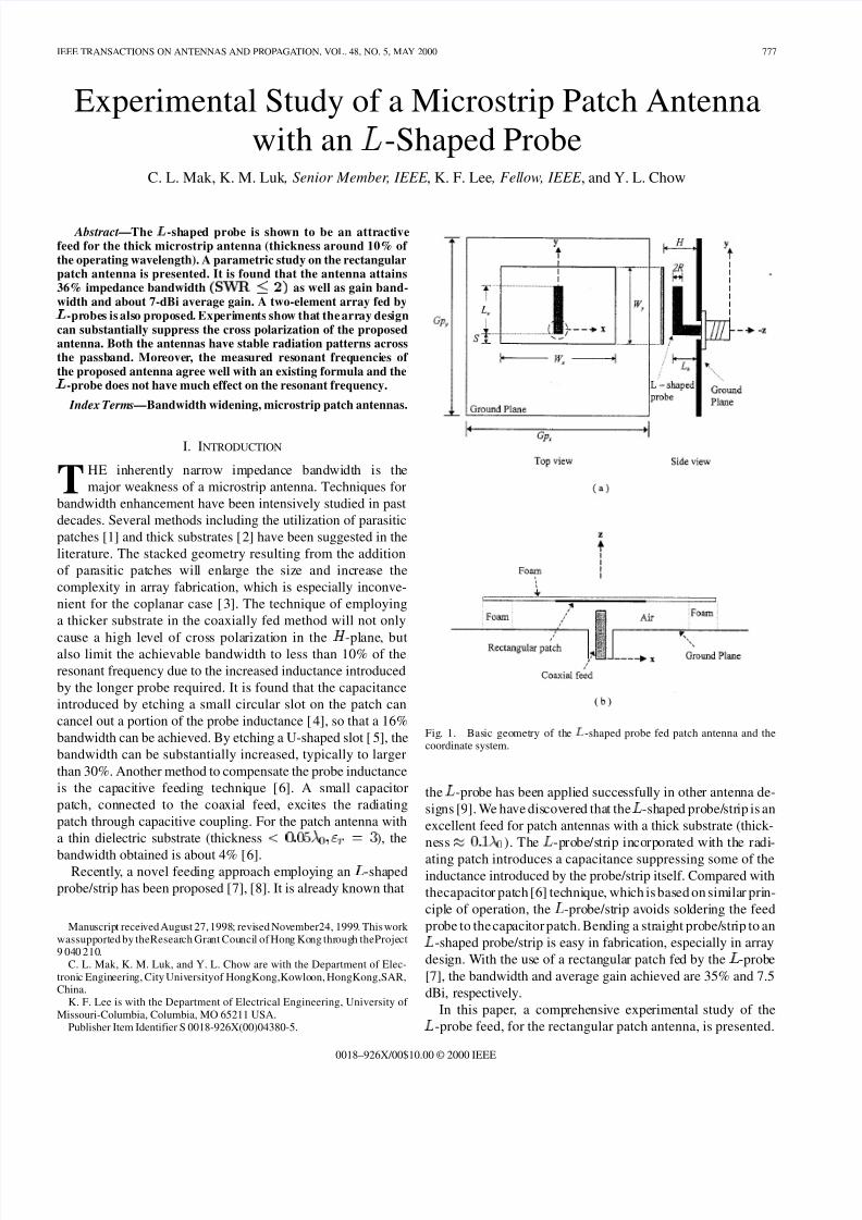
Fig. 1. Basic geometry of the -shaped probe fed patch antenna and thecoordinate system.
the -probe has been applied successfully in other antenna de-
signs [9]. We have discovered that the -shaped probe/strip is an
excellent feed for patch antennas with a thick substrate (thick-
ness ). The -probe/strip incorporated with the radi-
ating patch introduces a capacitance suppressing some of theinductance introduced by the probe/strip itself. Compared with
thecapacitor patch [6] technique, which is based on similar prin-
ciple of operation, the -probe/strip avoids soldering the feed
probe to the capacitor patch. Bending a straight probe/strip to an
-shaped probe/strip is easy in fabrication, especially in array
design. With the use of a rectangular patch fed by the -probe
[7], the bandwidth and average gain achieved are 35% and 7.5
dBi, respectively.
In this paper, a comprehensive experimental study of the
-probe feed, for the rectangular patch antenna, is presented.
0018–926X/00$10.00 © 2000 IEEE
7/31/2019 00855497
http://slidepdf.com/reader/full/00855497 2/7
778 IEEE TRANSACTIONS ON ANTENNAS AND PROPAGATION, VOL. 48, NO. 5, MAY 2000
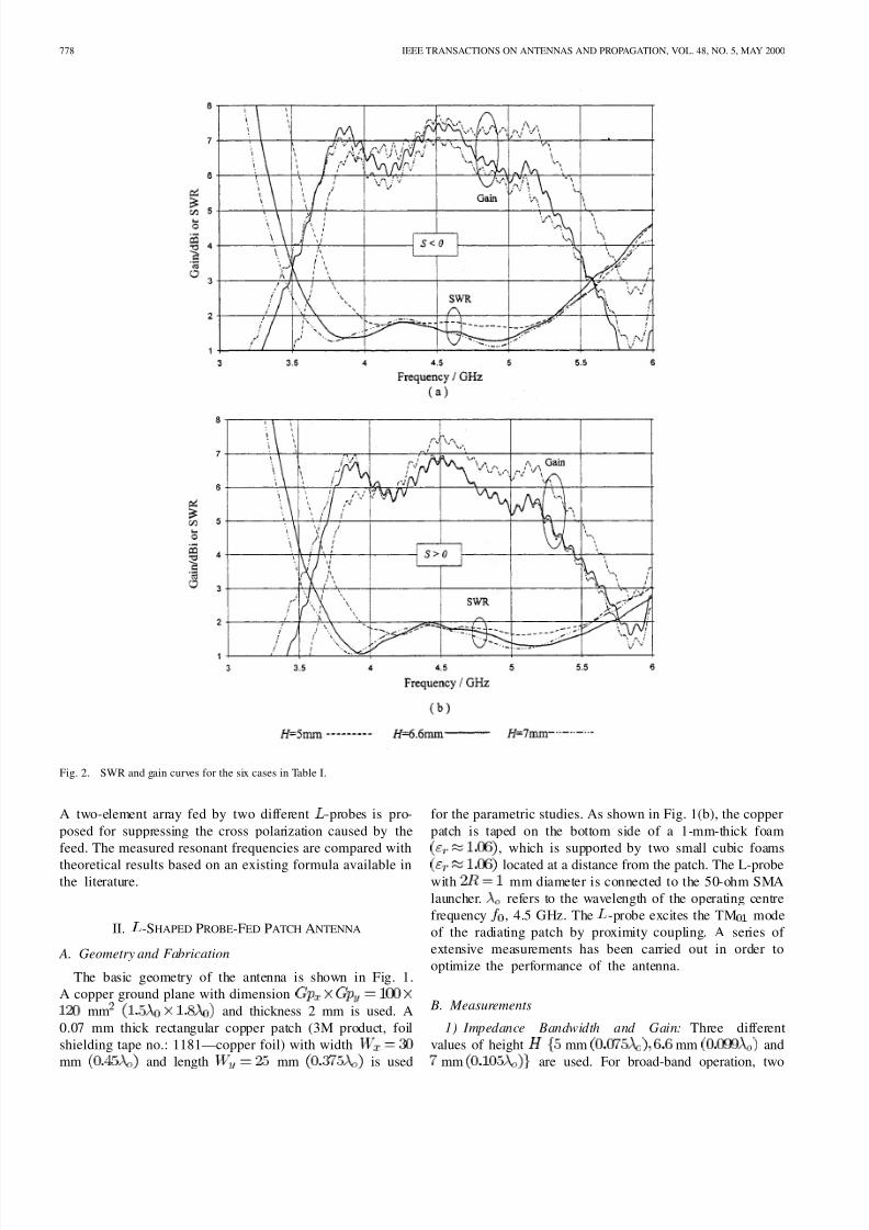
Fig. 2. SWR and gain curves for the six cases in Table I.
A two-element array fed by two different -probes is pro-
posed for suppressing the cross polarization caused by the
feed. The measured resonant frequencies are compared with
theoretical results based on an existing formula available inthe literature.
II. -SHAPED PROBE-FED PATCH ANTENNA
A. Geometry and Fabrication
The basic geometry of the antenna is shown in Fig. 1.
A copper ground plane with dimension
mm and thickness 2 mm is used. A
0.07 mm thick rectangular copper patch (3M product, foil
shielding tape no.: 1181—copper foil) with width
mm and length mm is used
for the parametric studies. As shown in Fig. 1(b), the copper
patch is taped on the bottom side of a 1-mm-thick foam
, which is supported by two small cubic foams
located at a distance from the patch. The L-probewith mm diameter is connected to the 50-ohm SMA
launcher. refers to the wavelength of the operating centre
frequency , 4.5 GHz. The -probe excites the TM mode
of the radiating patch by proximity coupling. A series of
extensive measurements has been carried out in order to
optimize the performance of the antenna.
B. Measurements
1) Impedance Bandwidth and Gain: Three different
values of height mm mm and
mm are used. For broad-band operation, two
7/31/2019 00855497
http://slidepdf.com/reader/full/00855497 3/7
MAK et al.: EXPERIMENTAL STUDY OF MICROSTRIP PATCH ANTENNA 779
TABLE IBANDWIDTH AND GAIN OF THE -SHAPED PROBE FED PATCH ANTENNA
WITH DIFFERENT VALUES OF PARAMETERS
sets of values are found for each value of .
Fig. 2 shows both SWR and gain, measured by a HP8510C
Network Analyzer and a compact range with a HP85301C
Antenna Measurement System, for the six sets of parameters.
The geometric parameters, bandwidth and average gain are
tabulated in Table I. It is checked that the error of all the
dimensions measured are within 1–2%.
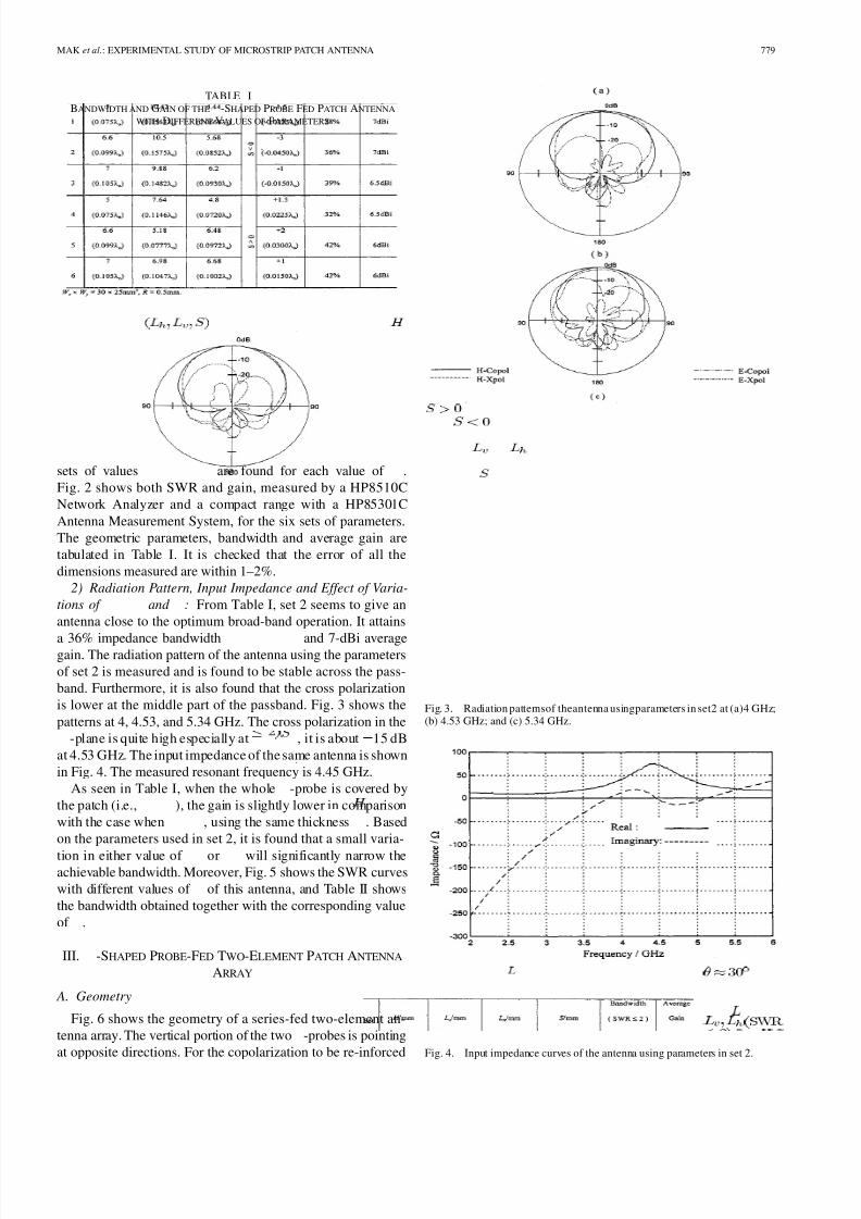
2) Radiation Pattern, Input Impedance and Effect of Varia-
tions of and : From Table I, set 2 seems to give an
antenna close to the optimum broad-band operation. It attains
a 36% impedance bandwidth and 7-dBi averagegain. The radiation pattern of the antenna using the parameters
of set 2 is measured and is found to be stable across the pass-
band. Furthermore, it is also found that the cross polarization
is lower at the middle part of the passband. Fig. 3 shows the
patterns at 4, 4.53, and 5.34 GHz. The cross polarization in the
-plane is quite high especially at , it is about 15 dB
at 4.53 GHz. The input impedance of the same antenna is shown
in Fig. 4. The measured resonant frequency is 4.45 GHz.
As seen in Table I, when the whole -probe is covered by
the patch (i.e., ), the gain is slightly lower in comparison
with the case when , using the same thickness . Based
on the parameters used in set 2, it is found that a small varia-
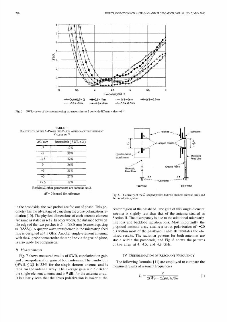
tion in either value of or will significantly narrow theachievable bandwidth. Moreover, Fig. 5 shows the SWR curves
with different values of of this antenna, and Table II shows
the bandwidth obtained together with the corresponding value
of .
III. -SHAPED PROBE-FED TWO-ELEMENT PATCH ANTENNA
ARRAY
A. Geometry
Fig. 6 shows the geometry of a series-fed two-element an-
tenna array. The vertical portion of the two -probes is pointing
at opposite directions. For the copolarization to be re-inforced
Fig. 3. Radiation patternsof theantenna usingparameters in set2 at (a)4 GHz;(b) 4.53 GHz; and (c) 5.34 GHz.
Fig. 4. Input impedance curves of the antenna using parameters in set 2.
7/31/2019 00855497
http://slidepdf.com/reader/full/00855497 4/7
780 IEEE TRANSACTIONS ON ANTENNAS AND PROPAGATION, VOL. 48, NO. 5, MAY 2000
Fig. 5. SWR curves of the antenna using parameters in set 2 but with different values of .
TABLE IIBANDWIDTH OF THE -PROBE FED PATCH ANTENNA WITH DIFFERENT
VALUES OF
in the broadside, the two probes are fed out of phase. This ge-
ometry has the advantage of canceling the cross-polarization ra-
diation [10]. The physical dimensions of each antenna element
are same as stated in set 2. In other words, the distance between
the edge of the two patches is mm (element spacing). A quarter wave transformer in the microstrip feed
line is designed at 4.5 GHz. Another single-element antenna,
with the -probe connected to the stripline via the ground plane,
is also made for comparison.
B. Measurements
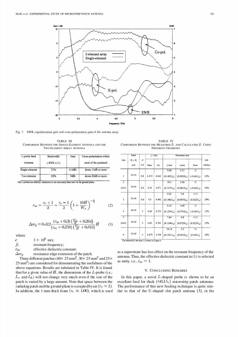
Fig. 7 shows measured results of SWR, copolarization gain
and cross-polarization gain of both antennas. The bandwidth
is 33% for the single-element antenna and is
30% for the antenna array. The average gain is 6.5 dBi for
the single-element antenna and is 9 dBi for the antenna array.
It is clearly seen that the cross polarization is lower at the
Fig. 6. Geometry of the -shaped probes fed two-element antenna array andthe coordinate system.
center region of the passband. The gain of this single-element
antenna is slightly less than that of the antenna studied in
Section II. The discrepancy is due to the additional microstrip
line loss and backlobe radiation loss. Most importantly, the
proposed antenna array attains a cross polarization of 20dB within most of the passband. Table III tabulates the ob-
tained results. The radiation patterns for both antennas are
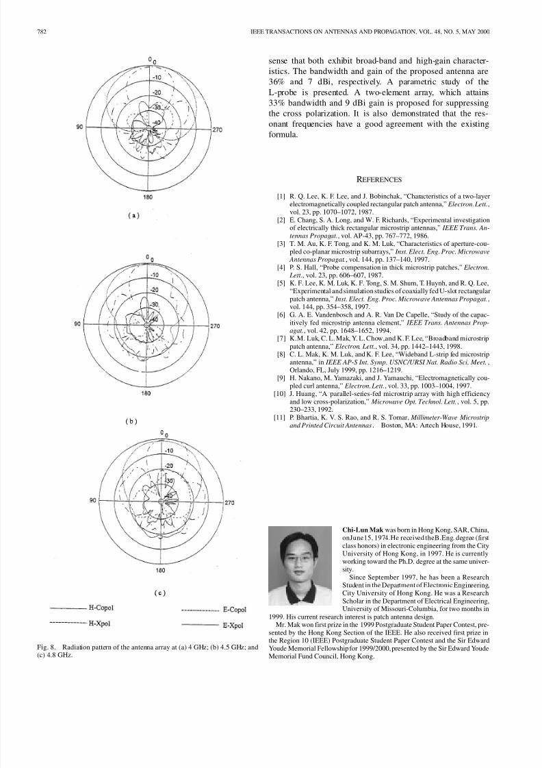
stable within the passbands, and Fig. 8 shows the patterns
of the array at 4, 4.5, and 4.8 GHz.
IV. DETERMINATION OF RESONANT FREQUENCY
The following formulas [11] are employed to compare the
measured results of resonant frequencies
(1)
7/31/2019 00855497
http://slidepdf.com/reader/full/00855497 5/7
MAK et al.: EXPERIMENTAL STUDY OF MICROSTRIP PATCH ANTENNA 781
Fig. 7. SWR copolarization gain and cross-polarization gain of the antenna array.
TABLE IIICOMPARISON BETWEEN THE SINGLE-ELEMENT ANTENNA AND THE
TWO-ELEMENT ARRAY ANTENNA
(2)
(3)
where3 10 m/s;
resonant frequency;
effective dielectric constant;
resonance edge extension of the patch.
Three different patches (40 25 mm , 30 25 mm and 25
25 mm ) are considered for demonstrating the usefulness of the
above equations. Results are tabulated in Table IV. It is found
that for a given value of , the dimensions of the -probe (i.e.,
and ) will not change very much even if the size of the
patch is varied by a large amount. Note that space between the
radiating patch andthe ground plane is occupiedbyair .
In addition, the 1-mm-thick foam , which is used
TABLE IVCOMPARISON BETWEEN THE MEASURED AND CALCULATED USING
DIFFERENT GEOMETRY
as a superstrate has less effect on the resonant frequency of the
antenna. Thus, the effective dielectric constant in (1) is selected
as unity, i.e., .
V. CONCLUDING REMARKS
In this paper, a novel -shaped probe is shown to be an
excellent feed for thick microstrip patch antennas.
The performance of this new feeding technique is quite sim-
ilar to that of the U-shaped slot patch antenna [5], in the
7/31/2019 00855497
http://slidepdf.com/reader/full/00855497 6/7
782 IEEE TRANSACTIONS ON ANTENNAS AND PROPAGATION, VOL. 48, NO. 5, MAY 2000
Fig. 8. Radiation pattern of the antenna array at (a) 4 GHz; (b) 4.5 GHz; and(c) 4.8 GHz.
sense that both exhibit broad-band and high-gain character-
istics. The bandwidth and gain of the proposed antenna are
36% and 7 dBi, respectively. A parametric study of the
L-probe is presented. A two-element array, which attains
33% bandwidth and 9 dBi gain is proposed for suppressing
the cross polarization. It is also demonstrated that the res-
onant frequencies have a good agreement with the existing
formula.
REFERENCES
[1] R. Q. Lee, K. F. Lee, and J. Bobinchak, “Characteristics of a two-layerelectromagnetically coupled rectangular patch antenna,” Electron. Lett.,vol. 23, pp. 1070–1072, 1987.
[2] E. Chang, S. A. Long, and W. F. Richards, “Experimental investigationof electrically thick rectangular microstrip antennas,” IEEE Trans. An-tennas Propagat., vol. AP-43, pp. 767–772, 1986.
[3] T. M. Au, K. F. Tong, and K. M. Luk, “Characteristics of aperture-cou-pled co-planar microstrip subarrays,” Inst. Elect. Eng. Proc. Microwave
Antennas Propagat., vol. 144, pp. 137–140, 1997.
[4] P. S. Hall, “Probe compensation in thick microstrip patches,” Electron. Lett., vol. 23, pp. 606–607, 1987.
[5] K. F. Lee, K. M. Luk, K. F. Tong, S. M. Shum, T. Huynh, and R. Q. Lee,“Experimental and simulation studies of coaxially fed U-slot rectangularpatch antenna,” Inst. Elect. Eng. Proc. Microwave Antennas Propagat.,vol. 144, pp. 354–358, 1997.
[6] G. A. E. Vandenbosch and A. R. Van De Capelle, “Study of the capac-itively fed microstrip antenna element,” IEEE Trans. Antennas Prop-agat., vol. 42, pp. 1648–1652, 1994.
[7] K.M. Luk, C. L. Mak, Y. L. Chow,and K. F. Lee, “Broadband microstrippatch antenna,” Electron. Lett., vol. 34, pp. 1442–1443, 1998.
[8] C. L. Mak, K. M. Luk, and K. F. Lee, “Wideband L-strip fed microstripantenna,” in IEEE AP-S Int. Symp. USNC/URSI Nat. Radio Sci. Meet.,Orlando, FL, July 1999, pp. 1216–1219.
[9] H. Nakano, M. Yamazaki, and J. Yamauchi, “Electromagnetically cou-pled curl antenna,” Electron. Lett., vol. 33, pp. 1003–1004, 1997.
[10] J. Huang, “A parallel-series-fed microstrip array with high efficiency
and low cross-polarization,” Microwave Opt. Technol. Lett., vol. 5, pp.230–233, 1992.[11] P. Bhartia, K. V. S. Rao, and R. S. Tomar, Millimeter-Wave Microstrip
and Printed Circuit Antennas. Boston, MA: Artech House, 1991.
Chi-Lun Mak was born in Hong Kong, SAR, China,
onJune15, 1974.He received theB.Eng. degree (firstclass honors) in electronic engineering from the CityUniversity of Hong Kong, in 1997. He is currentlyworking toward the Ph.D. degree at the same univer-sity.
Since September 1997, he has been a ResearchStudent in the Department of Electronic Engineering,City University of Hong Kong. He was a ResearchScholar in the Department of Electrical Engineering,University of Missouri-Columbia, for two months in
1999. His current research interest is patch antenna design.Mr. Mak won first prize in the 1999 Postgraduate Student Paper Contest, pre-
sented by the Hong Kong Section of the IEEE. He also received first prize inthe Region 10 (IEEE) Postgraduate Student Paper Contest and the Sir EdwardYoude Memorial Fellowship for 1999/2000, presented by the Sir Edward YoudeMemorial Fund Council, Hong Kong.
7/31/2019 00855497
http://slidepdf.com/reader/full/00855497 7/7
MAK et al.: EXPERIMENTAL STUDY OF MICROSTRIP PATCH ANTENNA 783
Kwai-Man Luk (S’80-M’86-SM’94) was born inHong Kong. He received the B.Sc.(Eng.) and Ph.D.degrees in electrical engineering from the Universityof Hong Kong, in 1981 and 1985, respectively.
From June 1985 to November 1987, he was em-ployed as a Lecturer in the Department of ElectronicEngineering, City University of Hong Kong. FromNovember 1987 to January 1992, he joined the De-partment of Electronic Engineering, Chinese Univer-
sity of Hong Kong, as a Lecturer. He returned to theCity University of Hong Kong in January 1992, andis presently a Professor (Chair) of Electronic Engineering. His postgraduatestudies were on Gaussian beam wave theoryand microwaveopen resonators andtheir applications. Currently, his research interests include design of microstrip,planar, and dielectric resonator antennas, microwave measurements, computa-tional electromagnetics. He is the author of four research book chapters, 123 journal papers, and 108 conference papers.
Dr. Luk was the Technical Program Chairperson of the Progress in Electro-magnetics Research Symposium (PIERS 1997) held in Hong Kong in January1997 (an international conference sponsored by the Electromagnetic Academy,USA) and the General Vice-Chairperson of the 1997 Asia-Pacific MicrowaveConference held in Hong Kong in December 1997. He received an Interna-tional Best Paper Award, the Japan Microwave Prize, at the 1994 Asia PacificMicrowave Conference held in Chiba, Japan, in December 1994. He has a com-pleted CERG project rated excellent in 1995. His research proposal submittedto RGC in 1994 was classified in the forefront of experimental research. He is
a Fellow of the Chinese Institute of Electronics and the Institution of ElectricalEngineers and a member of the Electromagnetics Academy.
Kai-Fong Lee (M’73–SM’76-F’97) received theB.Sc. and M.Sc. degrees from Queen’s University,Canada, in 1961 and 1963, respectively, and thePh.D. degree from Cornell University, Ithaca, NY, in1966, all in electrical engineering.
He held research appointments at University of California at San Diego (1966–1967), NationalCenter for Atmospheric Research (1968–1969),National Oceanic and Atmospheric Administration
(1972–1973), UCLA (summer 1975) and NASA(summers of 1986 and 1987). He was and Assis-tant/Associate Professor at the Catholic University of America, Washington,D C (1967–1972), Lecturer/Senior Lecturer/Reader at The Chinese Universityof Hong Kong (1973–1984), and a Professor at the University of Akron, OH(1985–1988). He was the founding Head of the Department of ElectronicEngineering at the City University of Hong Kong (1984–1985). He served asProfessor and Chairman of the Department of Electrical Engineering at theUniversity of Toledo, OH, from 1988 to 1995. Since January 1996, he has beenChairman and LaPierre Professor of the Department of Electrical Engineeringat the University of Missouri-Columbia. He worked on plasma waves andinstabilities from 1965 to 1980 and on antennas since 1981. His publicationsincluding Principles of Antenna Theory (New York: Wiley, 1984), Advancesin Microstrip and Printed Antennas (New York: Wiley, 1997), several invitedbook chapters on microstrip antennas, 127 journal articles, and 96 conferencepapers.
Y. L. Chow, biography and photograph not available at the time of publication.


