Embed Size (px)
Citation preview
2002 IEEE TRANSACTIONS ON NUCLEAR SCIENCE, VOL. 63, NO. 4, AUGUST 2016
Analysis of Soft Error Rates in 65- and 28-nmFD-SOI Processes Depending on BOXRegion Thickness and Body Bias by
Monte-Carlo Based SimulationsKuiyuan Zhang, Shigehiro Umehara, Junki Yamaguchi, Jun Furuta, and Kazutoshi Kobayashi
Abstract— This paper analyzes how body bias and BOX regionthickness affect soft error rates in 65-nm SOTB (Silicon onThin BOX) and 28-nm UTBB (Ultra Thin Body and BOX)FD-SOI processes. Soft errors are induced by alpha-particleand neutron irradiation and the results are then analyzedby Monte Carlo based simulation using PHITS-TCAD. Thealpha-particle-induced single event upset (SEU) cross-section andneutron-induced soft error rate (SER) obtained by simulationare consistent with measurement results. We clarify that SERsdecreased in response to an increase in the BOX thickness forSOTB while SERs in UTBB are independent of BOX thickness.We also discover SOTB develops a higher tolerance to soft errorswhen reverse body bias is applied while UTBB become moresusceptible
Index Terms— FD-SOI, Monte-Carlo simulation, radiationeffects, TCAD.
I. INTRODUCTION
S INGLE Event Upset (SEU) is caused by radiation inducedcharge collecting at a single sensitive node, such as the
drain layer of a single transistor. Radiation-hardened cir-cuits, such as Triple Modular Redundancy (TMR), or DualInterlocked storage CEll (DICE) [1] have been employedto suppress the effects of multi-node charge collection. Sil-icon On Thin BOX (SOTB) [2] and Ultra Thin Body andBOX (UTBB) [3] are two FD-SOI processes with a thin BOXlayer that can efficiently mitigate the charge collected intoa device. Thus, they have higher soft error tolerance thanbulk structures. Since FD-SOI requires no channel doping,threshold voltage variations resulting from fabrication processvariability are reduced. The supply voltage of SOTB can bedecreased to 0.4 V [4]. It is necessary to investigate the softerror tolerance of FD-SOI structure at lower voltages.
The charge collection mechanism has become more com-plex due to device shrinking and increasing circuit densities.The drift and diffusion, as well as the parasitic bipolareffect (PBE) become dominant when a single event occurs
Manuscript received November 8, 2015; revised February 16, 2016 andApril 26, 2016 and June 21, 2016 and July 5, 2016; accepted July 6, 2016.Date of publication July 9, 2016; date of current version August 17, 2016.
The authors are with the Graduate School of Science & Technol-ogy, Kyoto Institute of Technology, Kyoto 606-8585, Japan (e-mail:[email protected]).
Color versions of one or more of the figures in this paper are availableonline at http://ieeexplore.ieee.org.
Digital Object Identifier 10.1109/TNS.2016.2589268
in the circuit [5]. It is difficult to analyze SER while solelydepending on circuit-level simulations such as SPICE; it isfor this reason that TCAD simulation is indispensable. Onedrawback however is that there are only direct ionizationmodels in TCAD simulation and more results are neededto perform dependable comparison with neutron- or alpha-induced SERs. Physical simulations such as indirectly ionizingradiation to get a directly ionized model can increase theaccuracy of TCAD simulation.
Body biasing is commonly used to reduce power consump-tion. The charge collection and well potential are also influ-enced by body bias when a particle hits a device in 130-nm [6]and 65-nm processes [7]. The soft error rates of radiation-hardstructures have undergone dramatic changes due to technologydownscaling. Thus, it is important to also estimate the softerror rates in 65-nm SOTB and 28-nm UTBB structuresresulting from body biasing.
Our goal in this work is to determine the impact thatbody bias and BOX region thickness had on soft errors rates(SER) using two types of processes. We measured alpha- andneutron-induced SERs of 65-nm SOTB and 28-nm UTBBlatches and evaluated the SERs by PHITS-TCAD, aMonte-Carlo based simulation. This simulation is similar toMRED [8], IRT [9] and PHYSERD [10]. PHITS [11] canperform neutron and alpha particle nuclear reactions and there-fore it is commonly used to calculate circuit SERs [12], [13].We compared the SER in FD-SOI device models with vary-ing BOX-layer thickness to find correlations between box-thickness and susceptibility to soft errors.
The rest of this paper is organized as follows:section II introduces the PHITS-TCAD simulationmethodology [14]; section III provides a comparisonbetween PHITS-TCAD simulation results and alpha andneutron irradiation test results [15] and details the resultsobtained depending on thickness of BOX layer and bodybias; section IV provides a final summary and conclusion forthis paper.
II. PHITS-TCAD SIMULATION METHODOLOGY
A. PHITS-TCAD Simulation
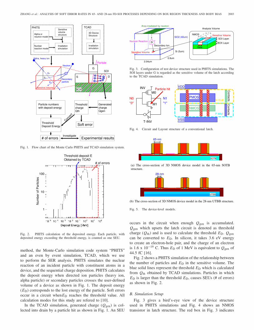
Fig. 1 portrays a flow chart of the proposed SEU simulation.Our calculation model relies on a physics-based simulation
0018-9499 © 2016 IEEE. Personal use is permitted, but republication/redistribution requires IEEE permission.See http://www.ieee.org/publications_standards/publications/rights/index.html for more information.
ZHANG et al.: ANALYSIS OF SOFT ERROR RATES IN 65- AND 28-nm FD-SOI PROCESSES DEPENDING ON BOX REGION THICKNESS AND BODY BIAS 2003
Fig. 1. Flow chart of the Monte Carlo PHITS and TCAD simulation system.
Fig. 2. PHITS calculation of the deposited energy. Each particle, withdeposited energy exceeding the threshold energy, is counted as one SEU.
method, the Monte-Carlo simulation code system “PHITS”and an even by event simulation, TCAD, which we useto perform the SER analysis. PHITS simulates the nuclearreaction of an incident particle with constituent atoms in adevice, and the sequential charge deposition. PHITS calculatesthe deposit energy when directed ion particles (heavy ion,alpha particle) or secondary particles crosses the user-definedvolume of a device as shown in Fig. 1. The deposit energy(ED) corresponds to the lost energy of the particle. Soft errorsoccur in a circuit whenED reaches the threshold value. Allcalculation modes for this study are refered to [10].
In the TCAD simulation, generated charge (Qgen) is col-lected into drain by a particle hit as shown in Fig. 1. An SEU
Fig. 3. Configuration of test device structure used in PHITS simulations. TheSOI layers under G is regarded as the sensitive volume of the latch accordingto the TCAD simulation.
Fig. 4. Circuit and Layout structure of a conventional latch.
Fig. 5. The device-level models.
occurs in the circuit when enough Qgen is accumulated.Qgen which upsets the latch circuit is denoted as thresholdcharge (Qth) and is used to calculate the threshold ED. Qgencan be converted to ED. In silicon, it takes 3.6 eV energyto create an electron-hole pair, and the charge of an electronis 1.6 x 10⁻¹⁹ C. Thus ED of 1 MeV is equivalent to Qgen of44.5 fC [16].
Fig. 2 shows a PHITS simulation of the relationship betweenthe number of particles and ED in the sensitive volume. Theblue solid lines represent the threshold ED which is calculatedfrom Qth obtained by TCAD simulations. Particles in whichED is larger than the threshold ED, causes SEUs (# of errors)as shown in Fig. 2.
B. Simulation Setup
Fig. 3 gives a bird’s-eye view of the device structureused in PHITS simulations and Fig. 4 shows an NMOStransistor in latch structure. The red box in Fig. 3 indicates
2004 IEEE TRANSACTIONS ON NUCLEAR SCIENCE, VOL. 63, NO. 4, AUGUST 2016
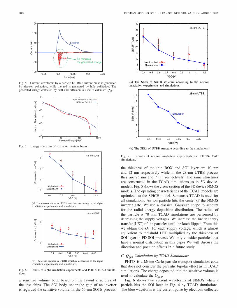
Fig. 6. Current waveforms by a particle hit. Blue current pulse is generatedby electron collection, while the red is generated by hole collection. Thegenerated charge collected by drift and diffusion is used to calculate Qth.
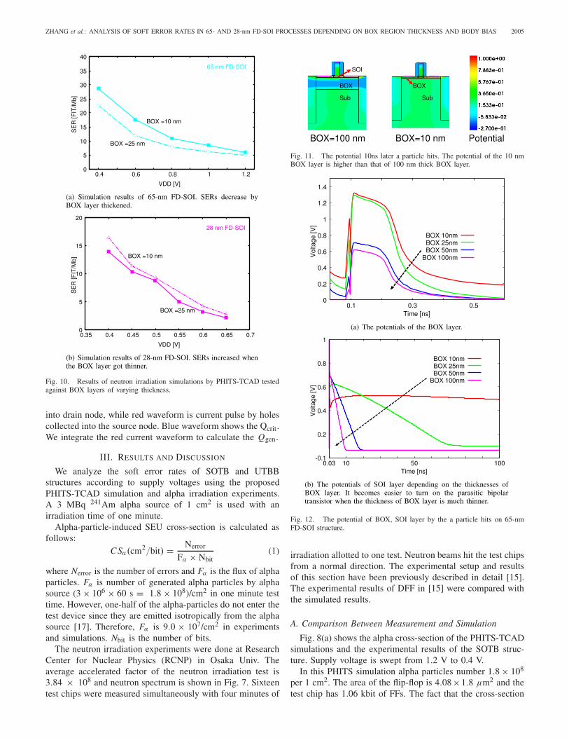
Fig. 7. Energy spectrum of spallation neutron beam.
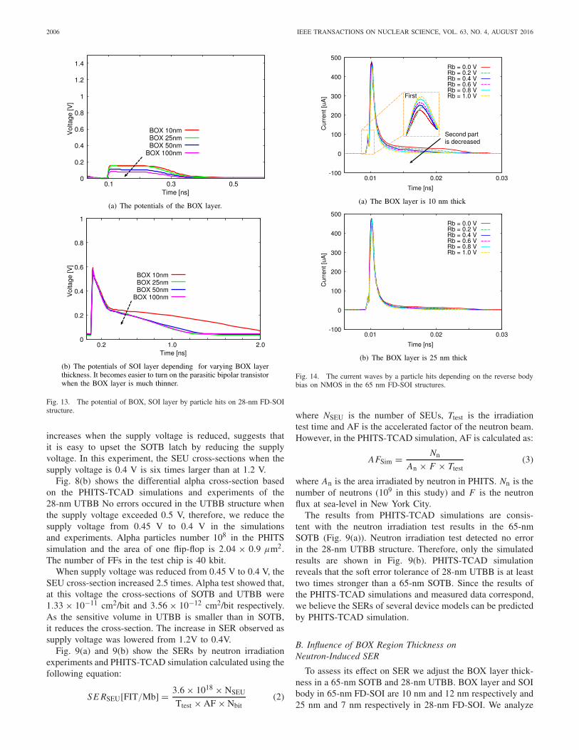
Fig. 8. Results of alpha irradiation experiments and PHITS-TCAD simula-tions.
a sensitive volume built based on the layout structures ofthe test chips. The SOI body under the gate of an inverteris regarded the sensitive volume. In the 65-nm SOTB process,
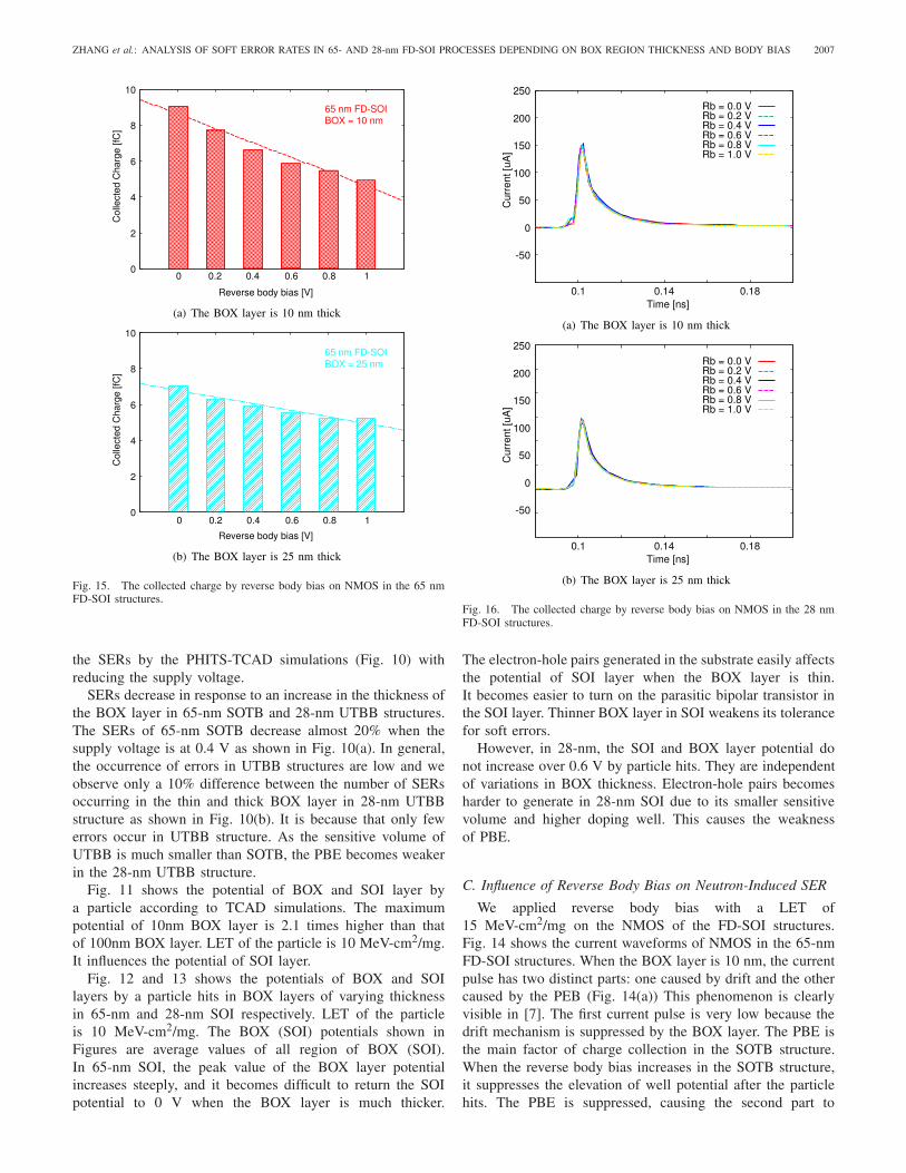
Fig. 9. Results of neutron irradiation experiments and PHITS-TCADsimulations.
the thickness of the thin BOX and SOI layer are 10 nmand 12 nm respectively while in the 28-nm UTBB processthey are 25 nm and 7 nm respectively. The same structuresare constructed in the TCAD simulations as in 3D device-models. Fig. 5 shows the cross-section of the 3D device NMOSmodels. The operating characteristics of the TCAD models areoptimized to the SPICE model. Sentaurus TCAD is used forall simulations. An ion particle hits the center of the NMOSinverter gate. We use a classical Gaussian shape to accountfor the radial energy deposition distribution. The radius ofthe particle is 70 nm. TCAD simulations are performed bydecreasing the supply voltages. We increase the linear energytransfer (LET) of the particles until the latch flipped. From thiswe obtain the Qth for each supply voltage, which is almostequivalent to threshold LET multiplied by the thickness ofSOI layer in FD-SOI process. We only consider particles thathave a normal distribution in this paper We will discuss thedirection and position effects in a future study.
C. Qgen Calculation by TCAD Simulations
PHITS is a Monte Carlo particle transport simulation codethat does not consider the parasitic bipolar effect as in TCADsimulations. The charge deposited into the sensitive volume isused to calculate the Qgen.
Fig. 6 shows two current waveforms of NMOS when aparticle hits the SOI latch in Fig. 4 by TCAD simulations.The blue waveform is the current pulse by electrons collected
ZHANG et al.: ANALYSIS OF SOFT ERROR RATES IN 65- AND 28-nm FD-SOI PROCESSES DEPENDING ON BOX REGION THICKNESS AND BODY BIAS 2005
Fig. 10. Results of neutron irradiation simulations by PHITS-TCAD testedagainst BOX layers of varying thickness.
into drain node, while red waveform is current pulse by holescollected into the source node. Blue waveform shows the Qcrit.We integrate the red current waveform to calculate the Qgen.
III. RESULTS AND DISCUSSION
We analyze the soft error rates of SOTB and UTBBstructures according to supply voltages using the proposedPHITS-TCAD simulation and alpha irradiation experiments.A 3 MBq 241Am alpha source of 1 cm2 is used with anirradiation time of one minute.
Alpha-particle-induced SEU cross-section is calculated asfollows:
C Sα(cm2/bit) = Nerror
Fα × Nbit(1)
where Nerror is the number of errors and Fα is the flux of alphaparticles. Fα is number of generated alpha particles by alphasource (3 × 106 × 60 s = 1.8 × 10⁸)/cm2 in one minute testtime. However, one-half of the alpha-particles do not enter thetest device since they are emitted isotropically from the alphasource [17]. Therefore, Fα is 9.0 × 10⁷/cm2 in experimentsand simulations. Nbit is the number of bits.
The neutron irradiation experiments were done at ResearchCenter for Nuclear Physics (RCNP) in Osaka Univ. Theaverage accelerated factor of the neutron irradiation test is3.84 × 108 and neutron spectrum is shown in Fig. 7. Sixteentest chips were measured simultaneously with four minutes of
Fig. 11. The potential 10ns later a particle hits. The potential of the 10 nmBOX layer is higher than that of 100 nm thick BOX layer.
Fig. 12. The potential of BOX, SOI layer by the a particle hits on 65-nmFD-SOI structure.
irradiation allotted to one test. Neutron beams hit the test chipsfrom a normal direction. The experimental setup and resultsof this section have been previously described in detail [15].The experimental results of DFF in [15] were compared withthe simulated results.
A. Comparison Between Measurement and Simulation
Fig. 8(a) shows the alpha cross-section of the PHITS-TCADsimulations and the experimental results of the SOTB struc-ture. Supply voltage is swept from 1.2 V to 0.4 V.
In this PHITS simulation alpha particles number 1.8 × 10⁸
per 1 cm2. The area of the flip-flop is 4.08×1.8 μm2 and thetest chip has 1.06 kbit of FFs. The fact that the cross-section
2006 IEEE TRANSACTIONS ON NUCLEAR SCIENCE, VOL. 63, NO. 4, AUGUST 2016
Fig. 13. The potential of BOX, SOI layer by particle hits on 28-nm FD-SOIstructure.
increases when the supply voltage is reduced, suggests thatit is easy to upset the SOTB latch by reducing the supplyvoltage. In this experiment, the SEU cross-sections when thesupply voltage is 0.4 V is six times larger than at 1.2 V.
Fig. 8(b) shows the differential alpha cross-section basedon the PHITS-TCAD simulations and experiments of the28-nm UTBB No errors occured in the UTBB structure whenthe supply voltage exceeded 0.5 V, therefore, we reduce thesupply voltage from 0.45 V to 0.4 V in the simulationsand experiments. Alpha particles number 108 in the PHITSsimulation and the area of one flip-flop is 2.04 × 0.9 μm2.The number of FFs in the test chip is 40 kbit.
When supply voltage was reduced from 0.45 V to 0.4 V, theSEU cross-section increased 2.5 times. Alpha test showed that,at this voltage the cross-sections of SOTB and UTBB were1.33 × 10−11 cm2/bit and 3.56 × 10⁻¹² cm2/bit respectively.As the sensitive volume in UTBB is smaller than in SOTB,it reduces the cross-section. The increase in SER observed assupply voltage was lowered from 1.2V to 0.4V.
Fig. 9(a) and 9(b) show the SERs by neutron irradiationexperiments and PHITS-TCAD simulation calculated using thefollowing equation:
SE RSEU[FIT/Mb] = 3.6 × 10¹⁸ × NSEU
Ttest × AF × Nbit(2)
Fig. 14. The current waves by a particle hits depending on the reverse bodybias on NMOS in the 65 nm FD-SOI structures.
where NSEU is the number of SEUs, Ttest is the irradiationtest time and AF is the accelerated factor of the neutron beam.However, in the PHITS-TCAD simulation, AF is calculated as:
AFSim = Nn
An × F × Ttest(3)
where An is the area irradiated by neutron in PHITS. Nn is thenumber of neutrons (109 in this study) and F is the neutronflux at sea-level in New York City.
The results from PHITS-TCAD simulations are consis-tent with the neutron irradiation test results in the 65-nmSOTB (Fig. 9(a)). Neutron irradiation test detected no errorin the 28-nm UTBB structure. Therefore, only the simulatedresults are shown in Fig. 9(b). PHITS-TCAD simulationreveals that the soft error tolerance of 28-nm UTBB is at leasttwo times stronger than a 65-nm SOTB. Since the results ofthe PHITS-TCAD simulations and measured data correspond,we believe the SERs of several device models can be predictedby PHITS-TCAD simulation.
B. Influence of BOX Region Thickness onNeutron-Induced SER
To assess its effect on SER we adjust the BOX layer thick-ness in a 65-nm SOTB and 28-nm UTBB. BOX layer and SOIbody in 65-nm FD-SOI are 10 nm and 12 nm respectively and25 nm and 7 nm respectively in 28-nm FD-SOI. We analyze
ZHANG et al.: ANALYSIS OF SOFT ERROR RATES IN 65- AND 28-nm FD-SOI PROCESSES DEPENDING ON BOX REGION THICKNESS AND BODY BIAS 2007
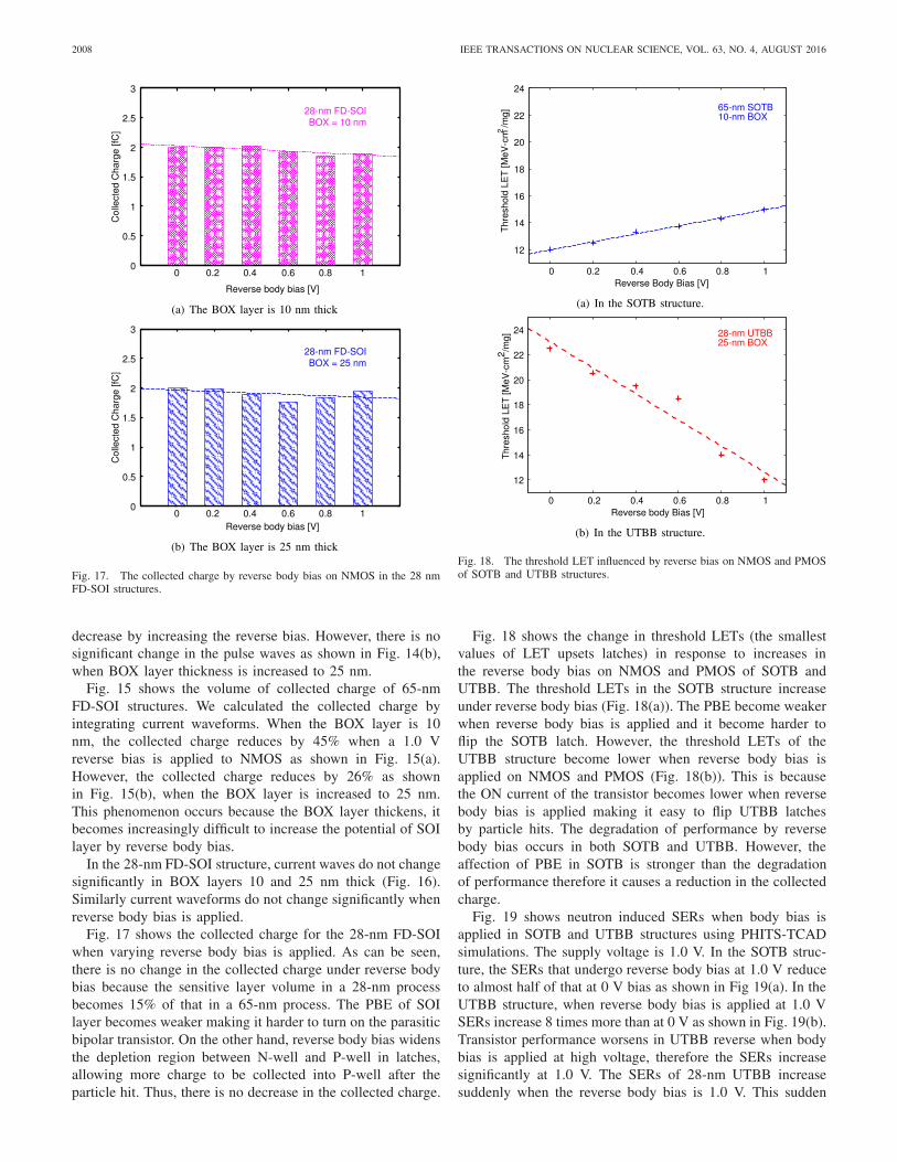
Fig. 15. The collected charge by reverse body bias on NMOS in the 65 nmFD-SOI structures.
the SERs by the PHITS-TCAD simulations (Fig. 10) withreducing the supply voltage.
SERs decrease in response to an increase in the thickness ofthe BOX layer in 65-nm SOTB and 28-nm UTBB structures.The SERs of 65-nm SOTB decrease almost 20% when thesupply voltage is at 0.4 V as shown in Fig. 10(a). In general,the occurrence of errors in UTBB structures are low and weobserve only a 10% difference between the number of SERsoccurring in the thin and thick BOX layer in 28-nm UTBBstructure as shown in Fig. 10(b). It is because that only fewerrors occur in UTBB structure. As the sensitive volume ofUTBB is much smaller than SOTB, the PBE becomes weakerin the 28-nm UTBB structure.
Fig. 11 shows the potential of BOX and SOI layer bya particle according to TCAD simulations. The maximumpotential of 10nm BOX layer is 2.1 times higher than thatof 100nm BOX layer. LET of the particle is 10 MeV-cm2/mg.It influences the potential of SOI layer.
Fig. 12 and 13 shows the potentials of BOX and SOIlayers by a particle hits in BOX layers of varying thicknessin 65-nm and 28-nm SOI respectively. LET of the particleis 10 MeV-cm2/mg. The BOX (SOI) potentials shown inFigures are average values of all region of BOX (SOI).In 65-nm SOI, the peak value of the BOX layer potentialincreases steeply, and it becomes difficult to return the SOIpotential to 0 V when the BOX layer is much thicker.
Fig. 16. The collected charge by reverse body bias on NMOS in the 28 nmFD-SOI structures.
The electron-hole pairs generated in the substrate easily affectsthe potential of SOI layer when the BOX layer is thin.It becomes easier to turn on the parasitic bipolar transistor inthe SOI layer. Thinner BOX layer in SOI weakens its tolerancefor soft errors.
However, in 28-nm, the SOI and BOX layer potential donot increase over 0.6 V by particle hits. They are independentof variations in BOX thickness. Electron-hole pairs becomesharder to generate in 28-nm SOI due to its smaller sensitivevolume and higher doping well. This causes the weaknessof PBE.
C. Influence of Reverse Body Bias on Neutron-Induced SER
We applied reverse body bias with a LET of15 MeV-cm2/mg on the NMOS of the FD-SOI structures.Fig. 14 shows the current waveforms of NMOS in the 65-nmFD-SOI structures. When the BOX layer is 10 nm, the currentpulse has two distinct parts: one caused by drift and the othercaused by the PEB (Fig. 14(a)) This phenomenon is clearlyvisible in [7]. The first current pulse is very low because thedrift mechanism is suppressed by the BOX layer. The PBE isthe main factor of charge collection in the SOTB structure.When the reverse body bias increases in the SOTB structure,it suppresses the elevation of well potential after the particlehits. The PBE is suppressed, causing the second part to
2008 IEEE TRANSACTIONS ON NUCLEAR SCIENCE, VOL. 63, NO. 4, AUGUST 2016
Fig. 17. The collected charge by reverse body bias on NMOS in the 28 nmFD-SOI structures.
decrease by increasing the reverse bias. However, there is nosignificant change in the pulse waves as shown in Fig. 14(b),when BOX layer thickness is increased to 25 nm.
Fig. 15 shows the volume of collected charge of 65-nmFD-SOI structures. We calculated the collected charge byintegrating current waveforms. When the BOX layer is 10nm, the collected charge reduces by 45% when a 1.0 Vreverse bias is applied to NMOS as shown in Fig. 15(a).However, the collected charge reduces by 26% as shownin Fig. 15(b), when the BOX layer is increased to 25 nm.This phenomenon occurs because the BOX layer thickens, itbecomes increasingly difficult to increase the potential of SOIlayer by reverse body bias.
In the 28-nm FD-SOI structure, current waves do not changesignificantly in BOX layers 10 and 25 nm thick (Fig. 16).Similarly current waveforms do not change significantly whenreverse body bias is applied.
Fig. 17 shows the collected charge for the 28-nm FD-SOIwhen varying reverse body bias is applied. As can be seen,there is no change in the collected charge under reverse bodybias because the sensitive layer volume in a 28-nm processbecomes 15% of that in a 65-nm process. The PBE of SOIlayer becomes weaker making it harder to turn on the parasiticbipolar transistor. On the other hand, reverse body bias widensthe depletion region between N-well and P-well in latches,allowing more charge to be collected into P-well after theparticle hit. Thus, there is no decrease in the collected charge.
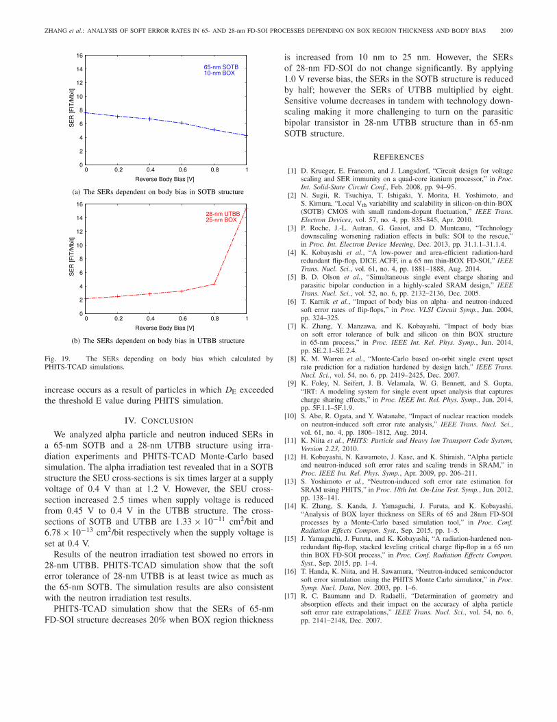
Fig. 18. The threshold LET influenced by reverse bias on NMOS and PMOSof SOTB and UTBB structures.
Fig. 18 shows the change in threshold LETs (the smallestvalues of LET upsets latches) in response to increases inthe reverse body bias on NMOS and PMOS of SOTB andUTBB. The threshold LETs in the SOTB structure increaseunder reverse body bias (Fig. 18(a)). The PBE become weakerwhen reverse body bias is applied and it become harder toflip the SOTB latch. However, the threshold LETs of theUTBB structure become lower when reverse body bias isapplied on NMOS and PMOS (Fig. 18(b)). This is becausethe ON current of the transistor becomes lower when reversebody bias is applied making it easy to flip UTBB latchesby particle hits. The degradation of performance by reversebody bias occurs in both SOTB and UTBB. However, theaffection of PBE in SOTB is stronger than the degradationof performance therefore it causes a reduction in the collectedcharge.
Fig. 19 shows neutron induced SERs when body bias isapplied in SOTB and UTBB structures using PHITS-TCADsimulations. The supply voltage is 1.0 V. In the SOTB struc-ture, the SERs that undergo reverse body bias at 1.0 V reduceto almost half of that at 0 V bias as shown in Fig 19(a). In theUTBB structure, when reverse body bias is applied at 1.0 VSERs increase 8 times more than at 0 V as shown in Fig. 19(b).Transistor performance worsens in UTBB reverse when bodybias is applied at high voltage, therefore the SERs increasesignificantly at 1.0 V. The SERs of 28-nm UTBB increasesuddenly when the reverse body bias is 1.0 V. This sudden
ZHANG et al.: ANALYSIS OF SOFT ERROR RATES IN 65- AND 28-nm FD-SOI PROCESSES DEPENDING ON BOX REGION THICKNESS AND BODY BIAS 2009
Fig. 19. The SERs depending on body bias which calculated byPHITS-TCAD simulations.
increase occurs as a result of particles in which DE exceededthe threshold E value during PHITS simulation.
IV. CONCLUSION
We analyzed alpha particle and neutron induced SERs ina 65-nm SOTB and a 28-nm UTBB structure using irra-diation experiments and PHITS-TCAD Monte-Carlo basedsimulation. The alpha irradiation test revealed that in a SOTBstructure the SEU cross-sections is six times larger at a supplyvoltage of 0.4 V than at 1.2 V. However, the SEU cross-section increased 2.5 times when supply voltage is reducedfrom 0.45 V to 0.4 V in the UTBB structure. The cross-sections of SOTB and UTBB are 1.33 × 10⁻¹¹ cm2/bit and6.78 × 10−13 cm2/bit respectively when the supply voltage isset at 0.4 V.
Results of the neutron irradiation test showed no errors in28-nm UTBB. PHITS-TCAD simulation show that the softerror tolerance of 28-nm UTBB is at least twice as much asthe 65-nm SOTB. The simulation results are also consistentwith the neutron irradiation test results.
PHITS-TCAD simulation show that the SERs of 65-nmFD-SOI structure decreases 20% when BOX region thickness
is increased from 10 nm to 25 nm. However, the SERsof 28-nm FD-SOI do not change significantly. By applying1.0 V reverse bias, the SERs in the SOTB structure is reducedby half; however the SERs of UTBB multiplied by eight.Sensitive volume decreases in tandem with technology down-scaling making it more challenging to turn on the parasiticbipolar transistor in 28-nm UTBB structure than in 65-nmSOTB structure.
REFERENCES
[1] D. Krueger, E. Francom, and J. Langsdorf, “Circuit design for voltagescaling and SER immunity on a quad-core itanium processor,” in Proc.Int. Solid-State Circuit Conf., Feb. 2008, pp. 94–95.
[2] N. Sugii, R. Tsuchiya, T. Ishigaki, Y. Morita, H. Yoshimoto, andS. Kimura, “Local Vth variability and scalability in silicon-on-thin-BOX(SOTB) CMOS with small random-dopant fluctuation,” IEEE Trans.Electron Devices, vol. 57, no. 4, pp. 835–845, Apr. 2010.
[3] P. Roche, J.-L. Autran, G. Gasiot, and D. Munteanu, “Technologydownscaling worsening radiation effects in bulk: SOI to the rescue,”in Proc. Int. Electron Device Meeting, Dec. 2013, pp. 31.1.1–31.1.4.
[4] K. Kobayashi et al., “A low-power and area-efficient radiation-hardredundant flip-flop, DICE ACFF, in a 65 nm thin-BOX FD-SOI,” IEEETrans. Nucl. Sci., vol. 61, no. 4, pp. 1881–1888, Aug. 2014.
[5] B. D. Olson et al., “Simultaneous single event charge sharing andparasitic bipolar conduction in a highly-scaled SRAM design,” IEEETrans. Nucl. Sci., vol. 52, no. 6, pp. 2132–2136, Dec. 2005.
[6] T. Karnik et al., “Impact of body bias on alpha- and neutron-inducedsoft error rates of flip-flops,” in Proc. VLSI Circuit Symp., Jun. 2004,pp. 324–325.
[7] K. Zhang, Y. Manzawa, and K. Kobayashi, “Impact of body biason soft error tolerance of bulk and silicon on thin BOX structurein 65-nm process,” in Proc. IEEE Int. Rel. Phys. Symp., Jun. 2014,pp. SE.2.1–SE.2.4.
[8] K. M. Warren et al., “Monte-Carlo based on-orbit single event upsetrate prediction for a radiation hardened by design latch,” IEEE Trans.Nucl. Sci., vol. 54, no. 6, pp. 2419–2425, Dec. 2007.
[9] K. Foley, N. Seifert, J. B. Velamala, W. G. Bennett, and S. Gupta,“IRT: A modeling system for single event upset analysis that capturescharge sharing effects,” in Proc. IEEE Int. Rel. Phys. Symp., Jun. 2014,pp. 5F.1.1–5F.1.9.
[10] S. Abe, R. Ogata, and Y. Watanabe, “Impact of nuclear reaction modelson neutron-induced soft error rate analysis,” IEEE Trans. Nucl. Sci.,vol. 61, no. 4, pp. 1806–1812, Aug. 2014.
[11] K. Niita et al., PHITS: Particle and Heavy Ion Transport Code System,Version 2.23, 2010.
[12] H. Kobayashi, N. Kawamoto, J. Kase, and K. Shiraish, “Alpha particleand neutron-induced soft error rates and scaling trends in SRAM,” inProc. IEEE Int. Rel. Phys. Symp., Apr. 2009, pp. 206–211.
[13] S. Yoshimoto et al., “Neutron-induced soft error rate estimation forSRAM using PHITS,” in Proc. 18th Int. On-Line Test. Symp., Jun. 2012,pp. 138–141.
[14] K. Zhang, S. Kanda, J. Yamaguchi, J. Furuta, and K. Kobayashi,“Analysis of BOX layer thickness on SERs of 65 and 28nm FD-SOIprocesses by a Monte-Carlo based simulation tool,” in Proc. Conf.Radiation Effects Compon. Syst., Sep. 2015, pp. 1–5.
[15] J. Yamaguchi, J. Furuta, and K. Kobayashi, “A radiation-hardened non-redundant flip-flop, stacked leveling critical charge flip-flop in a 65 nmthin BOX FD-SOI process,” in Proc. Conf. Radiation Effects Compon.Syst., Sep. 2015, pp. 1–4.
[16] T. Handa, K. Niita, and H. Sawamura, “Neutron-induced semiconductorsoft error simulation using the PHITS Monte Carlo simulator,” in Proc.Symp. Nucl. Data, Nov. 2003, pp. 1–6.
[17] R. C. Baumann and D. Radaelli, “Determination of geometry andabsorption effects and their impact on the accuracy of alpha particlesoft error rate extrapolations,” IEEE Trans. Nucl. Sci., vol. 54, no. 6,pp. 2141–2148, Dec. 2007.
![Chapter 7 Correction of Errors [II]: Errors Affecting …proxy.flss.edu.hk/~flssmcwong/S5 Notes/Chapter 7...1 Chapter 7 Correction of Errors [II]: Errors Affecting Trial Balance Agreement](https://img.pdfslide.tips/doc/110x75/5e919753b752cc557f0672e9/chapter-7-correction-of-errors-ii-errors-affecting-proxyflsseduhkflssmcwongs5.jpg)
![Chapter 6 Correction of Errors [I]: Errors Not …proxy.flss.edu.hk/~flssmcwong/S5 Notes/Chapter 6...1 Chapter 6 Correction of Errors [I]: Errors Not Affecting Trial Balance Agreement](https://img.pdfslide.tips/doc/110x75/5e920595f3ae2923c416eecb/chapter-6-correction-of-errors-i-errors-not-proxyflsseduhkflssmcwongs5.jpg)
![SSppoojjkkyy RRAATTHHII JJAAWW--FFLLEEXX NN--FFLLEEXX … · 4.2 TOLERANCE OTVORU A DRÁŽKY PRO PERO TOLERANCE ULOŽENÍ OTVORU V NÁBOJI: Požadované uložení Díra [mm] Tolerance](https://img.pdfslide.tips/doc/110x75/5e18e4bd41a8c136c71922bb/ssppoojjkkyy-rraatthhii-jjaaww-fflleexx-nn-fflleexx-42-tolerance-otvoru-a-drky.jpg)