Embed Size (px)
Citation preview
사 학 논 문
Master’s Thesis
미 체소자 내 액체 속거울
용한 분 학 분
Spectrometric Analysis Using Liquid Metal
Mirrors in a Microfluidic Device
재 규 (崔 在 奎 Choi, Jaekyu)
뇌공학과
Department of Bio and Brain Engineering
KAIST
2010
미 체소자 내 액체 속거울
용한 분 학 분
Spectrometric Analysis Using Liquid Metal
Mirrors in a Microfluidic Device

Spectrometric Analysis Using Liquid Metal
Mirrors in a Microfluidic Device
Advisor: Professor Je-Kyun Park
by
Jaekyu Choi
Department of Bio and Brain Engineering
KAIST
A thesis submitted to the faculty of the KAIST in partial
fulfillment of the requirements for the degree of Master of Science
in Engineering in the Department of Bio and Brain Engineering.
Daejeon, Korea
2009. 12. 22.
Approved by
Professor Je-Kyun Park
(Major Advisor)

미 체소자 내 액체 속거울
용한 분 학 분
재 규
논문 한 과학 원 사학 논문 로 학 논문심사
원회에 심사 통과하 .
2009 12월 22일
심사 원장 균 (인)
심 사 원 남 (인)
심 사 원 훈 (인)
i
MBiS
20083538
재 규. Choi, Jaekyu
Spectrometric Analysis Using Liquid Metal Mirrors in a Microfluidic
Device. 미 체소자 내 액체 속거울 용한 분 학 분
Department of Bio and Brain Engineering. 2010. 32p.
Advisor Prof. Park, Je-Kyun. Text in English
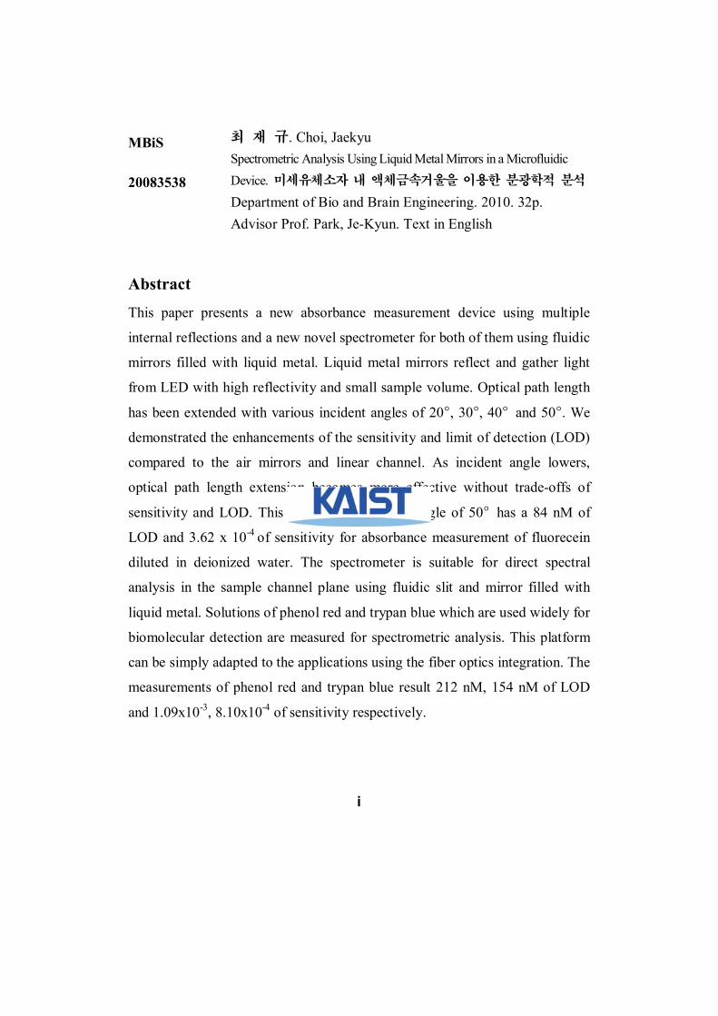
Abstract
This paper presents a new absorbance measurement device using multiple
internal reflections and a new novel spectrometer for both of them using fluidic
mirrors filled with liquid metal. Liquid metal mirrors reflect and gather light
from LED with high reflectivity and small sample volume. Optical path length
has been extended with various incident angles of 20°, 30°, 40° and 50°. We
demonstrated the enhancements of the sensitivity and limit of detection (LOD)
compared to the air mirrors and linear channel. As incident angle lowers,
optical path length extension becomes more effective without trade-offs of
sensitivity and LOD. This device with incident angle of 50° has a 84 nM of
LOD and 3.62 x 10⁻⁴ of sensitivity for absorbance measurement of fluorecein
diluted in deionized water. The spectrometer is suitable for direct spectral
analysis in the sample channel plane using fluidic slit and mirror filled with
liquid metal. Solutions of phenol red and trypan blue which are used widely for
biomolecular detection are measured for spectrometric analysis. This platform
can be simply adapted to the applications using the fiber optics integration. The
measurements of phenol red and trypan blue result 212 nM, 154 nM of LOD
and 1.09x10⁻³, 8.10x10⁻⁴ of sensitivity respectively.
ii
Table of contents
Abstract ········································································································· i
Table of contents ··························································································· ii
Nomenclature ······························································································iii
List of Tables ······························································································· vi
List of Figures ····························································································· vii
1. Introduction ······························································································ 1
1.1 Optical measurements in lab chips ························································ 1
1.2 Research objectives ············································································ 11
2. Materials and Methods ·········································································· 12
2.1 Chip design ························································································ 12
2.2 Fabrication process ············································································· 18
2.3 Experimental setup ············································································· 22
2.4 Evaluation criteria ·············································································· 26
3. Results and Discussions ·········································································· 28
3.1 Optical path extension ········································································ 28
3.2 Spectrometer ······················································································ 28
4. Conclusions ····························································································· 39
4.1 Summary ···························································································· 39
4.2 Further works ····················································································· 40
Summary in Korean ··················································································· 44
Reference ···································································································· 45

iii
Nomenclature
Alphabetic Letters
A Absorbance
c Concentration of solution
d Optical path length
L Length of the sample channel
m Slope of the straight line
sblank Standard deviation of the blank signal
ss standard deviation of the measurement

iv
Greek Letters
ε Absorbance coefficient
θi Incident angle of light

v
Abbreviations
APD Avalanche photodetector
EWOD Electrowetting-on-dielectric
LED Light emitting diode
LOC Lab-on-a-chip
LOD Limit of detection
PDMS Poly(dimethylsiloxane)
PEB Post-exposure bake
POC Point-of-care
MPPC Multi-pixel photon counter
vi
List of Tables
Table 1. Physical properties of liquid metal, Glinstan.
Table 2. List of materials.
Table 3. Comparisons liquid metal mirros to air mirrors and linear channel.
Table 4. Comparisons to other spectrometers.

vii
List of Figures
Figure 1. Beer-Lambert Law.
Figure 2. Efficiency of optical path extension.
Figure 3. Czerny-Turner spectrometer.
Figure 4. Chip design for optical path extension using liquid metal mirrors.
Figure 5. Chip design for spectrometric analysis
Figure 6. Fabrication process.
Figure 7. Definition of limit of detection (LOD) and sensitivity.
Figure 8. Liquid metal mirrors type compared to linear channel and air mirrors
type.
Figure 9. LOD and sensitivity as incident angles of liquid metal mirrors vary.
viii
Figure 10. Spectrometric analysis of phenol red solution.
Figure 11. Spectrometric analysis of trypan blue solution.
Figure 12. Various applications for further works.
Figure 13. Optical path extension combined to spectrometric analysis.
- 1 -
Chapter 1. Introduction
1.1. Optical measurements in lab chips
Since the first introduction to soft lithography by G. M. Whitesides[1],
researchers have developed lab-on-a-chip (LOC) to analyze targets related to
diagnosis and prognosis such as cardiac shocks, cancers and infectious diseases
from biological samples quantitatively in a recent decade[2-14]. Conventional
methods for clinical chemistry consume huge resources of biological samples,
time, various equipments and experts. For example, to diagnose the patients
with acute myocardial infarction who has been brought to the emergency room,
conventional diagnosis steps of blood separation, reagent mixture, incubation
and analysis are too complicated to diagnose in time. LOC is therefore
expected to substitute conventional clinical analyzers with the advantages of
automation, low sample volume, low risk of contaminations and no expert
users[15]. As the needs for point-of-care (POC) are growing, needs for LOCs
are increasing in the biomedical fields.
For quantitative analysis of biological samples, optical measurements
including fluorescence, luminescence, absorbance and reflectance are the most
widely used methods. Optical signal amplification is well organized technology

- 2 -
and often applied to analyze small quantity of proteins. Even though
researchers have integrated LOCs successfully, they still tend to use
conventional optical readers because direct optical reading methods in LOCs
are not believed to be reliable yet. Since conventional optical readers are
composed of various optical components such as mirrors, gratings, prisms, slits,
optical fibers, light sources, filters and photodetectors, it is hard to adapt them
as they are into LOCs precisely. Integration and miniaturization of optical
components for LOCs should be considered at the same time.
Integration of optical readers in LOCs has advantages over conventional
readers. Conventional readers generally use standardized platform of
microplate, and it causes sample loss and risk of contaminations while samples
are handled manually from one plate to others. Since optical path length is
determined by the sample volume which it is not controlled precisely by hand,
conventional readers measure and calibrate the volume of the sample. If optical
reader is successfully integrated into LOCs, there’s no need to calibrate sample
volume because measurement occurs directly in the sample chamber that is
automatically handled. Fortunately poly (dimethylsiloxane) (PDMS) which is
the most widely used material for microfluidic devices has very good optical
transparency, and it plays a major role in developing optical component

- 3 -
integration..
Since optical components comprising conventional optical readers are a lot
and too big to integrate directly into LOCs, Simple and effective optical
structures or miniaturization of them should be suggested. The researches on
planar microlens[16,17], hollow prism[18], air mirror[19,20] are good
examples. The scheme of optical measurement blocks have been tried to be
adapted adequately with the different needs for optical properties as the
applications vary.
This paper deals with the absorbance detection from the solution which
contains the biological samples to measure. Absorbance is known to be directly
proportional to the product of sample concentration and optical path length by
the Beer-Lambert law[21]. Figure 1 shows the relationship between absorbance,
sample concentration and optical path length. For highly sensitive absorbance
detection, optical path length should be long enough. Conventional microplates
have 5~10 mm of optical path length in depth direction. Ideas to enhance
efficiency of the space are needed since sample volume and the size of the
device become bigger as the optical path in LOC is extended straight. Using
multiple internal reflections by the difference of refractive indices between air
and PDMS, optical path is extended without additional material and fabrication
- 4 -
process. Air mirrors have bad reflectivity, high critical angles of 45° for total
internal reflection and cause much optical loss and extends less than 1.5 times
compared to the straight channel. Figure 2 shows the efficiency of optical path
extension as the incident angle varies. As the angle of incidence lowers, optical
path expands longer. Whether the optical path is extended along the
microfluidic sample channel direction or not, there’s a high need to get images
from microscope by researchers. Optical path can be changed vertically using
COC-air mirrors[22] or Si mirrors[23] but their optical properties are bad in
visible wavelengths.
The previous works for imaging side view of the microfluidic devices have
successfully integrated solid mirrors into microfluidic devices[24]. Even
though the purpose of the research was not for the absorbance detection, direct
assembly of solid mirrors can be a good solution for optical path extension. In
this case, the light scattered along the microfluidic channel plane cannot be
focused and the vertical alignment of solid mirrors is very critical.
- 5 -
0
1
log
log
IA c d
Ie= = × ×
A : absorbance
ε : absorbance coefficient
c : concentration of
solution
d : optical path length
Figure 1. Beer-Lambert Law. The Beer-Lambert law states the relationship
between the absorbance and the product of concentration of solution and
optical path length. Absorbance is directly proportional to the product of them.
To detect highly sensitive absorbance, optical path length should be extended
in LOC.
- 6 -
Figure 2. Efficiency of optical path extension. (a) shows a straight microfluidic
sample channel of optical path length L and (b), (c) show mirror embedded
channels with incident angle of 45°, 20° and optical path length of 1.41 L, 2.92
L respectively. As the incident angle lowers, optical path extends longer.
45°
20°
L
(a)
(b)
(c)
Sample
- 7 -
For highly sensitive absorbance detection, this paper proposes a new novel
platform of spectrometric analysis. It is simplified and miniaturized platform
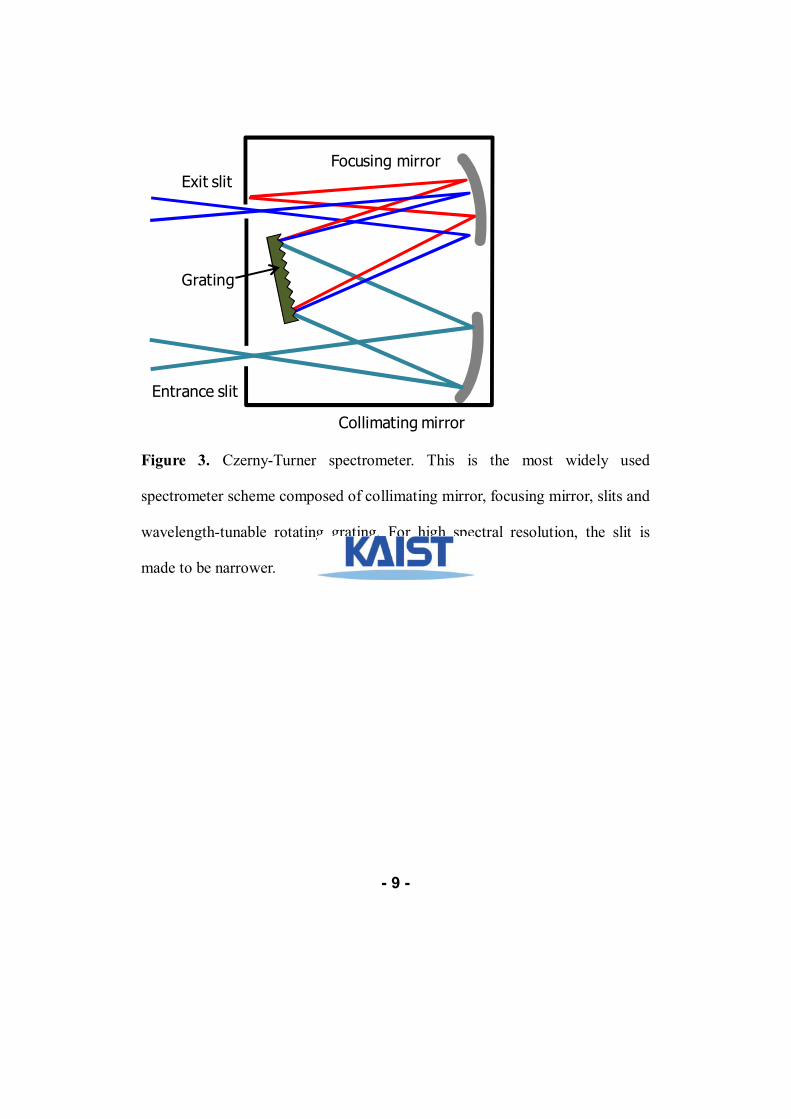
compared to the conventional spectrometers. Figure 3 shows the most widely
used scheme of Czerny-Turner spectrometer. In the common Czerny-Turner
design, the broad band illumination source is aimed at an entrance slit. The
amount of light energy available for use depends on the intensity of the source
in the space defined by the slit (width * height) and the acceptance angle of the
optical system. The slit is placed at the effective focus of a collimating mirror
so that the light from the slit reflected from the mirror is collimated (focused at
infinity). The collimated light is refracted by the prism or diffracted from the
grating and then is collected by another focusing mirror which refocuses the
light, now dispersed, on the exit slit. At the exit slit, the colors of the light are
spread. Because each color arrives at a separate point in the exit slit plane,
there are a series of images of the entrance slit focused on the plane. Because
the entrance slit is finite in width, parts of nearby images overlap. The light
leaving the exit slit contains the entire image of the entrance slit of the selected
color plus parts of the entrance slit images of nearby colors. A rotation of the
dispersing element causes the band of colors to move relative to the exit slit, so
that the desired entrance slit image is centered on the exit slit. The range of

- 8 -
colors leaving the exit slit is a function of the width of the slits. The entrance
and exit slit widths are adjusted together.
For direct spectrometric analysis, diffraction component have been
integrated in LOC. Hollow prism uses air mirrors mentioned above and shows
low spectral resolution. Micro lens and grating assembly[25-28] is
miniaturizing setups of conventional spectrometer and has a deep sample
chamber of about 5 mm vertically which is not usual in microfluidic devices.
Optical path in the vertical direction would be worse in getting uniform optical
path length if compared to that in the microfluidic channel direction. Therefore,
reproducible absorbance analysis with high sensitivity and resolution can be
achieved if microfluidic sample channel, optical path extension and the
spectrometric analysis happen in the same planar direction.
For planar integration of optical elements such as grating, slits, mirrors and
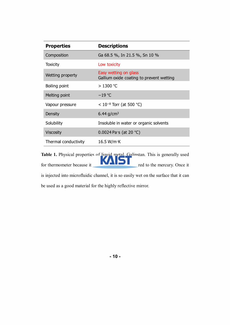
lenses, this paper proposes liquid metal material. Table 1 shows the physical
properties of liquid metal, galinstan which is widely used for thermometer
because of low toxicity. Once it is injected into microfluidic channel, it is so
easily we on the surface of PDMS and glass, that it can be used as a good
material for the highly reflective mirror.
- 9 -
Figure 3. Czerny-Turner spectrometer. This is the most widely used
spectrometer scheme composed of collimating mirror, focusing mirror, slits and
wavelength-tunable rotating grating. For high spectral resolution, the slit is
made to be narrower.
Collimating mirror
Focusing mirror
Entrance slit
Exit slit
Grating
- 10 -
Table 1. Physical properties of liquid metal, Galinstan. This is generally used
for thermometer because it is very low toxic compared to the mercury. Once it
is injected into microfluidic channel, it is so easily wet on the surface that it can
be used as a good material for the highly reflective mirror.
Properties Descriptions
Composition Ga 68.5 %, In 21.5 %, Sn 10 %
Toxicity Low toxicity
Wetting propertyEasy wetting on glassGallium oxide coating to prevent wetting
Boiling point > 1300 °C
Melting point −19 °C
Vapour pressure < 10−8 Torr (at 500 °C)
Density 6.44 g/cm3
Solubility Insoluble in water or organic solvents
Viscosity 0.0024 Pa·s (at 20 °C)
Thermal conductivity 16.5 W/m·K

- 11 -
1.2. Research objectives
This paper uses liquid metal mirrors for multiple internal reflections in a
microfluidic device to extend the optical path length. Extended optical path
length is expected to make high sensitivity and low limit of detection with low
optical loss and highly effective light focusing. With various incident angles of
20°, 30°, 40° and 50°, optical path extension is effectively save the size of the
lab chips.
For simple spectrometric analysis using optical fibers, a new novel
platform is proposed. Liquid metal is used to make optical components such as
lenses, mirrors and slits. Diffraction element of transmissive grating is
fabricated using SU-8 mold and PDMS peel-off. It is integrated into
microfluidic device with planar focusing lens embedded. Output spectrum is
demonstrated with 3 optical fibers of 50 ㎛ core, 150 ㎛ cladding and 250
㎛ coating. They are centered to measure 400 nm, 500 nm and 600 nm
respectively.
- 12 -
Chapter 2. Materials and methods
2.1. Chip design
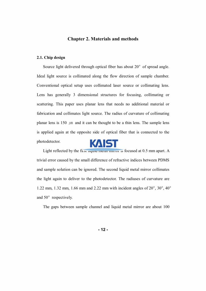
Source light delivered through optical fiber has about 20° of spread angle.
Ideal light source is collimated along the flow direction of sample chamber.
Conventional optical setup uses collimated laser source or collimating lens.
Lens has generally 3 dimensional structures for focusing, collimating or
scattering. This paper uses planar lens that needs no additional material or
fabrication and collimates light source. The radius of curvature of collimating
planar lens is 150 ㎛ and it can be thought to be a thin lens. The sample lens
is applied again at the opposite side of optical fiber that is connected to the
photodetector.
Light reflected by the first liquid metal mirror is focused at 0.5 mm apart. A
trivial error caused by the small difference of refractive indices between PDMS
and sample solution can be ignored. The second liquid metal mirror collimates
the light again to deliver to the photodetector. The radiuses of curvature are
1.22 mm, 1.32 mm, 1.66 mm and 2.22 mm with incident angles of 20°, 30°, 40°
and 50° respectively.
The gaps between sample channel and liquid metal mirror are about 100

- 13 -
㎛ which is relatively narrow compared to the height of the microfluidic
channel, 250 ㎛. If sample solution and liquid metal is not handled by syringe
pumps, channel walls tend to break down or the curvature is distorted easily.
The purpose of this device is to measure absorbance for analyzing the
concentration of the solution. Figure 4 shows the chip design and the
connections. Optical path extension is achieved longer as the incident angle
lowers. 4 kinds of incident angles are applied, 20°, 30°, 40° and 50°. To focus
the light better, planar lenses are integrated where the sample channel and
optical fibers meet as explained above. Optical path length is designed to be 3
mm equally to know the absorbance measurements change as the incident
angles change. If the incident angle does not affect the reflectance of liquid
metal mirrors, optical path can be extended longer with the same size of sample
chamber in a microfluidic device. Moreover, scattered light through sample
chamber can be focused to enhance the signal to noise ratio.
Optical fiber cannot be reassembled to the device, but since the end of
optical fiber is configured as commercial SMA block, various kinds of lasers,
LEDs and photodetectors can be used at the same device. As the color of
sample changes, the combination of light source and detector should change
too. If sample chamber is washed, the device can be reused many times.

- 14 -
Figure 4. Chip design for optical path extension using liquid metal mirrors.
Optical fibers are connected to light source and photodetector. Optical path
length is 3 mm with various incident angles of 20°, 30°, 40° and 50°.
Photodetector signal includes noise that would be calibrated with averaging
method. The noise is measured to calculate the standard deviation.
455 nm LED
time
Liquid metal
Sample
Inte
nsi
ty
Sample detected
Optical fiber
Optical fiber

- 15 -
The purpose of the second device is spectrometric analysis using optical
components made by liquid metal channels. A new platform using liquid metal
and PDMS grating measures absorbance spectrometric response. All optical
components such as thin planar lens, optical fibers, slits and transmissive
grating are integrated in planar direction and the liquid metal is used to make
entrance slit of light. This scheme is directly adapted to the lab chips which
automatically handle samples. Absorbance meter is integrated into one simple
lab chip. Figure 5 shows the chip design of the spectrometer and the
connections. It is composed of light source, avalanche photodetector(APD),
optical fibers, sample chamber, liquid metal slit and elastomeric grating.
Elastomeric grating has 100 grooves per 1 mm. Distance between grating
patterns is 10 ㎛ with 30° of blaze angle. Mold is composed of SU-8
photoresistor which is the most commonly used for soft lithography. Since the
height of mold is 250 ㎛, aspect ratio is about 25:1. To avoid complicated
fabrication process, the grating pattern of align mask is an array of rectangular
blocks with width of 2 ㎛ and length of 10 ㎛. The gap between rectangular
blocks is 10 ㎛. The energy of UV exposure was 260 mJ/cm2.
Since the shape of sample chamber ends sharply, light tends to be focused
at the front of the liquid metal slit. The difference of refractive indices between

- 16 -
sample solution and PDMS induces total internal reflection and liquid metal
mirror reflects the refracted light. It is thought to be helpful to enhance the
effectiveness of absorbance detection.
The gap between two liquid metal channels is 10 ㎛ which can be reduced
to 2 ㎛ with high pressure into liquid metal channels. Since liquid metal never
allows for light to pass through, it is a perfect material for optical slit. Because
of sharp shape of slit, bubbles are easily generated. Too much pressure to
remove bubble can destroy the wall between liquid metal channels.
Light that passed through slit is collimated by planar thin lens. If it’s not
collimated, spectral resolution becomes hard to predict. Diffracted light by
transmissive grating is reflected by liquid metal mirror. The purpose of this
mirror is to enhance spectral resolution in a small area of device for detection
by optical fibers. The radiuses of curvature of planar thin lens and liquid metal
mirror is 120 ㎛, 110 ㎛ respectively.

- 17 -
Figure 5. Chip design for spectrometric analysis. Optical fibers are connected
to light source and photodetectors. Detection wavelength are centered at 400
nm, 500 nm, 600 nm respectively. Optical path length is 3 mm and the light
passing liquid metal slit is collimated by planar lens and diffracted by the
PDMS integrated transmissive grating of 100 grooves/mm. For higher spectral
resolution, the diffracted light is reflected by liquid metal.
1 mm
White LED
GB R
Liquid metal
Sample
- 18 -
2.2. Fabrication process
A new device platform using liquid metal to extend optical path in
microfluidic channel direction is suggested. Table 1 shows the property of
liquid metal, Galinstan. It has a high reflectivity and easily wetting property. It
acts as liquid in room temperature and doesn’t solid over -19°C. Incident angle
doesn’t have to consider the critical angle that is convenient to extend optical
path effectively and we demonstrated incident angles of 20°, 30°, 40° and 50°.
For comparisons to air mirror devices, the same device can be used if liquid
metal is not injected. Linear channel with the same optical path length has been
used for comparison too.
The devices have been fabricated by casting of PDMS (Sylgard 184
elastomer kit, Dow Corning, Midland, MI, USA) in an SU-8 master
(MicroChem, Corp., Newton, MA, USA). The technology is extremely simple
and it has been deeply studied and reported, nevertheless, for completeness it is
reproduced here. After informal cleaning and dehydrating a 0.5 mm thick
Boron doped Si wafer at 175°C for 20 minutes, the substrate is spin-coated
with 250 ㎛ of a SU-8 layer at 2500 rpm for 30 seconds. Afterwards, the
substrates are baked at 65°C and 95°C for 7 and 45 minutes respectively and
exposed to UV light of 350 mJ/cm2 with a mask. The post-exposure bake (PEB)
- 19 -
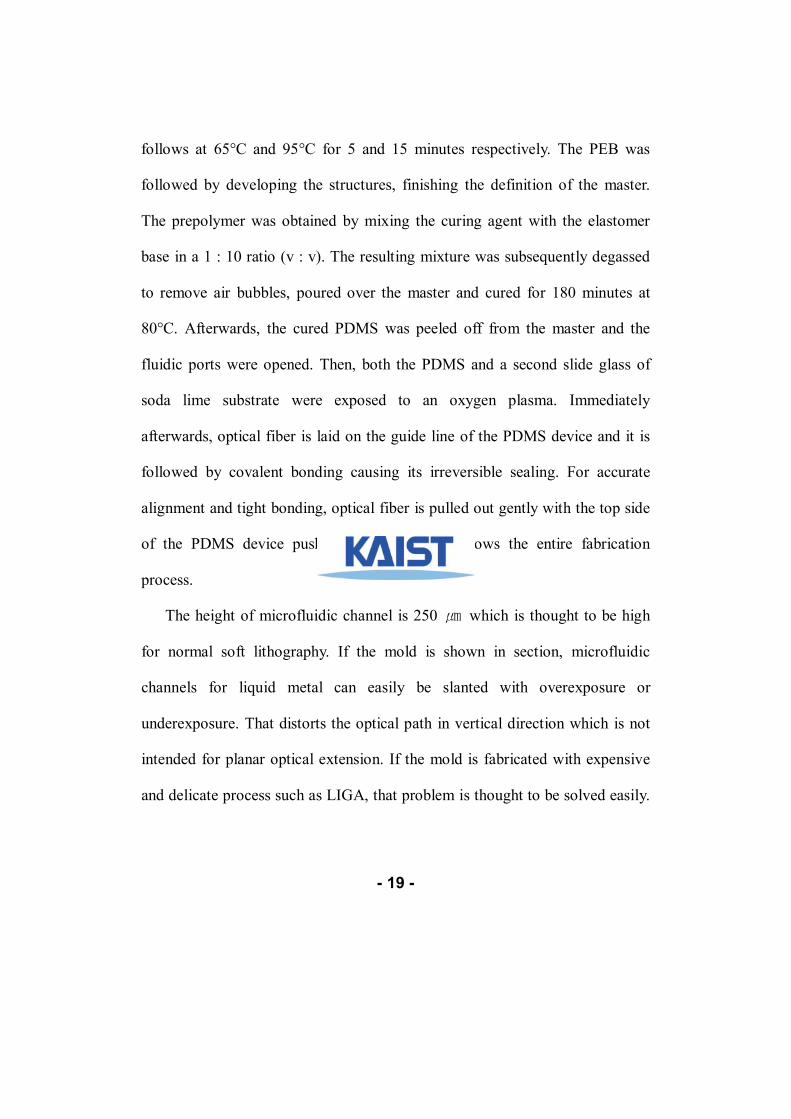
follows at 65°C and 95°C for 5 and 15 minutes respectively. The PEB was
followed by developing the structures, finishing the definition of the master.
The prepolymer was obtained by mixing the curing agent with the elastomer
base in a 1 : 10 ratio (v : v). The resulting mixture was subsequently degassed
to remove air bubbles, poured over the master and cured for 180 minutes at
80°C. Afterwards, the cured PDMS was peeled off from the master and the
fluidic ports were opened. Then, both the PDMS and a second slide glass of
soda lime substrate were exposed to an oxygen plasma. Immediately
afterwards, optical fiber is laid on the guide line of the PDMS device and it is
followed by covalent bonding causing its irreversible sealing. For accurate
alignment and tight bonding, optical fiber is pulled out gently with the top side
of the PDMS device pushed down. Figure 6 shows the entire fabrication
process.
The height of microfluidic channel is 250 ㎛ which is thought to be high
for normal soft lithography. If the mold is shown in section, microfluidic
channels for liquid metal can easily be slanted with overexposure or
underexposure. That distorts the optical path in vertical direction which is not
intended for planar optical extension. If the mold is fabricated with expensive
and delicate process such as LIGA, that problem is thought to be solved easily.

- 20 -
With just simple tuning of exposure condition, no expensive lithography is
needed. Si wafer scatters UV source at the bottom side of the mold and top side
of mold is always exposed the most. It causes shape of mold to be a lens and
focuses light to the center of vertical direction. To avoid cracks along the
channel walls, PEB is done once more with low temperature, 60°C for 4 hours.
- 21 -
Figure 6. Fabrication process. The entire softlithography is illustrated. For
accurate alignment and tight bonding between optical fibers and PDMS device,
optical fiber is pulled out slowly and PDMS device is pushed down.
PDMS
Making a mold(H = 250 ㎛)
H
Curing PDMS
SU-8
Si
Inserting optical fiberinto PDMS device
Optical fiber
Si
Plasma bondingto slide glass
Slide glass
Pulling out optical fiberslowly for tight bonding
Slide glass
- 22 -
2.3. Experimental setup
For testing the optical path extension, fluorescence dye of fluorecein is
used. Fluorescein is a fluorophore commonly used in microscopy, in a type of
dye laser as the gain medium, in forensics and serology to detect latent blood
stains, and in dye tracing. Fluorescein has an absorption maximum at 494 nm
and emission maximum of 521 nm (in water). Fluorescein also has an
isosbestic point (equal absorption for all pH values) at 460 nm. Fluorescein
sodium is used extensively as a diagnostic tool in the field of ophthalmology
and optometry, where topical fluorescein is used in the diagnosis of corneal
abrasions, corneal ulcers and herpetic corneal infections. It is also used in rigid
gas permeable contact lens fitting to evaluate the tear layer under the lens.
Intravenous or oral fluorescein is used in fluorescein angiography in research
and to diagnose and categorize vascular disorders in e.g. legs, including retinal
disease macular degeneration, diabetic retinopathy, inflammatory intraocular
conditions, and intraocular tumors , and increasingly during surgery for brain
tumors. In cellular biology, the isothiocyanate derivative of fluorescein is often
used to label and track cells in fluorescence microscopy applications (for
example, flow cytometry). Additional biologically active molecules (such as
antibodies) may also be attached to fluorescein, allowing biologists to target
- 23 -
the fluorophore to specific proteins or structures within cells. This application
is common in yeast display. Fluorescein can also be conjugated to nucleoside
triphosphates and incorporated into a probe for in situ hybridisation.
Fluorescein-labelled probes can be imaged using FISH, or targeted by
antibodies using immunohistochemistry. The latter is a common alternative to
digoxigenin, and the two are used together for labelling two genes in one
sample.
For testing the spectrometer, trypan blue and phenol red are used. Trypan
blue is commonly used in microscopy (for cell counting) and in laboratory
mice for assessment of tissue viability. The method cannot distinguish between
necrotic and apoptotic cells. Most living tissues prosper at a near-neutral pH;
that is, a pH close to 7. The pH of blood ranges from 7.35 to 7.45, for instance.
When cells are grown in tissue culture, the medium in which they grow is held
close to this physiological pH. A small amount of phenol red added to this
growth medium will have a pink-red color under normal conditions. Typically
15 mg / 1 L is used for cell culture. In the event of problems, waste products
produced by dying cells or overgrowth of contaminants will cause a change in
pH, leading to a change in indicator color. For example, a culture of relatively
slowly-dividing mammalian cells can be quickly overgrown by bacterial

- 24 -
contamination. This usually results in an acidification of the medium, turning it
yellow. Many biologists find this a convenient way to rapidly check on the
health of tissue cultures. In addition, the waste products produced by the
mammalian cells themselves will slowly decrease the pH, gradually turning the
solution orange and then yellow. This color change is an indication that even in
the absence of contamination, the medium needs to be replaced (generally, this
should be done before the medium has turned completely orange). Since the
color of phenol red can interfere with some spectrophotometric and fluorescent
assays, many types of tissue culture media are also available without phenol
red.
Light source is precisely controlled by constant current driver (Thorlabs).
MPPC is used for highly sensitive photo-detection. White LED is turned on
with 350 mA of constant current. Bundle software provided by Hamamatsu is
used to control and acquire signal from MPPC. Shutter speed and exposure
time are configurable. The signal is captured for 5 seconds after 30 seconds of
warming up of LED. Table 2 shows the list of materials for experimental setups.
- 25 -
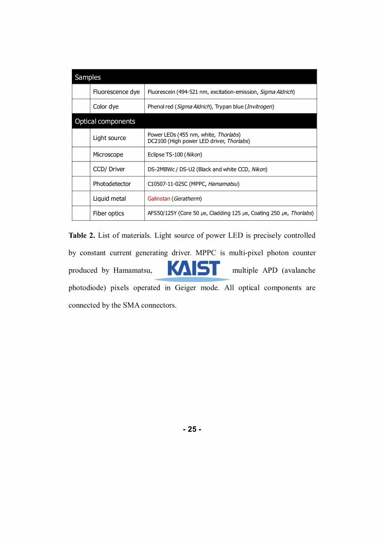
Table 2. List of materials. Light source of power LED is precisely controlled
by constant current generating driver. MPPC is multi-pixel photon counter
produced by Hamamatsu, which is made up of multiple APD (avalanche
photodiode) pixels operated in Geiger mode. All optical components are
connected by the SMA connectors.
Samples
Fluorescence dye Fluorescein (494-521 nm, excitation-emission, Sigma Aldrich)
Color dye Phenol red (Sigma Aldrich), Trypan blue (Invitrogen)
Optical components
Light sourcePower LEDs (455 nm, white, Thorlabs)DC2100 (High power LED driver, Thorlabs)
Microscope Eclipse TS-100 (Nikon)
CCD/ Driver DS-2MBWc / DS-U2 (Black and white CCD, Nikon)
Photodetector C10507-11-025C (MPPC, Hamamatsu)
Liquid metal Galinstan (Geratherm)
Fiber optics AFS50/125Y (Core 50 ㎛, Cladding 125 ㎛, Coating 250 ㎛, Thorlabs)
- 26 -
2.4. Evaluation criteria
The most generally accepted quantitative definition of detection limit is that
it is the minimum concentration or mass of analyte that can be detected at a
known confidence level. This limit depends upon the ratio of the magnitude of
the analytical signal to the size of the statistical fluctuations in the blank signal.
That is, unless the analytical signal is larger than the blank by some multiple k
of the variation in the blank owing to random errors, it is impossible to detect
the analytical signal with certainty. Thus, as the limit of detection is
approached, the analytical signal and its standard deviation approach the blank
signal and its standard deviation. The minimum distinguishable analytical
signal is then taken as the sum of the mean blank signal plus a multiple k of the
standard deviation of the blank. The resulting data are then treated statistically
to obtain mean blank signal and its standard deviation. Recommended value of
k is 3. Figure 7 shows the equations of LOD[29] and sensitivity[30].
The quantitative definition of sensitivity that is accepted by the
International Union of Pure and Applied Chemists (IUPAC) is calibration
sensitivity, which is the slope of the calibration curve at the concentration of
interest. A disadvantage of analytical sensitivity is that it is often concentration
dependent since standard deviation of sensor varies with concentration.

- 27 -
Figure 7. Definition of limit of detection (LOD) and sensitivity. LOD is
generally used 3 times of standard deviation of blank signal devided by slopt of
the straight line. Sensitivities vary as the concentration of solution varies. In
this paper, sensitivity means the minimum sensitivity of the measured
absorbance.
Limit of Detection (LOD)* =3 blanks
m
×
Sensitivity** =s
m
s
: slope of the straight line: standard deviation of the blank signal: standard deviation of the measurement
mblanks
ss
Abso
rban
ce (
-lo
g (
I 1/I 0
) )
Concentrationblanks
mSlope =

- 28 -
Chapter 3. Results and discussions
3.1. Optical path extension
The optical path extension has been accomplished with small angle of
incidence, 20° without trade-offs of sensitivity and LOD. Table 3 shows the
microscope imaging comparisons liquid metal mirrors to air mirrors and linear
channel. No additional device is fabricated for comparison test to air mirror.
Liquid metal mirror works as air mirror if liquid metal channel is not filled
with anything. Air mirror doesn’t reflect incident angles below 45° of critical
angle but liquid metal mirror works good with lower optical loss. The working
principle of liquid metal mirror is basically different from the air mirror which
is based on the difference of refractive indices between materials. The
molecular structure of liquid metal is dense like other metals in liquid status
which enables reflect light with high efficiency. Generally speaking, metals
reflect light with their own colors, but liquid metal, galinstan distorts the color
of incident light much less than other metal materials. Since liquid metal mirror
doesn’t have to consider incident angle, multiple internal reflections have been
done successfully with small incident angle, 20° and smaller angle is expected
to be adapted, too. If incident angle becomes lower than 5°, optical path can be

- 29 -
extended very longer in a narrow sample chamber. It can be used to detect
single droplet to sort by the number of cells trapped. For simple comparisons,
linear channel is designed to be a rectangular shape, and it would work better if
it’s been a sharpening shape in outlet direction. Since that kind of design
includes other design considerations, it’s not applied here.
Figure 8 shows the comparisons of LODs and sensitivities, which says the
enhancements of liquid metal mirrors. It is caused by the focusing of incident
light which results lower optical loss by scattering. In the concentration range
under 500 nM, the absorbance measured more in detail to compare the LOD
calculated and graph which match well. Even though optical loss in air mirror
is relatively higher, LOD and sensitivity of air mirror is almost the same as
these of linear channel. Liquid metal mirror has better performance compared
to the air mirror and linear channel. With the absorbance detection using 5 μM
of fluorecein, LOD becomes 4.5 times lower from 377 nM to 84 nM and
sensitivity becomes 3.6 times higher from 1.29x10⁻³ to 3.62x10⁻⁴.
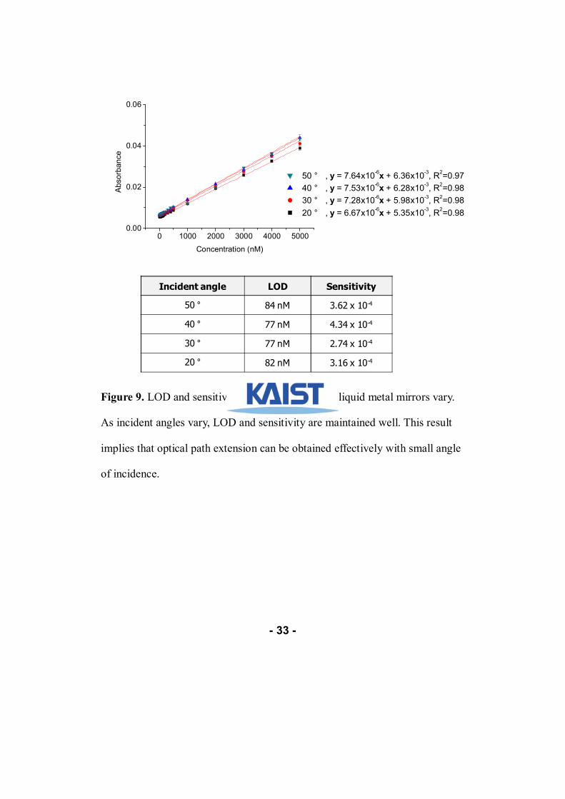
As the incident angle lowers, optical path can be extended more effective.
Various incident angles of 20°, 30°, 40° and 50° are tested and figure 9 shows
there is no trade-offs of LODs and sensitivities with incident angles. It means
the performance is maintained if optical path is extended with small angle of
- 30 -
incidence. Since incidence angle can be lowered below 20°, this feature can be
adapted to various applications.
Liquid metal mirrors can be designed flexibly to focus or collimate light.
For absorbance measurement in a microfluidic device, there is a strong need to
minimize the size of the conventional flowcells of optical path length from
several mm to several hundreds of mm. The purpose of flowcell is to detect
small number of concentrations by absorbance detection in a long linear
sample chamber. The sample should be delivered from other container that
results sample loss and risk of contaminations. Since there’s no additional
focusing element in linear shape of flowcells, sensitivity and LOD cannot be
enhanced. A new novel platform of optical path extension using liquid metal
mirrors consumes small sample volume directly from sample chamber in a
microfluidic device, and enhances LOD and sensitivity with lower optical loss
than linear channel or air mirror.

- 31 -
Inci
dent
angle
20 °
30 °
40 °
50 °
Liq
uid
m
eta
l m
irro
r
Air
mirro
r
Linear
channel
1 m
m1 m
m
1 m
m
1 m
m1 m
m1 m
m1 m
m
1 m
m1 m
m
* Solu
tion :
5 μ
Mof fluore
scein
Light
sourc
e : 4
55 n
m p
ow
er LE
D @
350 m
A
Ta
ble
3. C
om
par
iso
ns li
qu
id m
etal
mir
rors
to a
ir m
irro
rs a
nd
lin
ear
chan
nel
. Air
mir
rors
do
no
t ref
lect
inci
den
t lig
ht w
hen
inci
den
t an
gle
is b
elo
w 4
5 °
, cri
tica
l an
gle
.
Bu
t liq
uid
met
al m
irro
rs re
flec
t an
d f
ocu
s in
cid
ent l
igh
t wel
l.

- 32 -
Figure 8. Liquid metal mirrors type compared to linear channel and air mirrors
type. Liquid metal mirrors collect scattered light better causing lower LOD and
higher sensitivity.
0 1000 2000 3000 4000 50000.00
0.02
0.04
0.06
0.08A
bso
rba
nce
Concentration (nM)
Linear channel, y = 5.67x10⁻⁶ x + 3.82x10
-2, R
2 = 0.93
Air mirror, y = 6.17x10⁻⁶ x + 2.20x10
-2, R
2 = 0.98
Liquid metal mirror, y = 7.64x10⁻⁶ x + 6.36x10
-3, R
2 = 0.97
Type LOD Sensitivity
Linear channel 377 nM 1.29 x 10⁻³
Air mirrors 225 nM 1.10 x 10⁻³
Liquid metal mirrors 84 nM 3.62 x 10⁻⁴
- 33 -
Figure 9. LOD and sensitivity as incident angles of liquid metal mirrors vary.
As incident angles vary, LOD and sensitivity are maintained well. This result
implies that optical path extension can be obtained effectively with small angle
of incidence.
0 1000 2000 3000 4000 50000.00
0.02
0.04
0.06
Ab
sorb
an
ce
Concentration (nM)
50 ° , y = 7.64x10⁻⁶x + 6.36x10
-3, R
2=0.97
40 ° , y = 7.53x10⁻⁶x + 6.28x10
-3, R
2=0.98
30 ° , y = 7.28x10⁻⁶x + 5.98x10
-3, R
2=0.98
20 ° , y = 6.67x10⁻⁶x + 5.35x10
-3, R
2=0.98
Incident angle LOD Sensitivity
50 ° 84 nM 3.62 x 10⁻⁴
40 ° 77 nM 4.34 x 10⁻⁴
30 ° 77 nM 2.74 x 10⁻⁴
20 ° 82 nM 3.16 x 10⁻⁴

- 34 -
3.2. Spectrometer
The gaps between optical fibers for R,G,B measurements are 350 ㎛
respectively. This new design of spectrometer provides a detailed spectral
resolution, but it is limited by optical fiber setup. This platform is useful for the
applications to measure profile of color using optical fibers. The core size of
optical fibers is 50 ㎛, so it is the same as the 50 ㎛ of optical fibers arranged
in the gaps of 350 ㎛. The tests are to know the feasibility for measurements of
profile of solution color and absorbance change as concentrations vary. LOD
and sensitivity are calculated after measurements too.
Solutions of different colors, phenol red and trypan blue are used to
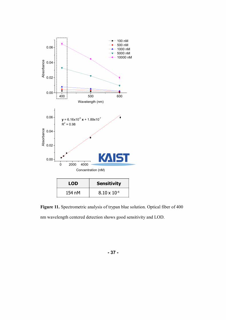
demonstrate the spectrometer using liquid metal. Figure 10 shows the result of
the absorbance measurement of phenol red from 3 optical fibers that are
centered to measure 400 nm, 500 nm and 600 nm respectively. Then red fiber
of 600 nm is plotted with 212 nM of LOD and 1.09x10⁻³ of sensitivity. Figure
11 shows the result of the absorbance measurement of trypan blue from 3
optical fibers too. Then blue fiber of 400 nm is plotted with 154 nM of LOD
and 8.10x10⁻⁴ of sensitivity. For optical fiber using applications, this platform
is very simple and effective for spectral analysis. As two figures show, profiles
of colors from solutions of different colors express absolutely different. The

- 35 -
maximum absorbance has happened in optical fiber aligned to red color
measuring phenol red and blue color measuring trypan blue as expected. White
LED is thought to be a disadvantage to reduce the performance of LOD and
sensitivity, but it proved that the spectral resolution is high enough. Profile of
colors measured can be developed to know the kinds and concentrations of
sample solutions.
Comparisons to previous researches are shown in table 4. This scheme is
closer to the structure of conventional spectrometer and optical components of
mirrors, lenses and slits are fabricated simply just by microfluidic channel and
liquid metal. Hollow prism is simple for fabrication compared to the
transmissive grating integration with trade-off of spectral resolution. In planar
optical path extension, optical components such as optical fibers and
photodetectors are essential. If optical fiber is used, simply measurement by
microscope is impossible. This novel design of device performs well with
simple optical configuration. This platform is available for both of
concentration measurement of known solution and analyzing unknown material
in solution status.

- 36 -
Figure 10. Spectrometric analysis of phenol red solution. Optical fiber of 600
nm wavelength centered detection shows good sensitivity and LOD.
400 500 6000.00
0.02
0.04
0.06A
bso
rba
nce
Wavelength (nm)
100 nM 500 nM 1000 nM 5000 nM 10000 nM
0 2000 4000 6000 8000 10000
0.00
0.02
0.04
0.06 y = 3.67x10⁻⁶ x + 1.21x10
-3
R2 = 0.98
Ab
so
rba
nce
Concentration (nM)
LOD Sensitivity
212 nM 1.09 x 10⁻³
- 37 -
Figure 11. Spectrometric analysis of trypan blue solution. Optical fiber of 400
nm wavelength centered detection shows good sensitivity and LOD.
400 500 6000.00
0.02
0.04
0.06
Ab
sorb
ance
Wavelength (nm)
100 nM 500 nM 1000 nM 5000 nM 10000 nM
0 2000 4000 6000 8000 10000
0.00
0.02
0.04
0.06y = 6.16x10
-6 x + 1.89x10
-7
R2 = 0.98
Abso
rban
ce
Concentration (nM)
LOD Sensitivity
154 nM 8.10 x 10⁻⁴

- 38 -
Fig
ure
Diffract
ion
ele
ment
Optica
lto
ol
Weak
poin
tFa
brica
tion
difficu
lty
Transm
issive
PD
MS
gra
ting
Optica
l fiber
-N
orm
al
(Gra
ting
pat
tern
)
Hollo
w p
rism
Optica
l fiber
Low
reflect
ive
air m
irro
r Easy
Com
merc
ial
transm
issive
gra
ting
Mic
rosc
ope
Colli
mating
lens
Hard
(U
nusu
ally
deep
sam
ple
cham
ber)
Ta
ble
4. C
om
par
iso
ns to
oth
er s
pec
tro
met
ers.
Ho
llo
w p
rism
usi
ng
air
mir
ror h
as
low
refl
ecti
vit
y ca
usi
ng
op
tica
l lo
ss. C
om
mer
cial
tran
smis
siv
e g
rati
ng
typ
e h
as
un
usu
ally
dee
p s
amp
le c
ham
ber
an
d b
ad q
ual
ity
of c
oll
imat
ing
len
s.

- 39 -
Chapter 4. Conclusion
4.1. Summary
Liquid metal mirrors can be designed with minimum optical loss and
incident angle, which makes the size of the lab chip smaller. Conventional
flowcells that are used to measure absorbance are expected to be substituted by
the design of multiple internal reflections. Liquid metal can be used as optical
components materials such as mirror, slit, lens. Just by simple design of
microfluidic channel and liquid metal injection, optical path are manipulated to
focus, scatter and be blocked. High reflectivity of liquid metal mirrors results
the enhancements of LOD and sensitivity, 4.5 times and 3.6 times respectively,
compared to the air mirrors and linear channel. There is no trade-offs of LOD
and sensitivity as the incident angle lowers.
A new platform for spectrometer analysis on lab chips have been developed
using liquid metal. By simple design of microfluidic device and liquid metal
material injection, spectrometer close to conventional device scheme has been
achieved with high LOD and sensitivity.

- 40 -
4.2. Further works
Previous works using liquid metal in a microfluidic device are about
electrowetting property and applications related to liquid metal of droplet
manipulations[31,32]. Liquid metal requires high potential for electrowetting
and can be handled within expected range of wetting property, so handling
liquid metal in a microfluidic device is not a big deal. Using this property,
optical path extension in vertical direction can be made for imaging by
microscopy or CCD like figure 12 (a) shows. If device is well assembled with
light source and photodetector, a lab chip can be expected to be integrated with
user friendly design.
Optical fiber that has been used as waveguide in this paper too purposes to
carry light with minimized optical loss[33]. Since optical fibers cannot be
integrated every time in restricted area, waveguide like figure 12 (b) can be
made to focus light in planar directions. Just like planar lens which is now
commonly used, we expect planar waveguide using liquid metal be the solution
for focusing light in a microfluidic device.
Figure 12 (c) shows a good example of single droplet analysis. Single
droplet can be sorted and analyzed with absorbance detection which varies
with number of cells that contains. Light with small incident angle can be

- 41 -
captured with small sample volume, high sensitivity and low LOD without
conventional long flowcells. When minimum available design of incident angle
is applied, small concentration of single droplet can be analyzed without design
change of sample chambers. Droplet measurement and sorting technique by
optical properties are not well developed yet compared to the manipulation
techniques. This idea is expected to suggest a new common platform for design
of droplet detection.
This paper presented two schemes for absorbance detection which are
multiple internal reflections by liquid metal mirrors and spectrometric analysis
using liquid metal slit and mirrors. If they are combined in a device, figure 13
is a good example. As the test reports of liquid metal mirrors say here, optical
properties such as LOD and sensitivity are expected to be enhanced a lot if two
of them are combined in a microfluidic device.
Liquid metal as a new material for optical components to integrate in a lab
chip can be applied to many other applications. Absorbance and other optical
properties can be found to be enhanced with developments of liquid metal
components.

- 42 -
Figure 12. Various applications for further works. (a) shows the optical path
extension in vertical direction using electrowetting property of liquid metal. (b)
shows focusing light with minimum optical loss in planar direction. (c) shows
multiple internal reflections with small incident angle to detect single droplet.
(a)
(b)
(c)
Fiber optics Focused light

- 43 -
Figure 13. Optical path extension combined to spectrometric analysis. (a)
shows the scheme for transmissive grating and (b) is for reflective grating.
Liquid metal mirrors
Sample channelFiber optics connected to detectors
Fiber optics connected to light sources
Biconvex lenses
Transmissive grating
Liquid metal slits
a
Reflective liquid metal grating
b
- 44 -
Summary in Korean
본 에 미 체 내 체 거울 한 경
(optical path extension)과 학 (spectrometric analysis) 할
수 새 운 태 스에 한 연 수행하 다. 체
거울 LED 빛 사 량 시료
한 량 집 할 수 다. 경 한 스 20°,
30°, 40°, 50° 다 한 각도 사각에 하여 실험 수행하 다.
행 연 공 거울 식과 채 과 비 하 고,
비 지 감지 (Limit of detection, LOD) 감도
(sensitivity) 비 하 다. 체 거울 한 스 사각
지 라도 감지 감도 실 생하지 고,
수에 한 fluorescein 도 측 하 사각 50°
감지 84 nM, 감도 3.62x10⁻⁴ 얻 수 었
다. 다 스 스 트 미 미 체 시료채 평
향에 경 하여 측 할 수 새
운 플랫폼 다. 생 학시료 에 많 쓰 phenol
red trypan blue 하여 스 트럼 수행하 , 감지
감도가 각각 212 nM, 154 nM, 1.09x10⁻³, 8.10x10⁻⁴ 한
수행할 수 하 다.
- 45 -
References
[1] Younan Xia, and George M. Whitesides, “Soft lithography,” Angew.
Chem. Int. Ed. Engl., 37, pp. 551-575, 1998
[2] Vijay Srinivasan, Vamsee K. Pamula, and Richard B. Fair, “An
integrated digital microfluidic lab-on-a-chip for clinical diagnostics on
human physiological fluids,” Lab Chip, 4, pp. 310-315, 2004
[3] G. Minas, J. S. Martins, and J. H. Correia, “High-selectivity optical
detection in microfluidic systems for clinical diagnostics,” The 14th
European conference on Solid-State Transducers, pp. 873-876, 2000
[4] Wen-Bin Du, Qun Fnag, Qiao-Hong He, and Zhao-Lun Fang, “High-
throughput nanoliter sample introduction microfluidic chip-based flow
injection analysis system with gravity-driven flows,” Anal. Chem., 77,
pp. 1330-1337, 2005
[5] Frances S. Ligler, “Perspective on optical biosensors and integrated
sensor systems,” Anal. Chem., 81, pp. 519-526, 2009
[6] Helen Waechter, Klaus Bescherer, Christoph J. Durr, Richard D.
Oleschuk, and Hans-Peter Loock, “405 nm absorption detection in
nanoliter volumes,” Anal. Chem., 81, pp. 9048-9051, 2009
[7] Demetri Psaltis, Stephen R. Quake, and Changhuei Yang, “Developing
- 46 -
optofluidic technology through the fusion of microfluidics and optics,”
Nature, 442, pp. 381-386, 2006
[8] Albert van den Berg, and T. S. J. Lammerink, “Micro total analysis
systems: Microfluidic aspects, integration concept and applications,”
Current Chemistry, 194, pp. 21-49, 1998
[9] Steven A. Soper, Kathlynn Brown, Andrew Ellington, Bruno Frazier,
Guillermo Garcia-Manero, Vincent Gauf, Steven I. Gutman, Daniel F.
Hayes, Brenda Korte, James L. Landers, Dale Larson, Frances Ligler,
Arun Majumdar, Marco Mascini, David Nolte, Zeev Rosenzweig,
JosephWang, and David Wilson, “Point-of-care biosensor systems for
cancer diagnostics/prognostics,” Biosens. Bioelec., 21, pp. 1932-1942,
2006
[10] Adam Bange, H. Brian Halsall, and William R. Heineman,
“ Microfluidic immunosensor systems,” Biosens. Bioelec., 20, pp.
2488-2503, 2005
[11] Anja Gulliksen, Lars Anders Solli, Klaus Stefan Drese, Olaf Sorensen,
Frank Karlsen, Henrik Rogne, Eivind Hovig, and Reidun Sirevag
“Parallel nanoliter detection of cancer markers using polymer
microchips,” Lab Chip, 5, pp. 416-420, 2005

- 47 -
[12] Avraham Rasooly, and James Jacobson, “Development of biosensors
for cancer clinical testing,” Biosens. Bioelec., 21, pp. 1851-1858, 2006
[13] Jie Wu, Zhifeng Fu, Feng Yan, and Huangxian Ju, “Biomedical and
clinical applications of immunoassays and immunosensors for tuor
markers,” Anal. Chem., 26, pp. 679-688, 2007
[14] Winny Tan, Leyla Sabet, Yang Li, Tianwei Yu, Perry R. Klokkevold,
David T. Wong, and Chih-Ming Ho, “Optical protein sensor for
detecting cancer markers in saliva,” Biosens. Bioelec., 24, pp. 266-271,
2008
[15] Paul Yager, Thayne Edwards, Elain Fu, Kristen Helton, Kjell Nelson,
Milton R. Tam, and Bernhard H. Weigl, “Microfluidic diagnostic
technologies for global public health,” Nature, 442, pp. 412-418, 2006
[16] Jeonggi Seo, and Luke P. Lee, “Disposable integrated microfluidics
with self-aligned planar microlenses,” Sens. Actuators B Chem., 99, pp.
615-622, 2004
[17] Frank B. Myers, and Luke P. Lee, “Innovations in optical microfluidic
technologies for point-of-care diagnostics,” Lab Chip, 8, pp. 2015-2031,
2008
[18] A. Llobera, R. Wilke, and S. Buttgenbach, “Enhancement of the

- 48 -
response of poly(dimethylsiloxane) hollw pisms through air mirrors for
absorbance-based sensing,” Talanta, 75, pp. 473-479, 2008
[19] A. Llobera, S. Demming, R. Wilke and S. Buttgenbach, “Multiple
internal reflection poly(dimethylsiloxane) systems for optical sensing,”
Lab chip, 7, pp. 1560-1566, 2007
[20] Hossein Salimi-Moosavi, Yutao Jiang, Lianne Lester, Graham
McKinnon, and D. Jed Harrison, “A multireflection cell for enhanced
absorbance detection in microchip-based capillary electrophoresis
devices,” Eletrophoresis, 21, pp. 1291-1299, 2000
[21] J. D. J. Ingle, and S. R. Crouch, “Spectrochemical analysis”, Prentice
Hall, New Jersey, 1988
[22] J. Steigert, M. Grumann, T. Brenner, L. Riegger, J. Harter, R. Zengerle,
and J. Ducree, “Fully integrated whole blood testing by real-time
absorption measurement on a centrifugal platform,” Lab chip, 6, 1040-
1044, 2006
[23] Toshihiko Noda, Hidekuni Takao, Kazunori Yoshioka, Narihiro Oku,
Mitsuaki Ashiki, Kazuaki Sawada, Koichi Matsumoto, Makoto Ishida,
“Performance of absorption photometry microchip for blood
hemoglobin measurement integrated with processing circuits and

- 49 -
Si(110) 45◦ mirrors,” Sens. Actuators B Chem., 119, pp. 245-250, 2006
[24] Sungyoung Choi, Je-Kyun Park, "Optically coated mirror-embedded
microchannel to measure hydrophoretic particle ordering in three
dimensions," Small, 5, pp. 2205-2211, 2009
[25] Nicolae Damean, Samuel K. Sia, Vincent Linder, Max Narovlyansky,
and George M. Whitesides, “Space- and time-resolved
spectrophotometry in Microsystems,” Proc. Natl. Acad. Sci., 102, pp.
10035-10039, 2005
[26] James L. Wilbur, Rebecca J. Jackman, and George M. Whitesides,
“Elastomeric Optics,” Chem Master., 8, pp. 1380-1385, 1996
[27] Dominique Bourgeois, Xavier Vernede, Virgile Adam, Emanuela
Fioravanti, and Thomas Ursby, “A Microspectrophotometer for UV-
visible absorption and fluorescence studies of protein crystals,”, J. Appl.
Cryst., 35, pp. 319-326, 2002
[28] J. B. McManus, P. L. Kebabian, and M. S. Zahniser, “Astigmatic mirror
multipass absorption cells for long-path-length spectroscopy,” Appl.
Optics, 34, pp. 3336-3348 , 1995
[29] David J. Anderson, and Jack L. Rudy, “Determination of the lower limit
of detection,” Clin. Chem., 35, pp. 2152-2153, 1989

- 50 -
[30] John Mandel, “Estimation of weighting factors in linear regression and
analysis of variance,” Nat Bur. Stand., 6, pp. 1-25, 2964
[31] Zhiliang Wan, Hongjun Zeng, and Alan Feinerman, “Area-tunable
micromirror based on electrowetting actuation of liquid-metal droplets,”
Appl.Phys. Lett., 89, pp. 201107, 2006
[32] Uriel Levy, and Romi Shamai, “Tunable optofluidic devices,”
Microfluid Nanofluid, 4, pp. 97-105, 2008
[33] Jack Sheng Kee, Daniel Puiu Poenar, Pavel Neuzil, and Levent Yobas,
“Monolithic integration of poly(dimethylsiloxane) waveguides and
microfluidics for on-chip absorbance measurements,” Sens. Actuators B
Chem., 134, pp. 532-538, 2008


![Reporte Tecnologia Planar[1]](https://img.pdfslide.tips/doc/110x75/557210c2497959fc0b8da447/reporte-tecnologia-planar1.jpg)