Embed Size (px)
Citation preview

DescriptionThe A3921 is a full-bridge controller for use with external N-channel power MOSFETs and is specifically designed for automotive applications with high-power inductive loads, such as brush DC motors.
A unique charge pump regulator provides full (>10 V) gate drive for battery voltages down to 7 V and allows the A3921 to operate with a reduced gate drive, down to 5.5 V.
A bootstrap capacitor is used to provide the above-battery supply voltage required for N-channel MOSFETs. An internal charge pump for the high-side drive allows DC (100% duty cycle) operation.
The full bridge can be driven in fast or slow decay modes using diode or synchronous rectification. In the slow decay mode, current recirculation can be through the high-side or the low-side FETs. The power FETs are protected from shoot-through by resistor adjustable dead time.
Integrated diagnostics provide indication of undervoltage, overtemperature, and power bridge faults, and can be configured to protect the power MOSFETs under most short circuit conditions.
The A3921 is supplied in a 28-pin TSSOP power package with an exposed thermal pad (suffix LP). This package is lead (Pb) free, with 100% matte-tin leadframe plating.
3921-DS
Features and Benefits▪ High current gate drive for N-channel MOSFET full bridge▪ High-side or low-side PWM switching▪ Charge pump for low supply voltage operation▪ Top-off charge pump for 100% PWM▪ Cross-conduction protection with adjustable dead time▪ 5.5 to 50 V supply voltage range▪ Integrated 5 V regulator▪ Diagnostics output▪ Low current sleep mode
Automotive Full Bridge MOSFET Driver
Package: 28-pin TSSOP with exposed thermal pad (suffix LP)
Typical Application
Not to scale
A3921
A3921
VBAT
PWM
Direction
Fault Flags

Automotive Full Bridge MOSFET DriverA3921
2Allegro MicroSystems, LLC115 Northeast CutoffWorcester, Massachusetts 01615-0036 U.S.A.1.508.853.5000; www.allegromicro.com
Selection GuidePart Number Packing
A3921KLPTR-T 4000 pieces per reel
THERMAL CHARACTERISTICS may require derating at maximum conditionsCharacteristic Symbol Test Conditions* Value Units
Package Thermal ResistanceRθJA
4-layer PCB based on JEDEC standard 28 ºC/W
2-layer PCB with 3.8 in.2 of copper area each side 32 ºC/W
RθJP 2 ºC/W
*Additional thermal information available on Allegro website.
Absolute Maximum Ratings*Characteristic Symbol Notes Rating Units
Load Supply Voltage VBB –0.3 to 50 V
Logic Inputs and Outputs –0.3 to 6.5 V
V5 Pin –0.3 to 7 V
LSS Pin –4 to 6.5 V
VDSTH Pin –0.3 to 6.5 V
SA and SB Pins –5 to 55 V
VDRAIN Pin –5 to 55 V
GHA and GHB Pins Sx to Sx+15 V
GLA and GLB Pins –5 to 16 V
CA and CB Pins –0.3 to Sx+15 V
Operating Temperature Range TA Range K –40 to 150 ºC
Junction Temperature TJ(max) 150 ºC
Transient Junction Temperature TtJ
Overtemperature event not exceeding 1 s, lifetime duration not exceeding 10 hr; guaranteed by design characterization
175 ºC
Storage Temperature Range Tstg –55 to 150 ºC
*With respect to GND.
Automotive Full Bridge MOSFET DriverA3921
3Allegro MicroSystems, LLC115 Northeast CutoffWorcester, Massachusetts 01615-0036 U.S.A.1.508.853.5000; www.allegromicro.com
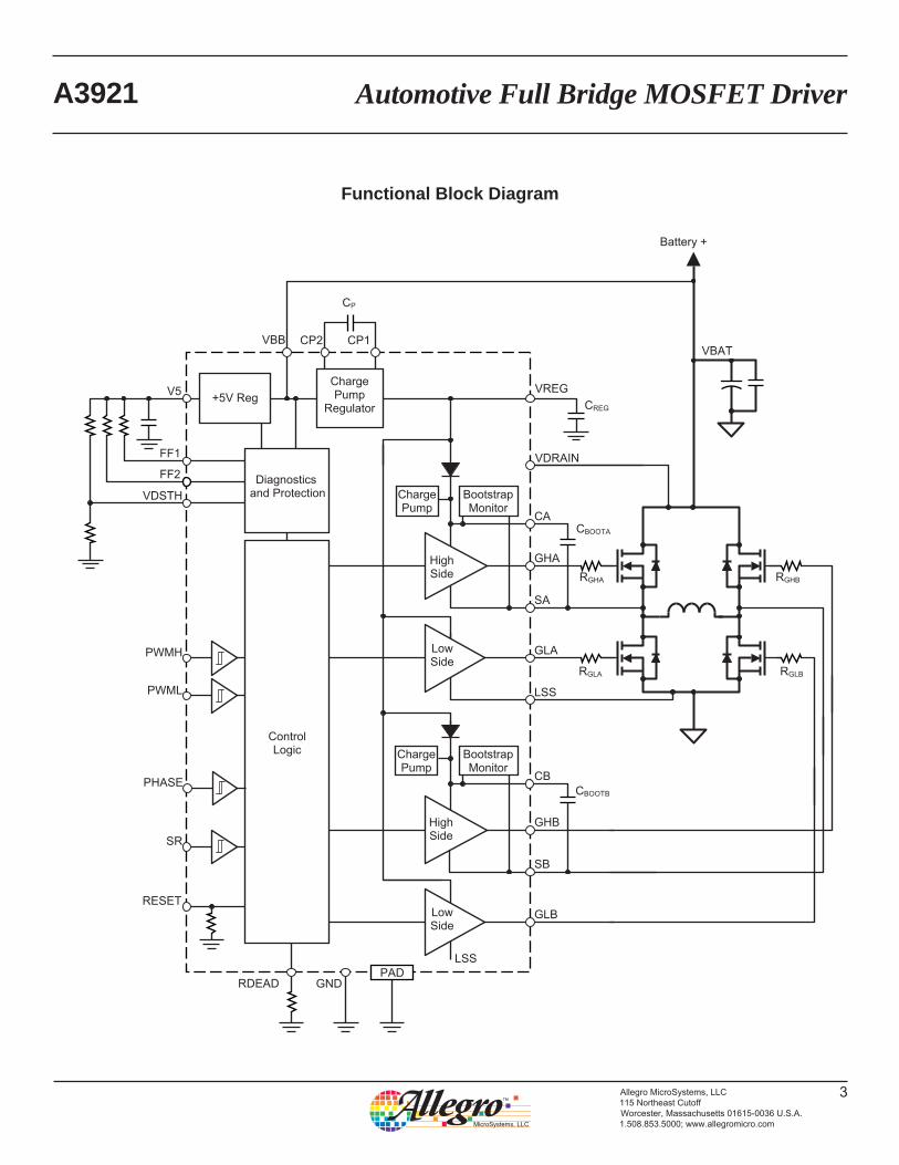
Functional Block Diagram
ChargePump
Regulator
ControlLogic
+5V Reg
Diagnostics and Protection
VBATCP1CP2
SR
FF2
LSS
GLA
GHA
SA
CA
VREG
Battery +
PHASE
VBB
V5
RGHA
RGLA
CBOOTA
CREG
CP
PWML
PWMH
RDEAD
VDSTH
VDRAIN
RESET
FF1
ChargePump
BootstrapMonitor
Low Side
GLB
GHB
SB
CB
RGHB
RGLB
CBOOTB
ChargePump
BootstrapMonitor
HighSide
Low Side
LSS
HighSide
GNDPAD

Automotive Full Bridge MOSFET DriverA3921
4Allegro MicroSystems, LLC115 Northeast CutoffWorcester, Massachusetts 01615-0036 U.S.A.1.508.853.5000; www.allegromicro.com
Characteristics Symbol Test Conditions Min. Typ. Max. UnitsSupply and ReferenceLoad Supply Voltage Functional Operating Range1 VBB 5.5 – 50 V
Load Supply Quiescent CurrentIBBQ RESET = high, outputs = low, VBB = 12 V – 10 14 mA
IBBS RESET = low, Sleep mode, VBB = 12 V – – 10 μA
VREG Output Voltage VREG
VBB > 9 V, IREG = 0 to 10 mA 12.5 13 13.75 V
7.5 V < VBB ≤ 9 V, IREG = 0 to 7 mA 12.5 13 13.75 V
6 V < VBB ≤ 7.5 V, IREG = 0 to 7 mA 2×VBB – 2.5 – – V
5.5 V < VBB ≤ 6 V, IREG < 5.5 mA 8.5 9.5 – V
V5 Output Voltage V5(out) No load 4.5 5 5.5 V
V5 Line Regulation V5(line) I5 = –2 mA – 15 40 mV
V5 Load Regulation V5(load) I5 = 0 to –2 mA – 50 100 mV
V5 Short-Circuit Current I5M VBB = 40 V, V5 = 0 V – 28 35 mA
Bootstrap Diode Forward Voltage VfBOOTID = 10 mA 0.4 0.7 1.0 V
ID = 100 mA 1.5 2.2 2.8 V
Bootstrap Diode Resistance rDrD(100mA) = (VfBOOT(150mA) – VfBOOT(50mA)) / 100 mA 6 10 20 Ω
Bootstrap Diode Current Limit IDBOOT 250 500 750 mA
Top-off Charge Pump Current Limit ITOCPM – 400 – μA
High-Side Gate Drive Static Load Resistance RGSH 250 – – kΩ
Gate Output DriveTurn-On Time tr CLOAD = 1 nF, 20% to 80% – 35 – ns
Turn-Off Time tf CLOAD = 1 nF, 80% to 20% – 20 – ns
Pullup On Resistance RDS(on)UPTJ = 25°C, IGHx = –150 mA 6 8 12 Ω
TJ = 150°C, IGHx = –150 mA 10 13 16 Ω
Pulldown On Resistance RDS(on)DNTJ = 25°C, IGLx = 150 mA 2 3 4 Ω
TJ = 150°C, IGLx = 150 mA 3 4.5 6 Ω
GHx Output Voltage VGHX Bootstrap capacitor fully charged VCx – 0.2 – – V
GLx Output Voltage VGLXVREG – 0.2 – – V
Turn-Off Propagation Delay2 tP(off)Input change to unloaded gate output change 60 90 150 ns
Turn-On Propagation Delay2 tP(on)Input change to unloaded gate output change 60 90 150 ns
Propagation Delay Matching, Phase-to-Phase ∆tPPMeasured between corresponding transition points on both phases – 10 – ns
Propagation Delay Matching, On-to-Off ∆tOO Measured across one phase – 10 – ns
ELECTRICAL CHARACTERISTICS valid at TJ = –40°C to 150°C, VBB = 7 to 50 V, unless noted otherwise
Continued on the next page…

Automotive Full Bridge MOSFET DriverA3921
5Allegro MicroSystems, LLC115 Northeast CutoffWorcester, Massachusetts 01615-0036 U.S.A.1.508.853.5000; www.allegromicro.com
Characteristics Symbol Test Conditions Min. Typ. Max. UnitsGate Output Drive (continued)
Dead Time2 tDEAD
RDEAD = 3 kΩ – 180 – ns
RDEAD = 30 kΩ 815 960 1110 ns
RDEAD = 240 kΩ – 3.5 – μs
RDEAD tied to V5 – 6 – μs
Logic Inputs and OutputsFF1 and FF2 Fault Output (Open Drain) VFF(L) IFF = 1 mA, fault not present – – 0.4 V
FF1 and FF2 Fault Output Leakage Current3 IFF(H) VFF = 5 V, fault present –1 – 1 μA
RDEAD Current3 IDEAD RDEAD = GND –200 – –70 μA
Input Low Voltage VIN(L) – – 0.8 V
Input High Voltage VIN(H) 2.0 – – V
Input Hysteresis (Except RESET Pin) VINhys 100 250 – mV
Input Hysteresis (RESET Pin) VINRSThys 200 – – mV
Input Current (Except RESET Pin)3 IIN 0 V < VIN < V5 –1 – 1 μA
Input Pulldown Resistor (RESET Pin) RPD – 50 – kΩ
RESET Pulse Time tRES 0.1 – 3.5 μs
Protection
VREG Undervoltage Lockout ThresholdVREGUVon VREG rising 7.5 8 8.5 V
VREGUVoff VREG falling 6.75 7.25 7.75 V
Bootstrap Undervoltage Threshold VBOOTUV Cx with respect to Sx 59 – 69 %VREG
Bootstrap Undervoltage Hysteresis VBOOTUVhys – 13 – %VREG
V5 Undervoltage Turn-Off Threshold V5UVoff V5 falling 3.4 3.6 3.8 V
V5 Undervoltage Hysteresis V5UVhys 300 400 500 mV
VDSTH Input Range VDSTH 0.1 – 2 V
VDSTH Input Current IDSTH 0 V < VDSTH < 2 V – 10 30 μA
VDSTH Disable Voltage VDSDIS When not connected directly to V5 4.95 – – V
VDRAIN Input Voltage VDRAIN VDSTH = 2 V, VBB = 12 V, 7 VBB 50 V
VDRAIN Input Current IDRAINVDSTH = 2 V, VBB = 12 V, 0 V < VDRAIN < VBB
– – 250 μA
Short-to-Ground Threshold Offset4 VSTGOHigh-side on, VDSTH ≥ 1 V – ±100 – mV
High-side on, VDSTH < 1 V –150 ±50 150 mV
Short-to-Battery Threshold Offset5 VSTBOLow-side on, VDSTH ≥ 1 V – ±100 – mV
Low-side on, VDSTH < 1 V –150 ±50 150 mV
Overtemperature Fault Flag Threshold TJF Temperature increasing 150 170 – ºC
Overtemperature Fault Hysteresis TJFhys Recovery = TJF – TJFhys – 15 – ºC1Functions correctly, but parameters are not guaranteed, below the general limits (7 V).2See Gate Drive Timing diagrams.3For input and output current specifications, negative current is defined as coming out of (sourcing) the specified device pin.4As VSx decreases, fault occurs if VBAT –VSx > VSTG. STG threshold, VSTG = VDSTH + VSTGO .5As VSx increases, fault occurs if VSx – VLSS > VSTB . STB threshold, VSTB = VDSTH+VSTBO .
ELECTRICAL CHARACTERISTICS (continued) valid at TJ = –40°C to 150°C, VBB = 7 to 50 V, unless noted otherwise
Automotive Full Bridge MOSFET DriverA3921
6Allegro MicroSystems, LLC115 Northeast CutoffWorcester, Massachusetts 01615-0036 U.S.A.1.508.853.5000; www.allegromicro.com
PHASE
GLA
GHA
tDEAD tDEAD
tP(off) tP(off)
PWML=1, PWMH=1
GHB
GLB
PWMH
GLA
GHAtP(off) tP(on)
PHASE=1
GHB
GLB
PWML
PWMH
GLx
GHx
tP(off) tP(on)
SR=0, PWML=1
PWML
GLx
GHx
tP(on)tP(off)
SR=0, PWMH=1
PWMH
GLx
GHx
tDEAD tDEAD
tP(off) tP(off)
SR=1, PWML=1
PWML
GLx
GHx
tDEAD
tP(off)
tDEAD
tP(off)
SR=1, PWMH=1
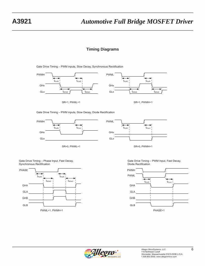
Timing Diagrams
Gate Drive Timing – PWM inputs, Slow Decay, Synchronous Rectification
Gate Drive Timing – PWM inputs, Slow Decay, Diode Rectification
Gate Drive Timing – Phase Input, Fast Decay,Synchronous Rectification
Gate Drive Timing – PWM Input, Fast Decay,Diode Rectification

Automotive Full Bridge MOSFET DriverA3921
7Allegro MicroSystems, LLC115 Northeast CutoffWorcester, Massachusetts 01615-0036 U.S.A.1.508.853.5000; www.allegromicro.com
The A3921 is a full-bridge MOSFET driver (pre-driver) requiring a single unregulated supply of 7 to 50 V. It includes an integrated 5 V logic supply regulator.
The four high current gate drives are capable of driving a wide range of N-channel power MOSFETs, and are configured as two high-side drives and two low-side drives. The A3921 provides all the necessary circuits to ensure that the gate-source voltage of both high-side and low-side external FETs are above 10 V, at supply voltages down to 7 V. For extreme battery voltage drop conditions, correct functional operation is guaranteed at supply voltages down to 5.5 V, but with a reduced gate drive voltage.
The A3921 can be driven with a single PWM input from a microcontroller and can be configured for fast or slow decay. Fast decay can provide four-quadrant motor control, while slow decay is suitable for two-quadrant motor control or simple induc-tive loads. In slow decay, current recirculation can be through the high-side or the low-side MOSFETs. In either case, bridge efficiency can be enhanced by synchronous rectification. Cross-conduction (shoot through) in the external bridge is avoided by an adjustable dead time.
A low power sleep mode allows the A3921, the power bridge, and the load to remain connected to a vehicle battery supply without the need for an additional supply switch.
The A3921 includes a number of protection features against undervoltage, overtemperature, and power bridge faults. Fault states enable responses by the device or by the external control-ler, depending on the fault condition and logic settings. Two fault flag outputs, FF1 and FF2, are provided to signal detected faults to an external controller.
Power Supplies
A single power supply connection is required to the VBB pin through a reverse voltage protection circuit. The supply should be decoupled with a ceramic capacitor connected close to the VBB and ground pins.
The A3921 operates within specified parameters with a VBB supply from 7 to 50 V and functions correctly with a supply down to 5.5 V. This provides a very rugged solution for use in the harsh automotive environment.
V5 Pin A 5 V low current supply for external pullup resistors is provided by an integrated 5 V regulator. This regulator is also
used by the internal logic circuits and must always be decoupled by at least a 100 nF capacitor between the V5 pin and GND. The 5 V regulator is disabled when RESET is held low.
Gate Drives
The A3921 is designed to drive external, low on-resistance, power N-channel MOSFETs. It supplies the large transient cur-rents necessary to quickly charge and discharge the external FET gate capacitance in order to reduce dissipation in the external FET during switching. The charge and discharge rate can be controlled using an external resistor in series with the connection to the gate of the FET.
Gate Drive Voltage Regulation The gate drives are powered by an internal regulator which limits the supply to the drives and therefore the maximum gate voltage. When the VBB supply is greater than about 16 V, the regulator is a simple linear regulator. Below 16 V, the regulated supply is maintained by a charge pump boost converter, which requires a pump capacitor connected between the CP1 and CP2 pins. This capacitor must have a mini-mum value of 220 nF, and is typically 470 nF.
The regulated voltage, nominally 13 V, is available on the VREG pin. A sufficiently large storage capacitor must be connected to this pin to provide the transient charging current to the low-side drives and the bootstrap capacitors.
Top-off Charge Pump An additional top-off charge pump is provided for each phase. The charge pumps allow the high-side drives to maintain the gate voltage on the external FETs indefi-nitely, ensuring so-called 100% PWM if required. This is a low current trickle charge pump, and is operated only after a high-side FET has been signaled to turn on. The floating high-side gate drive requires a small bias current (<20 μA) to maintain the high-level output. Without the top-off charge pump, this bias current would be drawn from the bootstrap capacitor through the Cx pin. The charge pump provides sufficient current to ensure that the bootstrap voltage and thereby the gate-source voltage is main-tained at the necessary level.
Note that the charge required for initial turn-on of the high-side gate is always supplied by the bootstrap capacitor. If the bootstrap capacitor becomes discharged, the top-off charge pump will not provide sufficient current to allow the FET to turn on.
Functional Description

Automotive Full Bridge MOSFET DriverA3921
8Allegro MicroSystems, LLC115 Northeast CutoffWorcester, Massachusetts 01615-0036 U.S.A.1.508.853.5000; www.allegromicro.com
In some applications a safety resistor is added between the gate and source of each FET in the bridge. When a high-side FET is held in the on-state, the current through the associated high-side gate-source resistor (RGSH) is provided by the high-side drive and therefore appears as a static resistive load on the top-off charge pump. The minimum value of RGSH for which the top-off charge pump can provide current is shown in the Electrical Characteris-tics table.
GLA and GLB Pins These are the low-side gate drive outputs for the external N-channel MOSFETs. External resistors between the gate drive output and the gate connection to the FET (as close as possible to the FET) can be used to control the slew rate seen at the gate, thereby providing some control of the di/dt and dv/dt of the SA and SB outputs. GLx going high turns on the upper half of the drive, sourcing current to the gate of the low-side FET in the external power bridge, turning it on. GLx going low turns on the lower half of the drive, sinking current from the external FET gate circuit to the LSS pin, turning off the FET.
SA and SB Pins Directly connected to the motor, these terminals sense the voltages switched across the load. These terminals are also connected to the negative side of the bootstrap capacitors and are the negative supply connections for the floating high-side drives. The discharge current from the high-side FET gate capaci-tance flows through these connections, which should have low impedance circuit connections to the FET bridge.
GHA and GHB Pins These terminals are the high-side gate drive outputs for the external N-channel FETs. External resistors between the gate drive output and the gate connection to the FET (as close as possible to the FET) can be used to control the slew rate seen at the gate, thereby controlling the di/dt and dv/dt of the SA and SB outputs. GHx going high turns on the upper half of the drive, sourcing current to the gate of the high-side FET in the external motor-driving bridge, turning it on. GHx going low turns on the lower half of the drive, sinking current from the external FET gate circuit to the corresponding Sx pin, turning off the FET.
CA and CB Pins These are the high-side connections for the bootstrap capacitors and are the positive supply for the high-side gate drives. The bootstrap capacitors are charged to approxi-mately VREG when the associated output Sx terminal is low. When the Sx output swings high, the charge on the bootstrap capacitor causes the voltage at the corresponding Cx terminal to rise with the output to provide the boosted gate voltage needed for the high-side FETs.
LSS Pin This is the low-side return path for discharge of the capacitance on the FET gates. It should be tied directly to the common sources of the low-side external FETs through an inde-pendent low impedance connection.
RDEAD Pin This pin controls internal generation of dead time during FET switching.
• When a resistor greater than 3 kΩ is connected between RDEAD and AGND, cross-conduction is prevented by the gate drive circuits, which introduce a dead time, tDEAD , between switching one FET off and the complementary FET on. The dead time is derived from the resistor value connected between the RDEAD and AGND pins.
• When RDEAD is connected directly to V5, cross-conduction is prevented by the gate drive circuits. In this case, tDEAD defaults to a value of 6 μs typical.
Logic Control Inputs
Four low-voltage level digital inputs provide control for the gate drives. These logic inputs all have a nominal hysteresis of 500 mV to improve noise performance. They are used together to provide fast decay or slow decay with high-side or low-side recirculation. They also provide brake, coast, and sleep modes as defined in tables 1 and 2.
PWMH and PWML Pins These inputs can be used to control current in the power bridge. PWMH provides high-side chopping and PWML provides low-side chopping. When used together they control the power bridge in fast decay mode. The PWM options are provided in table 2.
• Setting PWMH low turns off active high-side drives. This provides high-side–chopped slow-decay PWM.
• Setting PWML low turns off active low-side drives. This provides low-side–chopped slow-decay PWM.
• PWMH and PWML may also be connected together and driven with a single PWM signal. This provides fast-decay PWM.
PHASE Pin The state of the PHASE pin determines the positive direction of load current (see table 1). The PHASE pin can also be used as a PWM input when full four-quadrant control (fast decay synchronous rectification) is required (see table 2).
SR Pin This enables or disables synchronous rectification. When SR is high, synchronous rectification is enabled during the PWM off time. PWM off time is present when there is a low on either

Automotive Full Bridge MOSFET DriverA3921
9Allegro MicroSystems, LLC115 Northeast CutoffWorcester, Massachusetts 01615-0036 U.S.A.1.508.853.5000; www.allegromicro.com
Table 1. Phase Control Truth TableInputs Outputs Bridge
Mode of OperationPWMH PWML PHASE SR GHA GLA GHB GLB SA SB
1 1 1 X H L L H HS LS Bridge driven with A high and B low
1 1 0 X L H H L LS HS Bridge driven with B high and A low
0 1 X 1 L H L H LS LS Slow decay, both low-side on or low-side brake
1 0 X 1 H L H L HS HS Slow decay, both high-side on or high-side brake
0 1 1 0 L L L H Z LS Slow decay, current flow A to B, low-side diode rectification
0 1 0 0 L H L L LS Z Slow decay, current flow B to A, low-side diode rectification
1 0 1 0 H L L L HS Z Slow decay, current flow A to B, high-side diode rectification
1 0 0 0 L L H L Z HS Slow decay, current flow B to A, high-side diode rectification
0 0 X X L L L L Z Z Fast decay, diode rectification/coast
X = don’t care (same for input 1 or input 0), HS = high-side FET active, LS = low-side FET active, Z = high impedance, both FETs off
Table 2. PWM OptionsInputsa PWM Effectb
Decay Mode of OperationSR PWMH PWML PHASE 100% 0%X 1 1 PWM A to B B to A Fast Full four-quadrant control, zero average load current at 50% PWM
0 PWM PWM1 A to B
Coast Fast Fast decay, diode recirculation or coast0 B to A
1 PWM 11 A to B
Brake Slow High-side PWM, low-side MOSFET recirculation0 B to A
1 1 PWM1 A to B
Brake Slow Low-side PWM, high-side MOSFET recirculation0 B to A
0 PWM 11 A to B
Brakec Slow High-side PWM, low-side diode recirculation0 B to A
0 1 PWM1 A to B
Brakec Slow Low-side PWM, high-side diode recirculation0 B to A
X 0 0 X Coast Coast Fast Coast, all MOSFETs offaX indicates don’t care condition. The action is the same for input 1 or input 0.bPWM Effect indicates the effect on the load current direction or the equivalent action.cWith SR disabled, braking is only effective in one direction when sufficient forward voltage is available to allow the diode to conduct.

Automotive Full Bridge MOSFET DriverA3921
10Allegro MicroSystems, LLC115 Northeast CutoffWorcester, Massachusetts 01615-0036 U.S.A.1.508.853.5000; www.allegromicro.com
but not both of the PWMH and PWML inputs. Synchronous rectification turns on the complementary MOSFET to the one that is turned off. This ensures that the recirculating current passes through the lower resistance conduction path, rather than the body diode of the MOSFET.
When SR is low, synchronous rectification is disabled. In this case, fewer MOSFET switching cycles occur, reducing dissipa-tion in the A3921. However, load current recirculates through the higher resistance body diode of the power MOSFETs, causing greater power dissipation in the power bridge.
RESET Pin This is an active-low input, and when active it allows the A3921 to enter sleep mode. When RESET is held low, the regulator and all internal circuitry are disabled and the A3921 enters sleep mode. Before fully entering sleep mode, there is a short delay while the regulator decoupling and storage capacitors discharge. This typically takes a few milliseconds, depending on the application conditions and component values.
During sleep mode, current consumption from the VBB supply is reduced to a minimal level. In addition, latched faults and the corresponding fault flags are cleared. When the A3921 is coming out of sleep mode, the protection logic ensures that the gate drive outputs are off until the charge pump reaches its correct operat-ing condition. The charge pump stabilizes in approximately 3 ms under nominal conditions.
RESET can be used also to clear latched fault flags without entering sleep mode. To do so, hold RESET low for less then the reset pulse time, tRES. This clears any latched fault that disables the outputs, such as short circuit detection or bootstrap capacitor undervoltage.
Note that the A3921 can be configured to start without any exter-nal logic input. To do so, pull up the RESET pin to VBB by means of an external resistor. The resistor value should be between 20 and 33 kΩ.
Coast and Brake States
To put the power bridge into a coast state, that is all power bridge MOSFETs switched off, the two PWM inputs, PWMH and PWML, must be held low and at the same time SR must be held low. This forces all gate drive outputs low.
Braking is achieved by forcing the power bridge to apply a short across the load, allowing the back EMF of the load to generate a braking torque.
Several brake states are possible using combinations of inputs on PWMH, PWML, and SR. For example, holding PWML and SR high, while PWMH is low, turns on both low-side FETs to short the load. The shorting path is always present and provides braking in both directions of motor rotation. Another example is holding SR low, when PWML is high and PWMH is low, mak-ing only one low-side FET active, and the braking current flow through the body diode of the opposite low-side FET. This pro-vides braking in only one direction, because the diode does not permit the braking current to flow if the motor is reversed. Also, the braking current can be made to circulate around the high-side switches by swapping PWMH and PWML.
Diagnostics
Several diagnostic features are integrated into the A3921 to provide indication of fault conditions and, if required, take action to prevent permanent damage. In addition to system-wide faults such as undervoltage and overtemperature, the A3921 integrates individual drain-source monitors for each external FET, to pro-vide short circuit detection.
Diagnostic Management Pins
VDSTH Pin Faults on the external FETs are determined by measuring the drain-source voltage, VDS , of each active FET and comparing it to the threshold voltage applied to the VDSTH input, VDSTH. To avoid false fault detection during switching transients, the comparison is delayed by an internal blanking timer. If the voltage applied to the VDSTH pin is greater than the disable threshold voltage, VDSDIS , then FET short circuit detec-tion is disabled.
VDRAIN Pin This is a low current sense input from the top of the external FET bridge. This input allows accurate measurement of the voltage at the drain of the high-side FETs. It should be con-nected directly to the common connection point for the drains of the power bridge FETs at the positive supply connection point. The input current to the VDRAIN pin is proportional to the volt-age on the VDSTH pin and can be approximated by:
IVDRAIN = 72 × VDSTH + 52 ,
where IVDRAIN is the current into the VDRAIN pin, in μA, and VDSTH is the voltage on the VDSTH pin, in V.
FF1 and FF2 Pins These are open drain output fault flags, which indicate fault conditions by their state, as shown in table 3. In

Automotive Full Bridge MOSFET DriverA3921
11Allegro MicroSystems, LLC115 Northeast CutoffWorcester, Massachusetts 01615-0036 U.S.A.1.508.853.5000; www.allegromicro.com
the event that two or more faults are detected simultaneously, the state of the fault flags will be determined by a logical OR of the flag states for all detected faults.
Table 3. Fault DefinitionsFlag State
Fault Description Disable Outputs*
Fault LatchedFF1 FF2
Low Low No fault No –
Low High Short-to-ground Yes Yes
Low High Short-to-supply Yes Yes
Low High Shorted load Yes Yes
High Low Overtemperature No No
High High V5 undervoltage Yes No
High High VREG undervoltage Yes No
High High Bootstrap undervoltage Yes Yes
*Yes indicates all gate drives low, and all FETs off.
Fault States
Overtemperature If the junction temperature exceeds the over-temperature threshold, typically 165°C, the A3921 will enter the overtemperature fault state and FF1 will go high. The overtem-perature fault state, and FF1, will only be cleared when the tem-perature drops below the recovery level defined by TJF – TJFhys .
No circuitry will be disabled. External control circuits must take action to limit the power dissipation in some way so as to prevent overtemperature damage to the A3921 chip and unpredictable device operation.
VREG Undervoltage VREG supplies the low-side gate driver and the bootstrap charge current. It is critical to ensure that the voltages are sufficiently high before enabling any of the outputs. If the voltage at VREG, VREG , drops below the falling VREG undervoltage lockout threshold, VREGUVoff , then the A3921 will enter the VREG undervoltage fault state. In this fault state, both FF1 and FF2 will be high, and the outputs will be disabled. The VREG undervoltage fault state and the fault flags will be cleared when VREG rises above the rising VREG undervoltage lockout threshold, VREGUVon.
The VREG undervoltage monitor circuit is active during power-up, and the A3921 remains in the VREG undervoltage fault state until VREG is greater than the rising VREG undervolt-age lockout threshold, VREGUVon.
Bootstrap Capacitor Undervoltage The A3921 monitors the voltage across the individual bootstrap capacitors to ensure they have sufficient charge to supply the current pulse for the high-side drive. Before a high-side drive can be turned on, the voltage across the associated bootstrap capacitor must be higher than the turn-on voltage limit. If this is not the case, then the A3921 will start a bootstrap charge cycle by activating the complementary low-side drive. Under normal circumstances, this will charge the bootstrap capacitor above the turn-on voltage in a few microsec-onds and the high-side drive will then be enabled.
The bootstrap voltage monitor remains active while the high-side drive is active and, if the voltage drops below the turn-off volt-age, a charge cycle is initiated.
In either case, if there is a fault that prevents the bootstrap capaci-tor charging, then the charge cycle will timeout, the fault flags (indicating an undervoltage) will be set, and the outputs will be disabled. The bootstrap undervoltage fault state remains latched until RESET is set low.
V5 Undervoltage The output of the logic supply regulator volt-age at V5 is monitored to ensure correct logical operation. If the voltage at V5, V5 , drops below the falling V5 undervoltage lockout threshold, V5UVoff , then the A3921 will enter the V5 undervoltage fault state. In this fault state, both FF1 and FF2 will be high, and the outputs will be disabled. In addition, because the state of other reported faults cannot be guaranteed, all fault states and fault flags are reset and replaced by the fault flags cor-responding to a V5 undervoltage fault state. For example, a V5 undervoltage will reset an existing short circuit fault condition and replace it with a V5 undervoltage fault. The V5 undervoltage fault state and the fault flags will be cleared when V5 rises above the rising V5 undervoltage lockout threshold defined by V5UVoff + V5UVhys.
The V5 undervoltage monitor circuit is active during power-up, and the A3921 remains in the V5 undervoltage fault state until V5 is greater than the rising VREG undervoltage lockout threshold, V5UVoff +V5UVhys.
Short Fault Operation Shorts in the power bridge are determined by monitoring the drain-souce voltage, VDS , of each active FET and comparing it to the fault threshold voltage at the VDSTH pin. Because power MOSFETs take a finite time to reach the rated on-resistance, the measured drain-source voltages will show a fault as the phase switches. To avoid such false short fault detec-

Automotive Full Bridge MOSFET DriverA3921
12Allegro MicroSystems, LLC115 Northeast CutoffWorcester, Massachusetts 01615-0036 U.S.A.1.508.853.5000; www.allegromicro.com
tions, the output from the comparators are ignored under two conditions:
▪ while the external FET is off, and▪ until the end of the period, referred to as the fault blank time,
after the FET is turned on.
When the FET is turned on, if the drain-source voltage exceeds the voltage at the VDSTH pin at any time after the fault blank time, then a short fault will be detected. This fault will be latched and the FET disabled until reset.
In applications where short detection is not required, this feature may be disabled by connecting VDSTH to V5 or by applying a voltage greater than the disable threshold voltage, VDSDIS . This completely disables the VDS monitor circuits, preventing detec-tion of short faults and any indication of short faults by the fault flags. In this condition the external FETs will not be protected by the A3921.
Short to Supply When VDSTH is less than the disable threshold voltage, VDSDIS, a short from any of the motor phase connec-tions to the battery or VBB connection is detected by monitoring the voltage across the low-side FETs in each phase, using the appropriate Sx pin and the LSS pin. This drain-source voltage, VDS, is continuously compared to the voltage on the VDSTH pin.
The result of this comparison is ignored if the FET is not active. It also is ignored for one fault blank time interval after the FET is turned on. If, when the comparator is not being ignored, its output indicates that VDS exceeds the voltage at the VDSTH pin, then FF2 will be high.
Short to Ground When VDSTH is less than the disable thresh-old voltage, VDSDIS , a short from any of the motor phase con-nections to ground is detected by monitoring the voltage across the high-side FETs in each phase, using the appropriate Sx pin and the voltage at VDRAIN. This drain-source voltage, VDS , is continuously compared to the voltage on the VDSTH pin. The result of this comparison is ignored if the FET is not active. It also is ignored for one fault blank time interval after the FET is turned on. If, when the comparator is not being ignored, its output indicates that VDS exceeds the voltage at the VDSTH pin, FF2 will be high.
Shorted Load The short-to-ground and short-to-supply monitor circuits will also detect a short across a motor phase winding. In most cases, a shorted winding will be indicated by a high-side and low-side fault being detected at the same time. In some cases the relative impedances may permit only one of the shorts to be detected.
Automotive Full Bridge MOSFET DriverA3921
13Allegro MicroSystems, LLC115 Northeast CutoffWorcester, Massachusetts 01615-0036 U.S.A.1.508.853.5000; www.allegromicro.com
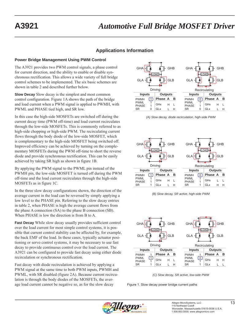
Power Bridge Management Using PWM Control
The A3921 provides two PWM control signals, a phase control for current direction, and the ability to enable or disable syn-chronous rectification. This allows a wide variety of full bridge control schemes to be implemented. The six basic schemes are shown in table 2 and described further below.
Slow Decay Slow decay is the simplest and most common control configuration. Figure 1A shows the path of the bridge and load current when a PWM signal is applied to PWMH, with PWML and PHASE tied high, and SR low.
In this case the high-side MOSFETs are switched off during the current decay time (PWM off-time) and load current recirculates through the low-side MOSFETs. This is commonly referred to as high-side chopping or high-side PWM. The recirculating current flows through the body diode of the low-side MOSFET, which is complementary to the high-side MOSFET being switched off. Improved efficiency can be achieved by turning on the comple-mentary MOSFETs during the PWM off-time to short the reverse diode and provide synchronous rectification. This can be easily achieved by taking SR high as shown in figure 1B.
By applying the PWM signal to the PWML pin instead of the PWMH pin, the low-side MOSFET is turned off during the PWM off-time and the load current recirculates through the high-side MOSFETs as in figure 1C.
In the three slow decay configurations shown, the direction of the average current in the load can be reversed by simply applying a low level to the PHASE pin. Referring to the slow decay entries in table 2, when PHASE is high the average current flows from the phase A connection (SA) to the phase B connection (SB). When PHASE is low the direction is from B to A.
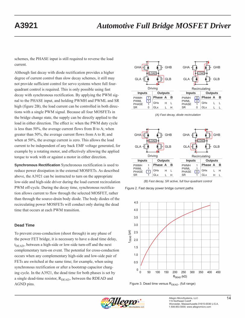
Fast Decay While slow decay usually provides sufficient control over the load current for most simple control systems, it is pos-sible that current control stability can be affected by, for example, the back EMF of the load. In these cases, typically actuator posi-tioning or servo control systems, it may be necessary to use fast decay to provide continuous control over the load current. The A3921 can be configured to provide fast decay using either diode recirculation or synchronous rectification.
Fast decay with diode recirculation is achieved by applying a PWM signal at the same time to both PWM inputs, PWMH and PWML, with SR disabled (figure 2A). Because current recircu-lation is through the body diodes of the MOSFETs, the aver-age load current cannot be negative so, as for the slow decay
Applications Information
Driving Recirculating
1110 L
HHL
PhasePWMHPWMLPHASESR
GHxGLx
Inputs
GHA
GLA
GHB
GLB
OutputsA B 0
110 L
HHL
PhasePWMHPWMLPHASESR
GHxGLx
Inputs
GHA
GLA
GHB
GLB
OutputsA B
Driving Recirculating
1111 L
HHL
PhasePWMHPWMLPHASESR
GHxGLx
Inputs
GHA
GLA
GHB
GLB
OutputsA B 0
111 H
LHL
PhasePWMHPWMLPHASESR
GHxGLx
Inputs
GHA
GLA
GHB
GLB
OutputsA B
Driving Recirculating
1111 L
HHL
PhasePWMHPWMLPHASESR
GHxGLx
Inputs
GHA
GLA
GHB
GLB
OutputsA B 1
011 L
HLH
PhasePWMHPWMLPHASESR
GHxGLx
Inputs
GHA
GLA
GHB
GLB
OutputsA B
LOAD LOAD
LOAD LOAD
LOAD LOAD
(A) Slow decay, diode recirculation, high-side PWM
(B) Slow decay, SR active, high-side PWM
(C) Slow decay, SR active, low-side PWM
Figure 1. Slow decay power bridge current paths
Automotive Full Bridge MOSFET DriverA3921
14Allegro MicroSystems, LLC115 Northeast CutoffWorcester, Massachusetts 01615-0036 U.S.A.1.508.853.5000; www.allegromicro.com
schemes, the PHASE input is still required to reverse the load current.
Although fast decay with diode rectification provides a higher degree of current control than slow decay schemes, it still may not provide sufficient control for servo systems where full four-quadrant control is required. This is only possible using fast decay with synchronous rectification. By applying the PWM sig-nal to the PHASE input, and holding PWMH and PWML and SR high (figure 2B), the load current can be controlled in both direc-tions with a single PWM signal. Because all four MOSFETs in the bridge change state, the supply can be directly applied to the load in either direction. The effect is: when the PWM duty cycle is less than 50%, the average current flows from B to A; when greater than 50%, the average current flows from A to B; and when at 50%, the average current is zero. This allows the load current to be independent of any back EMF voltage generated, for example by a rotating motor, and effectively allowing the applied torque to work with or against a motor in either direction.
Synchronous Rectification Synchronous rectification is used to reduce power dissipation in the external MOSFETs. As described above, the A3921 can be instructed to turn on the appropriate low-side and high-side driver during the load current recirculation PWM off-cycle. During the decay time, synchronous rectifica-tion allows current to flow through the selected MOSFET, rather than through the source-drain body diode. The body diodes of the recirculating power MOSFETs will conduct only during the dead time that occurs at each PWM transition.
Dead Time
To prevent cross-conduction (shoot through) in any phase of the power FET bridge, it is necessary to have a dead time delay, tDEAD , between a high-side or low-side turn-off and the next complementary turn-on event. The potential for cross-conduction occurs when any complementary high-side and low-side pair of FETs are switched at the same time; for example, when using synchronous rectification or after a bootstrap capacitor charg-ing cycle. In the A3921, the dead time for both phases is set by a single dead-time resistor, RDEAD , between the RDEAD and AGND pins.
Driving Recirculating
1110 L
HHL
PhasePWMHPWMLPHASESR
GHxGLx
Inputs
GHA
GLA
GHB
GLB
OutputsA B 0
010 L
LLL
PhasePWMHPWMLPHASESR
GHxGLx
Inputs
GHA
GLA
GHB
GLB
OutputsA B
Driving Recirculating
1111 L
HHL
PhasePWMHPWMLPHASESR
GHxGLx
Inputs
GHA
GLA
GHB
GLB
OutputsA B 1
101 H
LLH
PhasePWMHPWMLPHASESR
GHxGLx
Inputs
GHA
GLA
GHB
GLB
OutputsA B
LOAD LOAD
LOAD LOAD
(A) Fast decay, diode recirculation
(B) Fast decay, SR active, full four-quadrant control
Figure 2. Fast decay power bridge current paths
0.5
1.0
1.5
2.0
2.5
3.0
3.5
4.0
4.5
0 50 200100 150 250 300 350 400 450
t DEA
D (μ
s)
RDEAD (kΩ)
0
Figure 3. Dead time versus RDEAD , (full range)

Automotive Full Bridge MOSFET DriverA3921
15Allegro MicroSystems, LLC115 Northeast CutoffWorcester, Massachusetts 01615-0036 U.S.A.1.508.853.5000; www.allegromicro.com
For RDEAD values between 3 kΩ and 240 kΩ, at 25°C the nomi-nal value of tDEAD in ns can be approximated by:
72001.2 + (200 / RDEAD)
tDEAD(nom) ,50 +=
(1)
where RDEAD is in kΩ. Greatest accuracy is obtained for values of RDEAD between 6 and 60 kΩ, which are shown in figure 3.
The IDEAD current can be estimated by:
1.2RDEAD
IDEAD .=
(2)
The maximum dead time, 6 μs typical, can be set by connecting the RDEAD pin directly to the V5 pin.
The choice of power FET and external series gate resistance determine the selection of the dead-time resistor, RDEAD. The dead time should be long enough to ensure that one FET in a phase has stopped conducting before the complementary FET starts conducting. This should also take into account the tolerance and variation of the FET gate capacitance, the series gate resis-tance, and the on-resistance of the A3921 internal drives.
Dead time will be present only if the on-command for one FET occurs within tDEAD after the off-command for its complementary FET. In the case where one side of a phase drive is permanently off, for example when using diode rectification with slow decay, then the dead time will not occur. In this case the gate drive will turn on within the specified propagation delay after the corre-sponding phase input goes high. (Refer to the Gate Drive Timing diagrams.)
Fault Blank Time
To avoid false short fault detection, the output from the VDS monitor for any FET is ignored when that FET is off and for a period of time after it is turned on. This period of time is the fault blank time. Its length is the dead time, tDEAD , plus an additional period of time that compensates for the delay in the VDS moni-tors. This additional delay is typically 300 to 600 ns.
Braking
The A3921 can be used to perform dynamic braking either by forcing all low-side FETs on and all high-side FETs off (SR=1, PWMH=0, and PWML=1) or conversely by forcing all low-side FETs off and all high-side FETs on (SR=1, PWMH=1, and
PWML=0). This effectively short-circuits the back EMF of the motor, creating a breaking torque.
During braking, the load current can be approximated by:
VBEMF
RLIBRAKE ,=
(3)
where VBEMF is the voltage generated by the motor and RL is the resistance of the phase winding.
Care must be taken during braking to ensure that maximum rat-ings of the power FETs are not exceeded. Dynamic braking is equivalent to slow decay with synchronous rectification.
Bootstrap Capacitor Selection
The bootstrap capacitors, CBOOTx, must be correctly selected to ensure proper operation of the A3921. If the capacitances are too high, time will be wasted charging the capacitor, resulting in a limit on the maximum duty cycle and the PWM frequency. If the capacitances are too low, there can be a large voltage drop at the time the charge is transferred from CBOOTx to the FET gate, due to charge sharing.
To keep this voltage drop small, the charge in the bootstrap capacitor, QBOOT, should be much larger than the charge required by the gate of the FET, QGATE. A factor of 20 is a reasonable value, and the following formula can be used to calculate the value for CBOOT :
QBOOT CBOOT × VBOOT = QGATE × 20 , =
therefore:
QGATE × 20,
VBOOTCBOOT =
(4)
where VBOOT is the voltage across the bootstrap capacitor.
The voltage drop across the bootstrap capacitor as the FET is being turned on, ∆V , can be approximated by:
QGATE .CBOOT
∆V ≈
(5)
So, for a factor of 20, ∆V would be approximately 5% of VBOOT .
The maximum voltage across the bootstrap capacitor under normal operating conditions is VREG(max). However, in some circumstances the voltage may transiently reach 18 V, the clamp
Automotive Full Bridge MOSFET DriverA3921
16Allegro MicroSystems, LLC115 Northeast CutoffWorcester, Massachusetts 01615-0036 U.S.A.1.508.853.5000; www.allegromicro.com
voltage of the Zener diodes between the Cx and Sx pins. In most applications, with a good ceramic capacitor the working voltage can be limited to 16 V.
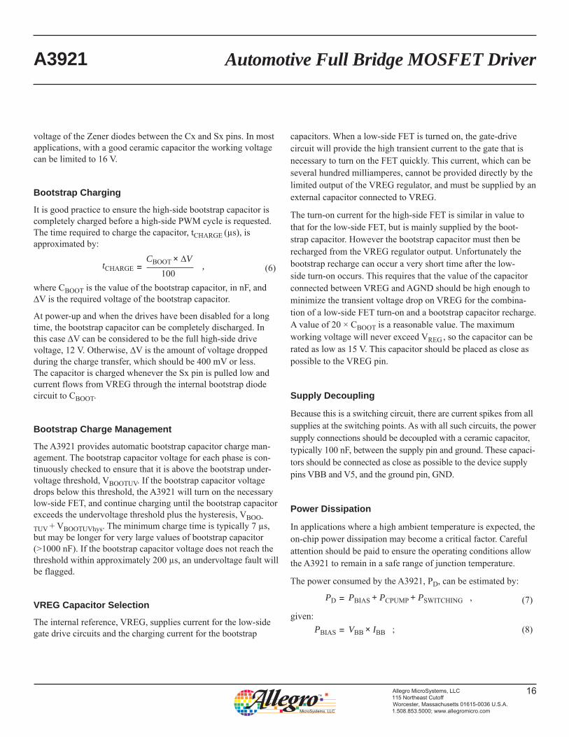
Bootstrap Charging
It is good practice to ensure the high-side bootstrap capacitor is completely charged before a high-side PWM cycle is requested. The time required to charge the capacitor, tCHARGE (μs), is approximated by:
CBOOT × ∆V,
100=tCHARGE
(6)
where CBOOT is the value of the bootstrap capacitor, in nF, and ∆V is the required voltage of the bootstrap capacitor.
At power-up and when the drives have been disabled for a long time, the bootstrap capacitor can be completely discharged. In this case ∆V can be considered to be the full high-side drive voltage, 12 V. Otherwise, ∆V is the amount of voltage dropped during the charge transfer, which should be 400 mV or less. The capacitor is charged whenever the Sx pin is pulled low and current flows from VREG through the internal bootstrap diode circuit to CBOOT.
Bootstrap Charge Management
The A3921 provides automatic bootstrap capacitor charge man-agement. The bootstrap capacitor voltage for each phase is con-tinuously checked to ensure that it is above the bootstrap under-voltage threshold, VBOOTUV. If the bootstrap capacitor voltage drops below this threshold, the A3921 will turn on the necessary low-side FET, and continue charging until the bootstrap capacitor exceeds the undervoltage threshold plus the hysteresis, VBOO-TUV + VBOOTUVhys. The minimum charge time is typically 7 μs, but may be longer for very large values of bootstrap capacitor (>1000 nF). If the bootstrap capacitor voltage does not reach the threshold within approximately 200 μs, an undervoltage fault will be flagged.
VREG Capacitor Selection
The internal reference, VREG, supplies current for the low-side gate drive circuits and the charging current for the bootstrap
capacitors. When a low-side FET is turned on, the gate-drive circuit will provide the high transient current to the gate that is necessary to turn on the FET quickly. This current, which can be several hundred milliamperes, cannot be provided directly by the limited output of the VREG regulator, and must be supplied by an external capacitor connected to VREG.
The turn-on current for the high-side FET is similar in value to that for the low-side FET, but is mainly supplied by the boot-strap capacitor. However the bootstrap capacitor must then be recharged from the VREG regulator output. Unfortunately the bootstrap recharge can occur a very short time after the low-side turn-on occurs. This requires that the value of the capacitor connected between VREG and AGND should be high enough to minimize the transient voltage drop on VREG for the combina-tion of a low-side FET turn-on and a bootstrap capacitor recharge. A value of 20 × CBOOT is a reasonable value. The maximum working voltage will never exceed VREG , so the capacitor can be rated as low as 15 V. This capacitor should be placed as close as possible to the VREG pin.
Supply Decoupling
Because this is a switching circuit, there are current spikes from all supplies at the switching points. As with all such circuits, the power supply connections should be decoupled with a ceramic capacitor, typically 100 nF, between the supply pin and ground. These capaci-tors should be connected as close as possible to the device supply pins VBB and V5, and the ground pin, GND.
Power Dissipation
In applications where a high ambient temperature is expected, the on-chip power dissipation may become a critical factor. Careful attention should be paid to ensure the operating conditions allow the A3921 to remain in a safe range of junction temperature.
The power consumed by the A3921, PD, can be estimated by:
PD PBIAS + PCPUMP + PSWITCHING ,= (7)
given:
PBIAS VBB × IBB ;= (8)
Automotive Full Bridge MOSFET DriverA3921
17Allegro MicroSystems, LLC115 Northeast CutoffWorcester, Massachusetts 01615-0036 U.S.A.1.508.853.5000; www.allegromicro.com
PCPUMPor
[( 2 VBB) – VREG] IAV , for VBB < 15 V, =
[VBB – VREG] IAV , for VBB ≥ 15 V, = (9)
PSWITCHING QGATE × VREG × N × fPWM × Ratio ; = (10)
where:IAV QGATE × N × fPWM , =
N is the number of FETs switching during a PWM cycle, and
Ratio
RGATE + 10.10=
N = 1 for slow decay with diode recirculation, N = 2 for slow decay with synchronous rectification or for fast decay with diode recir-culation, and N = 4 for fast decay with synchronous rectification.
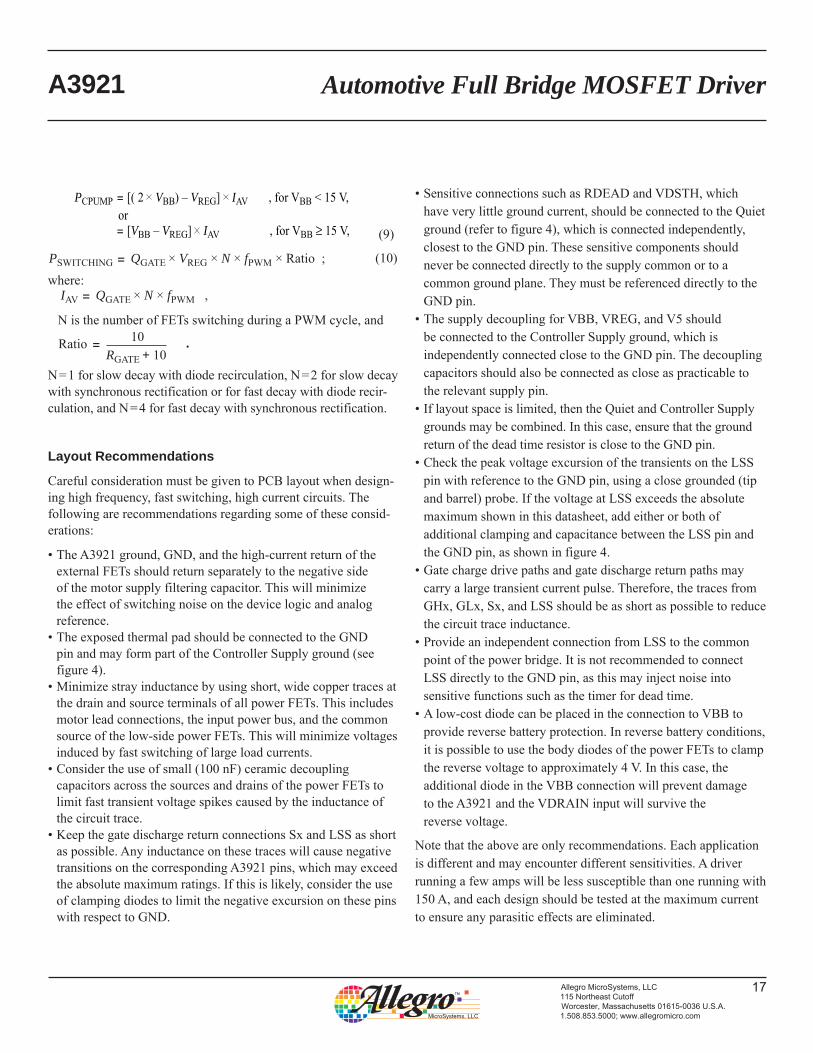
Layout Recommendations
Careful consideration must be given to PCB layout when design-ing high frequency, fast switching, high current circuits. The following are recommendations regarding some of these consid-erations:
• The A3921 ground, GND, and the high-current return of the external FETs should return separately to the negative side of the motor supply filtering capacitor. This will minimize the effect of switching noise on the device logic and analog reference.
• The exposed thermal pad should be connected to the GND pin and may form part of the Controller Supply ground (see figure 4).
• Minimize stray inductance by using short, wide copper traces at the drain and source terminals of all power FETs. This includes motor lead connections, the input power bus, and the common source of the low-side power FETs. This will minimize voltages induced by fast switching of large load currents.
• Consider the use of small (100 nF) ceramic decoupling capacitors across the sources and drains of the power FETs to limit fast transient voltage spikes caused by the inductance of the circuit trace.
• Keep the gate discharge return connections Sx and LSS as short as possible. Any inductance on these traces will cause negative transitions on the corresponding A3921 pins, which may exceed the absolute maximum ratings. If this is likely, consider the use of clamping diodes to limit the negative excursion on these pins with respect to GND.
• Sensitive connections such as RDEAD and VDSTH, which have very little ground current, should be connected to the Quiet ground (refer to figure 4), which is connected independently, closest to the GND pin. These sensitive components should never be connected directly to the supply common or to a common ground plane. They must be referenced directly to the GND pin.
• The supply decoupling for VBB, VREG, and V5 should be connected to the Controller Supply ground, which is independently connected close to the GND pin. The decoupling capacitors should also be connected as close as practicable to the relevant supply pin.
• If layout space is limited, then the Quiet and Controller Supply grounds may be combined. In this case, ensure that the ground return of the dead time resistor is close to the GND pin.
• Check the peak voltage excursion of the transients on the LSS pin with reference to the GND pin, using a close grounded (tip and barrel) probe. If the voltage at LSS exceeds the absolute maximum shown in this datasheet, add either or both of additional clamping and capacitance between the LSS pin and the GND pin, as shown in figure 4.
• Gate charge drive paths and gate discharge return paths may carry a large transient current pulse. Therefore, the traces from GHx, GLx, Sx, and LSS should be as short as possible to reduce the circuit trace inductance.
• Provide an independent connection from LSS to the common point of the power bridge. It is not recommended to connect LSS directly to the GND pin, as this may inject noise into sensitive functions such as the timer for dead time.
• A low-cost diode can be placed in the connection to VBB to provide reverse battery protection. In reverse battery conditions, it is possible to use the body diodes of the power FETs to clamp the reverse voltage to approximately 4 V. In this case, the additional diode in the VBB connection will prevent damage to the A3921 and the VDRAIN input will survive the reverse voltage.
Note that the above are only recommendations. Each application is different and may encounter different sensitivities. A driver running a few amps will be less susceptible than one running with 150 A, and each design should be tested at the maximum current to ensure any parasitic effects are eliminated.
Automotive Full Bridge MOSFET DriverA3921
18Allegro MicroSystems, LLC115 Northeast CutoffWorcester, Massachusetts 01615-0036 U.S.A.1.508.853.5000; www.allegromicro.com
Figure 4. Supply routing suggestions
SA
GHA
GLA
LSS
Supply Common
+ Supply
Motor
VBB
VREG
VS
VDSTH
RDEAD
Quiet Ground
Controller Supply Ground
Power Ground
A3921
GHB
GLB
SB
VDRAIN
Optional components to limit LSS transients
RSGND
Optional reverse battery protection
VDRAIN
19 V
19 V
20 V
VBB
VBB
18 V
18 V
18 V
VS
6 V
CP1
18 V
CP2
1 kΩ
8.5 V
PWMxSR
PHASE
3 kΩ
ESD
RESET3 kΩ
6 V 6 V
50 kΩ
8.5 V
VDSTH
ESD
RDEAD100 Ω
8.5 V
1.2 V
ESDESD
FFx
ESD
10 Ω
Cx
18 VGHx
Sx
GLx
LSS
20 V
18 V18 V
VREG
Input and Output Structures
(A) Gate drive outputs
(B) Supply protection structures
(C) Fault output (D) RESET input
(E) Logic inputs, no pulldown (G) RDEAD(F) VDS monitor threshold input
Automotive Full Bridge MOSFET DriverA3921
19Allegro MicroSystems, LLC115 Northeast CutoffWorcester, Massachusetts 01615-0036 U.S.A.1.508.853.5000; www.allegromicro.com
VDRAIN
LSS
GLB
SB
GHB
CB
NC
VREG
CA
GHA
SA
GLA
VBB
NC
VDSTH
RDEAD
FF2
FF1
RESET
PWMH
PWML
SR
V5
PHASE
NC
GND
CP1
CP2
28
27
26
25
24
23
22
21
20
19
18
17
16
15
1
2
3
4
5
6
7
8
9
10
11
12
13
14
Con
trol L
ogic
Reg
Charge Pump
tDEAD
Reg
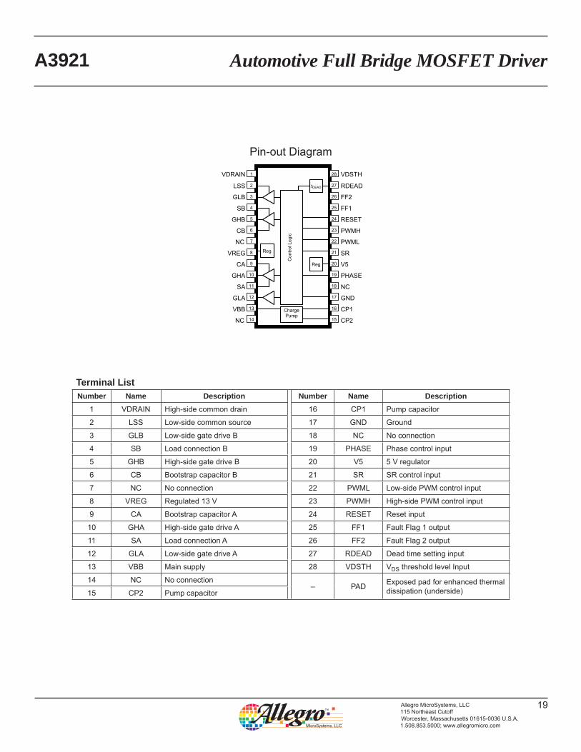
Pin-out Diagram
Terminal ListNumber Name Description Number Name Description
1 VDRAIN High-side common drain 16 CP1 Pump capacitor
2 LSS Low-side common source 17 GND Ground
3 GLB Low-side gate drive B 18 NC No connection
4 SB Load connection B 19 PHASE Phase control input
5 GHB High-side gate drive B 20 V5 5 V regulator
6 CB Bootstrap capacitor B 21 SR SR control input
7 NC No connection 22 PWML Low-side PWM control input
8 VREG Regulated 13 V 23 PWMH High-side PWM control input
9 CA Bootstrap capacitor A 24 RESET Reset input
10 GHA High-side gate drive A 25 FF1 Fault Flag 1 output
11 SA Load connection A 26 FF2 Fault Flag 2 output
12 GLA Low-side gate drive A 27 RDEAD Dead time setting input
13 VBB Main supply 28 VDSTH VDS threshold level Input
14 NC No connection– PAD Exposed pad for enhanced thermal
dissipation (underside)15 CP2 Pump capacitor

Automotive Full Bridge MOSFET DriverA3921
20Allegro MicroSystems, LLC115 Northeast CutoffWorcester, Massachusetts 01615-0036 U.S.A.1.508.853.5000; www.allegromicro.com
Package LP 28-Pin TSSOP with Exposed Thermal Pad
1.20 MAX
0.10 MAX
CSEATINGPLANEC0.10
28X
6.10
0.650.45
1.65
3.003.00
5.00
5.00
0.25
0.65
21
28
GAUGE PLANESEATING PLANE
B
A
28
21
A Terminal #1 mark area
B
For reference only(reference JEDEC MO-153 AET)Dimensions in millimetersDimensions exclusive of mold flash, gate burrs, and dambar protrusions Exact case and lead configuration at supplier discretion within limits shown
Reference land pattern layout (reference IPC7351 SOP65P640X120-29CM); All pads a minimum of 0.20 mm from all adjacent pads; adjust as necessary to meet application process requirements and PCB layout tolerances; when mounting on a multilayer PCB, thermal vias at the exposed thermal pad land can improve thermal dissipation (reference EIA/JEDEC Standard JESD51-5)
PCB Layout Reference View
Exposed thermal pad (bottom surface)
4.40 ±0.10 6.40 ±0.20
(1.00)
9.70 ±0.10
C
C
0.60 ±0.15
4° ±4
0.15 +0.05–0.06
0.25 +0.05–0.06

Automotive Full Bridge MOSFET DriverA3921
21Allegro MicroSystems, LLC115 Northeast CutoffWorcester, Massachusetts 01615-0036 U.S.A.1.508.853.5000; www.allegromicro.com
Copyright ©2011-2013, Allegro MicroSystems, LLCAllegro MicroSystems, LLC reserves the right to make, from time to time, such de par tures from the detail spec i fi ca tions as may be required to
permit improvements in the per for mance, reliability, or manufacturability of its products. Before placing an order, the user is cautioned to verify that the information being relied upon is current.
Allegro’s products are not to be used in life support devices or systems, if a failure of an Allegro product can reasonably be expected to cause the failure of that life support device or system, or to affect the safety or effectiveness of that device or system.
The in for ma tion in clud ed herein is believed to be ac cu rate and reliable. How ev er, Allegro MicroSystems, LLC assumes no re spon si bil i ty for its use; nor for any in fringe ment of patents or other rights of third parties which may result from its use.
For the latest version of this document, visit our website:www.allegromicro.com